Embed Size (px)
Citation preview
Comparative study on the properties of ZnO
nanowires and nanocrystalline thin films
Esteban Broitman, C Bojorge, F Elhordoy, V. Kent, G Zanini Gadioli, R. Marotti,
H Canepa and E. A. Dalchiele
Linköping University Post Print
N.B.: When citing this work, cite the original article.
Original Publication:
Esteban Broitman, C Bojorge, F Elhordoy, V. Kent, G Zanini Gadioli, R. Marotti, H Canepa
and E. A. Dalchiele, Comparative study on the properties of ZnO nanowires and
nanocrystalline thin films, 2012, Surface & Coatings Technology, (213), 59-64.
http://dx.doi.org/10.1016/j.surfcoat.2012.10.015
Copyright: Elsevier
http://www.elsevier.com/
Postprint available at: Linköping University Electronic Press
http://urn.kb.se/resolve?urn=urn:nbn:se:liu:diva-88519
1
Comparative Study on the Properties of ZnO Nanowires and Nanocrystalline Thin Films
E. Broitman1,*, C. Bojorge2, F. Elhordoy3, V. R. Kent3,
G. Zanini Gadioli4, R. E. Marotti3, H. Cánepa2, E. A. Dalchiele3
1Thin Film Physics Division, IFM, Linköping University, SE 581-83 Linköping, Sweden.
2 CINSO, CITEDEF-CONICET, B1603ALO Villa Martelli, Argentina.
3 Instituto de Física & CINQUIFIMA, Facultad de Ingeniería, UdelaR, CP 11000 Montevideo,
Uruguay.
4 Instituto de Física Gleb Wataghin, UNICAMP, 13083-970 Campinas, SP, Brazil.
(*) Corresponding autor: [email protected] ; Fax:+46-13-137568
Keywords
ZnO; ZnO nanowires; nanocrystaline ZnO; sol gel; water adsorption

2
Abstract
The microstructural, morphological, optical and water-adsorption properties
of nanocrystalline ZnO thin films and ZnO nanowires were studied and compared.
The ZnO thin films were obtained by a sol-gel process, while the ZnO nanowires
were electrochemically grown onto a ZnO sol-gel spin-coated seed layer. Thin films
and nanowires samples were deposited onto crystalline quartz substrates covered
by an Au electrode, able to be used in a quartz crystal microbalance. X-ray
diffraction measurements reveal in both cases a typical diffraction pattern of ZnO
wurtzite structure. Scanning electron microscopic images of nanowires samples
show the presence of nanowires with hexagonal sections, with diameters ranging
from 30 to 90 nm. Optical characterization reveals a bandgap energy of 3.29 eV for
the nanowires and 3.35 eV for the thin films. A quartz crystal microbalance placed
in a vacuum chamber was used to quantify the amount and kinetics of water
adsorption onto the samples. Nanowire samples, which have higher surface areas
than the thin films, adsorb significantly more water.
3
1. Introduction
Nanostructures made of wurtzite ZnO, such as nanowires (NWs) and
nanocrystals, are receiving increasing attention because of potential applications in
optoelectronic devices, gas sensing elements, detectors, highly efficient photonic
devices, near-UV lasers, photovoltaic solar cells, etc. [1, 2, 3]. Ü. Özgür et al and
D.C. Look have comprehensively reviewed the properties and applications of ZnO
as both, thin film (TF) and nanostructured materials [4, 5]. Both publications have
stressed the synthesis and application of nanostructured ZnO, such as NWs,
nanorods, and nanobelts, because their morphologies and properties can be
modified and controlled through synthesis. Size reduction in nanostructured ZnO
materials lead to quantum confinement effects, which in turn impart novel
electrical, mechanical, chemical, and optical properties to ZnO [6, 7, 8]. Another
example is the application in photovoltaic solar cells, where the morphology of NW
arrays has been observed to improve both the light collection and charge
extraction [9, 10].
Schmidt-Mende et al. have described a two-step synthesis of ZnO NWs: in
the first step the substrate is coated with a seed layer of ZnO nanoparticles; in the
second step, NWs are grown on top of the seed layer, which provides nucleation
centers [2]. Different deposition methods can be used for each step resulting in
nanostructures that have different properties. Chemical vapor deposition and
thermal evaporation have been the most commonly used routes for the synthesis
of nanocrystaline films, NWs, nanobelts, nanosprings and nanorings, which have
been well summarized by Wang [11]. More recently, electrodeposition, sol-gel and

4
other aqueous solution growth techniques have also attracted great interest
because they are relatively economical methods that allow growth of
nanostructures at low temperatures and over large areas [2, 7, 12].
Recently we have developed a novel approach to growth of ZnO NWs by a
two-step method that combines different techniques [13]. In the first step a seed
layer of ZnO nucleation centers is prepared by a sol–gel method; in the second
step, NWs are grown on the seed layer by electrochemical deposition. To our
knowledge, this was the first time that these two techniques have been combined
for ZnO NW preparation [13]. The present study compares the morphology,
microstructure, and optical properties of nanostructured ZnO TFs and ZnO NWs
grown by this novel technique. Also, the water adsorption at ZnO TF and NW
surfaces is measured to compare their surface reactivity.
2. Experimental
2.1 Sample preparation
ZnO TFs and ZnO NWs were grown onto single-crystal quartz substrates of
about 1.5 cm2 area covered by a circular Au electrode, for use in a quartz crystal
microbalance (QCM).
Films were prepared by sol-gel process from a precursor solution of zinc
acetate dehydrate in ethyl alcohol, with deionized water and acetic acid added for
the hydrolysis reaction [6, 14]. The sol was stirred at 65º C for 1 h with reflux to
become clear and homogeneous. After aging for 24 hr at room temperature, ZnO
TFs were deposited by spin coating (3000 rpm, 15 s) the sol onto the substrate and
5
then drying at 150º C for 10 min; four spin coats were applied to obtain thicker
films. Samples received a thermal treatment at 370 ºC during 3 h to transform the
deposited ZnO layers into a nanocrystalline film. Samples were prepared
depositing the ZnO TFs on one or both sides of the quartz crystal.
ZnO NWs were electrochemically grown onto the ZnO seed layer deposited
on the Au circular electrode side of the quartz crystal. Before growth, acrylic paint
was used to mask the back of the quartz crystal and the periphery of the front side
of the crystal, leaving an effective NWs coated area of about 0.5 cm2. The ZnO
seed layer was deposited by the same spin coating technique used for the TFs
with final heat treatment at 370º C for 1h. ZnO NWs were electrochemically grown
onto this seed layer. Electrodeposition was performed in a conventional three-
electrode electrochemical cell with the substrate as the cathode, a Zn sheet as the
counter electrode, and a saturated calomel electrode (SCE) as the reference
electrode. The electrolyte was an aqueous solution of the Zn+2 precursor (1 mM
zinc acetate) and a supporting electrolyte (0.1 M sodium acetate), saturated with
bubbling oxygen. The ultra pure water (18 MΩ-cm) was provided by a Millipore
equipment. ZnO NW arrays were electrodeposited at 70º C under potentiostatic
conditions at – 1.000 V vs. SCE for 70 min. The initial pH was adjusted to 6.76.
The final sample was washed with deionized water to remove any residual salt
[13].

6
2.2 Sample Characterization
Structural characterization of the ZnO TFs and ZnO NW arrays was
performed by X-ray diffraction (XRD) using a Philips PW3710 diffractometer with
CuKα radiation operating with glancing angle geometry (GIXRD) at a constant
incidence angle αi =1º. Scanning electron microscopy (SEM) images were obtained
with a LEO SEM equipment operated at 5 kV.
The optical properties of the samples were studied by diffuse reflectance
spectroscopy rather than transmittance spectroscopy due to the optically opaque
Au back contact [15]. A 1000 W electric power Xe lamp (ORIEL 6271) light source
was used for this measurement. The light was chopped with an SRS SR540
chopper and monochromated with an ORIEL 77250 monochromator. The reflected
light (normal detection and quasi-normal incidence [16]) was detected by a UV
enhanced unbiased silicon detector of 100 mm2 area (UDT 11-09-001-1). A first
lock-in amplifier (SRS SR530) extracted the signal from the detector, while a
second lock-in amplifier (EG&G 5209) was used to measure the variation of the
optical source amplitude, correcting its variations in the first lock-in through the
ratio output. A PC controlled the entire process (monochromator movement and
GPIB communication with the lock-in). Measurements were performed at room
temperature.
7
2.3 Water adsorption measurement on ZnO TFs and NWs
The apparatus designed and constructed for measurement of water vapor
adsorption onto ZnO films has been described previously [17, 18]. It consists of a
vacuum chamber that can be evacuated by either a turbopump or a sorption pump
and operates in the pressure range of 10−6–104 Torr. The turbopump was used to
achieve an initial base pressure of 10−6 Torr; the sorption pump was used during
the experiments to avoid vibrations affecting the microbalance. A capacitance
manometer was used to measure the partial pressure of water in the range 10-4–
104 Torr. The QCM housing is capable of holding 3 quartz crystals for
simultaneously monitoring of water adsorption on three surfaces. The temperature
of the QCM is measured by a K-type thermocouple spot-welded to the quartz
crystal housing. The equivalence between %RH and water partial pressure at a
given temperature was calculated from the empirical correlation that can be used
to estimate the saturated vapor pressure as a function of temperature [19]. A time-
resolved QCM-D from Q-Sense with a resolution of 0.01 Hz was used to measure
the change in the resonance frequency via a USB interface connected to a
computer.
The QCM was used to measure the mass of water adsorbed onto the ZnO
TFs and NWs deposited over the gold-coated quartz crystal surface. QCM is a
mass sensitive device based on the measurement of the change in resonant
frequency of a gold-coated quartz crystal. When water is adsorbed onto these
surface, the mass change (Δm) can be calculated from the frequency change (Δf)
of the crystal resonance by using the Sauerbrey equation:
8
22 of
fAm
(1)
where fo is the resonant frequency of the fundamental mode of the crystal, A is the
area of the gold disk coated onto the crystal (1.53936 cm2), is the density of the
crystal (2.684 g/cm3), and µ is the shear modulus of quartz (2.947 x 10¹¹ g/cm s2)
[20]. Around the resonance frequency of 6 MHz, a net change of 100 Hz
corresponds to approximated 6 ng of water adsorbed or desorbed onto the surface
of the crystal.
The QCM resonance frequency depends also on the crystal temperature; for
our crystals, a change of 0.1 oC corresponds to a frequency change of
approximately 0.1 Hz [21]. To avoid artifacts from temperature changes during the
experiments, the crystal holder and the chamber were held at a fixed temperature
of 50.0 ± 0.1 oC using a temperature-controlled water circulation system [20].
3. Results and Discussion
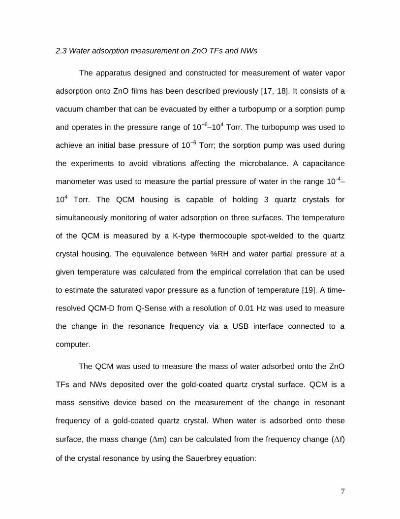
3.1 Morphology
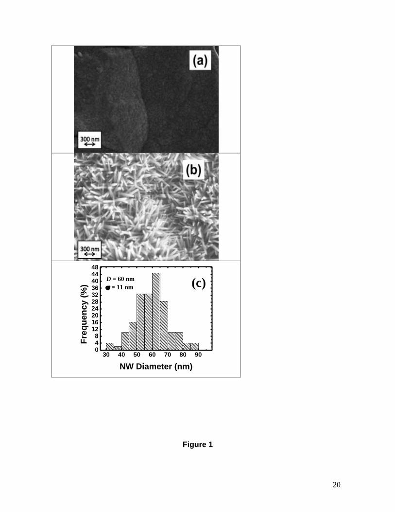
The SEM image of figure 1a shows the morphology of a ZnO TF grown onto
a single-crystal gold-coated quartz substrate. The surface is relatively smooth, and
follows the gold polycrystalline substrate surface. Figure 1b shows the
corresponding morphology of NWs electrodeposited at an electrochemical potential
of – 1000 mV. The size range of the NWs’ diameters is 30 to 90 nm, as indicated in
9
Fig. 1c. The mean size is about 60 nm, with a dispersion of 11 nm, while the most
probable value is between 60 and 65 nm. A closer inspection reveals that the NWs
have hexagonal section [13], consistent with their wurtzite structure (see section
3.2). The ZnO NWs grow following the morphology already present in the seed TF
layer. This leads to an overall net increase of the sample surface. If we consider
that a typical NW has a mean diameter of 62.5 nm and mean length of 500 nm,
and that there are 6.88 x 10⁹ nanowires/cm2 (measured on SEM images), the
masked surface of 0.5 cm2 will have a real surface of about 3.4 cm2, which
corresponds to a surface increase of approximately 7:1.
3.2 Chemical composition and microstructure
Energy-dispersive X-ray spectroscopy analysis (not shown here) has
indicated the presence of only two elements, oxygen and Zn, in both TFs and NWs
samples.
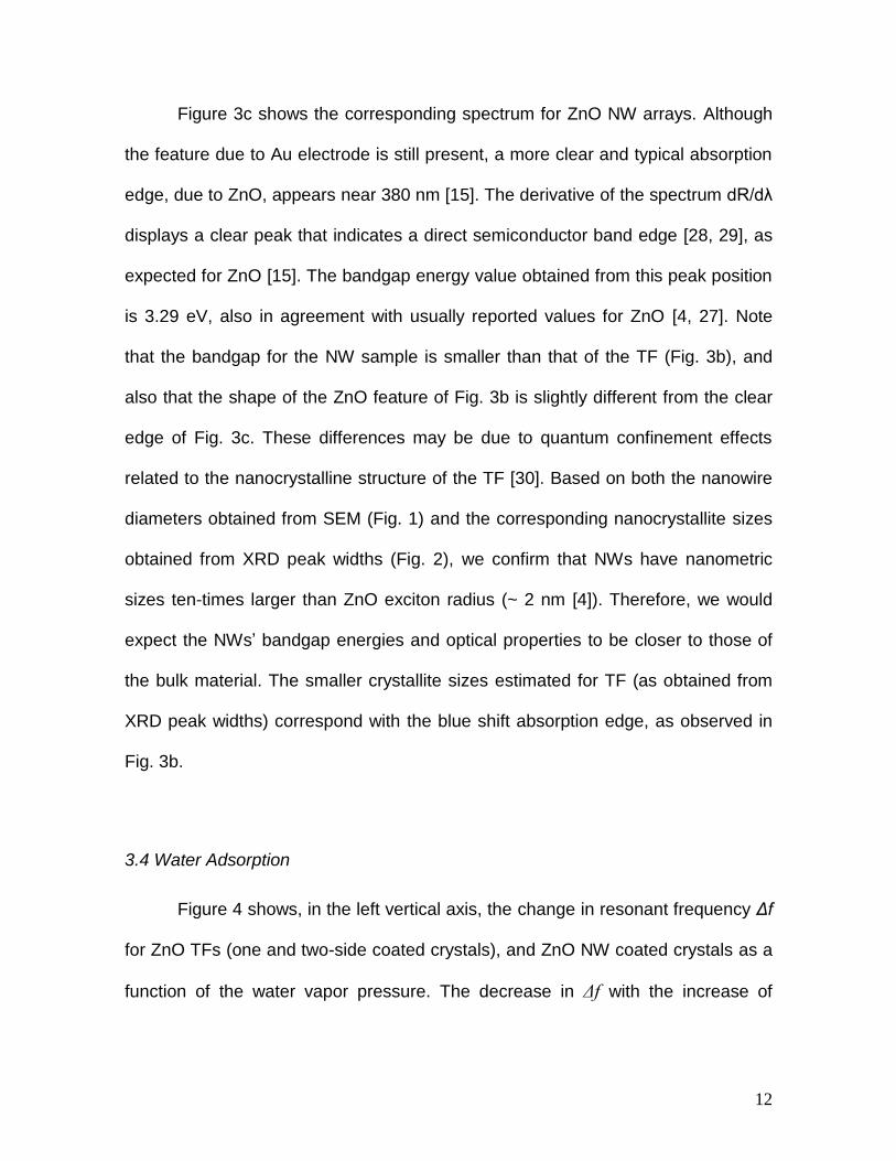
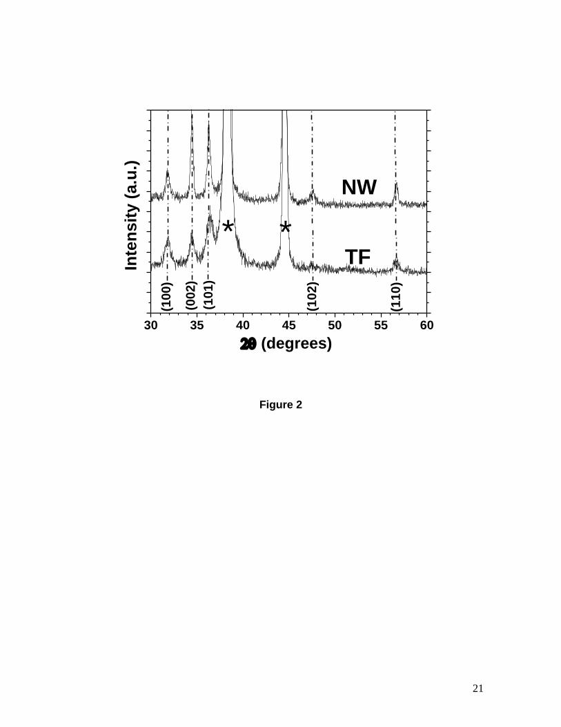
Figure 2 shows XRD results for the ZnO samples. The diffraction peaks
labeled with an asterisk correspond to the Au layer on the substrate. The X-ray
diffraction patterns of TFs and NWs are similar, with diffraction peaks
corresponding to the wurtzite (hexagonal) structure of ZnO (space group P63mc)
reported for a standard bulk ZnO in the Joint Committee of Powder Diffraction
Standards (JCPDS) card file data [22]. No diffraction features characteristics of
other phases were detected in the patterns, suggesting that only single-phase ZnO
samples were deposited. The TFs diffraction features are wider than the NWs
features, probably due to higher surface stresses and/or smaller crystallite size in
10
the films. Assuming only size broadening (uniform strain within each crystallite), an
estimation of crystallite size D can be obtained using Scherrer's equation [23]:
)cos(
kD
(2)
where the constant k is the shape factor close to 1, λ the wavelength of the X-ray, θ
the Bragg's angle and β is the full width at half maxima. The XRD peak can be
widened by internal stress and defects, so the mean grain size estimated by this
method is normally smaller than the actual value [24].
For the TF samples, the corresponding widths for the (100), (002) and (101)
diffraction peaks are 0.637o, 0.552o and 1.065o, respectively. If an instrumental
width on the order of 0.3o is taken into account, the grain sizes are in the range of
10 to 33 nm.
For the NWs samples, the corresponding widths for the (100), (002) and
(101) diffraction peaks are 0.419o, 0.252o and 0.434o, respectively. The size along
the [002] direction is above the range obtainable by this determination, while the
widths along the other directions are in the range of 65 to 75 nm, in agreement with
the sizes observed by SEM in figure 1b and 1c.
The nanowire exhibits the strongest orientation of the c-axis perpendicular to
the surface of the substrate, represented by the (002) reflection, suggesting that
the nanowires grow along the [002] direction, as we previously reported [13]. The
other observed orientations, originated in the beginning of the deposition, are
impeded to continue growing whereas it is favored the growth of NWs aligned
11
perpendicularly to the substrate [25]. Furthermore, the (002) diffraction peak has a
relative higher intensity for the NWs than for the TFs (Fig. 2), suggesting a higher
texture coefficient along the (002) diffraction peak [26]. The quantification of the
texture is, however, difficult because of the vertical shift of the (101) diffraction due
to its proximity to a large Au feature
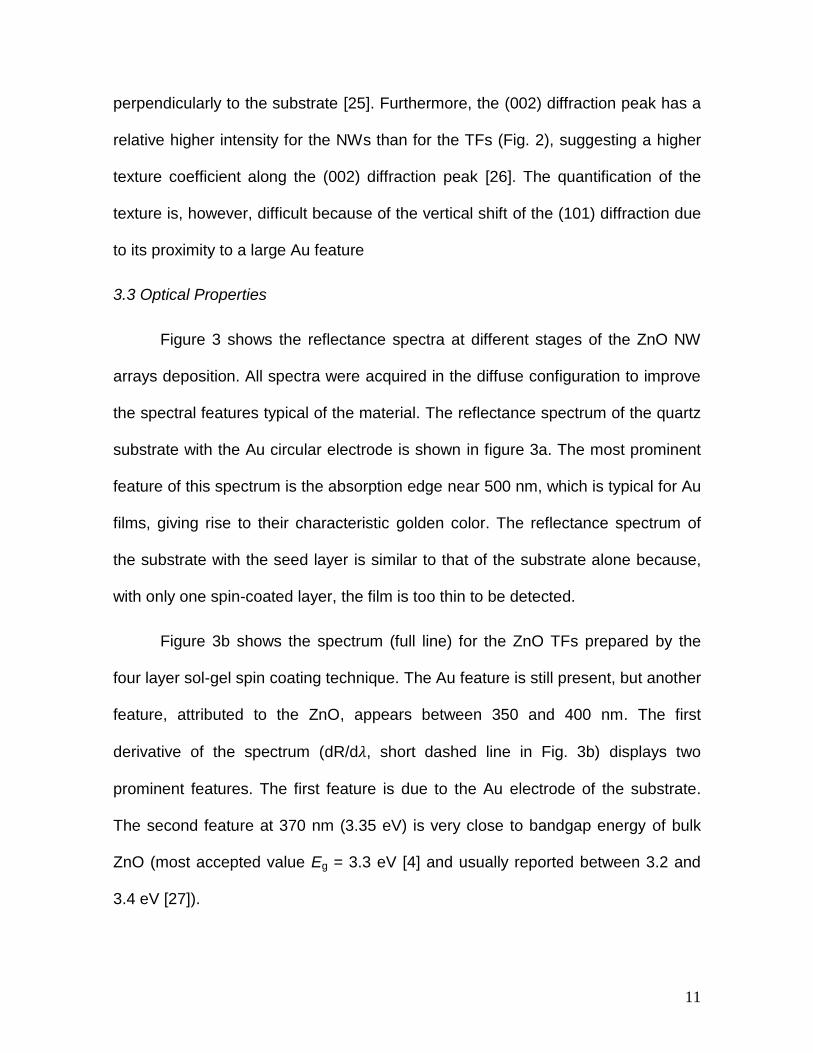
3.3 Optical Properties
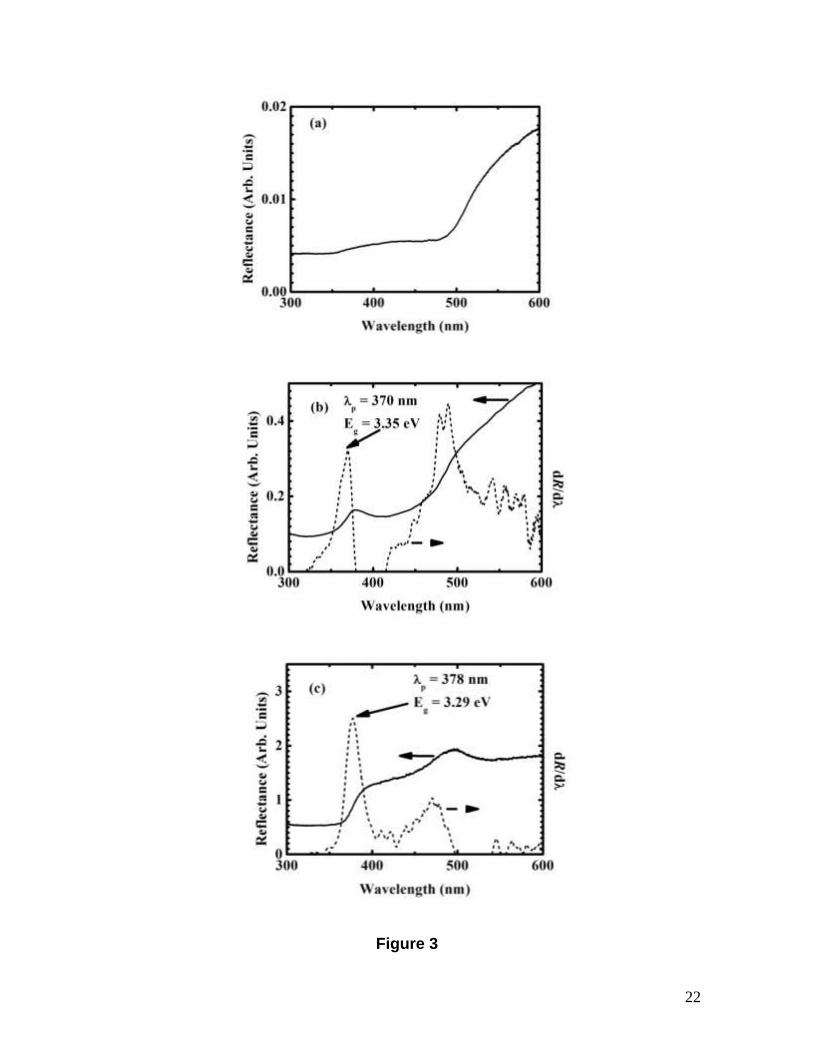
Figure 3 shows the reflectance spectra at different stages of the ZnO NW
arrays deposition. All spectra were acquired in the diffuse configuration to improve
the spectral features typical of the material. The reflectance spectrum of the quartz
substrate with the Au circular electrode is shown in figure 3a. The most prominent
feature of this spectrum is the absorption edge near 500 nm, which is typical for Au
films, giving rise to their characteristic golden color. The reflectance spectrum of
the substrate with the seed layer is similar to that of the substrate alone because,
with only one spin-coated layer, the film is too thin to be detected.
Figure 3b shows the spectrum (full line) for the ZnO TFs prepared by the
four layer sol-gel spin coating technique. The Au feature is still present, but another
feature, attributed to the ZnO, appears between 350 and 400 nm. The first
derivative of the spectrum (dR/d𝜆, short dashed line in Fig. 3b) displays two
prominent features. The first feature is due to the Au electrode of the substrate.
The second feature at 370 nm (3.35 eV) is very close to bandgap energy of bulk
ZnO (most accepted value Eg = 3.3 eV [4] and usually reported between 3.2 and
3.4 eV [27]).
12
Figure 3c shows the corresponding spectrum for ZnO NW arrays. Although
the feature due to Au electrode is still present, a more clear and typical absorption
edge, due to ZnO, appears near 380 nm [15]. The derivative of the spectrum dR/dλ
displays a clear peak that indicates a direct semiconductor band edge [28, 29], as
expected for ZnO [15]. The bandgap energy value obtained from this peak position
is 3.29 eV, also in agreement with usually reported values for ZnO [4, 27]. Note
that the bandgap for the NW sample is smaller than that of the TF (Fig. 3b), and
also that the shape of the ZnO feature of Fig. 3b is slightly different from the clear
edge of Fig. 3c. These differences may be due to quantum confinement effects
related to the nanocrystalline structure of the TF [30]. Based on both the nanowire
diameters obtained from SEM (Fig. 1) and the corresponding nanocrystallite sizes
obtained from XRD peak widths (Fig. 2), we confirm that NWs have nanometric
sizes ten-times larger than ZnO exciton radius (~ 2 nm [4]). Therefore, we would
expect the NWs’ bandgap energies and optical properties to be closer to those of
the bulk material. The smaller crystallite sizes estimated for TF (as obtained from
XRD peak widths) correspond with the blue shift absorption edge, as observed in
Fig. 3b.
3.4 Water Adsorption
Figure 4 shows, in the left vertical axis, the change in resonant frequency Δf
for ZnO TFs (one and two-side coated crystals), and ZnO NW coated crystals as a
function of the water vapor pressure. The decrease in Δf with the increase of
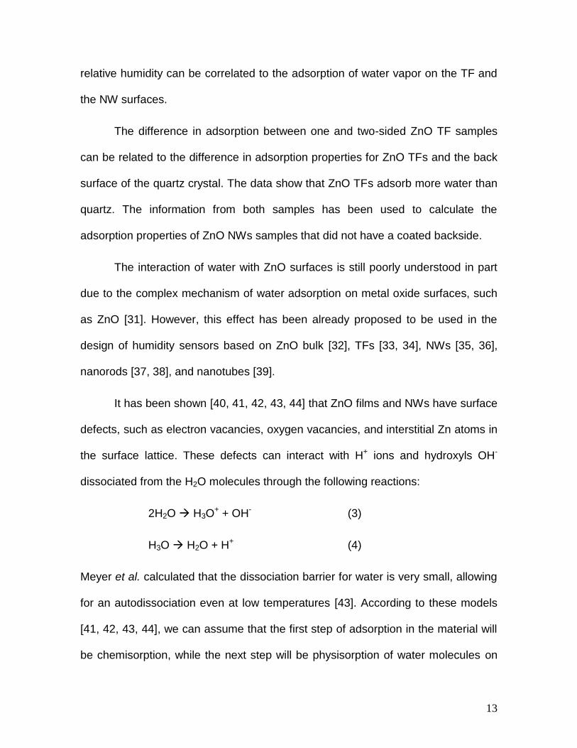
13
relative humidity can be correlated to the adsorption of water vapor on the TF and
the NW surfaces.
The difference in adsorption between one and two-sided ZnO TF samples
can be related to the difference in adsorption properties for ZnO TFs and the back
surface of the quartz crystal. The data show that ZnO TFs adsorb more water than
quartz. The information from both samples has been used to calculate the
adsorption properties of ZnO NWs samples that did not have a coated backside.
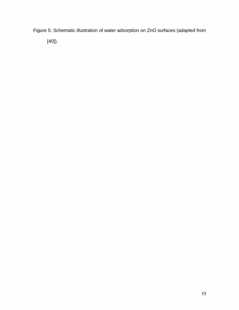
The interaction of water with ZnO surfaces is still poorly understood in part
due to the complex mechanism of water adsorption on metal oxide surfaces, such
as ZnO [31]. However, this effect has been already proposed to be used in the
design of humidity sensors based on ZnO bulk [32], TFs [33, 34], NWs [35, 36],
nanorods [37, 38], and nanotubes [39].
It has been shown [40, 41, 42, 43, 44] that ZnO films and NWs have surface
defects, such as electron vacancies, oxygen vacancies, and interstitial Zn atoms in
the surface lattice. These defects can interact with H+ ions and hydroxyls OH-
dissociated from the H2O molecules through the following reactions:
2H2O H3O+ + OH- (3)
H3O H2O + H+ (4)
Meyer et al. calculated that the dissociation barrier for water is very small, allowing
for an autodissociation even at low temperatures [43]. According to these models
[41, 42, 43, 44], we can assume that the first step of adsorption in the material will
be chemisorption, while the next step will be physisorption of water molecules on
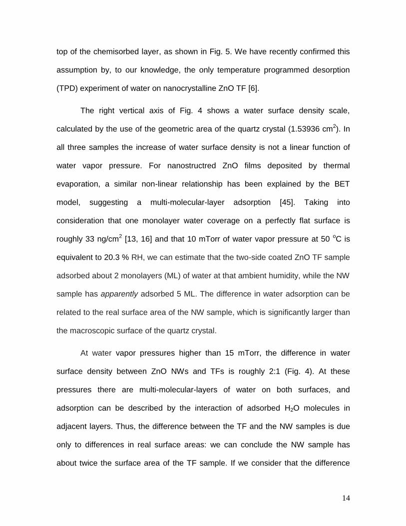
14
top of the chemisorbed layer, as shown in Fig. 5. We have recently confirmed this
assumption by, to our knowledge, the only temperature programmed desorption
(TPD) experiment of water on nanocrystalline ZnO TF [6].
The right vertical axis of Fig. 4 shows a water surface density scale,
calculated by the use of the geometric area of the quartz crystal (1.53936 cm2). In
all three samples the increase of water surface density is not a linear function of
water vapor pressure. For nanostructred ZnO films deposited by thermal
evaporation, a similar non-linear relationship has been explained by the BET
model, suggesting a multi-molecular-layer adsorption [45]. Taking into
consideration that one monolayer water coverage on a perfectly flat surface is
roughly 33 ng/cm2 [13, 16] and that 10 mTorr of water vapor pressure at 50 oC is
equivalent to 20.3 % RH, we can estimate that the two-side coated ZnO TF sample
adsorbed about 2 monolayers (ML) of water at that ambient humidity, while the NW
sample has apparently adsorbed 5 ML. The difference in water adsorption can be
related to the real surface area of the NW sample, which is significantly larger than
the macroscopic surface of the quartz crystal.
At water vapor pressures higher than 15 mTorr, the difference in water
surface density between ZnO NWs and TFs is roughly 2:1 (Fig. 4). At these
pressures there are multi-molecular-layers of water on both surfaces, and
adsorption can be described by the interaction of adsorbed H2O molecules in
adjacent layers. Thus, the difference between the TF and the NW samples is due
only to differences in real surface areas: we can conclude the NW sample has
about twice the surface area of the TF sample. If we consider that the difference

15
between the TFs and NWs samples originates in a ~0.5 cm2 region containing
nanowires, we can estimate from the results at high pressure in Fig. 4 that the
small surface has increased roughly seven times its area. This value agrees well
with the estimate from SEM characterization that was described in section 3.1.
At water vapor pressures lower than 15 mTorr, NWs have a higher
sensitivity than the TFs. Erol et al., analyzing QCM results by using a modified
Langmuir adsorption isotherm model, have shown that a higher adsorption rate can
be correlated to a larger number of available adsorption sites [38]. It has also been
shown that ZnO NWs, represented as hexagonal prisms, have a high number of
defects on their faceted side-walls [44]. The presence of more active sites to
interact with humidity molecules on the walls of the NWs increases their surface
reactivity and sensitivity compared to the flat TF samples. As a result, more
adsorbed humidity molecules at these active sites cause an increase in the
adsorption rate at low water vapor pressures.
3. Conclusions
Nanocrystalline ZnO thin films and ZnO nanowires were studied and
compared. Both the ZnO thin films obtained by a sol-gel process and the
electrochemically grown ZnO nanowires have the same wurtzite structure.
Neglecting the influence of strain in XRD peak widths, nanocrystallites with sizes
between 10 and 33 nm were obtained for ZnO thin films while elongated shapes
with 60 nm mean diameter were obtained for ZnO nanowires grown onto a ZnO
sol-gel spin-coated seed layer. SEM morphological studies revealed nanowires
16
with hexagonal sections, consistent with their hexagonal wurtzite structure, and
diameters between 30 and 90 nm.
The optical properties of the nanowire array confirm the presence of a direct
semiconductor absorption edge, with bandgap energy at 3.29 eV, close to
accepted value for ZnO. The optical properties of ZnO thin films (with bandgap
energy at 3.35 eV) are influenced by quantum size effects due to the small
dimensions of their primary nanocrystalline structure, while the optical properties of
ZnO nanowires are not affected due to their relative larger nanometric diameter.
QCM measurements quantified the amount of adsorbed water and
adsorption kinetics for ZnO thin films and nanowires. Occupying the same
macroscopic area, one-dimensional nanowires adsorbed larger amounts of water
because they have a higher surface-to-volume ratio than thin films. ZnO nanowires
are more sensitive to low water vapor pressures (i.e., low %RH) than ZnO thin
films, likely due to a higher number of defects on their walls.
4. Acknowledgements
This work was partially supported by CNPq (Brazil, Prosul Program,
Project # 490580/2008-4) and CLAF. The authors gratefully acknowledge helpful
discussions with Prof. J.B. Miller from Carnegie Mellon University. E.B
acknowledges the support from the Swedish Government Strategic Research Area
Grant in Materials Science, and Prof. A.J. Gellman from Carnegie Mellon
University for the use of his QCM adsorption chamber. C.B. thanks to M.E.F de
Rapp and J. Casanova for their help in XRD experiments and to CITEDEF and
17
CONICET for financial support. F.E., V.R.K., E.A.D. and R.E.M. acknowledge the
support received from PEDECIBA–Física, ANII (Agencia Nacional de Investigación
e Innovación) and the CSIC (Comisión Sectorial de Investigación Científica) from
the Universidad de la República, in Montevideo, Uruguay.
18
Figure Captions:
Figure 1: (a) SEM image of a ZnO thin film deposited onto a single-crystal gold-
coated quartz substrate (b) SEM image of a ZnO NW array electrodeposited
at – 1000 mV. (c) Corresponding size dispersion, where D is the mean
nanowire diameter and its standard deviation.
Figure 2: XRD for TFs (lower curve) and NWs (upper curve). Peaks labeled with “*”
are originated from the Au substrate. The vertical dotted lines correspond to
the published JCPDS pattern [22].
Figure 3: Optical properties of (a) substrate (Au electrode deposited onto quartz
substrate), (b) ZnO TF deposited onto substrate by four-layer spin coating,
and (c) ZnO NW arrays electrodeposited at – 1000 mV. In (b) and (c), the
full lines are the reflectance spectra while short dotted lines are the first
derivative against wavelength.
Figure 4: Water adsorption versus water pressure for (a) one side ZnO TF coated
substrate; (b) two-sides ZnO TF coated substrate; (c) one-side ZnO NW
coated substrate. The left vertical axis shows the decrease in resonant
frequency f of the quartz crystal, and the right vertical axis shows a water
surface density scale, calculated by the use of the geometrical area of the
quartz crystal. The dashed line indicates one monolayer of water coverage
on a perfect flat surface (33 ng/cm2)
19
Figure 5: Schematic illustration of water adsorption on ZnO surfaces (adapted from
[40]).
20
30 40 50 60 70 80 90048
12162024283236404448
Fre
qu
en
cy
(%
)
NW Diameter (nm)
(c)D = 60 nm
= 11 nm
Figure 1
(b)
21
30 35 40 45 50 55 60
TF*
(11
0)
(10
2)
(101)
(002)
(100)
In
ten
sit
y (
a.u
.)
(degrees)
*
NW
Figure 2
22
Figure 3

23
0 5 10 15 20 25
0
50
100
150
200
250
f
(Hz)
TF-1
TF-2
NW
Water Vapor Pressure (mTorr)
Wa
ter
Su
rfa
ce
De
ns
ity
(n
g/c
m2)-13.15
-10.52
-7.89
-5.26
-2.63
0.00
Figure 4

24
Figure 5
O
O O
H H
H
O
H H
O
H H
H H
O
H H
Chemisorbed hydroxils
O O O O
H H H H H H H H
First physisorbed layer
Second physisorbed layer
25
5. Bibliography
[1] Z. Fan and J. G. Lu, "Zinc Oxide Nanostructures: Synthesis and Properties," Journal
of Nanoscience and Nanotechnology, vol. 5, pp. 1561-1573, 2005.
[2] L. Schmidt-Mende and J. L. MacManus-Driscoll, "ZnO - nanostructures, defects, and
devices," Materials Today, vol. 10, pp. 40-48, 2007.
[3] D. P. Norton, Y. W. Heo, M. P. Ivill, K. Ip, S. J. Pearton, M. F. Chisholm and T.
Steiner, "ZnO: Growth, doping & processing," Materials Today, vol. 7, pp. 34-40,
2004.
[4] Ü. Özgür, Y. I. Alivov and Y. I. Liu, "A comprehensive review of ZnO materials and
devices," Applied Physics Reviews, vol. 98, p. 041301, 2001.
[5] D. C. Look, "Recent advances in ZnO materials and devices," Materials Science and
Engineering B, vol. 80, pp. 383-387, 2001.
[6] R. E. Marotti, C. D. Bojorge, E. Broitman, H. R. Canepa, J. A. Badan, E. A. Dalchiele
and A. J. Gellman, "Characterization of ZnO and ZnO:Al Thin Films Deposited by the
Sol-Gel Dip-Coating Technique," Thin Solid Films, vol. 517, pp. 1077-1080, 2008.
[7] C. N. R. Rao, F. L. Deepak, G. Gundiah and A. Govindaraj, "Inorganic nanowires,"
Progress in Solid State Chemistry, vol. 31, pp. 5-147, 2003.
[8] B. Sonawane, M. Bhole and D. Patil, "Effect of magnesium incorporation in zinc oxide
films for optical waveguide applications," Physica B: Condensed Matte, vol. 405, no.
6, pp. 1603-1607, 2010.
[9] B. M. Kayes, H. A. Atwater and N. S. Lewis, "Comparison of the device physics
principles of planar and radial p-n junction nanorod solar cells," J. Appl. Phys., vol. 97,
pp. 114302-1-114302-11, 2005.
[10] Tena-Zaera, J. Jamil Elias and C. Lévy-Clément, "ZnO nanowire arrays: Optical
scattering and sensitization to solar light," Appl. Phys. Lett., vol. 97, pp. 233119-1-
233119-3, 2008.
[11] Z. L. Wang, "Piezoelectric Nanostructures: From Growth Phenomena to Electric
Nanogenerators," MRS Bulletin, vol. 32, p. 109, 2007.
[12] V. Shelke, M. Bhole and D. Patil, "Open air annealing effect on the electrical and
optical properties of tin doped ZnO nanostructure," Solid State Sciences, vol. 14, no. 6,
pp. 705-710, 2012.
[13] C. D. Bojorge, V. R. Kent, E. Teliz, H. R. Canepa, R. Henrıquez, H. Gomez, R. E.
Marotti and E. A. Dalchiele, "Zinc-oxide nanowires electrochemically grown onto sol–
gel spin-coated seed layers," Phys. Status Solidi A, vol. 208, p. 1662–1669, 2011.
[14] L. Armelao, M. Fabrizio, S. Gialanella and F. Zordan, "Sol–gel synthesis and
characterisation of ZnO-based nanosystems," Thin Solid Films, vol. 394, pp. 89-95,
2001.
26
[15] R. E. Marotti, D. N. Guerra, C. Bello, G. Machado and E. A. Dalchiele, "Bandgap
Energy Tuning of Electrochemically Grown ZnO Thin Films by Thickness and
Electrodeposition Potential," Solar Energy Materials and Solar Cells, vol. 82, pp. 85-
103, 2004.
[16] S. R. Johnson and T. Tiedje, "Temperature dependence of the Urbach edge in GaAs,"
J. Appl. Phys., vol. 87, p. 5609, 1995.
[17] E. Broitman, G. K. Gueorguiev, A. Furlan, N. T. Son, A. J. Gellman, S. Stafström and
L. Hultman, "Water adsorption on fullerene-like carbon nitride overcoats," Thin Solid
Films, vol. 517, pp. 1106-1110, 2008.
[18] E. Broitman, A. Furlan, G. K. Gueorguiev, Z. Czigany, A. M. Tarditi, A. J. Gellman,
S. Stafstrom and L. Hultman, "Water adsorption on phosphorous-carbide thin films,"
Surface and Coatings Technology, vol. 204, pp. 1035-1039, 2009.
[19] A. L. Buck, "New Equations for Computing Vapor Pressure and Enhancement,"
Journal of Applied Metereology, vol. 20, pp. 1527-1532, 1981.
[20] E. Broitman, V. V. Pushkarev, A. J. Gellman, J. Neidhardt, A. Furlan and L. Hultman,
"Water adsorption on lubricated fullerene-like CNx films," Thin Solid Films, vol. 515,
pp. 979-985, 2006.
[21] M. N. Rocklein and S. M. George, "Temperature-Induced Apparent Mass Changes
Observed during Quartz Crystal Microbalance Measurements of Atomic Layer
Deposition," Anal. Chem., vol. 75, pp. 4975-4982, 2003.
[22] JCPDS File 5-0664: ZnO, Joint Committee of Powder Diffraction Standards, 1999.
[23] B. Cullity, Elements of X-ray Diffraction, 2nd ed., Reading, MA: Addison Wesley,
1978.
[24] D. Raoufi and T. Raoufi, "The effect of heat treatment on the physical properties of
sol–gel derived ZnO thin films," Applied Surface Science, vol. 255, no. 11, pp. 5812-
5817, 2009.
[25] O. Lupan, V. Guérin, I. Tiginyanu, V. Ursaki, L. Chow, H. Heinrich and T. Pauporté,
"Well-aligned arrays of vertically oriented ZnO nanowires electrodeposited on ITO-
coated glass and their integration in dye sensitized solar cells," Journal of
Photochemistry and Photobiology A: Chemistry, vol. 211, pp. 65-73, 2010.
[26] D. Ariosa, F. Elhordoy, E. Dalchiele, R. E. Marotti and C. Stari, "Texture vs
morphology in ZnO nano-rods: on the XRD characterization of electrochemically
grown samples," J. Appl. Phys., vol. 110, p. 124901, 2011.
[27] R. Bhargava, "Wide Bandgap II-VI Semiconductors," in EMIS Datareviews Series No
17, London, INSPEC, 1997, p. 27 and 179.
[28] G. Riveros, H. Gómez, R. Henríquez, R. Schrebler, R. E. Marotti and E. A. Dalchiele,
"Electrodeposition and Characterization of ZnSe Semiconductor Thin Films," Solar
Energy Materials and Solar Cells, vol. 70, pp. 255-268, 2001.
[29] G. Riveros, H. Gómez, R. Henríquez, R. Schrebler, R. E. Marotti and E. A. Dalchiele,
"Electrodoposition and Characterization of ZnX (X=Se, Te) Semiconductor Thin
Films," Boletín de la Sociedad Chilena de Química, vol. 47, pp. 411-429, 2002.
[30] C. D. Bojorge, H. R. Cánepa, U. E. Gilabert, D. Silva, E. A. Dalchiele and R. E.
Marotti, "Synthesis and optical characterization of ZnO and ZnO:Al nanocrystalline
27
films obtained by the sol-gel dip-coating process," Journal of Material Science:
Materials in Electronics, vol. 18, pp. 1119-1122, 2007.
[31] Y. Li, F. D. Valle, M. Simonnet, I. Yamada and J.-J. Delaunay, "Competitive surface
effects of oxygen and water on UV photoresponse of ZnO nanowires," Appl. Phys.
Lett., vol. 94, p. 023110, 2009.
[32] N. K. Pandey and K. Tiwari, "Morphological and Relative Humidity Sensing
Properties of Pure ZnO Nanomaterial," Sensors & Transducers Journal, vol. 122, pp.
9-19, 2010.
[33] S. Dixit, A. Srivastava and R. K. Shukla, "Effect of toxic gases on humidity sensing
property of nanocrystalline ZnO film," J. Appl. Phys., vol. 102, p. 113114, 2007.
[34] V. Musat, A. M. Rego, R. Monteiro and E. Fortunato, "Microstructure and gas sensing
properties of sol-gel ZnO thin films," Thin Solid Films, vol. 516, pp. 1512-1515, 2008.
[35] S.-P. Chang, S.-J. Chang, C.-Y. Lu, M.-J. Li, C.-L. Hsu, Y.-Z. Chiou, T.-J. Hsuej and
I.-C. Chen, "ZnO film as humidity sensor," Superlatices and Microstructures, vol. 47,
pp. 772-778, 2010.
[36] X. Qiu, J. Oiler, J. Zhu, Z. Wang, R. Tang, C. Yu and H. Yu, "Film Bulk Acoustic-
Wave Resonator Based Relative Humidity Sensor Using ZnO Films," Electrochem.
Solid-State Lett., vol. 13, pp. J65-J67, 2010.
[37] F. Fang, J. Futter, A. Markwitz and J. Kennedy, "UV and humidity sensing properties
of ZnO nanorods prepared by the arc discharge method," Nanotechnology, vol. 20, p.
245502, 2009.
[38] Y. Wang, J. T. W. Yeow and L.-Y. Chen, "Synthesis of Aligned ZnO nanorods with
different Parameters and Their Effects on Humidity Sensing," in Recent Advances in
Sensing Technology, G. S. Gupta and Y. R. Huang, Eds., Berlin, Springer-Verlag,
2009, pp. 257-269.
[39] J. Han, F. Fan, C. Xu, S. Lin, M. Wei, X. Duan and Z. L. Wang, "ZnO nanotube-based
dye-sensitized solar cell and its application in self-powered devices," Nanotechnology,
vol. 21, p. 405203, 2010.
[40] B. C. Yadav, R. Srivastava and C. D. Dwivedi, "Synthesis and characterization of
ZnO-TiO2 nanocomposite and its application as a humidity sensor," Philosophical
Magazine, vol. 88, pp. 1113-1124, 2008.
[41] D. Raymand, A. C. T. v. Duin, D. Spångberg, W. A. Goddard and K. Hermansson,
"Water adsorption on stepped ZnO surfaces from MD simulation," Surface Science,
vol. 604, pp. 741-752, 2010.
[42] B. Meyer and D. Marx, "Density-functional study of the structure and stability of ZnO
surfaces," Physical Review B, vol. 67, p. 035403, 2003.
[43] B. Meyer, H. Rabaa and D. Marx, "Water adsorption on ZnO(10-10): From single
molecules to partially dissociated monolayers," Phys. Chem. Chem. Phys., vol. 8, pp.
1513-1521, 2006.
[44] Y. Dai, Y. Zhang, Y. Q. Bai and Z. L. Wang, "Bicrystalline zinc oxide nanowires,"
Chemical Physics Letters, vol. 375, pp. 96-101, 2003.
[45] X. Zhou, J. Zhang, T. Jiang, X. Wang and Z. Zhu, "Humidity detection by
nanostructured ZnO: a wireless quartz crystal microbalance investigation," Sensors

28
and Actuators A, vol. 135, pp. 209-214, 2007.