Embed Size (px)
Citation preview

\I\IABCC ~
An American-Standard Company
SERVICE MANUAL 6042 A
AVI ROUTE BUFFER PANEL
May, 1981 A-81-150-2286-3
(OPTION #1)
UNION SWITCH & SIGNAL DIVISION WESTINGHOUSE AIR BRAKE COMPANY
Swissvale, PA 15218

Wl;IBCCl ~
CONTENTS
I. GENERAL
1.1 PURPOSE 1.2 GENERAL DESCRIPTION 1.3 INDICATIONS
II. OPERATION
2.1 THEORY OF OPERATION 2.2. OUTPUT RATINGS
III. INSTALLATION
3.1 MOUNTING 3·. 2 INTERCONNECTIONS
IV. TROUBLESHOOTING
4.1 REQUIRED EQUIPMENT 4.2 INITIAL PROCEDURE 4.3 COMPLETE OPERATION CHECK 4.4 TROUBLESHOOTING PROCEDURE
4.4.1 Data Strobe and First Message Detector
4.4.2 Route Indications 4.4.3 Route Decoder and Relay Outputs 4.4.4 Test Mode and Power Up Reset
V. DRAWINGS AND PARTS LIST
ii
Page
1
1 1
. -, •
1 ....
3
3 3
5
5 5
5
5 5 6 7
7 8 9
10
12

JI
1.1 PURPOSE
SECTION I GENERAL
The purpose of the AVI Route Buffer Panel, when used in conjunction with the basic AVI Decoder Logic Unit, is to provide a means to locally decode the two digit route number into one of twenty possible route numbers. The two digit route number is obtained from the AVI message sent by the lead vehicle in a train. The decoded output is a contact closure of one of twenty relays, corresponding to route numbers 1 through 20, and is available to interface with external equipment to set up routes and/or indicate the destination of the train. Information is stored by the route buffer until the track circuit associated with the AVI equipment is cleared.
1.2 GENERAL DESCRIPTION
The TWC Route Buffer Panel is constructed on a 60-way wire wrap panel and is housed as part of the Decoder Logic Unit N451465-0301. The Route Buffer Panel accepts the parallel route data signals decoded by the Decoder Logic Panel N451412-0202 from the first message and energizes one of twenty route relays corresponding to routes 1 through 20. When the "Trak", "Lead Car 11
, and "Good Message" (GM) input signals are present from the Decoder Logic Panel, the route buffer will energize the corresponding relay as indicated by the route input data bits DB3 - DB8. Data input bits DB3 and DB4 give the tens digit of the route while data input bits DBS through DB8 indicate the units digit of the route. The route buffer accepts data only from the first message received when the LEAD Car bit (DB25) is present in that message. Seven LED's provide visual indication of the first message reception and the decoded route number in BCD (1, 2, 4, 8, 10 and 20). Route information is stored in the route buffer, from the time that the first message is received and decoded, until the track circuit is unoccupied. The heels of all of the route relays are bussed to a common "MN" (main neutral) relay. The route buffer output is disabled whenever the decoder is operated in either of the two test modes by disabling the main neutral relay, opening the "MN" common to the route relay contacts.
1.3 INDICATIONS
The label on the inside of the cover of the Decoder Logic Unit type N451565-0301 (Figure 1) shows the location of seven (7) LED's. Four of the LED's provide a visual indication of the
6042-A, p. 1

m ~~ 0 ~
~ I J6 I I J7 1 I Ja I I ~ ~ I I I I [ I " I I D t'(l
~ 11 Jb JT "' I •.. ~"1' I POWER SUPPLY
"" I I • I J4 =:..... UJ725836
POWER DIST. & INTERFACE ! ! ... v~ l.11 rm 111 I AC AC - + UN451055 -7301
Jl-10[ ··~]
r .... JJ2-9 J2-11 ' I I I
UNITS· 8 LIO FIRST MESSAGE 4 o TENS 2 0 o 20 I O O 10
BG20
ROUTE BUFFER UN451412-0201
I ~]JI-I
J2-4C ··~1 I I J2-2 I I
N ,·~ . !
IL.a I BGI
ERROR GOOD MESSAGE (;Jo MESSAGE
CARRIER DETECTOR O O TRACK
CAB O O KEY ON SIGNAL BG3
DECODER UN451412-0202
UN451465-0301
I TEST DECODJR I 2 NORMAL I I 3 TEST RECEIVER
TWISTED PAIR
~ TWISTED PAIR
If I I I I RECEIVER
UN451404-5501 I
Figure 1. Decoder Logic Unit Major Component Location
.._ ,.

WABCO ~·'V"
UNITS digit of the decoded route number in BCD form (1, 2, 4 and 8) and two others provide the TENS digit (10 and 20). The seventh LED provides an indication that the FIRST MESSAGE is received.
SECTION II
OPERATION
2.1 THEORY OF OPERATION
Figure 2 is a block diagram and Figures 3 and 4 are circuit diagrams of the Route Buffer Panel. Data bits DB3 through DBS are input on pins 3 through 8 of connector BJ2 on the Route Buffer Panel. These data bits are buffered by IC-A24 and stored in buffer ICs B25 and B30, four-bit parallel-in, parallel-out registers. The TRAK, LEAD CAR, and GOOD MESSAGE AND ERROR MESSAGE signals on pins 15, 25, and 16 of connector BJ2 are gated by IC-B24 and provide a trailing edge clock to First Message flip-flop IC-B29. Single shot IC-Bl8, along with IC-B23, provide a delay pulse circuit for the GOOD MESSAGE AND ERROR MESSAGE input signal. A reset First Message flip-flop IC-B29, the presence of LEAD CAR, and the delayed GOOD AND ERROR MESSAGE signal clocks the data into the storage buffers B25 and B30, which drive BCD to decimal decoders, Al8 and A23, thorugh appropriate gating and inversion by IC's A21, A26, A22 and Al7. The First Message flip-flop is set after the delayed GOOD AND ERROR MESSAGE pulse terminates, preventing data from being accepted from succeeding messages. IC's Bl9 and A17 provide drive to the FIRST MESSAGE LED and the route LED's 10, 20, 1, 2, 4 and 8. The route LED's 1, 2, 4 and 8 indicate the unit's digit of the route in BCD form, while the 10 and 20 LED's indicate the ten's digit of the route selected. The outputs of BCD decoder IC's (Al8 and A23) drive transistor arrays ICs All, Al2, Bl5 which provide the drive current for relays Kl through K20. The TEST signal on pin 17 of connector BJ2 drives the "MN" common relay K21 and inhibits data output in the test mode. All logic inputs to the route buffer are provided with a 100 Kohm pull-down resistor for input protection.
2.2 OUTPUT RATING
Note well: The relay contacts output from the Route Buffer are capable of handling 1/2 ampere, max. at 50 volts DC max., or 10 watts maximum DC resistive load.
6042-A, p. 3

°' 0 .;,,. N I
:i:, .. 'U
.;,,. LEAD CAR
GM+ EM
TRAK
MSTR
PARALLEL ROUTE INFORMATION DATA FROM DECODER
-., MESSAGE STROBE
LOGIC -.. ....
,, .. •• - DATA : :'.' STORAGE ~ REGISTERS : .
·- '
--. 1st 1st MESSAGE - MESSAGE . DETECTOR INDICATION ,... (LED)
•• •
BCD RELAY - TO DECIMAL ~ DRIVERS . RELAYS -. - .
DECODER --••
ROUTE INDICATION
(LEDS)
Figure 2. Route Buffer Panel Block Diagram
...,
.... ""JI' --. --. :'.' ~ .....
RELAY CONTACTS OUTPU'I'S
~I

SECTION III
INSTALLATION
3.1 MOUNTING
The Route Buffer Panel, N451412-0201 is mounted in the left front section of the Decoder Logic Unit, type N451465-0301, (Refer to Figure 1 for location). Mounting is accomplished by slipping the panel onto five #4x40 screws and securing with five lock washers and nuts.
3.2 INTERCONNECTIONS
WABCO '-/'"~
Electrical connections to the Decoder Logic Unit circuitry are made thr9ugh two ribbon cables with connectors. A cabling diagram is attached to the cover of the Decoder Logic Unit and is also shown in Figure 1. The cable from the Decoder Logic Panel is connected to BJ2 on the Route Buffer Panel and the cable from the Power Distribution and Interface PCB is connected to AJl on the Route Buffer Panel. Insure that the connectors are properly aligned before firmly mating the connectors to prevent possible damage due to misalignment.
SECTION IV
TROUBLESHOOTING
This procedure is intended as a guide for troubleshooting the Route Buffer Panel, N451412-0201, in the Decoder Logic Unit N451465-0301.
4.1 REQUIRED EQUIPMENT
Refer to AVI Service Manual 6042, Section 5.4.1 and 5.4.2 for required AVI equipment and suggested test equipment.
4.2 INITIAL PROCEDURE
1. Remove the ASCII or Route Buffer Panel, if any, from the Decoder Logic Unit of a complete working AVI system. (See AVI Service Manual 6042, Figures 5-12, 5-13 and 5-14 for complete system connections.)
2. Install the defective Route Buffer into the Decoder Logic Unit. (Wiring instructions are attached to the cover of a Decoder Logic Unit with Route Buffer N451465-0301.) See Figure 1.
6042-A, p. 5

WABCCI ~
3. Activate the Lead Car indication on the Programmer of the AVI system by applying 36 VDC to pin A of connector PS and common to pin B.
4. Remove the Transponder Coil from over the Wayside coil as pictured in Figure 5-13 in Service Manual 6042.
5. Place the Receiver PCB Test switch in the Decoder Logic Unit to the Normal position and switch on power. All indication LED's should be off.
6. Turn on the 12 VDC Track Indication power supply of Figure 5-14 (SM6042} connected between pins 11 and 13 of connector J7. The Key-On and Track LEDs of the Decoder Logic Unit should be lit, with a working Decoder, unless the TRAK signal is shorted on the Route Buffer Panel.
4.3 COMPLETE OPERATION CHECK
NOTE
If no problems are encountered during the succeeding steps, the Route Buffer is operational, otherwise see Troubleshooting Procedure, paragraph 4.4.
1. Check the First Message indication of the Route Buffer:
A. Pass the Transponder Coil (connected to a Programmer} over the Wayside Coil and remove. The FIRST MESSAGE LED on the Route Buffer should be lit.
B. Reset the Route Buffer by turning off the Track Indication power supply. All of the LEDs in the Decoder Logic Unit must turn off. Switch the Track Indication power supply back on; all of the LEDs on the Route Buffer should remain off.
2. If the FIRST MESSAGE LED is operating, check the relay contact outputs of the Route Buffer with an ohmmeter between "MN" common and the appropriate route outputs at connector AJl and observe the route indication LEDS for routes 0-20, set by the thumbwheel switches on the Programmer. Repeat parts 'A' and 'B' of Step 1 for each route, and compare the results to columns 2 and 3 of Table 1. Verify that no more than one of the route relays K01-K20 remain closed at any one time (Refer to Figure 4 for pin numbers on connector AJl.
6042-A, p. 6

WABCO 'v."4./
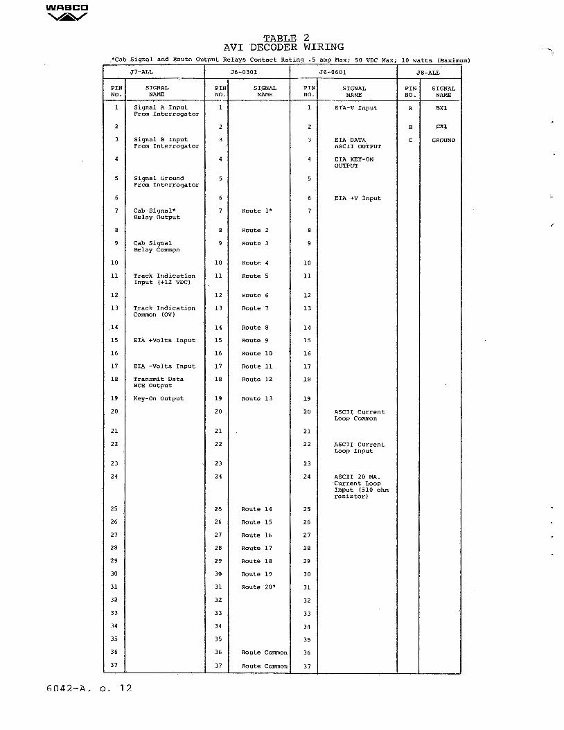
3. Repeat steps 1 and 2, checking the relay contact outputs on connector J6. (See Table 2 for connections.)
4. With an arbitrary route stored in the route buffer, place the Test switch on the Receiver PCB of the · Decoder Logic Unit to the Test Decoder position. The MN signal relay (K21) contacts should be open. Verify the open circuit between "MN' common and the route output on connector AJl. Return the Test switch to the Normal position.
5. With an arbitrary route selected on the Programmer, pass the Transponder Coil over the Wayside Coil and remove. Verify that the First Message LED and the correct route indication LEDs, as checked previously, are lit. Select a different route number on the Programmer and pass the Transponder Coil over the Wayside Coil again. The route indicator LEDs should not change and the FIRST MESSAGE LED should remain lit.
6. Switch off AC power to the Decoder Unit until all of the LEDs go out, then turn the Decoder Logic Unit back on. All of the LEDs on the Route Buffer should remain off.
4.4 TROUBLESHOOTING PROCEDURE
NOTE
To reset the Route Buffer for a First Message indication, turn off the Track Indication power supply until the LEDs in the Decoder Logic Unit go out; then turn back on.
4.4.1 Data Strobe and First Message Detector
The following procedure should be performed if any of the following problems exist:
A. No First Message indication is given. B. No route indications are given for any route. c. Second message causes. a change in the route indication.
1. With a dual channel oscilloscope or an equivalent logic analyzer, check the timing of the first 7 signals indicated on the Route Buffer Timing Diagram, Figure 5. Trigger the oscilloscope on the Good and Error Message signal at IC B24, pin 1.
2. Pass the Transponder Coil (which is connected to a Programmer) over the Wayside Coil and remove. The oscilloscope should trigger with a known good working
6042-A, p. 7

basic Decoder Panel unless the signals are shorted or open at the Route Buffer Panel.
3. Observe if the Trak, Lead Car, and Good Msg + Error Msg signals from the Decoder Panel are as indicated on the timing chart. If incorrect signals are received, check the cable connector between the Decoder and Route Buffer Panels for shorted or open wires; also, check ICs B23, Bl8, B24 and connections on the Route Buffer Panel.
4. The signals at the single shots (B18), the First Message flip-flop {B29-15), and the Data Strobe pulse (Bl9-15) should occur as indicated on the timing diagram. If timing is incorrect, check the MSTR signal from the Decoder, it should be a logic "l". If the MSTR signal is correct, check associated connections and IC B23.
5. If the First Message flip-flop is set as per timing diagram, then the First Message LED should be lit. Problems indicate IC Bl9, LED, 2K resistor and/or connections are faulty.
6. Reset the Route Buffer and retrigger to check the presence of the Data Strobe pulses at the clock inputs of shift registers B30 and B25. No clock pulses indicate broken or shorted connections, or defective IC's B25 and B30.
7. With the First Message LED lit, pass the Transponder Coil over the Wayside Coil again. The timing observed on the scope should correspond with the 2nd Message of the timing diagram. Note that no Data Strobe pulse occurs on the timing diagram-.Problems indicate flip-flop B29 may be defective.
8. Switch the Track Indication power supply off. All measured signals should go to zero on the TRAK signal's high to low transition. If problems occur, check affected res and connections.
4.4.2 Route Indications
The following procedure should be performed if incorrect route indications are given for 1 or more routes 1-20.
1. Trigger the oscilloscope from the Data Strobe pulse at Bl9-15 and compare the timing of the outputs of the buffer storage register res B30 and B25 (see schematic Figure 3) to the Data Strobe pulses in Step 2.
6042-A, p. 8

2. Set the route number thurnbwheel switches on the Programmer to Route 00. With the Decoder Unit on, pass the Transponder Coil over the Wayside Coil. The outputs of the registers B25 and B30 should all be zero until the positive edge of the Data Strobe pulse, thereafter, all the signals should be as listed in Table 1. Observe if the correct route indication LEDs are lit as per Table 1. Reset the Route Buffer and trigger the scope on the Trak signal. All LEDs should go off and all signals should go to logic "O" with the TRAK signal. Repeat for routes 1-20. If an incorrect message is stored in the buffers, check the signal connections from the Decoder, and the connections and IC's of the Route Buffer storage register circuitry. If the outputs of the storage registers are correct, but the LED indications are incorrect, check the LED driver circuit.
4.4.3 Route Decoder and Relay Outputs
The following procedure should be performed on the Route Buffer if the correct route indications are given but the relay contact outputs are incorrect.
1. Check the BCD to decimal decoder route outputs (Al8,A23,B22} for routes 0-20 on the Programmer. With an oscilloscope, compare these signals to the Data Strobe and Trak signals as per timing diagram (Figure 5) by passing the Transponder Coil over the Wayside Coil and resetting for each route. For route setting 00, no signal line (1-20) should be high. For the remaining route settings (01-20) the corresponding route output should go high on the first positive edge of the Data Strobe pulse. Only one signal line {1-20) should go high at any one time. When the Route Buffer is reset, all signal lines should be low after the first negative edge of the Trak signal. Problems indicate BCD to decimal decoder circuitry is faulty.
2. With the BCD to decimal decoder outputs functioning properly, check the continuity of the relay signal outputs {R01-R20) to the MN signal with an ohmmeter for each route 0-20 by passing the Transponder Coil over the Wayside Coil and resetting for each route. For route setting 00, and when the Route Buffer is reset, only the K21 relay contacts should be closed. For the remaining route settings {1-20), the corresponding contacts {K01-K20) should be closed along with the K21 relay contacts. No more than one set of relay contacts (K01-K20) should be closed at any one time. Problems indicate a defective relay and/or driver circuitry. Check continuity to connector J6 using Table 2.
6042-A, p. 9

WABCO ~'-,/'
4.4.4 Test Mode and Power Up Reset
The following·· procedure should be performed if any of the following problems exist:
A) Relay contacts K21 are closed with the Decoder Logic Unit in the Test mode.
B} Switching off and on of Decoder Logic Unit does not reset Route Buffer.
1. Switch the Decoder Logic Unit to the Test mode by placing the Test switch on the Receiver PCB to the Test Decoder position. The MN signal relay contacts, measured with an ohmmeter, should be open. If the contacts remain closed, check the Test signal connectors from the Decoder, and circuitry containing NAND gate A22, relay driver
.Bl5, and relay K21.
2. With an arbitrary route selected on the Pr.ogra.rnmer., pass the Transponder Coil over the Wayside Coil and remove. Observe that the FIRST MESSAGE LED and route indicator LEDs are lit. Switch off the Decoder Logic Unit till all of the LEDs go out.
6042-A, p. 10
Turn the Decoder Logic Unit back on, all of the LEDs on the Route Buffer should remain off. If problems exist, check the MSTR signal connections from the Decoder and the reset circuitry (IC B23 and connections) on the Route Buffer.
..

(j'\
0 ,i:,.
N I :)::I ..
i-o . 1--' 1--'
Route Indication I Route LEDs Lit
:!
I 00 NONE i 1 ' I 01 1 '
I
l I 02 2 03 1,2
I I
04 4 05 1,4 I
I
i 06 2,4 ! 07 i 1,2,4 ! 08 8 !
I I
! 09 1,8 I 10 10 I 11 1,10 I ! I
12 2,10 I l
13 1,2,10 : 14 4,10 i 15 1,4,10 i i 16 2,4,10
17 1,2,4,10 '
I 18 8,10
I 19 1,8,10 20 20 I
I
jError: None I
I
Relay Contacts I Register B30 Outputs! Register B25 Outputs ! Closed I Pin 15 Pin 1 lPin 13 ' Pin 14 Pin 15 Pin 1 I I
K21 : 0 0 I 0 0 0 I
I K21,Kl 0 0 I 0 0 0 '
I K21,K2 ' 0 0 0 0 1 i
K21,K3 ! 0 0 0 0 1 I I K21,K4 0 I 0 0 1 0 K21,K5 0 0 0 1 0 I
I K21,K6 0 0 0 1 1 K21,K7 0 0 I 0 1 I 1 K21,K8 0 0 1 0 I 0 K21,K9 0 0 1 0 I 0 K21,K10 0 1 0 0 I 0 K21,Kll 0 1 0 0 l 0
I K21,K12 0 1 0 0 1 K21,Kl3 0 1 0 I 0 I 1 I K21,Kl4 0 1 0 I 1 I 0 K21,Kl5 0 1 0 I 1 0 I !
K21,K16 0 1 0 I 1 1 I
K21,Kl7 0 1 0 I 1 1 K21,Kl8 0 1 1 I 0 0 K21,K19 0 1 1 I 0 0 K21,K20 1 0 0
i 0 0 I -
i Q l Q
I
0. a a a K21
Table 1. Route Buffer Troubleshooting
~:
WABCO ~
TABLE 2 AVI DECODER WIRING
*Cab Signal and Route Output Relays Contact Rating .5 amp Max; 50 voe Max; 10 watts (Maximum)
J7-ALL J6-0301 J6-0601 J8-ALL
PIN SIGNAL PIN SIGNAL PIN SIGNAL PIN SIGNAL NO. NAME NO. NAME NO. NAME NO. NAME
1 Signal A Input 1 1 EIA-V Input A BXl From Interrogator
2 2 2 B Cltl
3 Signal B Input 3 3 EIA DATA c GROUND From Interrogator ASCII OUTPUT
4 4 4 EIA KEY-ON OUTPUT
5 Signal Ground 5 5 From Interrogator
6 6 6 EIA +V Input
7 Cab Signal* 7 Route l* 7 Relay Output
8 8 Route 2 8
9 Ca_b Signal 9 Route 3 9 Relay Common
10 10 Route 4 10
11 Track Indication 11 Route 5 11 Input (+12 VDC)
12 12 Route 6 12
13 Track Indication 13 Route 7 13 Common (OV)
14 14 Route 8 14
15 EIA +Volts Input 15 Route 9 15
16 16 Route 10 16
17 EIA -Volts Input 17 Route 11 17
18 Transmit Data 18 Route 12 18 BCH Output
19 Key-On Output 19 Route 13 19
20 20 20 ASCII Current Loop Common
21 21 21
22 22 22 ASCII Current Loop Input
23 23 23
24 24 24 ASCII 20 MA. Current Loop Input (510 ohm resistor)
25 25 Route 14 25
26 26 Route 15 26
27 27 Route 16 27
28 28 Route 17 28
29 29 Route 18 29
30 30 Route 19 30
31 31 Route 20* 31
32 32 32
33 33 33
34 34 34
35 35 35
36 36 Route Common 36
37 37 Route Common 37
fi04?.-A. n_ 1?.
. '"-

Group AJl Pin Signal No. Name
(l) Route 1
(2) Route 2
(3) Route 3
(4) Route 4
(5) Route 5
(6) Route 6
(7) Route 7
{8) Route 8
{9) Route 9
(10) Route 10
(ll) Route 11
(12) Route 12
{13) Route 13
(14) Route 14
(15) Route 15
{16) Route 16
(17) Route 17
(18) Route 18
{19) Route 19
(20) Route 20
{21)
(22)
{23)
(24)
(25) MN Common
(26) MN Common
TABLE 3
WABCO "-/'A'v
ROUTE BUFFER PANEL CONNECTIONS
Group BJ2 Group AJ2 Pin Signal Group BJl No. Name are not used.
(l)
(2)
(3) DB3 NOTE --(4) DB4 Route Relay Contact
(5) DBS Rating 0.5 amp max. 50 VDC max.
(6) DB6 10 watts max.
(7) DB7 Resistive Load
{8) DB8
(9)
(10)
(11)
(12)
(13) --
(14) MSTR
(15) . TRAK
(16) GM+ EM
{17) Test
{18)
(19)
{20) ov in
(21) +v in
(22)
{23)
(24)
(25) Lead Car (DB25)
(26)
6042-A, p. 13

WABCO ~
SECTION V
DRAWIIJGS AND PARTS LIST
The section contains logic diagrams, timing chart, component
locations and parts list for the Route Buffer Panel.
6042-A, p. 14

1)011. ,, ,., ,-1
BJI TRAK
15 l,1 ·-·,
tOOk ov ,.,,_,
•• Lc.-.o CAR
1111-1~
IOOK Ov ,., ,_, .. GOOO USG + fftlt()R USG
.-,1 t-r I
l:JOK ov
Att-1
iisii •• Al t-1
c IOOK
ov 8J2 A25-6
3 083 " AU-II
IOOK ov q.
11!5-S I
QI A25-l 2
IOOK T/C ov A25-4
085 ,'25-13
to'OK ov c
A.25-3
p3 BUFF Q4 13
A25-U
fOOK IO STORE
4 ov p2 ~ Q3
A25-2 g 4035
087 pl Q2 I
825 I A25-l 5 J QI
IOOK ov
A25-I T/
oea A25-l 6
+
ov
... 117-6
• 5
6 •
1 • BOC 1 TO DEC
"4028 • 15
All 3
I •• 0 3
BCD TO • 1
- DEC
4023
A23 15
2 2
14
UC451316-0IOI
Figure 3. Route_ Buffer Panel Logic Diagram
•• 1-~---~~----'VV>J'-O>---+ 820-15 All-16 Al&-1
15
•.• .. n .. 15
•• .. .. 11
10
SH 2
••
ROUTE BUFFER WJULE PAfl:l
STD CIRCUIT DIAGRAM, FOO AUTO-VEHICLE IDENTIFICATIOO & VEHICLE TO WAYSIDE
CC!.MJNI CATI 00 SYSTEM
WABCO ~
6042-A, Pe 15/16


ov PIN I
PIN I
Pl .. t
PCl'IER WIPlt,'G
•v LOC.
I·" All .An· ,A24.Bl9 .e12
16 All,A2l,818,1'2S,82t,B)O
11 J't1 ,.1..z,,e2,·,e2c
eJ2->1 :--•• ,.,-)--"-"-.'~·-:~0-05 --•v To re ·s
BJ2-20 - 1 l ov TO tc's /IH7-f Bll•Z
ov
ov
• J 4017
• c BU
J K
A
NOTE: ALL RELAYS SrGMA MDt. .. UITE-IA-t-llG
1251) OHM COIL
TEST 17
20
..
.. 17
..
..
..
.. ••
SH I II
10
BJ>
IOOlC OV--+-'\IW._,
/1.19-5
Al9-12
.s AMP CONTACT (RESISTIVE LOAD), 100 VOLTS oc, 10 WATTs,{MAXfwM)
All-2 All-6 K21
813~2 10-6 ••• 89-2 ·-· Kii
ee-2 ·-· ... 87-2 ·-· KIT
86-2 Kil ·-·
85- ·-· KIS r~.-. 1 I All 15
10
84-2 Kl 4 ·-· 83- BJ-6
KIJ
I 82-
KU 82-6
II er- Bl-I
Kii
•• ltlO- AI0-6
I. KIO
,.,_ Kt
lt.9-1 .. L __ ,.._
Kt A8-6
A7-2 A7-& · KT
A6-I K"I A&-1
A5-2 KS A5-I
A4-2 K4 A<l-1
,.,_ KJ .-.3-1
A2- •• A2-I
,.,_ Kl
Al-I
K21 ov .,,,.
Kl.9
Kia
KIT
Kii
Kl5
Kl4
K12
Kii
KIO
••
KT
KS
UC451316-0102
AJI ... )25,26
R20 ) 20
RU )1•
R .. )It
RI? ) IT
Rn )11
RIS )15
RIS )IJ
• 02-10 Rl2 )11
• 81-10 RII ) II
RIO )10
• A9-t0 ROI )t
"9§ ) a
ROT ) T
RO§ )1
ROS ) S
R04 ) 4
• A3-10 ROS) S
RO>)>
ROI) r
ROOIE EIUFFER WlUt.E PAf.El
STD CIRCUIT DIAGRAMS FCR AUTO-VEHICLE IOCNTIFICATICll & VEHICLE TO WAYSIOC
CCM.WICATICHS SYSTEM
~~"""1-"i'=-!.JI·-..:.. .. ..., D 451316 11775 -·- NU ....
WABCO ~
Figure 4. Route Buffer Panel Logic Diagram {Cont'd.\ 6042-A, p. 17/18

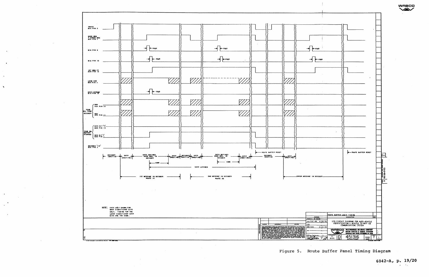
TRACK au PIN 2
8000 MSG + £RROR MSG 824 PIN t
811 PINS
811 PIN 10
tST MSQ FF 821 PIN 15
LEAO CAR 824 PIPf 4
T["" o. F'ROII
AU PIN
{
DBS
D£COOER 084
TENS NO. 8UFP'£R
AU PUf
130 PIN
i
14
II
.•. 15
{
BCD BIT
STORAGE ICD & IT 130 PIN
.. ,;
DECODED •1 o" 122 PIN 2
IHACTI r- DtCOD~~
70:: ~ - I.'.
v~ i. - L
~
i4- DATA ~· U"fOEFINEO
NOlE:. DATA oNLv SHOWN FOR MOST SIGNIFICANT BITS ONLY. TIUl'«J FOR THE LEAST SIGNIFICANT DATA BITS ARE THE SAM[ ..
:-1 u :l
I n I 1 I ~
20IIS 20jjS (
ous
·- 20jjS 2QIIS
I n I n ~ ~
-------------~ - -·
v~ z. /..
20IIS
~ [% ~ 7~ :c'. - ,I
~ ~ ~ /.. 7;z; ( ",-:'.
I :1
I n 1,.--. ROUTE BUFFER RESET 1--- ROUT£ BUFFER RESET
o:::.M.:.:~:. ==t~" .,J,!<-*' ~U ~ DATA D£Fl'£0 =r I DECODER DATAu1 INACTIVE GOOD MSG. IN DATA III re
UNDEFINED D[COOER UNOEF INC NACT IV£ NOEF INE OE CODER UNOE:F I NED
r=·Qa I- IDMS
DATA LATCH[O
IST ME'SSAK IN D!COD[Pt 1 I· 2NO MESSAGE Uf DECODER --1 ftOUTt 10 ROUTE 20
J I
-RROft. MESSAG£ IN DECODER
,-10-11
6-14-78
ROUTE BUFFER LOG IC TIUINB
STD CIRCUIT DIAGRAMS FOR AUTO-VEHICLE lfl:NTIFICATION ~ VEHICLE TO WAY' I[(
CO,MJNICATI~ ~~TEM
WABCO ~
WESTINGHOUSE Ml -E COIIPAIIY UNION SWITCH I SIGNAL DMSION 1WISSYAU POST PA. 15211 ~.
OIW
Figure 5. Route Buffer Panel Timing Diagram
6042-A, p. 19/20


8
H
F
E
-
-
B
-
I 1 I 6 i 5
~--~---- ~---------- -
SUFfJ)(. l""'D£"''"'°' MOLES P\..\JGG!.'D
PUI. VIC.W X>
·-------------.---------------~ (IRC.UIT DIAGRAM PER D\rJG
1-----+---.---ir--t-----------1------~--~--------;-----------------< -OZOI C. D E 04.51311- e,H.Ol Of, D451.3HO -Sl-t.0101. - 010"2.
-ozoz. C. ]) F D 451)11 · 5ff.O'l.01, 0201. 0451 3 lfo· .SH.O'tOf, ·02.0'L,- 0'203 . -·-!-----------------~
=:=:=i~=o=.,===~===1)=0==~=!==:=~=!=!1.=~=;=:.=-s=:=~:::.~:_:_t_~_o_z __ .-_11~~+~-:_: __ -z_fJ_1~_'_-:-=_~-=._s-~-;~-1-,~-~-:o=z=.=·=II='-="===·-==--... -_-:·_-_-_--:_--=_·--_·~~::~--------~-~
4 I
1~1·, I <I' •
,~~o m VIEWD
SlfO>l/li61tPPllcAT/(W{}F()PTICA/.J5dt.ATOl?S TO SPACE 51cFO,t;80(JPA QN- QZIH
•"" .. 0 ·~
3
• "';::J& • o••o~. O ll,1] 0
O j5, l'l O IM~RT ON.LY 00 MOT O i.i O SOLDER
I
0 ~· 0 ~I&, 0
v,e.w'"c· SHOW1N.6 APPLICl'-TIOt,l OF JUMPER ,-0
SPACE. IS C.RouP A Ot-t ·0'2.0'2
O O O I O
1N~S:RT ON\. Y 1 00 KOi
CATH00· 1·m-· 1 SOL PER
o.o VIEW"&"
SMO!tirrllNG APPLICA'TIOH OF. LEO'S TO 'SPACE 3,GROUP 8 G..i -0'2.0'2.
CATHODL~,·
~~f]~ -UJ5EIH 0'-'LY,PO
11 NOT 501.0L~
. V1E.W
0
A
51"\0WINC, APPLteA,TioN OF
L£.D'~ iO SPACE 20 o>-.i-0201
u-;- rlrlll flfffT;, .o ,~
VIEW -020'Z.
In r£srffli'SPYC£V· G.2;,:.
&::. TEST PER SPEC. E:U· 6/65
&. -r1=.~-r "OE.'Q. S,;.,&c. E....v·G.04-f
&. TE.ST PERSPC'C.£.U·f.048
3 2 I 1.::, j
i R~·-.. -.+ ...... -.-.~"fl"rJ'".~"'.·~ .. "' ... "' • ..---.-.sc:-.-.. -,-.• -.---+ .... -...,.-.. '--~-f_
I I. OJ 73'~ Pl>"E'-2 PER OTM£R TA6 r1oou L.ES H · f-':.+:.,::.:.:...o:.:..::;:.:.;..:..:.:.:::......,-1-'--"":.:C.,"'-"-----t+---t--t-f"-t • :'> 3. IJ 49ood= RI\IET Jlf PoP
t---++----+-t-··-+1,-+----------1-t---+---t-l~
! !
,..:"_.-+-' +-·-· ::.::.::.:1::.-::.::.::.-::,~::.::.:::.-::.-::.::.::.::.-::.-::.-::.::.::.::.::.::.::.::.::::.::.::.-___ -+_-+ ..... -t.....J l I •; , ,
(z) .,2.s OIA HOLES FoAVCC.
(Rt.F'ONt.Y)
I
VIEW - 0'2.0 I :-0203 t-0/04
(2) .125 ?HA, MOi-CS f"oA C,NO. (Rti:-.o,,.n.y)
G
F
-..._ E
--
D -
------_c
-0. ~ -"' V\ - .:,
- ~ "' -~
'"iL --~ B
&F~[QUENC'( 300 Hi!: #4St4/Z-tJ204 PANEt~A.SCD'.lliffOFAcE /A/,1 /:A/1\
&Rv&SER 5TAMP PART No.&:... C::MAAACT IERS i HIGH USING_ .. ,..-.,.-,..·..,.·"-K,...,V_·.,.· ..,340r-T' • .., ........ ..,....,.. ··N:..:4S=l-'-'4-"IZ=-·-0..:;
2.=o..:;
3-=-l-'-l'.'-'\<l.:..;N..:;£L= ... ·NT=Ee:RF.c,ll:.:C:..£-+'/"9'1\ll .... /.L=,t,,.~ ....... -------1~,: -
/J::::;,£E D451418 ·SH 0301 ~OR. T(A.Mlr,IAL LOc.ATtONS --. .,!"4'51412 -02.02 PANEL DECO~A: /i\/~ '3\ /5\. • NOTES: I I I I I I I 1 I I I I l N4S!,!~!;.!!.201 PRNE':.=!.u~ r.\._,">..!_...,._ ...... _
Figure 6. Route Buffer Panel Component Location
6042-A, p. 21/22


I