Embed Size (px)
Citation preview
Compact slit-based couplers formetal-dielectric-metal plasmonic
waveguides
Yin Huang,1,2 Changjun Min,2,3 and Georgios Veronis1,2,∗1Department of Electrical and Computer Engineering, Louisiana State University, Baton
Rouge, Louisiana 70803, USA2Center for Computation and Technology, Louisiana State University, Baton Rouge, Louisiana
70803, USA3Current address: Institute of Modern Optics, Nankai University, Tianjin 300071, China
Abstract: We introduce compact wavelength-scale slit-based structuresfor coupling free space light into metal-dielectric-metal (MDM) subwave-length plasmonic waveguides. We first show that for a single slit structurethe coupling efficiency is limited by a trade-off between the light powercoupled into the slit, and the transmission of the slit-MDM waveguidejunction. We next consider a two-section slit structure, and show thatfor such a structure the upper slit section enhances the coupling of theincident light into the lower slit section. The optimized two-section slitstructure results in ∼ 2.3 times enhancement of the coupling into the MDMplasmonic waveguide compared to the optimized single-slit structure. Wefinally consider a symmetric double-slit structure, and show that for sucha structure the surface plasmons excited at the metal-air interfaces arepartially coupled into the slits. Thus, the coupling of the incident light intothe slits is greatly enhanced, and the optimized double-slit structure resultsin ∼ 3.3 times coupling enhancement compared to the optimized single-slitstructure. In all cases the coupler response is broadband.
© 2012 Optical Society of America
OCIS codes: (240.6680) Surface plasmons; (260.3910) Metal optics; (130.2790) Guidedwaves.
References and links1. J. R. Krenn, B. Lamprecht, H. Ditlbacher, G. Schider, M. Salerno, A. Leitner, and F. R. Aussenegg, “Non-
diffraction-limited light transport by gold nanowires,” Europhys. Lett. 60, 663–669 (2002).2. S. A. Maier, P. G. Kik, H. A. Atwater, S. Meltzer, E. Harel, B. E. Koel, and A. A. G. Requicha, “Local detection
of electromagnetic energy transport below the diffraction limit in metal nanoparticle plasmon waveguides,” Nat.Mater. 2, 229–232 (2003).
3. S. I. Bozhevolnyi, V. S. Volkov, E. Devaux, J. Y. Laluet, and T. W. Ebbesen, “Channel plasmon subwavelengthwaveguide components including interferometers and ring resonators,” Nature 440, 508–511 (2006).
4. R. Zia, M. D. Selker, P. B. Catrysse, and M. L. Brongersma, “Geometries and materials for subwavelength surfaceplasmon modes,” J. Opt. Soc. Am. A 21, 2442–2446 (2004).
5. G. Veronis and S. Fan, “Bends and splitters in subwavelength metal-dielectric-metal plasmonic waveguides,”Appl. Phys. Lett. 87, 131102 (2005).
6. A. Hosseini and Y. Massoud, “Nanoscale surface plasmon based resonator using rectangular geometry,” Appl.Phys. Lett. 90, 181102 (2007).
7. Y. Matsuzaki, T. Okamoto, M. Haraguchi, M. Fukui, and M. Nakagaki, “Characteristics of gap plasmon waveg-uide with stub structures,” Opt. Express 16, 16314–16325 (2008).
#172962 - $15.00 USD Received 20 Jul 2012; revised 6 Sep 2012; accepted 7 Sep 2012; published 13 Sep 2012(C) 2012 OSA 24 September 2012 / Vol. 20, No. 20 / OPTICS EXPRESS 22233
8. X. S. Lin and X. G. Huang, “Tooth-shaped plasmonic waveguide filters with nanometeric sizes,” Opt. Lett. 33,2874–2876 (2008).
9. D. M. Pozar, Microwave Engineering (Wiley, New York, 1998).10. E. N. Economou, “Surface plasmons in thin films,” Phys. Rev. 182, 539–554 (1969).11. G. Veronis and S. Fan, “Theoretical investigation of compact couplers between dielectric slab waveguides and
two-dimensional metal-dielectric-metal plasmonic waveguides,” Opt. Express 15, 1211–1221 (2007).12. E. Feigenbaum and M. Orenstein, “Modeling of complementary void plasmon waveguiding,” J. Lightwave Tech-
nol. 25, 2547–2562 (2007).13. R. A. Wahsheh, Z. L. Lu, and M. A. G. Abushagur, “Nanoplasmonic couplers and splitters,” Opt. Express 17,
19033–19040 (2009).14. R. X. Yang, R. A. Wahsheh, Z. L. Lu, and M. A. G. Abushagur, “Efficient light coupling between dielectric slot
waveguide and plasmonic slot waveguide,” Opt. Lett. 35, 649–651 (2010).15. J. Tian, S. Yu, W. Yan, and M. Qiu, “Broadband high-efficiency surface-plasmon-polariton coupler with silicon-
metal interface,” Appl. Phys. Lett. 95, 013504 (2009).16. C. Delacour, S. Blaize, P. Grosse, J. M. Fedeli, A. Bruyant, R. Salas-Montiel, G. Lerondel, and A. Chelnokov,
“Efficient directional coupling between silicon and copper plasmonic nanoslot waveguides: toward metal-oxide-silicon nanophotonics,” Nano Lett. 10, 2922–2926 (2010).
17. M. J. Preiner, K. T. Shimizu, J. S. White, and N. A. Melosh, “Efficient optical coupling into metal-insulator-metalplasmon modes with subwavelength diffraction gratings,” Appl. Phys. Lett. 92, 113109 (2008).
18. J. A. Dionne, H. J. Lezec, and H. A. Atwater, “Highly confined photon transport in subwavelength metallic slotwaveguides,” Nano Lett. 6, 1928–1932 (2006).
19. H. J. Lezec, J. A. Dionne, and H. A. Atwater, “Negative refraction at visible frequencies,” Science 316, 430–432(2007).
20. S. I. Bozhevolnyi, Plasmonic Nanoguides and Circuits (World Scientific, 2009).21. P. Neutens, P. V. Dorpe, I. D. Vlaminck, L. Lagae, and G. Borghs, “Electrical detection of confined gap plasmons
in metal-insulator-metal waveguides,” Nature Photonics 3, 283–286 (2009).22. K. Diest, J. A. Dionne, M. Spain, and H. A. Atwater, “Tunable color filters based on metal-insulator-metal
resonators,” Nano Lett. 9, 2579–2583 (2009).23. S. D. Wu and E. N. Glytsis, “Finite-number-of-periods holographic gratings with finite-width incident beams:
analysis using the finite-difference frequency-domain method,” J. Opt. Soc. Am. A 19, 2018–2029 (2002).24. G. Veronis, R. W. Dutton, and S. Fan, “Method for sensitivity analysis of photonic crystal devices,” Opt. Lett.
29, 2288–2290 (2004).25. E. D. Palik, Handbook of Optical Constants of Solids (Academic, New York, 1985).26. J. Jin, The Finite Element Method in Electromagnetics (Wiley, New York, 2002).27. A. Taflove, Computational Electrodynamics (Artech House, Boston, 1995).28. S. E. Kocabas, G. Veronis, D. A. B. Miller, and S. Fan, “Transmission line and equivalent circuit models for
plasmonic waveguide components,” IEEE J. Sel. Topics Quantum Electron. 14, 1462–1472 (2008).29. S. Ramo, J. R. Whinnery, and T. Van Duzer, Fields and Waves in Communication Electronics (Wiley, New York,
1994).30. C. Min and G. Veronis, “Absorption switches in metal-dielectric-metal plasmonic waveguides,” Opt. Express 17,
10757–10766 (2009).31. K. Krishnakumar, “Micro-genetic algorithms for stationary and non-stationary function optimization,” Proc.
SPIE 1196, 289–296 (1989).32. C. Min, L. Yang, and G. Veronis, “Microcavity enhanced optical absorption in subwavelength slits,” Opt. Express
19, 26850–26858 (2011).33. L. Verslegers, Z. Yu, P. B. Catrysse, and S. Fan, “Temporal coupled-mode theory for resonant apertures,” J. Opt.
Soc. Am. B 27, 1947–1956 (2010).34. C. A. Balanis, Antenna Theory: Analysis and Design, 3rd ed. (Wiley, 2005).
1. Introduction
Plasmonic waveguides have shown the potential to guide subwavelength optical modes, theso-called surface plasmon polaritons, at metal-dielectric interfaces. Several different nanoscaleplasmonic waveguiding structures have been proposed, such as metallic nanowires, metallicnanoparticle arrays, V-shaped grooves, and metal-dielectric-metal (MDM) waveguides [1–8].Among these, MDM plasmonic waveguides, which are the optical analogue of microwave two-conductor transmission lines [9], are of particular interest because they support modes withdeep subwavelength scale over a very wide range of frequencies extending from DC to visi-ble [10]. Thus, MDM waveguides could provide an interface between conventional optics and
#172962 - $15.00 USD Received 20 Jul 2012; revised 6 Sep 2012; accepted 7 Sep 2012; published 13 Sep 2012(C) 2012 OSA 24 September 2012 / Vol. 20, No. 20 / OPTICS EXPRESS 22234
subwavelength electronic and optoelectronic devices.For applications involving MDM plasmonic waveguides, it is essential to develop compact
structures to couple light efficiently into such waveguides [11]. Several different couplers be-tween MDM and dielectric waveguides have been investigated both theoretically and experi-mentally [11–16]. In addition, structures for coupling free space radiation into MDM waveg-uides have also been investigated. In particular, Preiner et al. [17] investigated subwavelengthdiffraction gratings as coupling structures into MDM waveguide modes. However, in diffractiongrating structures several grating periods are required for efficient waveguide mode excitation,so that such structures need to be several microns long when designed to operate at frequenciesaround the optical communication wavelength (λ0 =1.55 μm). In addition, in several experi-mental investigations of MDM waveguides and devices, a single slit was used to couple lightfrom free space into MDM plasmonic waveguides [18–22]. While single slit coupling structuresare more compact, slit-based coupler designs have not been investigated in detail.
In this paper, we investigate compact wavelength-scale slit-based structures for coupling freespace light into MDM plasmonic waveguides. We show that for a single slit structure the cou-pling efficiency is limited by a trade-off between the light power coupled into the slit, and thetransmission of the slit-MDM waveguide junction. We next consider a two-section slit structure,and show that for such a structure the upper slit section enhances the coupling of the incidentlight into the lower slit section, by improving the impedance matching between the incidentplane wave and the lower slit mode. The optimized two-section slit structure results in ∼ 2.3times enhancement of the coupling into the MDM plasmonic waveguide compared to the op-timized single-slit structure. We then consider a symmetric double-slit structure. We show thatfor such a structure the surface plasmons excited at the metal-air interfaces are partially coupledinto the slits, and thus the coupling of the incident light into the slits is greatly enhanced. Theoptimized double-slit structure results in ∼ 3.3 times coupling enhancement compared to theoptimized single-slit structure. Finally, we show that, while all incoupling structures are opti-mized at a single wavelength, the operation wavelength range for high coupling efficiency isbroad.
The remainder of the paper is organized as follows. In Section 2, we first define the transmis-sion cross section of the MDM plasmonic waveguide for a given coupling structure, and brieflydescribe the simulation method used for the analysis of the couplers. The results obtained forthe single slit, two-section slit, and double slit coupling structures are presented in Subsections2.1, 2.2, and 2.3, respectively. Finally, our conclusions are summarized in Section 3.
2. Results
We consider a silver-silica-silver MDM plasmonic waveguide in which the upper metal layerhas a finite thickness (Fig. 1(a)). The minimum thickness of this metal layer is chosen to be 150nm. For such a thickness, the field profile and wave vector of the fundamental TM mode sup-ported by such a waveguide at optical frequencies are essentially identical to the ones of a MDMplasmonic waveguide with semi-infinite metal layers. We consider compact wavelength-scalestructures for incoupling a normally incident plane wave from free space into the fundamentalmode of the silver-silica-silver MDM plasmonic waveguide. In all cases, the total width of theincoupling structure is limited to less than 1.1μm, which approximately corresponds to onewavelength in silica (λs = λ0/ns, where ns =1.44), when operating at the optical communica-tion wavelength (λ0 =1.55 μm).
Due to the symmetry of all coupling structures considered in this paper, the same amount ofpower couples into the left and right propagating silver-silica-silver MDM waveguide modes.In other words, half of the total incoupled power couples into each of the left and right propagat-ing MDM waveguide modes. For comparison of different incoupling configurations, we define
#172962 - $15.00 USD Received 20 Jul 2012; revised 6 Sep 2012; accepted 7 Sep 2012; published 13 Sep 2012(C) 2012 OSA 24 September 2012 / Vol. 20, No. 20 / OPTICS EXPRESS 22235
the transmission cross section σT of the silver-silica-silver MDM waveguide as the total lightpower coupled into the right propagating fundamental TM mode of the waveguide, normalizedby the incident plane wave power flux density [11]. In two dimensions, the transmission crosssection is in the unit of length.
We use a two-dimensional finite-difference frequency-domain (FDFD) method [23, 24] tonumerically calculate the transmission in the MDM plasmonic waveguide. This method allowsus to directly use experimental data for the frequency-dependent dielectric constant of metalssuch as silver [25], including both the real and imaginary parts, with no approximation. Per-fectly matched layer (PML) absorbing boundary conditions are used at all boundaries of thesimulation domain [26]. We also use the total-field-scattered-field formulation to simulate theresponse of the structure to a normally incident plane wave input [27].
2.1. Single slit coupler
Fig. 1. (a) Schematic of a structure consisting of a single slit for incoupling a normallyincident plane wave from free space into the fundamental mode of a MDM plasmonicwaveguide. (b) Transmission cross section σT of the MDM plasmonic waveguide in units ofw for the structure of Fig. 1(a) as a function of the slit width d and length h calculated usingFDFD. Results are shown for a silver-silica-silver structure with w = 50 nm at λ0 =1.55μm. (c) Transmission cross section σT for the structure of Fig. 1(a) as a function of theslit length h calculated using FDFD (red circles) and scattering matrix theory (black solidline). Results are shown for d = 220 nm. All other parameters are as in Fig. 1(b). (d) Profileof the magnetic field amplitude for the structure of Fig. 1(a) for d = 250 nm and h = 205nm, normalized with respect to the field amplitude of the incident plane wave. All otherparameters are as in Fig. 1(b).
We first consider a structure consisting of a single slit for incoupling a normally incident
#172962 - $15.00 USD Received 20 Jul 2012; revised 6 Sep 2012; accepted 7 Sep 2012; published 13 Sep 2012(C) 2012 OSA 24 September 2012 / Vol. 20, No. 20 / OPTICS EXPRESS 22236
plane wave from free space into the fundamental mode of the silver-silica-silver MDM plas-monic waveguide with dielectric core thickness w. The slit extends half way into the dielectriccore of the MDM waveguide (Fig. 1(a)). In Fig. 1(b), we show the transmission cross sectionσT of the silver-silica-silver MDM waveguide in units of w for the single slit structure of Fig.1(a) as a function of the width d and length h of the slit. For the range of parameters shown,we observe one transmission peak. The maximum cross section of σT ∼ 4.67w is obtained forsuch an incoupling structure at d = 250 nm and h = 205 nm (Fig. 1(b)).
Both the silver-silica-silver MDM waveguide and the silver-air-silver slit have subwave-length widths, so that only the fundamental TM mode is propagating in them. Thus, we canuse single-mode scattering matrix theory to account for the behavior of the system [28]. Weuse FDFD to numerically extract the transmission cross section σT1 of a silver-air-silver MDMwaveguide with air core thickness d (Fig. 2(a)). We also use FDFD to extract the complex mag-netic field reflection coefficient r1 and transmission coefficient t1 of the fundamental mode ofa silver-air-silver MDM waveguide at the T-shaped junction with a silver-silica-silver MDMwaveguide (Fig. 2(b)), as well as the reflection coefficient r2 at the interface between the silver-air-silver MDM waveguide and air (Fig. 2(c)).
Fig. 2. (a) Schematic defining the transmission cross section σT1 of a semi-infinite MDMwaveguide when a plane wave is normally incident on it. (b) Schematic defining the re-flection coefficient r1, and transmission coefficient t1 when the fundamental TM mode of ametal-air-metal waveguide is incident at the junction with a metal-dielectric-metal waveg-uide. (c) Schematic defining the reflection coefficient r2 of the fundamental TM mode ofa MDM waveguide at the waveguide/air interface. (d) Schematic defining the transmissioncross section σT2 of two semi-infinite MDM waveguides when a plane wave is normallyincident on them. (e) Schematic defining the reflection coefficient r3, and transmission co-efficients t2, t3 when the fundamental TM mode of a metal-dielectric-metal waveguide isincident at the junction with a metal-air-metal waveguide. (f) Schematic of a structure con-sisting of two semi-infinite MDM waveguides defining the reflection coefficient r4 of thefundamental TM mode of one of the MDM waveguides at the waveguide/air interface, andthe transmission coefficient t4 into the other MDM waveguide.
The transmission cross section σT of the silver-silica-silver MDM waveguide for the singleslit structure of Fig. 1(a) can then be calculated using scattering matrix theory as [28]:
σT = σT1ηres1Tsplitter, (1)
where Tsplitter=|t1|2 is the power transmission coefficient of the T-shaped junction of Fig. 2(b),
#172962 - $15.00 USD Received 20 Jul 2012; revised 6 Sep 2012; accepted 7 Sep 2012; published 13 Sep 2012(C) 2012 OSA 24 September 2012 / Vol. 20, No. 20 / OPTICS EXPRESS 22237
ηres1 = | exp(−γ1h)1−r1r2 exp(−2γ1h) |2 is the resonance enhancement factor associated with the silver-air-
silver slit resonance, and γ1 = α1 + iβ1 is the complex wave vector of the fundamental propa-gating TM mode in a silver-air-silver MDM waveguide with air core thickness d. We note thatηres1 is a function of the reflection coefficients r1 and r2 at both sides of the silver-air-silverslit. We also observe that the resonance enhancement factor ηres1 exhibits a maximum when theslit Fabry-Perot resonance condition arg(r1)+ arg(r2)−2β1h =−2mπ is satisfied, where m isan integer. Thus, for a given silver-air-silver slit width d, the transmission cross section σT ofthe silver-silica-silver MDM waveguide is maximized for slit lengths h which satisfy the aboveFabry-Perot resonance condition.
In Fig. 1(c), we show the transmission cross section σT of the silver-silica-silver MDMwaveguide for the single slit structure of Fig. 1(a) as a function of the slit length h calculatedusing FDFD. We observe that, as the slit length h increases, the transmission cross section σT
exhibits peaks, corresponding to the Fabry-Perot resonances in the slit. The maximum transmis-sion cross section σT is obtained at the first peak associated with the first Fabry-Perot resonancein the slit. In Fig. 1(c), we also show σT calculated using scattering matrix theory (Eq. (1)). Weobserve that there is excellent agreement between the scattering matrix theory results and theexact results obtained using FDFD.
For the optimized single slit structure (d = 250 nm, h = 205 nm), the transmission cross sec-tion σT1 of the corresponding silver-air-silver MDM waveguide with air core thickness d = 250nm (Fig. 2(a)) is ∼ 7.71w = 385.5 nm (Table 1). In other words, the silver-air-silver subwave-length MDM waveguide collects light from an area significantly larger than its geometric cross-sectional area [11]. In addition, for the optimized single slit structure the power transmissioncoefficient of the T-shaped junction is Tsplitter ∼0.37, and the resonance enhancement factor isηres1 ∼1.64 (Table 1). Thus, ∼ 2×37= 74% of the incident power at the junction is transmittedto the left and right propagating modes of the silver-silica-silver MDM waveguide.
Fig. 3. Transmission cross sections (in units of w = 50 nm) of a single silver-air-silverMDM waveguide σT1 (Fig. 2(a)), and of a double silver-air-silver MDM waveguide σT2
(Fig. 2(d)), as a function of their total air core thickness (d for the single and 2d for thedouble waveguide). The total width of the double waveguide is 2d+D = 1.1μm.
In Fig. 3, we show the transmission cross section σT1 of a silver-air-silver MDM waveguide(Fig. 2(a)) as a function of the waveguide air core thickness d. We observe that, as expected, σT1
increases monotonically as the thickness d increases. In other words, the light power collectedby the waveguide increases as the air core thickness of the waveguide increases. On the otherhand, the properties of the T-shaped junction (Fig. 2(b)) can be described using the conceptof characteristic impedance and transmission line theory [5, 9, 29]. Based on transmission line
#172962 - $15.00 USD Received 20 Jul 2012; revised 6 Sep 2012; accepted 7 Sep 2012; published 13 Sep 2012(C) 2012 OSA 24 September 2012 / Vol. 20, No. 20 / OPTICS EXPRESS 22238
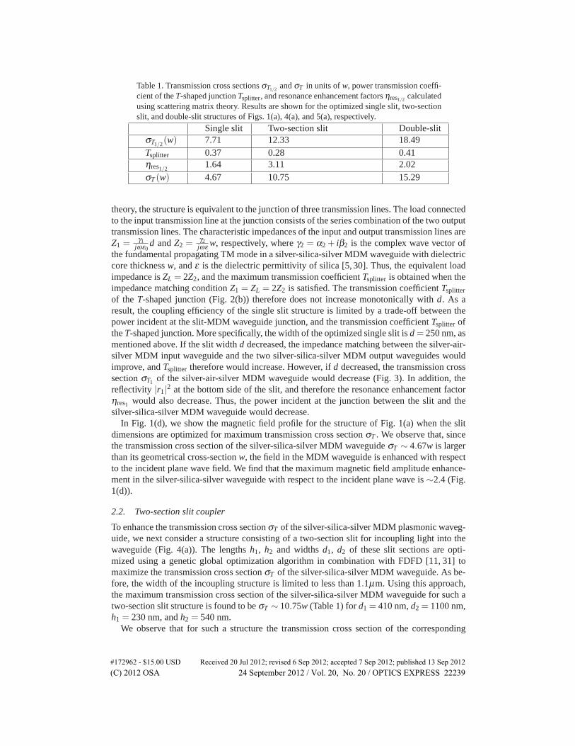
Table 1. Transmission cross sections σT1/2 and σT in units of w, power transmission coeffi-cient of the T-shaped junction Tsplitter, and resonance enhancement factors ηres1/2 calculatedusing scattering matrix theory. Results are shown for the optimized single slit, two-sectionslit, and double-slit structures of Figs. 1(a), 4(a), and 5(a), respectively.
Single slit Two-section slit Double-slitσT1/2
(w) 7.71 12.33 18.49Tsplitter 0.37 0.28 0.41ηres1/2
1.64 3.11 2.02σT (w) 4.67 10.75 15.29
theory, the structure is equivalent to the junction of three transmission lines. The load connectedto the input transmission line at the junction consists of the series combination of the two outputtransmission lines. The characteristic impedances of the input and output transmission lines areZ1 =
γ1jωε0
d and Z2 =γ2
jωε w, respectively, where γ2 = α2 + iβ2 is the complex wave vector ofthe fundamental propagating TM mode in a silver-silica-silver MDM waveguide with dielectriccore thickness w, and ε is the dielectric permittivity of silica [5, 30]. Thus, the equivalent loadimpedance is ZL = 2Z2, and the maximum transmission coefficient Tsplitter is obtained when theimpedance matching condition Z1 = ZL = 2Z2 is satisfied. The transmission coefficient Tsplitter
of the T-shaped junction (Fig. 2(b)) therefore does not increase monotonically with d. As aresult, the coupling efficiency of the single slit structure is limited by a trade-off between thepower incident at the slit-MDM waveguide junction, and the transmission coefficient Tsplitter ofthe T-shaped junction. More specifically, the width of the optimized single slit is d = 250 nm, asmentioned above. If the slit width d decreased, the impedance matching between the silver-air-silver MDM input waveguide and the two silver-silica-silver MDM output waveguides wouldimprove, and Tsplitter therefore would increase. However, if d decreased, the transmission crosssection σT1 of the silver-air-silver MDM waveguide would decrease (Fig. 3). In addition, thereflectivity |r1|2 at the bottom side of the slit, and therefore the resonance enhancement factorηres1 would also decrease. Thus, the power incident at the junction between the slit and thesilver-silica-silver MDM waveguide would decrease.
In Fig. 1(d), we show the magnetic field profile for the structure of Fig. 1(a) when the slitdimensions are optimized for maximum transmission cross section σT . We observe that, sincethe transmission cross section of the silver-silica-silver MDM waveguide σT ∼ 4.67w is largerthan its geometrical cross-section w, the field in the MDM waveguide is enhanced with respectto the incident plane wave field. We find that the maximum magnetic field amplitude enhance-ment in the silver-silica-silver waveguide with respect to the incident plane wave is ∼2.4 (Fig.1(d)).
2.2. Two-section slit coupler
To enhance the transmission cross section σT of the silver-silica-silver MDM plasmonic waveg-uide, we next consider a structure consisting of a two-section slit for incoupling light into thewaveguide (Fig. 4(a)). The lengths h1, h2 and widths d1, d2 of these slit sections are opti-mized using a genetic global optimization algorithm in combination with FDFD [11, 31] tomaximize the transmission cross section σT of the silver-silica-silver MDM waveguide. As be-fore, the width of the incoupling structure is limited to less than 1.1μm. Using this approach,the maximum transmission cross section of the silver-silica-silver MDM waveguide for such atwo-section slit structure is found to be σT ∼ 10.75w (Table 1) for d1 = 410 nm, d2 = 1100 nm,h1 = 230 nm, and h2 = 540 nm.
We observe that for such a structure the transmission cross section of the corresponding
#172962 - $15.00 USD Received 20 Jul 2012; revised 6 Sep 2012; accepted 7 Sep 2012; published 13 Sep 2012(C) 2012 OSA 24 September 2012 / Vol. 20, No. 20 / OPTICS EXPRESS 22239
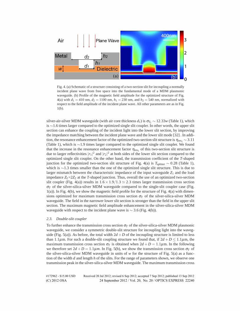
Fig. 4. (a) Schematic of a structure consisting of a two-section slit for incoupling a normallyincident plane wave from free space into the fundamental mode of a MDM plasmonicwaveguide. (b) Profile of the magnetic field amplitude for the optimized structure of Fig.4(a) with d1 = 410 nm, d2 = 1100 nm, h1 = 230 nm, and h2 = 540 nm, normalized withrespect to the field amplitude of the incident plane wave. All other parameters are as in Fig.1(b).
silver-air-silver MDM waveguide (with air core thickness d1) is σT1 ∼ 12.33w (Table 1), whichis ∼1.6 times larger compared to the optimized single slit coupler. In other words, the upper slitsection can enhance the coupling of the incident light into the lower slit section, by improvingthe impedance matching between the incident plane wave and the lower slit mode [32] . In addi-tion, the resonance enhancement factor of the optimized two-section slit structure is ηres1 ∼ 3.11(Table 1), which is ∼1.9 times larger compared to the optimized single slit coupler. We foundthat the increase in the resonance enhancement factor ηres1 of this two-section slit structure isdue to larger reflectivities |r1|2 and |r2|2 at both sides of the lower slit section compared to theoptimized single slit coupler. On the other hand, the transmission coefficient of the T-shapedjunction for the optimized two-section slit structure of Fig. 4(a) is Tsplitter ∼ 0.28 (Table 1),which is ∼1.3 times smaller than the one of the optimized single slit structure. This is due tolarger mismatch between the characteristic impedance of the input waveguide Z1 and the loadimpedance ZL=2Z2 at the T-shaped junction. Thus, overall the use of an optimized two-sectionslit coupler (Fig. 4(a)) results in 1.6× 1.9/1.3 � 2.3 times larger transmission cross sectionσT of the silver-silica-silver MDM waveguide compared to the single-slit coupler case (Fig.1(a)). In Fig. 4(b), we show the magnetic field profile for the structure of Fig. 4(a) with dimen-sions optimized for maximum transmission cross section σT of the silver-silica-silver MDMwaveguide. The field in the narrower lower slit section is stronger than the field in the upper slitsection. The maximum magnetic field amplitude enhancement in the silver-silica-silver MDMwaveguide with respect to the incident plane wave is ∼ 3.6 (Fig. 4(b)).
2.3. Double-slit coupler
To further enhance the transmission cross section σT of the silver-silica-silver MDM plasmonicwaveguide, we consider a symmetric double-slit structure for incoupling light into the waveg-uide (Fig. 5(a)). As before, the total width 2d +D of the incoupling structure is limited to lessthan 1.1μm. For such a double-slit coupling structure we found that, if 2d +D ≤ 1.1μm, themaximum transmission cross section σT is obtained when 2d +D = 1.1μm. In the followingwe therefore set 2d +D = 1.1μm. In Fig. 5(b), we show the transmission cross section σT ofthe silver-silica-silver MDM waveguide in units of w for the structure of Fig. 5(a) as a func-tion of the width d and length h of the slits. For the range of parameters shown, we observe onetransmission peak in the silver-silica-silver MDM waveguide. The maximum transmission cross
#172962 - $15.00 USD Received 20 Jul 2012; revised 6 Sep 2012; accepted 7 Sep 2012; published 13 Sep 2012(C) 2012 OSA 24 September 2012 / Vol. 20, No. 20 / OPTICS EXPRESS 22240
Fig. 5. (a) Schematic of a double-slit structure for incoupling a normally incident planewave from free space into the fundamental mode of a MDM plasmonic waveguide. (b)Transmission cross section σT of the MDM plasmonic waveguide in units of w for thestructure of Fig. 5(a) as a function of the slit width d and length h calculated using FDFD.The total width of the incoupling structure is 2d+D = 1.1μm. All other parameters are asin Fig. 1(b). (c) Transmission cross section σT for the structure of Fig. 5(a) as a functionof the slit length h calculated using FDFD (red circles) and scattering matrix theory (blacksolid line). Results are shown for d = 220 nm. All other parameters are as in Fig. 5(b). (d)Profile of the magnetic field amplitude for the structure of Fig. 5(a) for d = 200 nm andh = 250 nm, normalized with respect to the field amplitude of the incident plane wave. Allother parameters are as in Fig. 5(b).
section of σT ∼ 15.29w is obtained for such an incoupling structure at d = 200 nm (D = 700nm) and h = 250 nm. We also note that for d ∼ 400 nm (D ∼ 300 nm) the transmission intothe silver-silica-silver MDM waveguide is almost zero (Fig. 5(b)). We found that this is dueto the fact that for a slit distance of D ∼ 300 nm the incident light strongly couples into thesilver-silica-silver waveguide resonator between the slits. In addition, there is almost no lightcoupled into the left and right propagating modes of the silver-silica-silver MDM waveguide,due to destructive interference between the wave directly coupled through the slit, and the wavecoupled through the silver-silica-silver waveguide resonator.
We use again single-mode scattering matrix theory to account for the behavior of the system.We use FDFD to numerically extract the transmission cross section σT2 of a double silver-air-silver MDM waveguide as in Fig. 2(d). We also use FDFD to extract the complex magneticfield reflection coefficient r3 and transmission coefficients t2, t3 of the fundamental mode ofa silver-silica-silver MDM waveguide at the T-shaped junction with a silver-air-silver MDMwaveguide (Fig. 2(e)). Note that t1 = t2 due to reciprocity [9]. Finally, we also extract the re-
#172962 - $15.00 USD Received 20 Jul 2012; revised 6 Sep 2012; accepted 7 Sep 2012; published 13 Sep 2012(C) 2012 OSA 24 September 2012 / Vol. 20, No. 20 / OPTICS EXPRESS 22241
flection coefficient r4 at the interface between the silver-air-silver MDM waveguide and air, andthe transmission coefficient t4 into the other MDM waveguide, for the double MDM waveguidestructure (Fig. 2(f)). The transmission cross section σT of the silver-silica-silver MDM plas-monic waveguide for the double-slit coupling structure of Fig. 5(a) is then calculated usingscattering matrix theory as:
σT = σT2ηres2Tsplitter, (2)
where, as before, Tsplitter = |t1|2 = |t2|2 is the power transmission coefficient of the T-shaped
junction, ηres2 = | exp(−γ1h)(1+t3A)1−(r1+t1t2A)(r4+t4)exp(−2γ1h) |2 is the resonance enhancement factor associated
with the complex resonator formed by the two silver-air-silver slits and the silver-silica-silverMDM waveguide resonator of length D between them, and A = exp(−γ2D)+r3 exp(−2γ2D)
1−r23 exp(−2γ2D)
. Thus,
we observe that the resonant enhancement factor ηres2 for such a complex resonator is similar tothat of a Fabry-Perot resonator with effective reflectivities reff1 = r1 + t1t2A and reff2 = r4 + t4.
In Fig. 5(c), we show the transmission cross section σT for the structure of Fig. 5(a) asa function of the slit length h calculated using FDFD. We observe that, as the slit length hincreases, the transmission cross section σT exhibits peaks, associated with the resonancesof the double-slit structure. The maximum transmission cross section σT is obtained at thefirst peak associated with the first resonant length of the slits. In Fig. 5(c), we also show σT
calculated using scattering matrix theory (Eq. (2)). We observe that there is excellent agreementbetween the scattering matrix theory results and the exact results obtained using FDFD.
We found that for the optimized double-slit structure the transmission cross section of thecorresponding double silver-air-silver MDM waveguide (Fig. 2(d)) is σT2 ∼ 18.49w (Table 1),which is ∼2.4 times larger compared to the transmission cross section σT1 ∼ 7.71w of the singlesilver-air-silver MDM waveguide corresponding to the optimized single slit coupler (Fig. 2(a)).In Fig. 3 we show the transmission cross sections of a single silver-air-silver MDM waveguideσT1 (Fig. 2(a)), and of a double silver-air-silver MDM waveguide σT2 (Fig. 2(d)) as a functionof their total air core thickness (d for the single and 2d for the double waveguide). We observethat a double silver-air-silver MDM waveguide collects more light than a single silver-air-silverMDM waveguide with the same total air core thickness. This is due to the fact that, when aplane wave is incident on a semi-infinite MDM waveguide, surface plasmon waves are excitedat the air-metal interfaces. In the double MDM waveguide structure (Fig. 2(d)), the power ofthese surface plasmon waves is partially coupled into the MDM waveguides, thus increasingthe total light power collected by the structure. In addition, the resonance enhancement factorof the optimized double-slit structure ηres2 ∼ 2.02 (Table 1) is slightly larger than the resonanceenhancement factor of the optimized single slit coupler (ηres1 ∼ 1.64). Overall, the use of anoptimized double-slit coupler (Fig. 5(a)) results in ∼ 3.3 times larger transmission cross sectionσT of the silver-silica-silver MDM waveguide compared to the optimized single-slit couplercase (Fig. 1(a)). In Fig. 5(d), we show the magnetic field profile for the structure of Fig. 5(a)with dimensions optimized for maximum transmission cross section. The maximum magneticfield amplitude enhancement in the silver-silica-silver waveguide with respect to the incidentplane wave is ∼ 4.2.
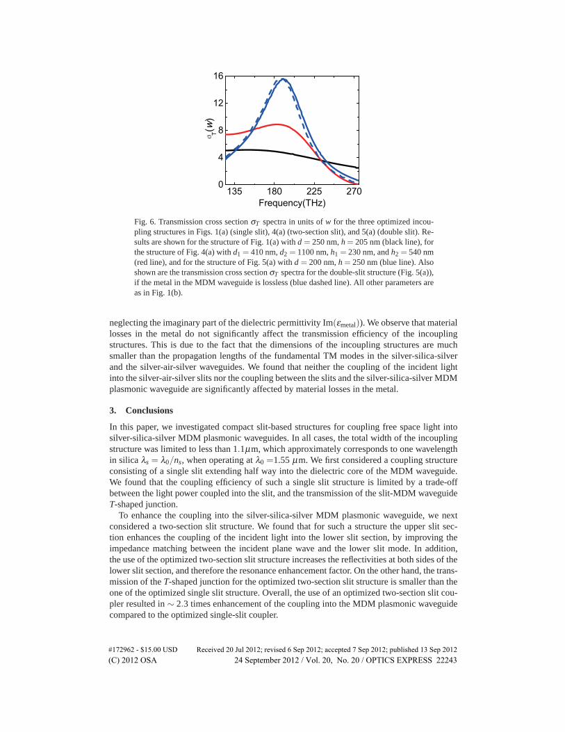
The incoupling structures were all optimized at a single wavelength of λ0 =1.55 μm. InFig. 6, we show the transmission cross section σT of the silver-silica-silver MDM plasmonicwaveguide as a function of frequency for the optimized structures of Fig. 1(d) (single slit),Fig. 4(b) (two-section slit), and Fig. 5(d) (double slit). We observe that the operation frequencyrange for high transmission is broad. This is due to the fact that in all cases the enhancedtransmission is not associated with any strong resonances. In other words, the quality factors Qof the slit coupling structures are low. In Fig. 6 we also show the transmission cross section σT
for the double-slit structure, if the metal in the MDM waveguide is lossless (εmetal = Re(εmetal),
#172962 - $15.00 USD Received 20 Jul 2012; revised 6 Sep 2012; accepted 7 Sep 2012; published 13 Sep 2012(C) 2012 OSA 24 September 2012 / Vol. 20, No. 20 / OPTICS EXPRESS 22242
135 180 225 2700
4
8
12
16
T(w
)
Frequency(THz)
Fig. 6. Transmission cross section σT spectra in units of w for the three optimized incou-pling structures in Figs. 1(a) (single slit), 4(a) (two-section slit), and 5(a) (double slit). Re-sults are shown for the structure of Fig. 1(a) with d = 250 nm, h = 205 nm (black line), forthe structure of Fig. 4(a) with d1 = 410 nm, d2 = 1100 nm, h1 = 230 nm, and h2 = 540 nm(red line), and for the structure of Fig. 5(a) with d = 200 nm, h = 250 nm (blue line). Alsoshown are the transmission cross section σT spectra for the double-slit structure (Fig. 5(a)),if the metal in the MDM waveguide is lossless (blue dashed line). All other parameters areas in Fig. 1(b).
neglecting the imaginary part of the dielectric permittivity Im(εmetal)). We observe that materiallosses in the metal do not significantly affect the transmission efficiency of the incouplingstructures. This is due to the fact that the dimensions of the incoupling structures are muchsmaller than the propagation lengths of the fundamental TM modes in the silver-silica-silverand the silver-air-silver waveguides. We found that neither the coupling of the incident lightinto the silver-air-silver slits nor the coupling between the slits and the silver-silica-silver MDMplasmonic waveguide are significantly affected by material losses in the metal.
3. Conclusions
In this paper, we investigated compact slit-based structures for coupling free space light intosilver-silica-silver MDM plasmonic waveguides. In all cases, the total width of the incouplingstructure was limited to less than 1.1μm, which approximately corresponds to one wavelengthin silica λs = λ0/ns, when operating at λ0 =1.55 μm. We first considered a coupling structureconsisting of a single slit extending half way into the dielectric core of the MDM waveguide.We found that the coupling efficiency of such a single slit structure is limited by a trade-offbetween the light power coupled into the slit, and the transmission of the slit-MDM waveguideT-shaped junction.
To enhance the coupling into the silver-silica-silver MDM plasmonic waveguide, we nextconsidered a two-section slit structure. We found that for such a structure the upper slit sec-tion enhances the coupling of the incident light into the lower slit section, by improving theimpedance matching between the incident plane wave and the lower slit mode. In addition,the use of the optimized two-section slit structure increases the reflectivities at both sides of thelower slit section, and therefore the resonance enhancement factor. On the other hand, the trans-mission of the T-shaped junction for the optimized two-section slit structure is smaller than theone of the optimized single slit structure. Overall, the use of an optimized two-section slit cou-pler resulted in ∼ 2.3 times enhancement of the coupling into the MDM plasmonic waveguidecompared to the optimized single-slit coupler.
#172962 - $15.00 USD Received 20 Jul 2012; revised 6 Sep 2012; accepted 7 Sep 2012; published 13 Sep 2012(C) 2012 OSA 24 September 2012 / Vol. 20, No. 20 / OPTICS EXPRESS 22243
To further enhance the coupling into the silver-silica-silver MDM plasmonic waveguide, weconsidered a symmetric double-slit structure. We found that such a structure greatly enhancesthe coupling of the incident light into the slits. This is due to the fact that the incident lightexcites surface plasmons at the air-metal interfaces. In the case of a double-slit structure theseplasmons are partially coupled into the slits, thus increasing the total light power collected bythe structure. In addition, the resonance enhancement factor of the optimized double-slit coupleris slightly larger than the resonance enhancement factor of the optimized single slit coupler.Overall, the use of an optimized double-slit coupler resulted in ∼ 3.3 times enhancement of thecoupling into the MDM plasmonic waveguide compared to the optimized single-slit coupler.We also found that, while the incoupling structures were all optimized at a single wavelength,the operation wavelength range for high coupling efficiency is broad.
As final remarks, for wavelength-scale slit-based structures the double-slit structure results inoptimal coupling performance. We verified that, if three or more slits are used in a wavelength-scale coupler, the performance is always worse due to destructive interference between thewaves coupled through the slits. Moreover, if a reflector is introduced in one of the two silver-silica-silver MDM output waveguides, then all the incoupled power will couple into the othersilver-silica-silver MDM output waveguide. In addition, the proposed slit-based structures canalso be used to couple light from a MDM plasmonic waveguide into free space. We found that,when the single slit structure is used to outcouple light, the radiation pattern of the structure isapproximately isotropic [33]. On the other hand, we found that the two-section slit and double-slit structures introduce anisotropy in the radiation pattern, with stronger radiation in the normaldirection [33]. Finally, we note that there are some analogies between the proposed couplingstructures and the slot antennas used in the microwave frequency range [34].
Acknowledgments
This research was supported by the Louisiana Board of Regents (contracts LEQSF(2009-12)-RD-A-08 and LEQSF-EPS(2012)-PFUND-281), and the National Science Foundation (AwardNo. 1102301).
#172962 - $15.00 USD Received 20 Jul 2012; revised 6 Sep 2012; accepted 7 Sep 2012; published 13 Sep 2012(C) 2012 OSA 24 September 2012 / Vol. 20, No. 20 / OPTICS EXPRESS 22244