Embed Size (px)
Citation preview
HV-DC
TIDA-01160
12 V 15 V
PWM
±8 V
3.3 V
LM25017Synchronous
DC-DC Converter
Switching Node
EN-PWM
Copyright © 2017, Texas Instruments Incorporated
UCC53x0Isolated Gate
Driver
1TIDUCV0–June 2017Submit Documentation Feedback
Copyright © 2017, Texas Instruments Incorporated
Compact, Single-Channel, Isolated Gate Drive Reference Design for UPSand Inverters
TI Designs: TIDA-01160Compact, Single-Channel, Isolated Gate Drive ReferenceDesign for UPS and Inverters
DescriptionThe TIDA-01160 design provides a reference solutionfor high-side or low-side isolated gate drivers used indriving power stages of UPS, inverters, and chargepile applications.
This TI Design is based on the UCC5320S3-kVRMS basic isolated gate driver for driving IGBTsand SiC MOSFETs. The reference design contains abuilt-in compact, 1.5-W, isolated Fly-Buck™ gatedriver power supply for powering the input and outputof the isolated gate driver.
By bringing together the isolated gate driver andisolated gate driver power supply in a compact boardwith a form factor of 33 mm × 23 mm, this referencedesign provides a fully tested, robust, independent,easy to validate, single-channel driver solution,capable of withstanding > 100-kV/µs CMTI.
Resources
TIDA-01160 Design FolderUCC5320S Product FolderLM25017 Product Folder
ASK Our E2E Experts
Features• Suited for Single- and Three-Phase Inverters,
Mid- and High-Voltage Power Converters(100- to 230-V AC)
• 0.5-A/2-A/6-A/10-A Source and Sink Current SuitsDriving MOSFET, IGBT, SiC-FET With Currents upto 100 A and Operating Frequencies up to 500 kHz
• Protection Against Spurious Turnon and Turnoff ofIGBT and FET During Power-on and Power-offSequences
• 4000-VPK and 2500-VRMS Isolation Barrier• Driver Solution Validated and Meets High Common
Mode Transient Immunity (CMTI) of > 100 kV/µs• Built-in Low-Cost, Low-Component, Compact
Isolated Gate Driver Power Supply to Power High-Voltage Side Circuit With Negative Bias for NoiseImmunity
• Compact, Small Form Factor (33-mm×23-mm)Gate Drive Solution
• Easy Interface With Both Digital and AnalogControllers
• Enhanced Replacement for Optocoupler-BasedIGBT Gate Driver Solutions With LowerPropagation Delays and Higher CMTI
Applications• Single- and Three-Phase UPS• DC and Home Inverters• DC Charge Pile• Battery Chargers• Energy Storage Systems
An IMPORTANT NOTICE at the end of this TI reference design addresses authorized use, intellectual property matters and otherimportant disclaimers and information.

Inverter Stage
400V to 800VDC
Temp Sensing
AM
P
LineCurrents
LineVoltages
Temp Sensing
AM
P
CO
MP
LineCurrents
N
LL
N
REF
RTC
TEMP
Isolation
DifferentialLine Driver
Differential Line Driver
LV-FET (FAN)
Load Switches
FAULTs from Gate Drivers
PWM to IGBT
ESD
AM
P
Battery Stack
AMP
Battery Voltage
Battery Current
MCUx2
COMP
VDC+
VDC±
Battery Charger & Boost Converter
DC BusVoltage
CO
MP
VDC+
VDC±
CAN
RS-485
USB
WirelessConnectivity
Ethernet
Battery
Battery
Relay Driver
LineVoltages
TEMP
AM
P
TEMP
AM
P
Relay Driver
Relay Driver
ISO_AMP ISO_AMP
Gate Driver
AM
P
MCUPFC Rectifier Stage
Digital SignalController /
Micro Controller
Single controller forPFC Rectifier,
Charger and Inverter
Isolated Gate Driver
Isolated Gate Driver
Isolated Gate Driver
Isolated Gate Driver
Gate Driver SolutionTIDA-01160
Isolated Gate Driver
Isolated Gate Driver
Copyright © 2017, Texas Instruments Incorporated
System Description www.ti.com
2 TIDUCV0–June 2017Submit Documentation Feedback
Copyright © 2017, Texas Instruments Incorporated
Compact, Single-Channel, Isolated Gate Drive Reference Design for UPSand Inverters
1 System DescriptionAny uninterruptible power system (UPS) or DC charge pile system makes use of many gate driverssupporting the main power conversion circuits. Many of the circuits use an interleaved full-bridge LLC,three-level LLC stage in DC charge piles, single- or three-phase PFC, and single- or three-phase inverterin UPS systems. As the controlling MCU is referenced to the battery GND, these power stages requireisolation to meet safety requirements, avoid ground loops, and voltage level translation.
Figure 1. Reference Diagram for Online UPS
Figure 1 shows the reference diagram of an online UPS. For a single-phase UPS, the typical requirementsfor gate drivers are as follows:
Table 1. Gate Driver Requirements
MARKET REQUIREMENTIsolation needed ≤ 2.5 kVRMS
Driver power supply ratingsVIN: 10 to 16 V (12- or 15-V bus are common);VOUT: 15 V, –8 V;POUT: 1 to 2 W
Isolation transformer for power supply ≤ 2.5 kVRMS
Considering the system requirements indicated in Table 1, an isolated gate driver solution is a keyelement in such systems performing high power (few kW) conversion.
The TIDA-01160 design is an attempt to provide protected gate driver solutions for MOSFET andIGBT/SiC-MOSFETs gate drives addressing different topologies.
The benefits of this reference design in these applications include:• Compact form factor gate drive solution• Built-in isolated gate driver power supply allows flexibility in routing• Excellent common-mode transient immunity (CMTI) performance ensuring reliable switching• Reliability further enhanced by independent undervoltage lockout (UVLO) on the gate drive supplies• Low propagation delay makes control easier especially at higher switching frequencies

www.ti.com System Description
3TIDUCV0–June 2017Submit Documentation Feedback
Copyright © 2017, Texas Instruments Incorporated
Compact, Single-Channel, Isolated Gate Drive Reference Design for UPSand Inverters
1.1 Key System Specifications
Table 2. Key System Specifications
PARAMETER TEST CONDITIONS MIN NOM MAX UNITINPUT CONDITIONSInput supply voltage (VIN) — 10 12 17 VEnable PWM — — 2.31 3.3 VPWM threshold (L to H) — — 2.31 3.3 VPWM threshold (H to L) — 0 — 0.99 VOUTPUT CONDITIONSGate driver supply voltage input side (VCCI ) — 3 3.3 — VGate driver positive supply voltage outputside (VCC2)
This output is configurable 14 15 16 V
Gate driver negative supply voltage outputside (VEE2)
This output is configurable –9 –8 –7 V
Source current CLOAD = 100 nF, f = 20 kHz,Gate resistors: 1.1 Ω
— 10 — ASink current — 10 — APropagation delay — — 125 130 nsGate driver power supply efficiency VIN = 12 V, load = 70 mA — 75 — %SYSTEM CHARACTERISTICSCommon-mode transient immunity (CMTI) — 100 — — kV/µsOperating ambient — –10 25 55 °CBoard size Length × Breadth × Height 33 × 23 × 10 mm

HV-DC
TIDA-01160
12 V 15 V
PWM
±8 V
3.3 V
LM25017Synchronous
DC-DC Converter
Switching Node
EN-PWM
Copyright © 2017, Texas Instruments Incorporated
UCC53x0Isolated Gate
Driver
System Overview www.ti.com
4 TIDUCV0–June 2017Submit Documentation Feedback
Copyright © 2017, Texas Instruments Incorporated
Compact, Single-Channel, Isolated Gate Drive Reference Design for UPSand Inverters
2 System Overview
2.1 Block Diagram
Figure 2. Block Diagram of TIDA-01160
Figure 2 shows the high-level block diagram of circuit. The main parts of this design are synchronousstep-down converter (LM25017) and isolated gate driver (UCC5320S).
The TIDA-01160 board consists of two main circuit blocks: the isolated gate driver (UCC5320S) and theisolated gate driver power supply (LM25017 and transformer) for the gate drive. The primary side of thedriver is powered from the 3.3-V power supply and the secondary side is powered from a 23-V isolatedpower supply. These voltages are derived from isolated Fly-Buck design with synchronous step-down(buck) converter (LM25017). The 23-V high-side supply voltage is configurable using external Zener diodenetwork. Currently the outputs are set to 15 V and –8 V through a Zener network.

www.ti.com System Overview
5TIDUCV0–June 2017Submit Documentation Feedback
Copyright © 2017, Texas Instruments Incorporated
Compact, Single-Channel, Isolated Gate Drive Reference Design for UPSand Inverters
2.2 Highlighted ProductsThis TIDA-01160 reference design features the following devices, which were selected based on theirspecifications and appropriateness for this TI Design. The key features of the highlighted products arementioned as follows. For more information on each of these devices, see their respective product foldersat www.TI.com or click on the links for the product folders on the Resources on the first page of thisdesign guide.
2.2.1 UCC5320SThe UCC53x0 is a family of compact, single-channel, isolated IGBT, SiC, and MOSFET gate drivers withsuperior isolation ratings and variants for pinout configuration and drive strength.
The UCC53x0 is available in an 8-pin SOIC (D) package. This package has a creepage and clearance of4 mm and can support isolation voltage up to 3 kVRMS, which is good for applications where basic isolationis needed.
The UCC53x0S option provides a split output that can be used to control the rise and fall times of thedriver. The UCC53x0M option connects the gate of the transistor to an internal clamp to prevent falseturnon caused by Miller current. The UCC53x0E option has its UVLO2 referenced to GND2, whichfacilitates bipolar supplies. The input side operates from a single 3- to 15-V supply. The output side allowsfor a supply range from 13.2- to 33-V supply
Unlike an optocoupler, the UCC53x0 family has lower part-to-part skew, lower propagation delay, higheroperating temperature, and higher CMTI. Device operation is specified over an ambient temperature rangefrom –55°C to 125°C ambient.
2.2.2 LM25017For a buck converter to operate in Fly-Buck configuration, the converter has to meet certain criteria. Forthe Fly-Buck, the primary current flows reversely from output to input during Off time. This negative currentwill be blocked by the diode in the non-sync buck, which chokes the energy delivery to the secondary. Asa result, the isolated output voltage will collapse. Therefore, a non-synchronous buck cannot be used. Forsome sync-buck converter ICs, the low-side FET is turned off, if negative current is detected in order tohave light-load efficiency. In such cases the FET emulates the diode behavior, making such buckconverters not suitable for the Fly-Buck configuration.
Also, not all control schemes are fit for the Fly-Buck. As the primary side current in off-time is differentfrom a normal buck, a current-mode control relying on low-side FET current or valley current sensing willnot work for the Fly-Buck.
Finally, to incorporate overcurrent and short-circuit protection, a synchronous buck IC that has a currentlimit on the high-side switch is a good choice because the current waveform in Fly-Buck converter duringon-time is similar to a normal buck converter. For ICs that have a valley detect control circuit where theswitch current is monitored during the OFF state, the overcurrent may not be detected because theprimary current might never hit the overcurrent limit.
Based on this criteria, the LM25017 is used in this TI Design as it operates in continuous conduction mode(CCM) regardless of the output loading. It has constant on-time (COT) control, which is not affected by thecurrent waveform, and the switching stability is easy to manage in converter design. The COT control isan easy-to-design control method; it has the duty on-time fixed and the duty off-time adjusted according tothe compared signal between the output feedback ripple and a reference voltage. The advantage of theCOT is that it does not require a loop compensation network, which keeps the circuit simple and has fasttransient response.
The LM25017 device is a 48-V, 650-mA synchronous step-down regulator with integrated high-side andlow-side MOSFETs. The COT control scheme employed in the LM25017 device requires no loopcompensation, provides excellent transient response, and enables very high step-down ratios. A peakcurrent limit circuit protects against overload conditions. The UVLO circuit allows the input undervoltagethreshold and hysteresis to be independently programmed.

System Overview www.ti.com
6 TIDUCV0–June 2017Submit Documentation Feedback
Copyright © 2017, Texas Instruments Incorporated
Compact, Single-Channel, Isolated Gate Drive Reference Design for UPSand Inverters
2.3 System Design TheoryThe TIDA-01160 board consists of two main circuit blocks: the isolated gate driver (UCC5320S) and theisolated gate driver power supply (LM25017 and transformer) for the gate drive. The primary side of thedriver is powered from the 3.3-V power supply and the secondary side is powered from a 23-V isolatedpower supply. These voltages are derived from isolated Fly-Buck design with synchronous step-down(buck) converter (LM25017). The 23-V high-side supply voltage is split into 15 V and –8 V through a Zenernetwork.
2.3.1 Fly-Buck versus Conventional Isolated Power Supply SchemesTraditionally, designers have used different topologies to generate isolated rails, such as flybackconverters, push-pull drivers with transformers, and so on. The Fly-Buck converter (or isolated buckconverter) is gaining popularity as a low-power isolated bias solution because of its simplicity, ease-of-use,low BOM cost, and the availability of wide-VIN integrated regulators.
The device results in a simpler solution than a flyback converter at lower power levels because of theintegrated FETs and absence of isolated feedback loop. The most compelling solutions have been < 5 W,where tight regulation on the secondary voltage is not required, such as the power supply for gate drivers.
The Fly-Buck converter offers the primary non-isolated buck output at no additional cost. Therefore, itresults in a simpler design for applications where both isolated and non-isolated outputs are required.
The design of the gate driver and Fly-Buck converter are described in the following subsections.

on off
DRV GTOT CC2 SW
on GON off GOFF
r rP Q V f
r R r R
æ ö= ´ ´ ´ +ç ÷
ç ÷+ +è ø
QUIESCENT VCCI VCCI VCC2 VCC2P V I V I= ´ + ´
GND2
GND1
VCC1
GND2
GND2
OUTH
OUTL
680R16
GND1
GND1
1µFC11
1µFC10
VCC1
GND2
Gate
1
23
Q12N7002
0 DNPR11GND2
8
OUTH6
VCC25
OUTL 7IN+2
IN-3
VCC11
GND14
U2
UCC53x0
GND1
GND1
4
1
2
3
J2
TSW-104-08-G-S-RA
0R12
0 DNPR13
0.1µF
C13
0.1µFC9
0.1µFC12
100
R14
100
R15
100pF
C14
100pFC15
1.1R9
1.1R10
PWM
EN_PWM
+15V
-8V
Copyright © 2017, Texas Instruments Incorporated
www.ti.com System Overview
7TIDUCV0–June 2017Submit Documentation Feedback
Copyright © 2017, Texas Instruments Incorporated
Compact, Single-Channel, Isolated Gate Drive Reference Design for UPSand Inverters
2.3.2 Isolated Gate Driver DesignFigure 3 shows the circuit for the UCC5320S and associated components.
Figure 3. Isolated Gate Driver Design
This section goes into the details of the gate driver components dimensioning and power requirements. Tocalculate the required gate drive power, the C2M0040120D-Silicon Carbide Power MOSFET 1200 V 60 Ais taken as an example.
2.3.2.1 Requirements for Gate Driver PowerThe power consumed by the gate driver is the sum of the quiescent power consumption of the gate driverand the power required to supply the required gate charge to the load.
The quiescent power consumption of the gate driver is given using Equation 1:(1)
Substituting the values from the UCC5320 datasheet in Equation 1:
PQUIESCENT = (3.3 V × 1.67 mA) + (23 V × 1.1 mA) = 30.811 mW.
The power required to charge and discharge the load (PDRV) during each switching cycle is approximatelygiven by Equation 2:
(2)
Where:• QGTOT represents the total gate charge of the power transistor switching. For the C2M0040120D-Silicon
Carbide Power MOSFET 1200 V 60 A, QGTOT = 115 nC• If a split rail is used to turn on and off, then VCC2 is going to be equal to difference between the positive
rail to the negative rail. Here VCC2 is 15 – (–8) = 23 V.• fSW is the switching frequency at the control input IN+ (for SiC, use fSW = 60 kHz)• ron represents the gate driver output resistance in on state• roff represents the gate driver output resistance in off state• RGON represents the gate resistor in on state• RGOFF represents the gate resistor in off state
To see the calculations used to determine RGON and RGOFF,see Section 2.3.2.5.
Substituting these values in Equation 2, PDRV comes out to be 78.7 mW.

GND2
GND1
VCC1
GND2
OUTH
OUTL
680R16
GND1
GND1
VCC1
1
23
Q12N7002
GND28
OUTH6
VCC25
OUTL 7IN+2
IN-3
VCC11
GND14
U2
UCC53x0
GND1
GND1
0R12
0.1µF
C13
0.1µFC9
0.1µFC12
100
R14
100
R15
100pF
C14
100pFC15
PWM
EN_PWM
+15V
-8V
Copyright © 2017, Texas Instruments Incorporated
TOTAL QUIESCENT DRVP P P= +
System Overview www.ti.com
8 TIDUCV0–June 2017Submit Documentation Feedback
Copyright © 2017, Texas Instruments Incorporated
Compact, Single-Channel, Isolated Gate Drive Reference Design for UPSand Inverters
Therefore, the total power consumed by gate driver is given using Equation 3:(3)
PTOTAL= 30.811 mW + 78.7 mW ≈ 109.511 mW
2.3.2.2 Primary-Side Gate Driver VoltageVCC1 and GND1 are the supply pins for the input side of the UCC5320S. This voltage (VCC1 = 3.3 V) isgenerated from Fly-Buck converter (Section 2.3.3) . A 0.1-μF capacitor C13 is placed close to the ICpower supply to provide stable and clean power supply to the primary side of the gate driver.
2.3.2.3 Secondary-Side Gate Driver VoltageVCC2 and GND2 are the supply pins for the output side of the UCC5320S. A positive VGE of typically 15 Vis required to switch the IGBT well into saturation. In this TI Design, VCC2 is fed with 15 V and GND2 with–8 V to ensure that IGBT is in full saturation. The secondary-side gate driver voltage is generated fromFly-Buck converter ( Section 2.3.3) and then split using a 15-V Zener and a 10-kΩ resistor to generate 15V and –8 V. See Section 2.3.3.6 for more details. Capacitors (C9, C12 = 0.1 μF and C10, C11 = 1 μF) areplaced close to the IC power supply to provide stable and clean power supply to the secondary side of thegate driver.
2.3.2.4 PWM InputsThe device also features a dual-input configuration with two input pins (IN+ and IN–) available to controlthe state of the output. The user has the flexibility to drive the device using either a non-inverting input pin(IN+) or an inverting input pin (IN–). The state of the output pin is dependent on the bias of both the IN+and IN– pins.
Once an input pin has been chosen for the PWM drive, the other input pin (the unused input pin) must beproperly biased in order to enable the output. The unused input pin can effectively be used to implementan enable and disable function.
Figure 4. Using Device in Non-Inverting Configuration
To drive the device in a non-inverting configuration, the PWM control input signal is given to the IN+ pin.In this case, the unused input pin, IN–, must be biased low (for example, tied to GND) in order to enablethe output. To implement the enable/disable function, the "EN_PWM" signal is given to the IN– pin througha transistor.
NOTE: To ensure that output is enabled only when EN_PWM is high and is disabled otherwise, atransistor is connected to the IN– pin (see Figure 4).

ron
roff
GND2RGOFF
RGON
CG
+
±
+
±
±8 V
15 V
ron
roff
GND2RGOFF
RGON
CG
+
±
+
±
±8 V
15 V
www.ti.com System Overview
9TIDUCV0–June 2017Submit Documentation Feedback
Copyright © 2017, Texas Instruments Incorporated
Compact, Single-Channel, Isolated Gate Drive Reference Design for UPSand Inverters
Table 3 lists the output states and their inputs:
Table 3. Device Logic Table
PWM (GIVEN TO IN+) EN_PWM(GIVEN TO IN– THROUGH A TRANSISTOR)
GATE(PIN 3 AND 4 OF CONNECTOR J2)
High High HighLow High LowHigh Low LowLow Low Low
2.3.2.5 Source and Sink Currents and Gate Resistor Selection (R9, R10)The gate current can be controlled using an external gate resistor between the driver output and the gateof the IGBT. The value of the gate resistor determines the peak charge and discharge currents. TheUCC5320S device features a split-output configuration where the gate drive current is sourced through theOUTH pin and sunk through the OUTL pin. This pin arrangement provides flexibility to apply independentturnon and turnoff resistors to the OUTH and OUTL pins, respectively without the need for diode. Thevalue of the gate resistor influences different aspects of the switching process:• IGBT turnon and turnoff times• Switching losses• dv/dt across the IGBT collector to emitter• di/dt of the IGBT current
Increasing the value of the gate resistor increases the turnon and turnoff times of the IGBT, which in turnreduces the dv/dt and di/dt, causing reduced EMI. Higher gate resistance also increases switching losses.Decreasing the gate resistance reduces switching losses but increases EMI.
The source and sink currents play a major role in determining turnon and turnoff delays of the powertransistors. Ideally, the maximum current that can be sourced and sunk into the switching device can befound as follows:
Figure 5. Simplified Model to Calculate Gate Resistors

N1
N2
VOUT2
VOUT1
VIN
Q1
SW
Q2
X1
COUT1
COUT2D1VOUT
Q1
SW
Q2
VIN L1
COUT
GOFF off SOURCE
Voltage across IGBT gateR r
I= -
GON on SOURCE
Voltage across IGBT gateR r
I= -
System Overview www.ti.com
10 TIDUCV0–June 2017Submit Documentation Feedback
Copyright © 2017, Texas Instruments Incorporated
Compact, Single-Channel, Isolated Gate Drive Reference Design for UPSand Inverters
2.3.2.5.1 Off to On TransitionIn the off-state, the upper plate of the gate capacitance, CG, assumes a steady-state potential of –8 withrespect to GND2. When turning on the power device, OUTH is applied to VOUT that results in a chargecurrent of ISOURCE = (15 V – (–8 V)) / (RGON + ron) (see Figure 5). Using ISOURCE = 10 A (for 10-A version gatedriver) and solving for RGON provides the necessary resistor value for a desired on-current usingEquation 4:
(4)
In this TI Design, RGON= R10 = 1.1 Ω.
2.3.2.5.2 On to Off TransitionIn the on-state, the upper plate of the gate capacitance, CG, assumes a steady-state potential of 15 V withrespect to GND2. When turning off the power device, OUTL is applied to VOUT that results in a chargecurrent of ISINK = (15 V – (–8 V)) / (RGOFF+roff). See Figure 5. Using ISINK = 10 A (for 10-A version gatedriver) and solving for RGOFF provides the necessary resistor value for a desired off-current usingEquation 5:
(5)
In this TI Design, RGOFF= R9 = 1.1 Ω.
Once the value of the gate resistors are determined, use Section 2.3.2.1 to calculate the gate driver powerto make sure that it does not exceed the power dissipation rating of the gate driver.
2.3.3 Gate Driver Power Supply (Fly-Buck Converter) Design Using LM25107An isolated buck converter, also known as a Fly-Buck converter, is created by replacing the output filterinductor (L1) in a synchronous buck converter with a coupled inductor (X1) or flyback-type transformer,and rectifying the secondary winding voltage using a diode (D1) and a capacitor (COUT2) as shown inFigure 6 and Figure 7.
For a buck converter to operate in Fly-Buck configuration, it has to meet certain criteria. For the Fly-Buck,the primary current flows reversely from output to input during off-time. This negative current is blocked bythe diode in the non-sync buck, which chokes the energy delivery to the secondary. As a result, theisolated output voltage will collapse. Therefore, a non-synchronous buck cannot be used. For some sync-buck converter ICs, the low-side FET is turned off if negative current is detected in order to save light-loadefficiency. In such cases, the FET emulates the diode behavior, making such buck converters not suitablefor the Fly-Buck configuration.
Also, not all control schemes are fit for the Fly-Buck. As the primary side current in off-time is differentfrom a normal buck, a current-mode control relying on low-side FET current or valley current sensing willnot work for the Fly-Buck.
Figure 6. Synchronous Buck Converter Figure 7. Isolated Buck Converter (Fly-Buck)

VOUT2
VOUT1
VINSW
Q2
COUT2
COUT1
IL2
IL1 = IM + I
IM
IL2'
2b) TOFF (Q1: OFF, Q2: ON)
VOUT2
VOUT1
VIN
Q1
SW
IL1 = IM
IL2 = 0
COUT1
COUT2
IMQ2
2a) TON (Q1: ON, Q2: OFF)
www.ti.com System Overview
11TIDUCV0–June 2017Submit Documentation Feedback
Copyright © 2017, Texas Instruments Incorporated
Compact, Single-Channel, Isolated Gate Drive Reference Design for UPSand Inverters
Figure 8 and Figure 9 show the operating modes in an isolated configuration during TON, when the high-side buck switch is on, and TOFF, when the low-side switch is on, respectively.
During TON, the current in the secondary winding is zero as the secondary diode is reverse biased. Thecurrent in the primary winding is the same as the magnetizing current (similar to a buck converterinductor).
Figure 8. Operation During TON (Q1 ON, Q2 OFF)
During TOFF, the current in the secondary winding is decided by the resonant tank formed by COUT1, theleakage inductance of the coupled inductor, and COUT2. The current in the primary winding is the sum ofthe magnetizing current (similar to a buck converter inductor current), and the reflected current from thesecondary winding.
Figure 9. Operation During TOFF (Q1 OFF, Q2 ON)
Table 4 presents design specifications for TIDA-01160.
Table 4. Design Specification for Fly-Buck Converter
PARAMETER VALUEInput voltage range (VIN) 10 to 17 VPrimary output voltage (VOUT1/VCC1) 3.3 VSecondary output voltage (VOUT2) 23 VSecondary output maximum power 1.5 WSwitching frequency (fSW) 500 kHz
Based on the criteria for Fly-Buck and the design requirements in Table 4, the LM25017 is chosen as thestep-down converter.

OUT1SW
ON
Vf
K R
u
( )( )
MIN
SW MAX
ON MIN
D 0.194f 1.94 MHz
T 100 ns= = =
ON
OUT1 IN IN
ON OFF
TV V D V
T T= ´ = ´
+
GND1
15VD2
GND2
10µFC3
GND1VCC1
10µH
5
8
3
1
4
2
T1
RTN1
VIN2
UVLO3
RON4
FB 5
VCC6
BST7
SW8
EP9
U1
LM25017MRX/NOPB
GND1
0.1µFC4
GND1
10µF
C6
GND1
GND1
D3
CMHD4448 TR10000pFC8
68.1kR8
118kR5
17.4kR2
10µFC7
73.2k
R4
1µF
C250kR6
10nFC1
2000pF
C5
1.69kR1
1.00k
R3
STPS1150A
D1
10k
R7
VCC/12V
-8V
+15V
Copyright © 2017, Texas Instruments Incorporated
System Overview www.ti.com
12 TIDUCV0–June 2017Submit Documentation Feedback
Copyright © 2017, Texas Instruments Incorporated
Compact, Single-Channel, Isolated Gate Drive Reference Design for UPSand Inverters
The LM25017 device is a 48-V, 650-mA synchronous step-down regulator with integrated high-side andlow-side MOSFETs that employs COT control scheme. Figure 10 depicts the implementation of the Fly-Buck converter with the LM25017.
Figure 10. Implementation of Fly-Buck Converter With LM25017
2.3.3.1 Duty Cycle Calculations and Frequency SelectionThe primary output voltage equation is identical to a buck converter and is given by Equation 6:
(6)
Where D is the duty cycle. With the minimum input voltage VIN(MIN) = 10 V, the maximum duty cycle is DMAX= 0.33. Similarly, with the maximum input voltage VIN(MAX) = 17 V, the minimum duty cycle is DMIN = 0.194.
It is recommended to keep the duty cycle below 40 percent during normal operation. As the isolatedoutput only has the off-time window to get the transferred energy, it is important to have a healthybalanced duty cycle.
At maximum input voltage, the maximum switching frequency of LM25017 is restricted by the minimumTON as shown in Equation 7:
(7)
Resistor RON sets the nominal switching frequency based on Equation 8.
(8)
Where K = 9 × 10–11.
Operation at a high switching frequency results in lower efficiency while providing the smallest solution.For this TI Design with VOUT1 = 3.3 V, 500 kHz was selected, resulting in RON = 73.3 kΩ. Selecting astandard value for RON = R4 = 73.2 kΩ.

( )( )
OUT1OUT1
IN
LPRI_NEGPEAK OUT1 OUT2SW
VV 1
V1 DN2I I I
N1 1 D 2 f L
æ ö´ -ç ÷ç ÷+ è ø= - - ´ ´ -
- ´ ´
OUT1OUT1
IN
LPRI_POSPEAK OUT1 OUT2SW
VV 1
VN2I I I
N1 2 f L
æ ö´ -ç ÷
ç ÷è ø= + ´ +
´ ´
OUT1
OUT1
IN
L
SW
VV 1
VI
L f
æ ö´ -ç ÷
ç ÷è øD =´
( )
OUT1
OUT1
IN
PRI MIN
SW HSCL OUT1 OUT2
VV 1
VL
N22 f I I I
N1
æ ö´ -ç ÷ç ÷
è ø=æ ö´ ´ - - ´ç ÷è ø
OUT2 OUT1 F
N2V V V
N1= ´ -
www.ti.com System Overview
13TIDUCV0–June 2017Submit Documentation Feedback
Copyright © 2017, Texas Instruments Incorporated
Compact, Single-Channel, Isolated Gate Drive Reference Design for UPSand Inverters
2.3.3.2 Turns Ratio CalculationsThe secondary output voltage is given by Equation 9:
(9)
Where:• VF is the forward voltage drop of the secondary rectifier diode D1• N1 and N2 are the number of turns in the primary and secondary windings, respectively
Using the values of VOUT1 and VOUT2 from Table 4 and VF = 0.7 V, N2/N1 is almost equal to 7.
The transformer turns ratio (N1/N2) is taken as 1:7.
2.3.3.3 Primary Inductance Calculations (L1)A coupled inductor or a flyback-type transformer is required for this topology. Energy is transferred fromprimary to secondary when the synchronous switch of the buck is on.
The primary inductance must be greater than LPRI(MIN) to avoid the peak switch current from exceeding thehigh-side power switch current limit (IHSCL) . This value is calculated using Equation 10:
(10)
The minimum high-side current limit (IHSCL) for the LM25017 is peak limited to 0.7 A. If the current in thebuck switch exceeds this limit, the present cycle is immediately terminated, and a non-resettable off-timeris initiated. Using IHSCL = 0.7 A , VIN(MAX) = 17 V, IOUT1 = 10 mA (primary output current, accounting the gatedriver consumption and other losses), IOUT2 = 45 mA (secondary output current) and using otherparameters from Table 4, LPRI(MIN)= 7.1 µH.
A higher value such as 10 μH is chosen to keep the high-side switch current below the minimum peakcurrent limit.
Based on L1 = 10 μH, the ripple current (ΔI) is calculated using Equation 11:
(11)
The ripple current (ΔI) for VIN(MAX) = 17 V comes out to be 0.532 A.
A transformer from Wurth (750343468Rev02) with 1:7 turns ratio is chosen for this TI Design.
2.3.3.4 Peak Current and RMS Current CalculationsThe primary positive peak current (IL_PRI_POSPK) and primary negative peak current (IL_PRI_NEGPK) arecalculated using Equation 12 and Equation 13, respectively.
(12)
(13)• IL_PRI_POSPK = 0.591 A• IL_PRI_NEGPK = – 0.74 A
15VD2
GND2
10µH
3
1
4
2
T1
D3
CMHD4448 TR10000pFC8
68.1kR8
10µFC7
STPS1150A
D1
10k
R7
-8V
+15V
Copyright © 2017, Texas Instruments Incorporated
( )D1 OUT2 IN OUT1
N2V V V V
N1= + - ´
L _RMS HS _RMS LS _RMSI I I
( )
2L OUT2 2 2
LS _RMS OUT2 L1
I I N3D 1 N2 1 DI I I
3 1 D N1 3 N 12
D ´ ´- -æ ö= ´ ´ + + ´ Dç ÷´ - ´è ø
22
HS _RMS OUT2 L
N2 DI D I I
N1 12
æ ö= ´ ´ + ´ Dç ÷
è ø
System Overview www.ti.com
14 TIDUCV0–June 2017Submit Documentation Feedback
Copyright © 2017, Texas Instruments Incorporated
Compact, Single-Channel, Isolated Gate Drive Reference Design for UPSand Inverters
It is important to make sure that IL_PRI_POSPK is less than 0.7 A (minimum high-side current limit forLM25017).
The high-side FET and low-side FET RMS currents are calculated as 0.154 A and 0.240 A, respectivelyusing Equation 14 and Equation 15.
(14)
(15)
The sum of these currents IL_RMS, meaning 0.395 A is the primary-side RMS current for the magnetic,which is calculated using Equation 16:
(16)
The inductor saturation current rating must be greater than the calculated peak current. This leavesmargin for transient conditions if the peak inductor current increases above the steady state value. TheRMS or heating current rating must be greater than the calculated RMS current.
2.3.3.5 Secondary Rectifier DiodeDuring TON, the current in the secondary winding is zero as the secondary diode is reverse biased by avoltage VD1 given by Equation 17:
(17)
For a VIN(MAX) = 17 V, a Schottky diode of 150 V, 1 A is selected.
2.3.3.6 Split Scheme of Secondary Output VoltageThe secondary-side output voltage (23 V) is split using a 15-V Zener (D2) and a 10-kΩ resistor (R7) asshown in Figure 11 to generate 15 V and –8 V. With the Zener diode, the 15-V rail can have a stableoutput with a tight regulation tolerance, which is important for the turnon speed of high-power IGBTs. For–8 V, using the resistor provides a larger variation margin, but the negative bias is less critical in terms ofthe level of accuracy. The purpose of the negative bias is to prevent a high dv/dt induced false turnon ofthe IGBT. As long as the negative bias has low enough potential, it can maintain the secure turnoff of anIGBT.
Figure 11. Split Scheme of Secondary Output Voltage
For a practical Fly-Buck design, preload may be needed on the isolated outputs, depending on the loadprofile. If running at no load, a voltage spike appears at the switching end of the transformer and pumpssome current through the diode to the output capacitor. Without a load current to discharge the outputcapacitor in time, the output voltage could build up much higher than the designated value. Therefore,some minimum base load current is always needed.
Therefore, the split scheme not only provides the flexibility of setting the positive and negative voltagelevels, but also acts as a preload for isolated output.

( )OUT2 ON MAX
OUT2
OUT2
I T
V C
´D =
IL2
IOUT2
TON(MAX) x IOUT2
OUT (MAX) OUT1 OUT2N2
I I IN1
u
OUT(MAX)IN
SW IN
IC
4 f Vt
u u '
FB2
OUT1
FB1
RV 1.225 1
R
æ ö= ´ +ç ÷
ç ÷è ø
R70 ( 8)
I 0.8 mA10 k
:
www.ti.com System Overview
15TIDUCV0–June 2017Submit Documentation Feedback
Copyright © 2017, Texas Instruments Incorporated
Compact, Single-Channel, Isolated Gate Drive Reference Design for UPSand Inverters
The current flowing in resistor R7 can be calculated using Equation 18:
(18)
The power dissipation across R7 = 0.8 mA × 0.8 mA × 10 kΩ = 6.4 mW. The amount of current flowingthrough the Zener is also approximately equal to the current flowing in the resistor R7. The peak currentsrequired for driving IGBT gate will be supplied from the decoupling capacitors. The power dissipation ofthe Zener = 15 V × 0.8 mA = 12 mW. The power dissipation capacity of the diode used is 370 mW at25°C.
2.3.3.7 Feedback Resistors (R1, R3) SelectionThe output voltage is set with a resistor divider from the output node, VCCI (see Figure 10), to the FB pinof the LM25017. TI recommends using 1% tolerance or better divider resistors. Use Equation 19 tocalculate the value of resistors:
(19)
Standard values are chosen with RFB2 = R1 = 1.69 kΩ and RFB1 = R3 = 1.00 kΩ.
2.3.3.8 Capacitors C3, C6, and C7 SelectionThe total input capacitance should be large enough to limit the input voltage ripple to a desired amplitude.For the input ripple voltage ΔVIN, CIN can be calculated using Equation 20 where IOUT(MAX) is calculatedusing Equation 21:
(20)
(21)
Choosing a ΔVIN of 50 mV gives a minimum CIN of 3.25 μF. A standard value of 10 μF is selected forCIN= C3 in this TI Design. The voltage ratings of the capacitor should be greater than the maximum inputvoltage under all conditions.
A simplified waveform for secondary output current (IOUT2) and the current in the secondary winding isshown in Figure 12.
Figure 12. Secondary Output Current
The secondary output current (IOUT2) is sourced by COUT2 during one time TON. Ignoring the currenttransitions time in the secondary winding, the secondary output capacitor ripple voltage can be calculatedusing Equation 22:
(22)
Setting COUT2 to be 10 µF and using TON(MAX) from Equation 6, the ripple voltage comes out to be 2.97 mV.A capacitor with a 10-µF, 50-V rating is chosen for C7.

VSW
VFB
TON
ConstantTOFF
VIN
GND
VREF
FB voltage falls below VREF triggering next switch-on cycle
t
t
( )OUT2 ON MAX
OUT1
OUT1
N2I T
N1V
C
æ ö´ ´ç ÷è øD =
IL2
IOUT2
TON(MAX) x IOUT2
IL1
TON(MAX) x IOUT2 x N2/N1
System Overview www.ti.com
16 TIDUCV0–June 2017Submit Documentation Feedback
Copyright © 2017, Texas Instruments Incorporated
Compact, Single-Channel, Isolated Gate Drive Reference Design for UPSand Inverters
Figure 13 shows the primary winding current waveform (IL1). The reflected secondary winding current addsto the primary winding current. Because of this, the output voltage ripple is not the same as in a non-isolated buck converter. Because the majority of the load current is drawn from the secondary isolatedoutput, the primary output voltage ripple is given by Equation 23.
Figure 13. Primary-Side Current
(23)
Setting a target of ∆VOUT1 = 50 mV, COUT1 comes out to be 4.158 µF.
A capacitor with a 10-µF, 25-V rating is chosen for COUT1 = C6.
2.3.3.9 Ripple Circuit (C1, C5, R6)The LM25017 device uses COT control in which the on-time is terminated by an on timer and the off-timeis terminated by the feedback voltage (VFB) falling below the reference voltage (VREF; see Figure 14).Therefore, for stable operation, the feedback voltage must decrease monotonically, in phase with theinductor current during the off-time. Furthermore, this change in feedback voltage (VFB) during off-timemust be larger than any noise component present at the feedback node. Therefore, the ripple is neededon the feedback pin.
Figure 14. COT Control Regulation
There are many ways to generate ripple as shown in Table 5.
The Type-1 circuit is implemented by adding a resistor in series with the output capacitor. This circuit addsthe ripple that is needed for the regulation. This is a low-cost solution, but it has the undesirable effect ofhaving some quantity of ripple on the output voltage. The feedback pin voltage is compared to the bandgap voltage of 1.225 V. With a 3.3-V output, there is a 2.7:1 ratio with the resistor divider. The result isthree times the amount of ripple on the actual voltage. Therefore, if the amount of ripple in the feedbackpin is large, then the ripple on the output voltage will be even larger, which may not be desirable.

10µH
5
8
3
1
4
2
T1
RTN1
VIN2
UVLO3
RON4
FB 5
VCC6
BST7
SW8
EP9
U1
LM25017MRX/NOPB
0.1µFC4
GND1
GND1
1µF
C250kR6
10nFC1
2000pF
C5
Copyright © 2017, Texas Instruments Incorporated
GND
To FB
L1
COUT
RFB2
RFB1
VOUT
RC
GND
To FB
L1
COUT
RFB2
RFB1
VOUT
RC
Cac COUT
VOUT
GND
Rr
Cac
Cr
To FB
RFB2
RFB1
L1
www.ti.com System Overview
17TIDUCV0–June 2017Submit Documentation Feedback
Copyright © 2017, Texas Instruments Incorporated
Compact, Single-Channel, Isolated Gate Drive Reference Design for UPSand Inverters
The Type-2 circuit is implemented by adding a capacitor across the upper feedback resistor. This circuithas the effect of producing same ripple on the feedback voltage and output voltage. Therefore, the outputripple is reduced. The capacitive ripple is not in phase with the inductor current. As a result, the capacitiveripple does not decrease monotonically during the off-time. The resistive ripple is in phase with theinductor current and decreases monotonically during the off-time. The resistive ripple must exceed thecapacitive ripple at the output node for stable operation. If this condition is not satisfied unstable switchingbehavior is observed in COT converters, with multiple on-time bursts in close succession followed by along off-time.
The Type-3 circuit artificially generates the desired ripple information and feeds it to the controller. Thecapacitor Cr integrates the current through Rr, which is proportional to the voltage across it. This is thesame voltage that appears across the inductor. The coupling capacitor Cac couples the ramping voltageinto the feedback pin. This approach does not require a resistor for the ripple on the output voltage, andresult in a very low output ripple.
Table 5. Ripple Configuration
TYPE 1LOWEST COST CONFIGURATION
TYPE 2REDUCED RIPPLE CONFIGURATION
TYPE 3MINIMUM RIPPLE CONFIGURATION
The Type-3 ripple circuit is required for the Fly-Buck topology. Type-1 and Type-2 ripple circuits use seriesresistance and the triangular inductor ripple current to generate ripple at VOUT1 and the FB pin. The primaryripple current of a Fly-Buck is the combination or primary and reflected secondary currents as shown inFigure 13. In the Fly-Buck topology, Type-1 and Type-2 ripple circuits suffer from large jitter as thereflected load current affects the feedback ripple.
The ripple circuit uses Rr (R6), Cr (C5), and the switch node (SW) voltage to generate a triangular ramp(Figure 15). The ripple current does this by integrating the voltage across the inductor and coupling theresulting AC signal to the FB pin through capacitor Cac (C1).
Figure 15. Ripple Circuit

IN (HYS) HYS UV2V I R u
( ) UV2IN
UV1
RV UVLO, rising 1.225 1
R
æ ö= ´ +ç ÷
ç ÷è ø
( )IN OUT1 ON
rr ripple
V V TR
C V
- ´=
´
1 3
r
1 3 SW
R R 1C
R R 2 f
æ ö+> ´ç ÷
ç ÷´ ´ p ´è ø
System Overview www.ti.com
18 TIDUCV0–June 2017Submit Documentation Feedback
Copyright © 2017, Texas Instruments Incorporated
Compact, Single-Channel, Isolated Gate Drive Reference Design for UPSand Inverters
For a COT converter to be stable, the injected in-phase ripple must be larger than the capacitive ripple onCOUT1. The feedback ripple component values are calculated as follows:• Cr (C5): The impedance of the integrator capacitor should be small compared to the feedback divider
impedance at the desired switching frequency. The impedance of the feedback network is the parallelcombination of R1||R3 (see Equation 24). A value of C5 = 2200 pF is chosen.
(24)• Rr (R6): Because VIN – VOUT1 is very large compared to the ripple voltage being produced, consider R6
as being a current source. The current is simply (VIN – VOUT1) / Rr.A charging capacitor obeys the following: I/C = dv/dt. For VIN, based on the operation frequency andduty cycle, the on-time can be calculated, this is the dt. The dv term is the minimum required ripple,and Cr is as calculated previously. A minimum of 25-mV ripple voltage at the feedback pin (FB) isrequired for the LM25017 device. Therefore, Rr is calculated using Equation 25:
(25)The calculated value for Rr should be < 106 kΩ. This value provides the minimum ripple for stableoperation. A smaller resistance should be selected to allow for variations in TON, COUT1, and othercomponents. For this TI Design, R6 = 49.9 kΩ is selected.
• Cac (C1): The AC coupling capacitor should be at least three to four times larger than the integratorcapacitor (Cr). A value of C1 = 10 nF.
2.3.3.10 VCC and Bootstrap CapacitorA 1-μF capacitor of 16 V or higher rating is recommended for the VCC regulator bypass capacitor (C2).
A good value for the BST pin bootstrap capacitor (C4) is 0.1-μF with a 16-V or higher rating.
2.3.3.11 UVLO Resistors (R2, R5)UVLO resistors set the UVLO threshold and hysteresis according to Equation 26 and Equation 27:
(26)
(27)
Where:• IHYS = 20 μA, typical
For a UVLO hysteresis of about 2.5 V and UVLO rising threshold around 10 V, RUV1 (R2) of 17.4 kΩ andRUV2 (R5) of 118 kΩ are selected for this TI Design.
2.3.3.12 RCD Snubber Design (R8, C8, D3)An RCD snubber is placed across the secondary side diode (D1) to reduce the ringing when the diode isoff.

www.ti.com Hardware, Testing Requirements, and Test Results
19TIDUCV0–June 2017Submit Documentation Feedback
Copyright © 2017, Texas Instruments Incorporated
Compact, Single-Channel, Isolated Gate Drive Reference Design for UPSand Inverters
3 Hardware, Testing Requirements, and Test ResultsThis section explains the top and bottom views of the PCB for the TIDA-01160, showing all the differentsections. This section also explains the power supply requirement and connectors used to connect theexternal world.
3.1 Required Hardware
3.1.1 TIDA-01160 PCB OverviewFigure 16 and Figure 17 show the top and bottom view of the TIDA-01160 PCB, respectively.
Figure 16. Top View of TIDA-01160 Figure 17. Bottom View of TIDA-01160
3.1.2 ConnectorsTable 6 shows the connectors used on the TIDA-01160 PCB and their purposes.
Table 6. Connectors
CONNECTOR PIN NO PIN NAME PURPOSE
J1
1 VCC/12 V Input pin to LM250172 GND1 Input ground3 EN_PWM Enable PWM4 PWM PWM input
J2
1 GND2 Secondary-side ground2 GND2 Secondary-side ground3 Gate Input to gate terminal of power switch4 Gate Input to gate terminal of power switch

Copyright © 2017, Texas Instruments Incorporated
TIDA-01160
TIDA-01160
C2
L1
M1
M2C1
C20003LFFROR
/DXQFK3DG
Hardware, Testing Requirements, and Test Results www.ti.com
20 TIDUCV0–June 2017Submit Documentation Feedback
Copyright © 2017, Texas Instruments Incorporated
Compact, Single-Channel, Isolated Gate Drive Reference Design for UPSand Inverters
3.2 Testing and Results
3.2.1 Test SetupTo test the TIDA-01160 board, a half-bridge power stage is used. A top-level representation of the testsetup for the half-bridge is shown in Figure 18.
Figure 18. Test Setup (Half-Bridge) for TIDA-01160
The TIDA-01160 design is connected to the half-bridge power stage, comprising of SiC FET M1, M2, theinductor L1 and capacitors C1 and C2. One TIDA-01160 board is used as a high-side gate driver andconnected to M1, while the other TIDA-01160 board is used as a low-side gate driver and connected toM2. The C2000™ Piccolo™ LaunchPad™ is used to generate PWM and EN_PWM signals for driving thehalf-bridge power stage.
3.2.2 Test EquipmentTo validate the board, gather the following equipment:• DC source: 0- to 400-V DC, 2.5 A rated• DC source: 0 to 30 V, 500 mA• Four-channel digital oscilloscope• Current probe: 0 to 30 A, 50 MHz• Electronic or resistive load capable of working up to 400 V, 2.5 A• C2000 LaunchPad or other source for generating PWM and EN_PWM signals

www.ti.com Hardware, Testing Requirements, and Test Results
21TIDUCV0–June 2017Submit Documentation Feedback
Copyright © 2017, Texas Instruments Incorporated
Compact, Single-Channel, Isolated Gate Drive Reference Design for UPSand Inverters
3.2.3 Test Conditions• Input: The half-bridge power stage needs to be powered from the 0- to 400-V DC power stage. The
0- to 30-V power source is used as the auxiliary power supply to power the TIDA-01160 board.• Output: The output of the half-bridge power stage is connected to the electronic or resistive load. The
load must be capable of varying from 0 to 2.5 A.• Signal: For the half-bridge stage, set the appropriate dead time between the PWM signals of the high
side and low side. Connect EN_PWM to the pin 3 of J1.
3.2.4 Test Procedure1. Set the 0- to 30-V auxiliary supply to 12 V with a current limit of 500 mA and connect it to J1 pin 1
(VCC/12 V) and pin 2 (GND1) of the TIDA-01160 board.2. Connect the PWM generated from the C2000 LaunchPad or any other source to J1 pin 4 (PWM) of the
TIDA-01160 board.3. Connect 3.3 V from the C2000 LaunchPad or any other source to J1 pin 3 (EN_PWM) of the
TIDA-01160 board.4. Connect the 0- to 400-V DC power supply to the half-bridge converter input.5. Connect the electronic or resistive load to the half-bridge converter output.6. Power up the 0- to 400-V DC power supply to 100 V.7. Slowly increase the electronic or resistive load to about 100 mA.8. Increase the 0- to 400-V DC power supply to 400 V.9. Increase the electronic or resistive load to about 1 A.10. Capture the switching waveforms in the oscilloscope.

Hardware, Testing Requirements, and Test Results www.ti.com
22 TIDUCV0–June 2017Submit Documentation Feedback
Copyright © 2017, Texas Instruments Incorporated
Compact, Single-Channel, Isolated Gate Drive Reference Design for UPSand Inverters
3.3 Test ResultsThis section shows the test results for the TIDA-01160 design. To see the test conditions and procedure,see Section 3.2.4.
3.3.1 CMTI WaveformsThis section shows the CMTI test results. The CMTI test is important to characterize the immunity of thegate driver when it experiences high dv/dt transients. In a half-bridge gate driver, the switching nodeexperiences high dv/dt, which can then couple to the gate driver’s input pins and distort the PWM signal.Hence, it is important to have a high dv/dt immunity.
For this test, the PWM and EN_PWM inputs (Pin 3 and Pin 4 of J1) were tied to VCC, and a transientpulse was applied across the two grounds with the test port. During the test, the slew rate of the transientwas increased and change in the output state was observed.
Figure 19. CMTI 100-kV/μs Pass
In Figure 19, the yellow trace is the CMTI pulse applied and the green trace is the gate drive output. Theoutput does not go low even when a CMTI pulse of > 100 kV/μs is applied.

www.ti.com Hardware, Testing Requirements, and Test Results
23TIDUCV0–June 2017Submit Documentation Feedback
Copyright © 2017, Texas Instruments Incorporated
Compact, Single-Channel, Isolated Gate Drive Reference Design for UPSand Inverters
3.3.2 Propagation Delay WaveformsFigure 20 and Figure 21 show the turnon and turnoff propagation delays measured for the gate driver. Apropagation delay of 125 ns is seen. This propagation delay also takes into account the RC filterconnected at the input PWM pin.
NOTE: Green trace: PWM input 2 V/div; Blue trace: Gate driver output 10 V/div
Figure 20. Gate Driver Propagation Delay (Rising)
Figure 21. Gate Driver Propagation Delay (Falling)

Hardware, Testing Requirements, and Test Results www.ti.com
24 TIDUCV0–June 2017Submit Documentation Feedback
Copyright © 2017, Texas Instruments Incorporated
Compact, Single-Channel, Isolated Gate Drive Reference Design for UPSand Inverters
3.3.3 Source and Sink CurrentFigure 22 through Figure 24 show the source and sink currents delivered directly by the UCC53xx (10-Aversion). The test was conducted for a 100-nF load at 20-kHz switching frequency and 1.1-Ω gateresistors for both turnon and turnoff. The gate drive source current reaches 10 A and sink current is 10 A.
NOTE: Blue trace: Gate driver output 10 V/div; Pink trace: Gate current 5 A/div
Figure 22. Gate Driver Output—Source Current Figure 23. Gate Driver Output—Sink Current
Figure 24. Source and Sink Current

www.ti.com Hardware, Testing Requirements, and Test Results
25TIDUCV0–June 2017Submit Documentation Feedback
Copyright © 2017, Texas Instruments Incorporated
Compact, Single-Channel, Isolated Gate Drive Reference Design for UPSand Inverters
3.3.4 Gate Driver Switching WaveformsThe gate driver was connected to a half-bridge power stage and the switching waveforms were observed.For a detailed test setup, see Section 3.2.1.
The test conditions include:• N-channel SiC power MOSFET: Cree/Wolfspeed C2M0040120D-ND• RG(ON): 1.1 Ω• RG(OFF): 1.1 Ω• Internal resistance: 1.8 Ω• Gate charge (QG ): 115 nC• Input capacitance CISS: 1893 pF
Figure 25, Figure 26, and Figure 27 show the switching node waveforms of the high-side gate driver. Forthese figures, the red waveform is the gate to source voltage, the blue waveform is the drain-to-sourcevoltage for the high-side driven MOSFET, and the pink waveform is the half-bridge inductor current.
Figure 25. High-Side Switching Waveform
Figure 26. High-Side Switching Waveform(Zoomed, Turnon)
Figure 27. High-Side Switching Waveform(Zoomed, Turnoff)

Hardware, Testing Requirements, and Test Results www.ti.com
26 TIDUCV0–June 2017Submit Documentation Feedback
Copyright © 2017, Texas Instruments Incorporated
Compact, Single-Channel, Isolated Gate Drive Reference Design for UPSand Inverters
3.3.5 UVLO Protection TestFigure 28 and Figure 29 show the undervoltage lockout for the input power supply of the gate driver. Theoutput PWM starts only when the input power supply of the gate driver reaches a threshold as defined inthe UCC5320 datasheet. There is no spurious behavior at startup
NOTE: Yellow trace: 3.3-V rail 5 V/div ; Blue trace: Gate driver output 10 V/div; Green trace: PWMfrom controller 5 V/div.
Figure 28. Gate Driver Input-Side UVLO DuringPower ON
Figure 29. Gate Driver Input-Side UVLO (Zoomed) DuringPower ON
Figure 30 and Figure 31 show the undervoltage lockout for output power supply of the gate driver. Theoutput PWM starts only when the power supply of the gate driver reaches a threshold as defined in theUCC5320 datasheet. There is no spurious behavior at startup.
NOTE: CH1: 15-V rail; CH2: Gate driver output; CH3: PWM from controller; CH4: –8-V rail
Figure 30. Gate Driver Output-Side UVLO DuringPower ON
Figure 31. Gate Driver Output-Side UVLO DuringPower ON (Zoomed)

www.ti.com Hardware, Testing Requirements, and Test Results
27TIDUCV0–June 2017Submit Documentation Feedback
Copyright © 2017, Texas Instruments Incorporated
Compact, Single-Channel, Isolated Gate Drive Reference Design for UPSand Inverters
3.3.6 Fly-Buck Switching Node and Primary Current WaveformsFigure 32 shows the switch node (SW) waveform and primary side inductor current for the 12-V input atfull load.
NOTE: Green trace: Switch node voltage, 5 V/div; Pink trace: Primary current, 500 mA/div
Figure 32. SW Node and Primary Current Waveform at VIN = 12 V at Full Load

Hardware, Testing Requirements, and Test Results www.ti.com
28 TIDUCV0–June 2017Submit Documentation Feedback
Copyright © 2017, Texas Instruments Incorporated
Compact, Single-Channel, Isolated Gate Drive Reference Design for UPSand Inverters
3.3.7 Rectifier and Secondary Current WaveformsFigure 33 shows the voltage across diode D1 (V-D1) and secondary current for the 12-V input at full load.
NOTE: Blue trace: Diode (D1) voltage, 50 V/div; Pink trace: Secondary current, 100 mA/div
Figure 33. Voltage Across Diode D1 and Secondary Current at 12-V Input at Full Load

www.ti.com Hardware, Testing Requirements, and Test Results
29TIDUCV0–June 2017Submit Documentation Feedback
Copyright © 2017, Texas Instruments Incorporated
Compact, Single-Channel, Isolated Gate Drive Reference Design for UPSand Inverters
3.3.8 Start-Up and Shutdown (Relative to VIN)Figure 34 shows the start-up waveforms relative to input of the step-down converter. The output isobserved only when the input signal crosses the set UVLO threshold. Figure 35 shows the shutdownwaveforms relative to input. The output decays down when the input signal falls below the set UVLOthreshold.
NOTE: Red trace: Input voltage, VCC/12 V; Blue trace: Non-isolated voltage, 3.3 V, 1 V/div
Figure 34. Start-up Relative to VIN
Figure 35. Shutdown Relative to VIN

Hardware, Testing Requirements, and Test Results www.ti.com
30 TIDUCV0–June 2017Submit Documentation Feedback
Copyright © 2017, Texas Instruments Incorporated
Compact, Single-Channel, Isolated Gate Drive Reference Design for UPSand Inverters
3.3.9 Output RippleFigure 36 shows the ripple on the 3.3-V non-isolated output at a 12-V input at full load. A ripple voltage of70 mVpk-pk is seen.
Figure 37 shows the ripple on the 23-V isolated output at a 12-V input at full load. A ripple voltage of118 mVpk-pk is seen
NOTE: Yellow trace: Output ripple, 100 mV/div; Green trace: Switching node, 10 V/div; Blue trace:Diode (D1) voltage, 100 V/div
Figure 36. Non-Isolated Output 3.3 V (Ripple) Figure 37. Isolated Output 23 V (Ripple)
www.ti.com Hardware, Testing Requirements, and Test Results
31TIDUCV0–June 2017Submit Documentation Feedback
Copyright © 2017, Texas Instruments Incorporated
Compact, Single-Channel, Isolated Gate Drive Reference Design for UPSand Inverters
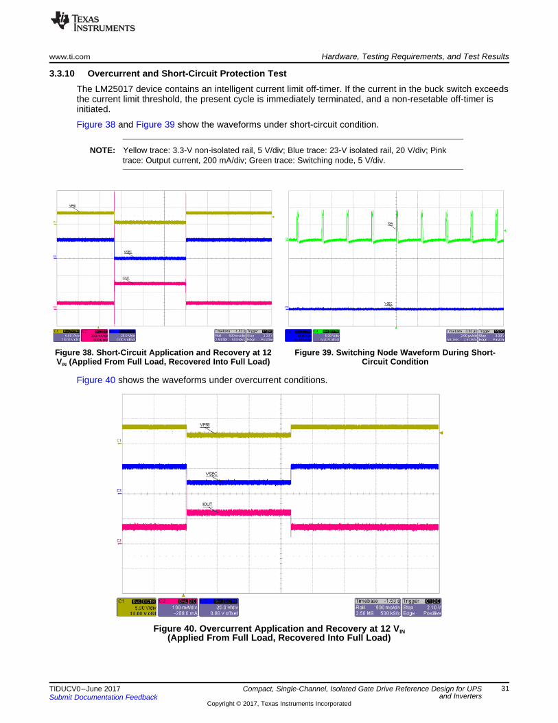
3.3.10 Overcurrent and Short-Circuit Protection TestThe LM25017 device contains an intelligent current limit off-timer. If the current in the buck switch exceedsthe current limit threshold, the present cycle is immediately terminated, and a non-resetable off-timer isinitiated.
Figure 38 and Figure 39 show the waveforms under short-circuit condition.
NOTE: Yellow trace: 3.3-V non-isolated rail, 5 V/div; Blue trace: 23-V isolated rail, 20 V/div; Pinktrace: Output current, 200 mA/div; Green trace: Switching node, 5 V/div.
Figure 38. Short-Circuit Application and Recovery at 12VIN (Applied From Full Load, Recovered Into Full Load)
Figure 39. Switching Node Waveform During Short-Circuit Condition
Figure 40 shows the waveforms under overcurrent conditions.
Figure 40. Overcurrent Application and Recovery at 12 VIN(Applied From Full Load, Recovered Into Full Load)

Hardware, Testing Requirements, and Test Results www.ti.com
32 TIDUCV0–June 2017Submit Documentation Feedback
Copyright © 2017, Texas Instruments Incorporated
Compact, Single-Channel, Isolated Gate Drive Reference Design for UPS andInverters
3.3.11 Performance Data
3.3.11.1 Efficiency and Regulation at 12-V InputTable 7 shows the efficiency and regulation performance data at a 12-V input.
Table 7. Efficiency and Regulation at 12-V Input
LOAD (%) IIN (mA) VOUT1 (V) VOUT2 (V) IOUT2 (mA) PIN (W) POUT (W) EFFICIENCY (%) REGULATIONVOUT1 (%)
REGULATIONVOUT2 (%)
0 18.452 3.3497 24.630 0.0268 0.2214 0.0007 0.3162 –0.5256 11.281810 29.356 3.3473 23.367 5.8950 0.3523 0.1377 39.0860 –0.5969 5.575420 43.659 3.3479 22.924 12.8330 0.5239 0.2942 56.1558 –0.5791 3.573930 61.349 3.3527 22.638 20.7700 0.7362 0.4702 63.8685 –0.4365 2.281740 78.984 3.3591 22.462 28.2500 0.9478 0.6346 66.9551 –0.2465 1.486550 92.365 3.3620 22.329 34.0530 1.1084 0.7604 68.6034 –0.1604 0.885660 107.967 3.3656 22.184 40.6520 1.2956 0.9018 69.6048 –0.0535 0.230470 121.610 3.3698 22.063 48.3580 1.4593 1.0669 73.1104 0.0713 –0.316380 136.610 3.3732 21.937 55.3210 1.6393 1.2136 74.0316 0.1722 –0.885690 152.960 3.3765 21.811 62.9180 1.8355 1.3723 74.7644 0.2702 –1.4548
100 169.360 3.3803 21.640 70.5300 2.0323 1.5263 75.1021 0.3831 –2.2274105 173.880 3.3816 21.580 72.6240 2.0866 1.5672 75.1078 0.4217 –2.4986140 240.750 3.4042 20.502 103.5120 2.8890 2.1222 73.4579 1.0928 –7.3691

www.ti.com Hardware, Testing Requirements, and Test Results
33TIDUCV0–June 2017Submit Documentation Feedback
Copyright © 2017, Texas Instruments Incorporated
Compact, Single-Channel, Isolated Gate Drive Reference Design for UPS andInverters
3.3.11.2 Efficiency and Regulation at 10-V InputTable 8 shows the efficiency and regulation performance data at a 10-V input.
Table 8. Efficiency and Regulation at 10-V Input
LOAD (%) IIN (mA) VOUT1 (V) VOUT2 (V) IOUT2 (mA) PIN (W) POUT (W) EFFICIENCY(%)
REGULATIONVOUT1 (%)
REGULATIONVOUT2 (%)
0 17.247 3.3433 24.221 0.02640 0.1725 0.0064 3.7075 –0.7382 10.660710 30.278 3.3424 23.171 5.8458 0.3028 0.1355 44.7365 –0.7649 5.863520 47.594 3.3448 22.781 12.7550 0.4759 0.2906 61.0522 –0.6936 4.081630 68.935 3.3511 22.506 20.6510 0.6894 0.4648 67.4217 –0.5066 2.825240 89.568 3.3568 22.309 28.0640 0.8957 0.6261 69.8999 –0.3374 1.925250 110.088 3.3617 22.089 35.3010 1.1009 0.7798 70.8310 –0.1919 0.920060 119.920 3.3659 22.028 40.8030 1.1992 0.8988 74.9507 –0.0672 0.641370 138.900 3.3701 21.866 47.9380 1.3890 1.0482 75.4652 0.0575 –0.098880 156.540 3.3742 21.702 54.7330 1.5654 1.1878 75.8794 0.1793 –0.848190 175.390 3.3790 21.483 61.9730 1.7175 1.3314 77.5159 0.3218 –1.8486
100 198.690 3.3865 21.118 71.0830 1.9869 1.5011 75.5514 0.5444 –3.5163130 274.750 3.4118 19.864 100.2750 2.7475 1.9919 72.4973 1.2956 –9.2455146 312.170 3.4234 19.205 114.1790 3.1217 2.1928 70.2440 1.6400 –12.2564

Hardware, Testing Requirements, and Test Results www.ti.com
34 TIDUCV0–June 2017Submit Documentation Feedback
Copyright © 2017, Texas Instruments Incorporated
Compact, Single-Channel, Isolated Gate Drive Reference Design for UPS andInverters
3.3.11.3 Efficiency and Regulation at 17-V InputTable 9 shows the efficiency and regulation performance data at a 17-V input.
Table 9. Efficiency and Regulation at 17-V Input
LOAD (%) IIN (mA) VOUT1 (V) VOUT2 (V) IOUT2 (mA) PIN (W) POUT (W) EFFICIENCY (%) REGULATIONVOUT1 (%)
REGULATIONVOUT2 (%)
0 21.926 3.3603 25.621 0.0278 0.3727 0.0007 0.1911 –0.2749 14.623810 29.744 3.3549 23.821 6.0091 0.5056 0.1431 28.3088 –0.4351 6.570920 39.968 3.3538 23.249 13.0150 0.6795 0.3026 44.5335 –0.4678 4.011930 52.804 3.3554 22.906 21.0150 0.8977 0.4814 53.6245 –0.4203 2.477440 65.182 3.3598 22.671 28.5130 1.1081 0.6464 58.3360 –0.2897 1.426050 75.137 3.3665 22.538 34.3700 1.2773 0.7746 60.6446 –0.0909 0.831060 87.247 3.3699 22.368 41.7520 1.4832 0.9339 62.9658 0.0100 0.070570 98.930 3.3726 22.242 48.7500 1.6818 1.0843 64.4721 0.0901 –0.493280 110.459 3.3751 22.132 55.8100 1.8778 1.2352 65.7783 0.1643 –0.985490 119.830 3.3775 22.036 63.5690 2.0371 1.4008 68.7644 0.2356 –1.4148
100 131.590 3.3797 21.925 71.4650 2.2370 1.5669 70.0424 0.3009 –1.9114107 134.890 3.3805 21.890 73.7200 2.2931 1.6137 70.3724 0.3246 –2.0680130 167.050 3.3581 21.021 92.4610 2.8399 1.9436 68.4410 –0.3402 –5.9558

Output Power (W)
Reg
ulat
ion
0.0 0.2 0.4 0.6 0.8 1.0 1.2 1.4 1.6-5%
-4%
-3%
-2%
-1%
0
1%
2%
3%
4%
5%
D002
VIN = 10 VVIN = 12 VVIN = 17 V
Output Power (W)
Effi
cien
cy
0.0 0.2 0.4 0.6 0.8 1.0 1.2 1.4 1.60
10%
20%
30%
40%
50%
60%
70%
80%
90%
D001
VIN = 10 VVIN = 12 VVIN = 17 V
www.ti.com Hardware, Testing Requirements, and Test Results
35TIDUCV0–June 2017Submit Documentation Feedback
Copyright © 2017, Texas Instruments Incorporated
Compact, Single-Channel, Isolated Gate Drive Reference Design for UPSand Inverters
3.3.12 Performance Curves
3.3.12.1 Efficiency With Output PowerFigure 41 shows the efficiency curve of the Fly-Buck converter with output power variation.
Figure 41. Efficiency versus Output Power
3.3.12.2 Regulation With Output PowerFigure 42 shows the regulation of the 3.3-V non-isolated output with output power variation.
Figure 42. Non-Isolated Output 3.3-V Regulation With Output Power
Output Power (W)
Reg
ulat
ion
0.0 0.2 0.4 0.6 0.8 1.0 1.2 1.4 1.6 1.8 2.0-20%
-10%
0
10%
20%
D003
VIN = 10 VVIN = 12 VVIN = 17 V
Hardware, Testing Requirements, and Test Results www.ti.com
36 TIDUCV0–June 2017Submit Documentation Feedback
Copyright © 2017, Texas Instruments Incorporated
Compact, Single-Channel, Isolated Gate Drive Reference Design for UPSand Inverters
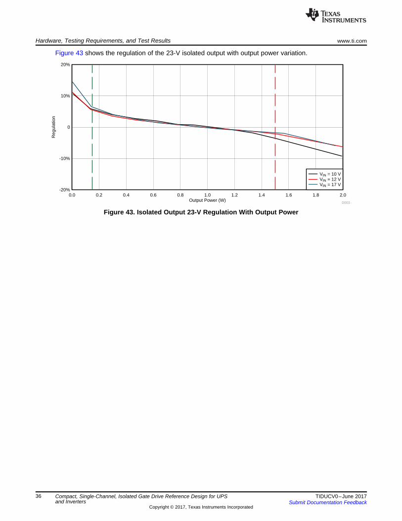
Figure 43 shows the regulation of the 23-V isolated output with output power variation.
Figure 43. Isolated Output 23-V Regulation With Output Power

www.ti.com Hardware, Testing Requirements, and Test Results
37TIDUCV0–June 2017Submit Documentation Feedback
Copyright © 2017, Texas Instruments Incorporated
Compact, Single-Channel, Isolated Gate Drive Reference Design for UPSand Inverters
3.3.13 Thermal MeasurementsFigure 44 and Figure 45 show the thermal measurements taken at ambient temperature (23.1°C) with a12-V input voltage, 56-nF load, and 20-kHz switching frequency after letting the board run for half an hour.
Figure 44. Thermal Measurements—Top View
Figure 45. Thermal Measurements—Bottom View

Hardware, Testing Requirements, and Test Results www.ti.com
38 TIDUCV0–June 2017Submit Documentation Feedback
Copyright © 2017, Texas Instruments Incorporated
Compact, Single-Channel, Isolated Gate Drive Reference Design for UPSand Inverters
Table 10. Highlighted Image Markers for Figure 44
NAME TEMPERATUREGate driver 63.6°CTransformer 44.7°C
Gate resistors 70.0°CZener diode 59.8°C
Snubber resistor 72.5°CBuck converter IC 42.8°C

www.ti.com Design Files
39TIDUCV0–June 2017Submit Documentation Feedback
Copyright © 2017, Texas Instruments Incorporated
Compact, Single-Channel, Isolated Gate Drive Reference Design for UPSand Inverters
4 Design Files
4.1 SchematicsTo download the schematics, see the design files at TIDA-01160.
4.2 Bill of MaterialsTo download the bill of materials (BOM), see the design files at TIDA-01160.
4.3 PCB Layout RecommendationsNote that the design contains high voltages. The layout must be done with extreme care.
4.3.1 Fly-Buck Converter Stage Specific Guidelines• The loop consisting of the input capacitor (C3), VIN pin, and GND pin carries switching currents.
Therefore, the input capacitor should be placed close to the IC, directly across VIN and GND pins, andthe connections to these two pins should be direct to minimize the loop area.
• Provide sufficient vias for the input capacitor and output capacitor.• The SW node switches rapidly between VIN and GND every cycle and is therefore a possible source
of noise. Minimize the SW node area. Keep the SW trace as physically short and wide as practical tominimize radiated emissions.
• Place the voltage feedback loop away from the high-voltage switching trace, and preferably have aground shield.
• The trace of the VFB node should be as small as possible to avoid noise coupling.• Place the bootstrap capacitor as close to the IC as possible, and minimize the connecting trace length
and loop area.
4.3.2 Gate Driver Specific Guidelines• Connect the low-ESR and low-ESL capacitors close to the UCC5320S between the VCC1 and GND1
pins and between the VCC2 and VEE2 pins to support high peak currents when turning on the externalpower transistor.
• A PCB cutout is recommended to ensure good isolation performance between the primary andsecondary side of the UCC5320S. To do this, avoid placing any PCB traces or copper below thedevice.
• Confine the high peak currents that charge and discharge the transistor gates to a minimal physicalarea as this will decrease the loop inductance and minimize noise on the gate terminals of thetransistors. To ensure this, connect the TIDA-01160 board with very short leads to the transistors.
A proper PCB layout can help dissipate heat from the devices to the PCB and minimize junction to boardthermal impedance. See the placement and routing guidelines and layout example in the LM25017 andUCC5320 datasheets.
4.3.3 Layout PrintsTo download the layer plots, see the design files at TIDA-01160.
4.4 Altium ProjectTo download the Altium project files, see the design files at TIDA-01160.
4.5 Gerber FilesTo download the Gerber files, see the design files at TIDA-01160.

Design Files www.ti.com
40 TIDUCV0–June 2017Submit Documentation Feedback
Copyright © 2017, Texas Instruments Incorporated
Compact, Single-Channel, Isolated Gate Drive Reference Design for UPSand Inverters
4.6 Assembly DrawingsTo download the assembly drawings, see the design files at TIDA-01160.
5 Related Documentation
1. Texas Instruments, AN-2292 Designing an Isolated Buck (Fly-Buck) Converter, Application Report(SNVA674)
2. Texas Instruments, Pick the right turns ratio for a Fly-Buck converter, Editorial Reprint (SLPY004)3. Xiang Fang, Wei Liu, and Anoop Chadaga, Product How-to: Fly-Buck adds well-regulated isolated
outputs to a buck without optocouplers, EDN Network (http://www.edn.com/design/power-management/4429791/2/Product-How-to--Fly-Buck-adds-well-regulated-isolated-outputs-to-a-buck-without-optocouplers-)
4. Robert Kollman, Power Tip 34: Design a simple, isolated bias supply, EE Times(http://www.eetimes.com/author.asp?doc_id=1278680)
5. Texas Instruments, Design a Flybuck Solution With Optocoupler to Improve Regulation Performance,Application Report (SNVA727)
6. Texas Instruments, Transient Response versus Ripple – An Analysis of Ripple Injection TechniquesUsed in Hysteretic Controllers, Application Report (SLVA653)
5.1 TrademarksFly-Buck, C2000, Piccolo, LaunchPad are trademarks of Texas Instruments.All other trademarks are the property of their respective owners.
6 About the AuthorsSALIL CHELLAPPAN is a system manager, member, and group technical staff at Texas Instruments,where he is responsible for developing customized power solutions as part of the power delivery, industrialsegment. Salil brings to this role his extensive experience in power electronics, power conversion,EMI/EMC, power and signal integrity, and analog circuits design spanning many high-profile organizations.Salil holds a bachelor of technology degree from the University of Kerala.
LATIF AMEER BABU is the End Equipment Lead for UPS-Power Delivery Sector. He is responsible forbusiness development, marketing and architecting TI reference designs for UPS. Latif brings to this rolehis extensive experience in power electronics, high-frequency DC-DC converter, and analog circuit design.Latif earned his master of technology in power electronics and power systems from Indian Institute ofTechnology, Mumbai.Latif is a member of the Institute of Electrical and Electronics Engineers (IEEE) andhas one US patent.
YAMINI SHARMA is a systems engineer at Texas Instruments, where she is responsible for developingreference design solutions for the power delivery, industrial segment. Yamini earned her bachelor oftechnology degree in electronics and communication from Delhi Technological University (formerly DCE),Delhi.

IMPORTANT NOTICE FOR TI DESIGN INFORMATION AND RESOURCES
Texas Instruments Incorporated (‘TI”) technical, application or other design advice, services or information, including, but not limited to,reference designs and materials relating to evaluation modules, (collectively, “TI Resources”) are intended to assist designers who aredeveloping applications that incorporate TI products; by downloading, accessing or using any particular TI Resource in any way, you(individually or, if you are acting on behalf of a company, your company) agree to use it solely for this purpose and subject to the terms ofthis Notice.TI’s provision of TI Resources does not expand or otherwise alter TI’s applicable published warranties or warranty disclaimers for TIproducts, and no additional obligations or liabilities arise from TI providing such TI Resources. TI reserves the right to make corrections,enhancements, improvements and other changes to its TI Resources.You understand and agree that you remain responsible for using your independent analysis, evaluation and judgment in designing yourapplications and that you have full and exclusive responsibility to assure the safety of your applications and compliance of your applications(and of all TI products used in or for your applications) with all applicable regulations, laws and other applicable requirements. Yourepresent that, with respect to your applications, you have all the necessary expertise to create and implement safeguards that (1)anticipate dangerous consequences of failures, (2) monitor failures and their consequences, and (3) lessen the likelihood of failures thatmight cause harm and take appropriate actions. You agree that prior to using or distributing any applications that include TI products, youwill thoroughly test such applications and the functionality of such TI products as used in such applications. TI has not conducted anytesting other than that specifically described in the published documentation for a particular TI Resource.You are authorized to use, copy and modify any individual TI Resource only in connection with the development of applications that includethe TI product(s) identified in such TI Resource. NO OTHER LICENSE, EXPRESS OR IMPLIED, BY ESTOPPEL OR OTHERWISE TOANY OTHER TI INTELLECTUAL PROPERTY RIGHT, AND NO LICENSE TO ANY TECHNOLOGY OR INTELLECTUAL PROPERTYRIGHT OF TI OR ANY THIRD PARTY IS GRANTED HEREIN, including but not limited to any patent right, copyright, mask work right, orother intellectual property right relating to any combination, machine, or process in which TI products or services are used. Informationregarding or referencing third-party products or services does not constitute a license to use such products or services, or a warranty orendorsement thereof. Use of TI Resources may require a license from a third party under the patents or other intellectual property of thethird party, or a license from TI under the patents or other intellectual property of TI.TI RESOURCES ARE PROVIDED “AS IS” AND WITH ALL FAULTS. TI DISCLAIMS ALL OTHER WARRANTIES ORREPRESENTATIONS, EXPRESS OR IMPLIED, REGARDING TI RESOURCES OR USE THEREOF, INCLUDING BUT NOT LIMITED TOACCURACY OR COMPLETENESS, TITLE, ANY EPIDEMIC FAILURE WARRANTY AND ANY IMPLIED WARRANTIES OFMERCHANTABILITY, FITNESS FOR A PARTICULAR PURPOSE, AND NON-INFRINGEMENT OF ANY THIRD PARTY INTELLECTUALPROPERTY RIGHTS.TI SHALL NOT BE LIABLE FOR AND SHALL NOT DEFEND OR INDEMNIFY YOU AGAINST ANY CLAIM, INCLUDING BUT NOTLIMITED TO ANY INFRINGEMENT CLAIM THAT RELATES TO OR IS BASED ON ANY COMBINATION OF PRODUCTS EVEN IFDESCRIBED IN TI RESOURCES OR OTHERWISE. IN NO EVENT SHALL TI BE LIABLE FOR ANY ACTUAL, DIRECT, SPECIAL,COLLATERAL, INDIRECT, PUNITIVE, INCIDENTAL, CONSEQUENTIAL OR EXEMPLARY DAMAGES IN CONNECTION WITH ORARISING OUT OF TI RESOURCES OR USE THEREOF, AND REGARDLESS OF WHETHER TI HAS BEEN ADVISED OF THEPOSSIBILITY OF SUCH DAMAGES.You agree to fully indemnify TI and its representatives against any damages, costs, losses, and/or liabilities arising out of your non-compliance with the terms and provisions of this Notice.This Notice applies to TI Resources. Additional terms apply to the use and purchase of certain types of materials, TI products and services.These include; without limitation, TI’s standard terms for semiconductor products http://www.ti.com/sc/docs/stdterms.htm), evaluationmodules, and samples (http://www.ti.com/sc/docs/sampterms.htm).
Mailing Address: Texas Instruments, Post Office Box 655303, Dallas, Texas 75265Copyright © 2017, Texas Instruments Incorporated


![Simulating the Source of Polarization Charge in AlGaN/GaN ... · the gate reverse biased region, though it is stated in ref.[2] that drain current corresponded with gate cur-rent](https://img.pdfslide.us/doc/110x75/5e29e34439c4710fb36c9722/simulating-the-source-of-polarization-charge-in-algangan-the-gate-reverse-biased.jpg)