Embed Size (px)
Citation preview
Boise State UniversityScholarWorksElectrical and Computer Engineering FacultyPublications and Presentations
Department of Electrical and ComputerEngineering
9-15-2009
Compact Optical Curvature Sensor with a FlexibleMicrodisk Laser on a Polymer SubstrateWan KuangBoise State University
M. H. ShihNational Chiao-Tung University, Taiwan
K. S. HsuNational Chiao-Tung University, Taiwan
Y. C. YangAcademia Sinica, Taiwan
Y. C. WangNational Tsing-Hua University, Taiwan
See next page for additional authors
This is an author-produced, peer-reviewed version of this article. The final, definitive version of this document can be found online at Optics Letters,published by Optical Society of America. Copyright restrictions may apply. DOI: 10.1364/OL.34.002733

AuthorsWan Kuang, M. H. Shih, K. S. Hsu, Y. C. Yang, Y. C. Wang, S. K. Tsai, Y. C. Liu, Z. C. Chang, and M. C. Wu
This article is available at ScholarWorks: https://scholarworks.boisestate.edu/electrical_facpubs/52
1
Compact Optical Curvature Sensor with a Flexible
Microdisk Laser on a Polymer Substrate
M. H. Shih1,2, *, K. S. Hsu2, Wan Kuang3, Y. C. Yang1, Y. C. Wang4, S. K. Tsai4,
Y. C. Liu4, Z. C. Chang4 and M. C. Wu4
1 Research Center for Applied Sciences (RCAS), Academia Sinica, Taiwan
2 Department of Photonics, National Chiao-Tung University, Taiwan
3 Department of Electrical & Computer Engineering, Boise State University, 1910 University
Drive, Boise, ID 83725, USA
4 Department of Electrical Engineering, National Tsing-Hua University, Taiwan.
*Corresponding author: [email protected]
In this paper, a chip-scale compact optical curvature sensor was demonstrated. It consists
of a low threshold InGaAsP microdisk laser on a flexible polydimethylsiloxane polymer
substrate. The curvature dependence of lasing wavelength was characterized by bending
the cavity at different bending radii. The measurements showed that the lasing wavelength
decreases monotonously with an increasing bending curvature. A good agreement between
experiment and three-dimensional finite-difference time-domain simulation was also
obtained. The sensitivity of the compact device to the bending curvature is -23.7 nm/mm
form the experiment.
OCIS codes: 140.5960, 140.3948, 250.2080, 280.4788
2
Introduction
In recent years, semiconductor microdisk cavities have attracted a lot of attention for applications
in photonic integrated circuits due to their promising and versatile optical functions, for instance,
lasers [1-5], modulators [6-8] and sensors [9-12]. In addition, the optical curvature sensor had
been studied widely with the long period fiber grating system [13-17]. This optical fiber
technology can be applied in the curvature monitoring for larger structures such as bridges and
buildings. However, these fiber gratings are not suitable for curvature sensing in either chip-scale
integrated circuits or two-dimensional in-plane detection due to its structure size and special
geometry. In this study, we demonstrated a compact optical curvature sensor with the InGaAsP
microdisk laser on a polydimethylsiloxane (PDMS) substrate. The dimension of the sensor is less
than 10 microns. This small size makes it suitable not only for monitoring the local curvature
within few μm region, but also for performing the curvature detection or mapping in two-
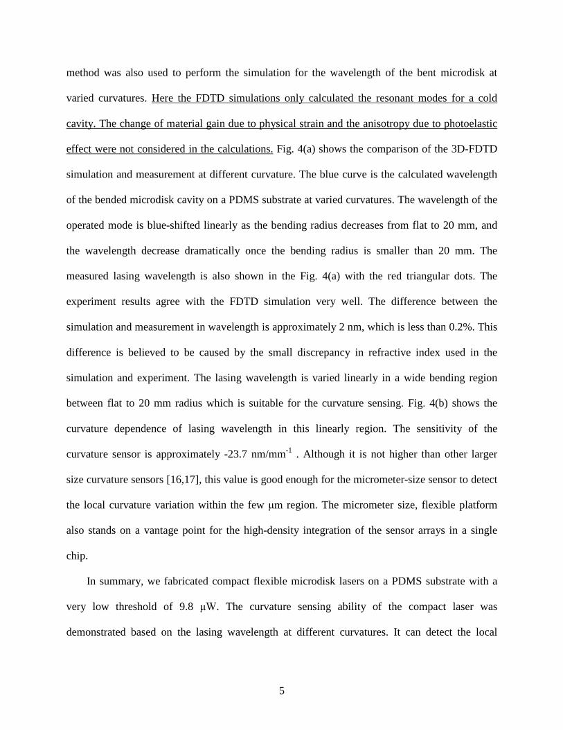
dimensional planes with the microdisk sensor array. Fig. 1 shows the illustration of an InGaAsP
microdisk cavity on a PDMS substrate. The InGaAsP microdisk is embedded inside a flexible
PDMS layer which is benefit to the bending ability of the cavity. The low index (n=1.41) of the
PDMS also improve the vertical confinement of the optical mode in the disk, compare to
microdisks on Si or GaAs substrates. With a flexible platform, this novel laser can function not
only as a light source for the photonic integrated circuits on the non-flat surface, but also as a
compact sensing device for the curvature of the bent substrate.
The microdisk cavities were implemented in a 240nm thick InGaAsP layer on the InP
substrate. The InGaAsP layer consists of four 10nm thick strained InGaAsP quantum wells
(QWs) which is designed for the lasers operated near 1550nm wavelength. A silicon nitride
(SiNx) layer and a polymethylmethacrylate (PMMA) layer are deposited subsequently for the
3
dry etching processes and electron beam lithography. The microdisk patterns were defined by
electron beam lithography followed by two dry etching steps with CHF3/O2 mixture and
CH4/Cl2/H2 mixture gas in the inductive couple plasma (ICP) system. The microdisk structures
then flipped and mounted to an 80 μm thick PDMS substrate. The InP substrate was removed by
HCl solution. The size of the fabricated microdisk array is from 0.5 to 10μm in diameter for
studying the compact lasers. Fig. 1(c) shows the SEM images of a microdisk array with varied
diameters on the PDMS substrate. Fig. 1(d) is a close-up view of a microdisk cavity with a
diameter of 4.75 μm. The adhesion between the InGaAsP microdisk and the PDMS substrate is
shown to be reliable for bending up to 10 mm radius.
The microdisk lasers were optically pumped at room temperature by an 850 nm
wavelength diode laser at normal incidence with a 1.5% duty cycle and a 30 ns pulse width. The
pump beam was focused on the devices by a 100x objective lens. The pump beam spot size is
approximately 2 μm in diameter. The output power was collected by a multi-mode fiber
connected to an optical spectrum analyzer. The lasing action of the microdisk cavities was
achieved with a low threshold. Fig. 2(a) shows a lasing spectrum from a microdisk laser with
4.75 μm diameter. The lasing wavelength is around 1571.9 nm. The light-in-light-out (L-L)
curve of this laser is shown in the Fig. 2(b). The threshold of the laser happened at 0.18 mW of
incident pumped power. We roughly estimated the absorbed power in 240nm InGaAsP layer by
considering the material absorption (~2 μm-1) and surface reflectivity (~0.29). From the
estimated values, only 5.4% of incident power is absorbed by the QWs. Therefore the effective
threshold power is approximately 9.8 μW. This low threshold power of a single laser will benefit
the further integration of the laser array. In order to understand the cavity mode of the flexible
microdisk cavity, three-dimensional (3-D) finite-difference time-domain (FDTD) method was
4
used to perform the simulation with a domain of up to 10 μm x 10 μm x 5 μm and 4 nm grid
size for all three dimensions.
After the characterizing the microdisk lasers on a flat surface, the cavity was bended
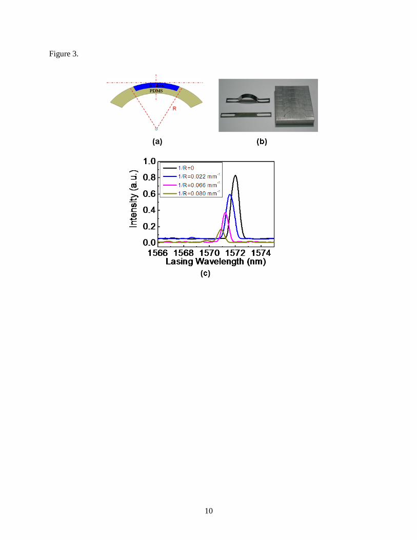
along the diameter of the disk on a bent metal surface. Fig. 3(a) illustrates the the microdisk
cavity with the curvature 1/R after bending. We expected the lasing characteristics of the
microdisk can be manipulated by varying the bending radius R. The microdisk was mounted on
the metal plates with different bending radius. These curved metal surfaces were formed by
bending the metal plates in the slots with varied bending radii with a homemade curvature
component. Fig. 3(b) shows the curvature component and the curved metal plates. We also verify
the surface curvature of the device with optical microscope and SEM images after the device is
mounted on the bent metal surface. In the experiment, the variation of lasing wavelength was
observed by bending the microdisk cavity and fixing the pumped conditions and power. Fig. 3(c)
shows the lasing spectra of a 4.75 μm microdisk laser at the varied bending curvatures
The lasing mode from the measured microdisk was verified to be
the first-order mode by comparing the measured and simulated spectra. The calculated Hz
components of the first-order mode of a 4.75 μm microdisk cavity at the flat surface is shown in
Fig. 2(c).
(1/R = 0,
0.022, 0.066 and 0.080 mm-1) under the same pumping conditions and fixed 2.0 mW incident
pumped power. The microdisk achieved lasing at all these bending curvatures. According to the
data, the lasing wavelength reduces as the bending curvature increases. This special blue shifted
characteristic can be applied to compensate the red shift of lasing wavelength due to the
operating temperature increase, especially for the compact lasers and laser arrays. The
InGaAsP/PDMS hybrid microdisk cavity is shown to be reliable for bending up to 10 mm radius,
according to the SEM images and lasing data after several bending processes. The 3-D FDTD
5
method was also used to perform the simulation for the wavelength of the bent microdisk at
varied curvatures. Here the FDTD simulations only calculated the resonant modes for a cold
cavity. The change of material gain due to physical strain and the anisotropy due to photoelastic
effect were not considered in the calculations.
In summary, we fabricated compact flexible microdisk lasers on a PDMS substrate with a
very low threshold of 9.8 μW. The curvature sensing ability of the compact laser was
demonstrated based on the lasing wavelength at different curvatures. It can detect the local
Fig. 4(a) shows the comparison of the 3D-FDTD
simulation and measurement at different curvature. The blue curve is the calculated wavelength
of the bended microdisk cavity on a PDMS substrate at varied curvatures. The wavelength of the
operated mode is blue-shifted linearly as the bending radius decreases from flat to 20 mm, and
the wavelength decrease dramatically once the bending radius is smaller than 20 mm. The
measured lasing wavelength is also shown in the Fig. 4(a) with the red triangular dots. The
experiment results agree with the FDTD simulation very well. The difference between the
simulation and measurement in wavelength is approximately 2 nm, which is less than 0.2%. This
difference is believed to be caused by the small discrepancy in refractive index used in the
simulation and experiment. The lasing wavelength is varied linearly in a wide bending region
between flat to 20 mm radius which is suitable for the curvature sensing. Fig. 4(b) shows the
curvature dependence of lasing wavelength in this linearly region. The sensitivity of the
curvature sensor is approximately -23.7 nm/mm-1 . Although it is not higher than other larger
size curvature sensors [16,17], this value is good enough for the micrometer-size sensor to detect
the local curvature variation within the few μm region. The micrometer size, flexible platform
also stands on a vantage point for the high-density integration of the sensor arrays in a single
chip.

6
curvature variation due to the compact size of the microdisk. The compact flexible microdisk
laser and its very low threshold power promise the chip-scale integration of the high density
sensor array for future applications.
7
Figure captions
Fig. 1
The illustrations of an InGaAsP microdisk cavity on a polydimethylsiloxane (PDMS) polymer
substrate from (a) angle-view and (b) cross section-view. (c) A SEM image of a microdisk lasers
array on a PDMS substrate. (d) A magnified SEM image of a 4.75μm microdisk laser on a
PDMS substrate.
Fig. 2
(a)The lasing spectrum and (b) light-in-light-out (LL) curve of a 4.75μm microdisk laser on a
PDMS substrate. The lasing wavelength is 1571.9 nm, and the incident threshold power is 0.18
mW. (c)The calculated Hz mode profile for a 4.75μm microdisk laser on a PDMS substrate form
3-D FDTD simulation.
Fig. 3
(a)The illustration of a bent microdisk cavity on a PDMS substrate with a bending radius of R.
(b) The home-made curvature component (right) and the bendable metal plates (left) for
characterization. (c) The measured lasing spectra from a microdisk laser on a PDMS substrate at
varied curvatures under the fixed pumped conditions and 2 mW incident pumped power.
Fig. 4
(a) The comparison of the FDTD simulated and measured lasing wavelength at varied bending
radii. (b) The measured lasing wavelength versus the device curvature within the linear sensing
region. The sensitivity is approximately -23.7 nm/mm-1.
8
Figure 1.
9
Figure 2.
10
Figure 3.
11
Figure 4.
0 20 40 60 801555
1560
1565
1570
1575 (a)
Lasin
g W
avel
engt
h (n
m)
Surface Radius (mm)
Simulation Measurement
0.01 0.02 0.03 0.04 0.051570
1571
1572
1573
Wav
elen
gth
(nm
)
Curvature 1/R (mm-1)
Sensitivity ~ 23.7 nm/mm-1
(b)
12
References
1. S. L. McCall, A. F. J. Levi, R. E. Slusher, S. J. Pearton, and R. A. Logan, “Whispering-
gallery mode microdisk lasers,” Appl. Phys. Lett. 60, 289-291 (1992)
2. Masayuki Fujita, Atsushi Sakai, and Toshihiko Baba, “Ultrasmall and Ultralow Threshold
GaInAsP–InP Microdisk Injection Lasers: Design, Fabrication, Lasing Characteristics, and
Spontaneous Emission Factor,” IEEE J. Selected Topics in Quantum Electronics 5, 673-681
(1999).
3. Seung June Choi, Kostadin Djordjev, Sang Jun Choi, and P. Daniel Dapkus, ”Microdisk
Lasers Vertically Coupled to Output Waveguides,” IEEE Photon. Technol. Lett. 15, 1330-
1332 (2003)
4. D. S. Song, J. K. Hwang, C. K. Kim, I. Y. Han, D. H. Tang, and Y. H. Lee, “InGaAsP
Microdisk Lasers on AlxOy,” IEEE Photon. Technol. Lett. 12, 954-956 (2000)
5. A. C. Tamboli, E. D. Haberer, R. Sharma, K. H. Lee, S. Nakamura, and E. L. Hu, “Room-
temperature continuous-wave lasing in GaN/InGaN microdisks,” Nat. Photonics 1, 61-64
(2007)
6. Kostadin Djordjev, Sang-Jun Choi, Seung-June Choi, and P. D. Dapkus,“Active
Semiconductor Microdisk Devices,” J. Lightwave Technol. 20, 105-113 (2002)
7. Linjie Zhou and Andrew W. Poon, “Silicon electro-optic modulators using p-i-n diodes
embedded 10-micron-diameter microdisk resonators,” Opt. Express 14, 6851-6857 (2006)
8. Q.F. Xu, B. Schmidt, S. Pradhan, and M. Lipson, “Micrometre-scale silicon electro-optic
modulator,” Nature (London) 435, 325-327 (2005).
9. Sang-Yeon Cho and Nan Marie Jokerst,” A Polymer Microdisk Photonic Sensor Integrated
Onto Silicon,” IEEE Photonic Technol. Lett. 18, 2096-2098 (2006)
13
10. Jun Yang and L. Jay Guo, “Optical Sensors Based on Active Microcavities,” IEEE J.
Selected Topics in Quantum Electronics 12, 143-147 (2006)
11. Juejun Hu, Nathan Carlie, Ning-Ning Feng, Laeticia Petit, Anu Agarwal, Kathleen
Richardson, and Lionel Kimerling, “Planar waveguide-coupled high-index-contrast high-Q
resonators in chalcogenide glass for sensing,” Optics Lett. 33, 2500-2502 (2008)
12. Bipin Bhola, Hyun-Chae Song, Hidehisa Tazawa, and William H. Steier, “Polymer
Microresonator Strain Sensors,” IEEE Photonic Technol. Lett. 17, 867-869 (2005)
13. Stephen W James and Ralph P Tatam, “Optical fibre long-period grating sensors:
characteristics and application,” Meas. Sci. Technol. 14, R49–R61 (2003)
14. H.J. Patrick, C.C. Chang and S.T. Vohra, “Long period fibre gratings for structural bend
sensing,” Electronics Lett. 34, 1773-1775 (1998)
15. Yun-Jiang Rao, Yi-Ping Wang, Zeng-Ling Ran, and Tao Zhu,” Novel Fiber-Optic Sensors
Based on Long-Period Fiber Gratings Written by High-Frequency CO2 Laser Pulses,” J.
Lightw. Technol. 21, 1320-1327 (2003)
16. Y. Liu, L. Zhang, J. A. R. Williams, and I. Bennion, ”Optical Bend Sensor Based on
Measurement of Resonance Mode Splitting of Long-Period Fiber Grating,” IEEE Photonic
Technol. Lett. 12, 531-533 (2000)
17. Fufei Pang, Wenbin Liang, Wenchao Xiang, Na Chen, Xianglong Zeng, Zhenyi Chen, and
Tingyun Wang, “Temperature-Insensitivity Bending Sensor Based on Cladding-Mode
Resonance of Special Optical Fiber,” IEEE Photonic Technol. Lett. 21, 76-78 (2009)