Embed Size (px)
Citation preview
INTRUMENTATION Revista Mexicana de Fısica59 (2013) 560–569 NOVEMBER-DECEMBER 2013
Common-source cold-FET used to validate noise figure measurementsand on-wafer FET noise parameters
B. E. Figueroa Resendiz, M. C. Maya Sanchez, and J. A. Reynoso HernandezCentro de Investigacion Cientıfica y de Educacion Superior de Ensenada,
Division de Fısica Aplicada, Departamento de Electronica y Telecomunicaciones,Carretera Ensenada-Tijuana No. 3918, Zona Playitas, 22860, Ensenada, B.C. Mexico.
e-mail: [email protected]; [email protected]; [email protected]
Received 1 October 2012; accepted 25 July 2013
This work proposes the use of a common-source cold-FET with gate forward biased to validate the noise figure measurements and the noiseparameters of on-wafer transistors. Since a common-source cold-FET behaves as an attenuator, its noise figure and noise parameters canbe determined from S-parameters measurements. Three methods for determining the noise parameters of the common-source cold-FETare investigated. The first one uses the noise correlation matrix for passive devices (the S-parameters), the second one is the tuner methodand the third one is the F50 method. The noise figure measured and the noise figure computed from S-parameters agree quite well. Thenoise parameters extracted with the tuner method and the F50 method show good correlation with the noise parameters computed with theS-parameters. These results validate both the noise figure measurements and the noise parameters extraction.
Keywords: Noise figure; noise parameters; cold-FET; source-pull tuner method; F50 method.
PACS: 85.30.De; 06.20.fb; 84.40.Dc
1. Introduction
Noise figure is one of the receiver parameters; that indicatesits ability to process low-level signals. This figure of merit ismainly dictated by the low noise amplifier (LNA), and it de-pends on the transistors’ noise parameters [1,2]. The knowl-edge of noise figure at different input impedances allows thedetermination of the four noise parameters (NPs) [3]: min-imum noise figure, Fmin, noise resistance Rn, and the mag-nitude and phase of the optimum reflection coefficient,Γopt
(or the real and the imaginary parts of optimum admittance,Yopt=Gopt+jBopt). The NPs depend on both the frequency andthe bias point.
The transistor NPs can be determined by using either themultiple-impedance technique (tuner method) [4-8] or theF50 method [9,10]. The tuner method uses measures of noisefigure at different impedances presented at the input of thedevice under test (DUT). This technique can be applied toany two-port device. The F50 method requires the knowledgeof the transistor noise model, and only needs measurementsof the transistor noise figure when its input is loaded witha broadband load near 50 ohms. To minimize errors in thenoise parameters extraction the F50 method uses frequencyredundancy. Therefore, errors in the measurements of noisefigure and reflection coefficient preclude the correct determi-nation of the NPs. Therefore, high reliable measurements ofnoise figure and reflection coefficients are required. In thissense, noise verification standards are also sought after in or-der to validate the noise figure measurements of mismatcheddevices.
The common-gate cold-FET configuration has been pro-posed as a verification standard to check the accuracy ofNPs [11-12]. The cold-FET in common-gate configuration
can be used as a noise verification standard since its noisefigure and noise parameters can be directly computed fromthe device S-parameters. The common-gate cold-FET tran-sistor behaves as a variable attenuator in function of the biaspoint, and their noise parameters are the same order of mag-nitude as the active device ones. Besides, the common-gatecold-FET transistor can also be used to check the accuracyof the noise figure setup [11]. However, the common-gatecold-FET configuration is not a common on-wafer FET con-figuration and its implementation requires additional techno-logical steps. For example, a specific bonding to become thetransistor in common-gate configuration or a specific foundrydesign, are needed. For on-wafer transistors, the common-source is the most common configuration, and therefore theimplementation of the common-source cold-FET configura-tion is straightforward. Even though the common-sourcecold-FET exhibits a large noise figure (around 10 dB) [11], itcan be used as noise verification standard, but not to check theaccuracy of the noise figure setup (especially, when noise fig-ure values less than 2 dB have to be measured). For these rea-sons, in this work a common-source cold-FET with gate for-ward biased is proposed to validate the noise figure measure-ments and the noise parameters of on-wafer transistors only.Like the common-gate cold-FET, the common-source cold-FET exhibits mismatches close to an active device, there-fore the noise figure measurements are performed in a simi-lar condition. Furthermore, the performance of both the tunermethod and the F50 method for determining the noise param-eters in the frequency range of 5-10 GHz are validated usingthe common-source cold-FET as verification standard.
It is important to comment that the common-source cold-FET configuration under reverse bias has been used as noisesource [13-14]; but not as calibration element due to large
COMMON-SOURCE COLD-FET USED TO VALIDATE NOISE FIGURE MEASUREMENTS AND ON-WAFER FET NOISE PARAMETERS561
noise level. By contrast, the common-source cold-FET underthe forward bias behaves as attenuator it can be used to verifynoise figure measurements.
2. Noise figure and noise parameters of thecommon-source cold-FET
A common-source cold-FET configuration is proposed tovalidate the measured noise figure and the noise parametersextracted by the F50 and tuner methods. The common-sourcecold-FET is implemented by using a common-source MES-FET biased with VGS >Vbi >0 (Vbi is the “built-in voltage”)and floating VDS (open drain). The procedure to obtain thenoise parameters is described next.
2.1. Computation of the passive device noise parametersusing S-parameters
Since the common-source cold-FET is a passive element, itsnoise figure is given by [15]:
F = L, (1)
where L are the device losses computed from the S-parameters. The available gain isG = 1/L.
On the other hand, the common-source cold-FET’s noiseparameters can also be computed from the S-parametersthrough the correlation matrices, as described as follows. Forpassive devices, the correlation matrix, in its chain represen-tationCAT , is determined from [16,17] as
CAT = 2kTa∆fPZA
ZD + ZD†
PZA† , (2)
Where k denotes the Boltzmann’s constant(1.3807×10⁻²³ JK−1), T0 is the standard temperature(290 K) and∆f is the incremental noise bandwidth. Thesuperscript ‘†’ denotes the conjugate transpose,Ta is theroom temperature (300 K),ZD is the device impedance ma-trix computed from its S-parameter measurements. Finally,PZA is the transformation matrix from impedance to chainrepresentation [17], given by
PZA =
1 ZD
11ZD
21
0 1ZD
21
. (3)
The noise parameters can be derived fromCAT [12,17],since
CAT =
[CAT
11 CAT12
CAT21 CAT
22
]= 4kT0∆f
Rn12 (Fmin−1)−RnY ∗
opt
12 (Fmin−1)−RnYopt Rn |Yopt|2
. (4)
Then, from Eq. (4), the noise parameters are given as
Rn =CAT
11
4kT0∆f, (5)
Gopt =
√√√√CAT22
CAT11
−(
Im(CAT
12
)
CAT11
)2
, (6)
Bopt =Im
(CAT
12
)
CAT11
, (7)
and
Fmin = 1 +1
2kT0∆f
[CAT
12 + CAT11 Y ∗
opt
]. (8)
The asterisk denotes the complex conjugate.
2.2. Determination of the noise parameters using theF50 technique
In the F50 technique the noise parameters are determinedfrom the knowledge of the device noise model and from themeasurements of its noise figure, at different frequencies,when a source admittance is connected to the input of theDUT [9-10]. The analysis of the noise equivalent circuit al-lows us to determine the correlation matrix,CAT [10,16],
which models the whole noise transistor behavior. Then,from the knowledge ofCAT the noise parameters are com-puted according to the procedure described next. It is im-portant to comment that, to the author’s knowledge, noiseanalysis of the common-source cold-FET applying the F50
technique has not been reported yet.
The active region of the transistor, biased as a cold-FET,is modeled as a Schottky diode in series with a channelresistance, whose impedance is denoted asZ int, shown inFig. 1(a). The small-signal equivalent circuit of the common-source cold-FET is shown in Fig. 1(b) [18], where the noisesources are also included. The parasitic elements (Rg, Rd,Rs, Lg, Ld, Ls) are bias independent, while the active regionmodeled byZ int is bias dependent. The parasitic elements ofthe equivalent circuit are extracted according to the methoddescribed by Reynosoet al. [18]. Once the parasitic elementsare known, thenZ int is de-embedded.
The noise sources of the intrinsic transistor are repre-sented as noise source voltages egs and eds, where the for-mer is associated to the gate-source terminal and the later isassociated to the drain-source terminal. The intrinsic noisesources egs and eds are arranged into the correlation matrix
Rev. Mex. Fis.59 (2013) 560–569
562 B. E. FIGUEROA RESENDIZ, M. C. MAYA SANCHEZ, AND J. A. REYNOSO HERNANDEZ
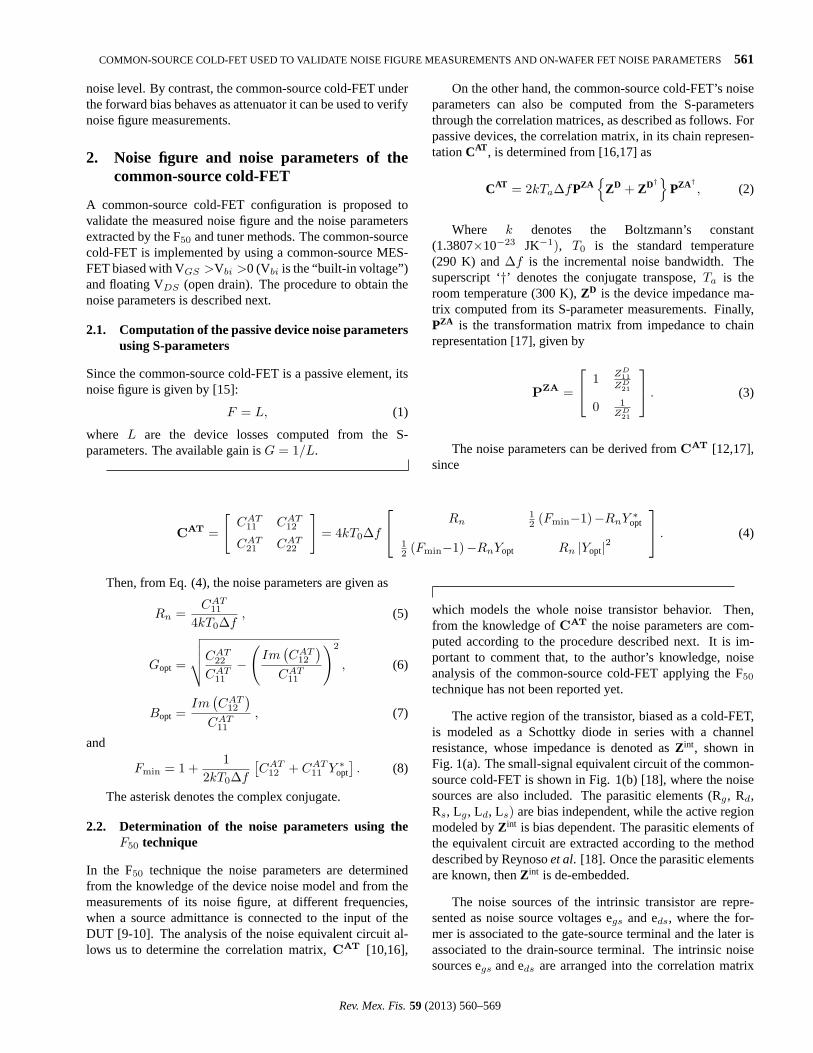
FIGURE 1. Common-source cold-FET: (a) Equivalent circuit forthe intrinsic transistor. Note:αg andα are the factors related to thegate-source current distribution, and to the gate-drain current dis-tribution, respectively. At low current values,αg =1/3 andα =1/2.Rch is the channel resistance, n is the ideality factor and q is theelectron charge. (b) Total electrical equivalent circuit, divided innetworks and including noise sources.
denoted asCZint. The noise contribution of the parasitic ele-ments is modeled by means of the noise source voltages eRg,eRd and eRs, associated to the gate, the drain and the sourceparasitic resistances, respectively.
To obtain the total correlation matrix, the equivalent cir-cuit is divided into four networks, as shows in Fig. 1(b).
To model the noise contribution of the intrinsic transistor,the impedance matrix representationCZint is given by:
CZint =
e2gs egse∗ds
egse∗gs e2ds
=
[C int
11 C int12
C int21 C int
22
]. (9)
Next, the correlation matrix associated to the source network,CZS, is added toCZint:
CZiS= CZint+CZS, (10)
where CZS = 2kT0∆f(ZS + Z†S
), ZS being the
impedance matrix of the source network. Then, the matrixCZiS is transformed to the chain representation and the gateand drain noise contribution represented by theCAG andCAD correlations matrix are added. Therefore, the corre-lation matrixCAT is defined as
CAT= AGiSCAD(AGiS
)†
+AGPZAiSCZint(AGPZAiS
)†
+AGPZAiSCZS(AGPZAiS
)†+CAG , (11)
whereAG is the ABCD matrix of the gate network,AGiS
is the ABCD matrix of the gate- intrinsic-source networksandPZAiS is the transformation matrix from the impedanceto chain representation of the intrinsic-source networks [17].This matrix is given by
PZAiS =
1 ZiS
11ZiS
21
0 1ZiS
21
, (12)
whereZ iS is the impedance matrix of the intrinsic transistorin series with the source network. Equation (11) can be ex-pressed as
CAT= CAEXT+CAINT, (13)
with
CAEXT= AGiSCAD(AGiS
)†
+AGPZAiSCZS(AGPZAiS
)†+CAG (14)
and
CAINT= AGPZAiSCZint(AGPZAiS
)†. (15)
The extrinsic noise correlation matrix,CAEXT, includesthe whole effect of thermal noise associated to the extrinsicelements, and this contribution can be determined as longas their values are known. The intrinsic correlation matrix,CAINT, represents noise generated in the intrinsic transistor.The contribution of the Schottky diode shot noise can also beincluded by adding a current source noise (ishot) in parallelto the diode. The spectral density,ishot
2, can be determined
from low frequency noise measurement, and is considered asan extrinsic noise source [10]. According to the proceduredescribed before (from Eq. (9) to (11)), the total shot noisecorrelation matrix is given by:
Cshot= AGPZAiS
[e2
shot 0
0 0
](AGPZAiS
)†. (16)
Wheree2
shot = |Zdid|2 i2shot,
Zdid is the diode impedance (Zdid = nkT0qIGS
), and
ishot2
= 2qIGS. Then, if the shot noise is included in theequivalent circuit, the shot noise correction matrix,Cshot,should be added to the Eq. (14). In the same way, the Eq. (2)defines only the cold-FET thermal noise contribution (con-sidering as passive device); if the shot noise is considered,Cshot is added to Eq. (2). The shot noise contribution in thenoise figure will be discussed at the results section.
It is important to comment that the cold-FET configura-tion can be represented by two Schottky diodes: one due tothe gate-source contacts and the other one due to the gate-drain contacts. Then, theCshot should be redefined consider-ing the two shot current sources noise, one associated to the
Rev. Mex. Fis.59 (2013) 560–569
COMMON-SOURCE COLD-FET USED TO VALIDATE NOISE FIGURE MEASUREMENTS AND ON-WAFER FET NOISE PARAMETERS563
gate-source Schottky diode (i2shotGS) and the other one asso-ciated to the gate-drain Schottky diode (i2shotGD) [14]:
Cshot= AGPZAiSZintH0
×[
i2shotGS 00 i2shotGD
](AGPZAiSZintH0
)†. (17)
WhereishotGS2
= 2qIGS andishotGD2
= 2qIGD, H0 isthe conversion matrix from anishot GS
2− ishot GD2
noise-source configuration to an admittance noise-source configu-ration [14], andZ int is the impedance of the intrinsic device.However, since in this work the floating drain-source config-uration is considered,IGD = 0 and the Eq. (17) is reducedto (16).
As mentioned early, since the common-source cold-FETis a passive device,CZint, and thereforeCAINT, can be de-termined from the knowledge ofZint. Moreover, to validatethe F50technique we assumed that the elements ofCZint areunknown, and they can be computed from the noise figure byusing [16]:
F=1+1
4kT0Re (Zg)∆f· [1 Zg] ·CAT ·
[1
Z∗g
], (18)
whereZg is the impedance value of the load presented at theinput of the DUT. The noise figure is measured for Nf fre-quency points. Substituting Eqs. (13) and (15) into Eq. (18),it follow
∆i = [1 Zg i] ·P ·CZint ·P† ·[
1Z∗g i
], (19)
with i=1,..,Nf , and
∆i = 4kT0Re(Zg i)∆f [Fi − 1]
− [1Zg i] · CAEXT ·[
1Z∗g i
], (20)
andP = AGPZAiS. (21)
Since theCZint is an Hermitian matrix, Im(C int11) = Im(C int
22) =0, C int
21 = (C int12)
∗ andC int12 = Re(C int
12) + jIm(C int
12
), Eq. (19)
becomes
∆i = [Mi1 Mi2 Mi3 Mi4]
C int11
C int22
Re(C int12)
Im(C int12)
, (22)
where
Mi1 = |P11|2 + |Zg i|2 |P21|2
+ Zg iP∗11P21 + Z∗g iP11P
∗21 , (23)
Mi2 = |P12|2 + |Zg i|2 |P22|2
+ Zg iP∗12P22 + Z∗g iP12P
∗22 , (24)
Mi3 = 2Re(P11P∗12) + 2 |Zg i|2 Re(P21P
∗22)
+ 2Re(Zg iP∗12P21) + 2Re(Z∗g iP11P
∗22) (25)
and
Mi4 = −2Im(P11P∗12)− 2 |Zg i|2 Im(P21P
∗22)
− 2Im (Zg iP∗12P21)− 2Im
(Z∗g iP11P
∗22
). (26)
Equation (22) has four unknowns, so at least four fre-quency points are needed to solve the system. When Nf > 4,the system is redundant. On the other hand, the elementsof CZint can be modeled by a frequency dependent L-orderpolynomial:
C intmn =
L∑
l=0
Clmnf
li , (27)
whereC intmn refers toC int
11, C int22, Re
(C int
12
)or Im
(C int
12
). When
L=1, and substituting (27) into (22), the following matrixequation results:
∆1
...∆i
...∆Nf
=
M11 M11f1 M12 M12f1 M13 M13f1 M14 M14f1
......
......
......
......
Mi1 Mi1f2 Mi2 Mi2f2 Mi3 Mi3f2 Mi4 Mi4f2
......
......
......
......
MNf 1 MNf 1fNf MNf 2 MNf 2fNf MNf 3 MNf 3fNf MNf 4 MNf 4fNf
C011
C111
C022
C122
Re(C12)0
Re(C12)1
Im(C12)0
Im(C12)1
(28)
Since Eq. (28) is not a square matrix, an analytical solution does not exist. To solve Eq. (28) a numerical optimizationmethod is then required.
The optimization’s goal is to minimize the error function,εF50, defined as,
Rev. Mex. Fis.59 (2013) 560–569
564 B. E. FIGUEROA RESENDIZ, M. C. MAYA SANCHEZ, AND J. A. REYNOSO HERNANDEZ
εF50 =1
Nf
(Nf∑
i=1
∣∣∣ (Mi1 + Mi1fi)C int11
+ (Mi2 + Mi2fi) C int22 + (Mi3 + Mi3fi) Re(C int
12)
+ (Mi4 + Mi4fi) Im(C int12)−∆i
∣∣∣2)1/2
, (29)
where∆i is computed from Eq. (20).The initial values are obtained as follow:C0
22, Re(C12)0
and Im(C12)0 are computed applying the pseudo-inverse to
(28), C011 is determined fromC0
11 = 4kTaRe(Zint (1, 1))[10], andC1
22, Re(C12)1, Im(C12)
1 andC111 are equal to zero.
The optimization order is:C022, C1
22, C011, C1
11, Re(C12)0,
Re(C12)1, Im(C12)
0, and Im(C12)1. This order has been
established after observing how the variations ofCZint el-ements affect the behavior of the noise parameters. Besides,the following restrictions are taken into account in the opti-mization process:
C int11 ≥ 0, C int
22 ≥ 0,
0 ≤∣∣∣∣∣∣ρ =
C int12√∣∣C int
11
∣∣2 ∣∣C int22
∣∣2
∣∣∣∣∣∣≤ 1. (30)
OnceCZint has been determined, the noise parametersare computed fromCAT (see Eqs. (13)-(15) and (5)-(8)).
2.3. Determination of noise parameters applying thetuner technique
In order to verify the correct extraction of the noise pa-rameters we compare the results obtained with the proposedmethod with the results obtained using the tuner technique.Noise parameter extraction based on the tuner system usesthe measure of the noise figure under different input admit-tances (at least seven different admittances). The noise pa-rameters are determined from the solution of the noise figureequation defined as function of the noise parameters and ofthe source admittance, which is given by [3,4]
F (Yg j) = Fmin
+Rn
Gg j
[(Gg j−Gopt)
2 +(Bg j−Bopt)2], (31)
where Ygj = Ggj+Bgj , with j=1, . . . , Ns, and Ns is the num-ber of points of Yg at which F is measured. Equation (31)can be rewritten, according with the Lane method [4], as:
F (Γg j) = A + BGg j +C + B (Bg j)
2 + DBg j
Gg j, (32)
where
Fmin = A +√
4BC −D2 , (33)
Rn = B , (34)
Bopt = − D
2B, (35)
FIGURE 2. Noise figure measurement system.
Rev. Mex. Fis.59 (2013) 560–569
COMMON-SOURCE COLD-FET USED TO VALIDATE NOISE FIGURE MEASUREMENTS AND ON-WAFER FET NOISE PARAMETERS565
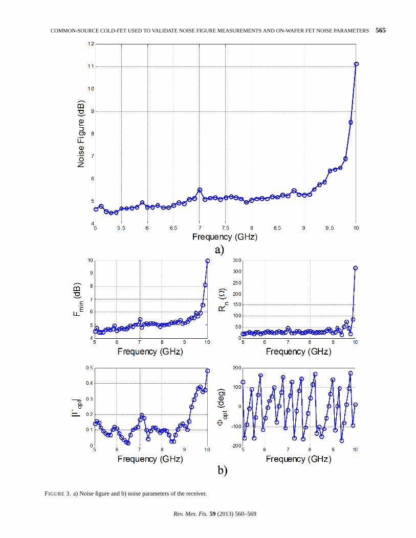
FIGURE 3. a) Noise figure and b) noise parameters of the receiver.
Rev. Mex. Fis.59 (2013) 560–569
566 B. E. FIGUEROA RESENDIZ, M. C. MAYA SANCHEZ, AND J. A. REYNOSO HERNANDEZ
and
Gopt =√
4BC −D2
2B. (36)
The A, B, C and D parameters can be obtained by applyingthe least square method.
3. Experimental results
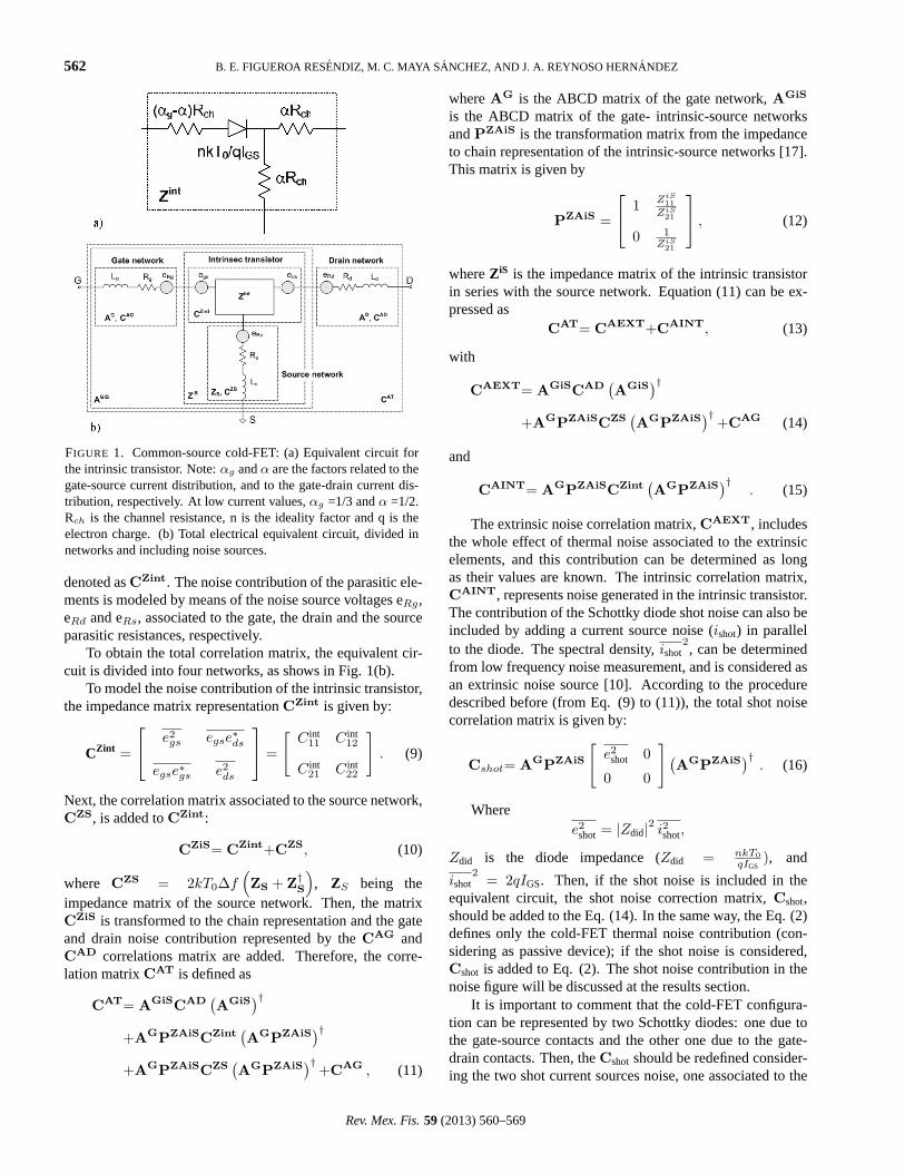
3.1. Noise figure setup
The S-parameters and the noise figure of the device under testhave been measured from 5 to 10 GHz using the experimen-tal setup shown in Fig. 2. The setup consists of a vector net-work analyzer (VNA), a probe station, an input network anda noise receiver. The VNA (HP8510C) is used to measure theS-parameters of the device under test (DUT), and the reflec-tion coefficients of the source, the receiver and the device in-put (denoted asΓS , ΓR andΓin, respectively). The on-waferprobe station (SUMMIT-9000 from Cascade-Microtech) isused as a test fixture for inserting the DUT. The input net-work consists of one switch (SWT1) to select the DUT in-put connection between the VNA or the tuner input, a tuner(focus iCCMT-5020-TC), the VGS bias-tee, and a coplanarmicrowave probe for connecting the DUT input. The noisereceiver consists of a spectrum analyzer (SA) (HP70000 se-ries), a low-noise amplifier (LNA), one switch (SWT2) toselect the output DUT connection between the VNA or theLNA input, an isolator, the VDS bias-tee, and a coplanar mi-crowave probe for connecting the DUT output. All measure-ments are controlled with an external PC via GPIB and Eth-ernet. Prior to measure the device noise figure, the system
noise must be calibrated according to the procedure describedin [19]. While the system noise calibration is performed, athru is connected at the coplanar planes (1-1’and 2-2’) insteadof the DUT. A coaxial HP346C noise source (NS), connectedat the 0-0’plane, is used to calibrate the noise system. In Fig.3(a)-(b) the receiver’s noise figure and its noise parametersare reported. The noise figure is measured with the NS atcold-state [19]. It is important to mention that the isolator isused to avoid reflection between the DUT and the noise re-ceiver. A possible inconvenient of using an isolator is thatthe measurement frequency range is fixed by the operationfrequency of the isolator. This is the reason why the noisefigure measurements shown in Fig. 3(a)-(b) increase at fre-quencies greater than 9 GHz.
3.2. Common-source cold-FET noise figure and noiseparameters
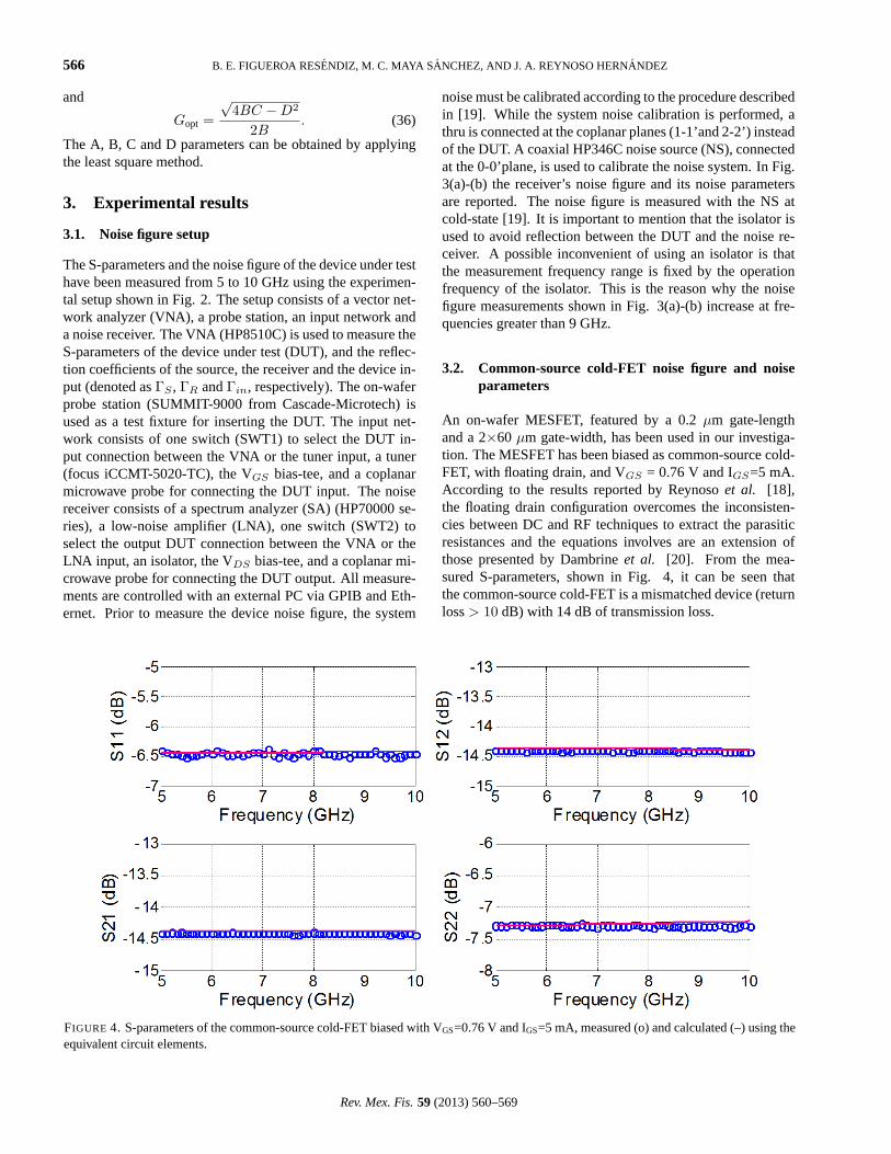
An on-wafer MESFET, featured by a 0.2µm gate-lengthand a 2×60 µm gate-width, has been used in our investiga-tion. The MESFET has been biased as common-source cold-FET, with floating drain, and VGS = 0.76 V and IGS=5 mA.According to the results reported by Reynosoet al. [18],the floating drain configuration overcomes the inconsisten-cies between DC and RF techniques to extract the parasiticresistances and the equations involves are an extension ofthose presented by Dambrineet al. [20]. From the mea-sured S-parameters, shown in Fig. 4, it can be seen thatthe common-source cold-FET is a mismatched device (returnloss> 10 dB) with 14 dB of transmission loss.
FIGURE 4. S-parameters of the common-source cold-FET biased with VGS=0.76 V and IGS=5 mA, measured (o) and calculated (–) using theequivalent circuit elements.
Rev. Mex. Fis.59 (2013) 560–569
COMMON-SOURCE COLD-FET USED TO VALIDATE NOISE FIGURE MEASUREMENTS AND ON-WAFER FET NOISE PARAMETERS567
TABLE I. Equivalent circuit elements of the common-source cold-FET, biased with VGS=0.76V and IGS=5mA
Rg (Ω) 3.47 Lg (pH) 49.05
Rs (Ω) 9.19 Ls (pH) 3.34
Rd (Ω) 11.85 Ld (pH) 76.46
Ideality factor (n) 1.28
The elements value of the equivalent circuit, are extractedaccording to the method described by Reynosoet al. [18],are given in Table I. In Fig. 4 the S-parameters measuredand calculated using the equivalent circuit are compared andgood correlation is observed.
Theoretical values of the common-source cold-FET noisefigure have been computed by applying Eq. (1). The noiseparameters have been extracted with both the F50 and thetuner techniques. To apply the tuner method, different ad-mittance values (Ns >7) have been used to reduce the mea-surements errors [4-8].
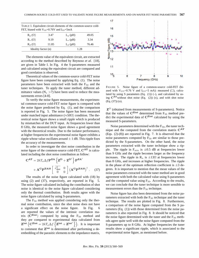
To verify the noise figure measurements, the experimen-tal common-source cold-FET noise figure is compared withthe noise figure predicted by Eq. (1), and the comparisonis reported in Fig. 5. The noise figure has been measuredunder matched input admittance (≈50Ω) condition. The the-oretical noise figure shows a small ripple which is producedby mismatches of the DUT input. At frequencies lower than8 GHz, the measured noise figure shows a good agreementwith the theoretical results. Due to the isolator performance,at higher frequencies the experimental noise figure exhibits aripple whose value oscillates around± 1 dB. This ripple fixesthe accuracy of the measurements.
In order to investigate the shot noise contribution in thenoise figure of the common-source cold-FET,CAT is calcu-lated including the shot noise contribution as follow:
CAT = 2kTa∆fPZAZD + ZD†
PZA†
+ AGPZAiS
[e2
shot 00 0
] (AGPZAiS
)†. (37)
The results of the noise figure calculated with (18) byusing (2) and (37), respectively, are reported in Fig. 5.The noise figure calculated including the contribution of shotnoise is identical to the noise figure calculated consideringonly the thermal contribution. Both results agree with thenoise figure calculated by using S-parameters.
The F50 method was applied considering only the ther-mal noise contribution, since the shot noise does not havea significant effect on the noise figure. In Fig. 6are reported the values of the intrinsic correlation ma-trix (CZint) computed by using the F50 method andthey are compared to experimental data calculated fromZint
(CZint = 2kTa∆f
Zint + Zint†
). It is important
to comment thatZint is determined after performing a de-embedding of the parasitic elements to the impedance matrix,
FIGURE 5. Noise figure of a common-source cold-FET (bi-ased with VGS=0.76 V and IGS=5 mA): measured (¤), calcu-lated by using S parameters (Eq. (1)) (–), and calculated by us-ing CATwithout shot noise (Eq. (2)) (x), and with shot noise(Eq. (37)) (o).
ZD (obtained from measurements of S-parameters). Noticethat the values ofCZint determined from F50 method pre-dict the experimental data ofCZint calculated by using themeasured S-parameters.
Noise parameters determined with the F50, the tuner tech-nique and the computed from the correlation matrixCAT
(Eqs. (2)-(8)) are reported in Fig. 7. It is observed that thenoise parameters computed by F50 are similar to those pre-dicted by the S-parameters. On the other hand, the noiseparameters extracted with the tuner technique show a rip-ple. The ripple in Fmin is ±0.5 dB at frequencies lowerthan 9 GHz and the ripple becomes larger as the frequencyincreases. The ripple in Rn is ±13Ω at frequencies lowerthan 8 GHz, and increases at higher frequencies. The ripplein the phase of the optimum reflection coefficient is±3 de-grees. It is important to mention that the mean values of thenoise parameters extracted with the tuner method are in goodagreement with both the calculated value using S-parametersand the computed value using F50. According to the results,we can conclude that the tuner technique is more sensible tomeasurement errors than the F50 technique.
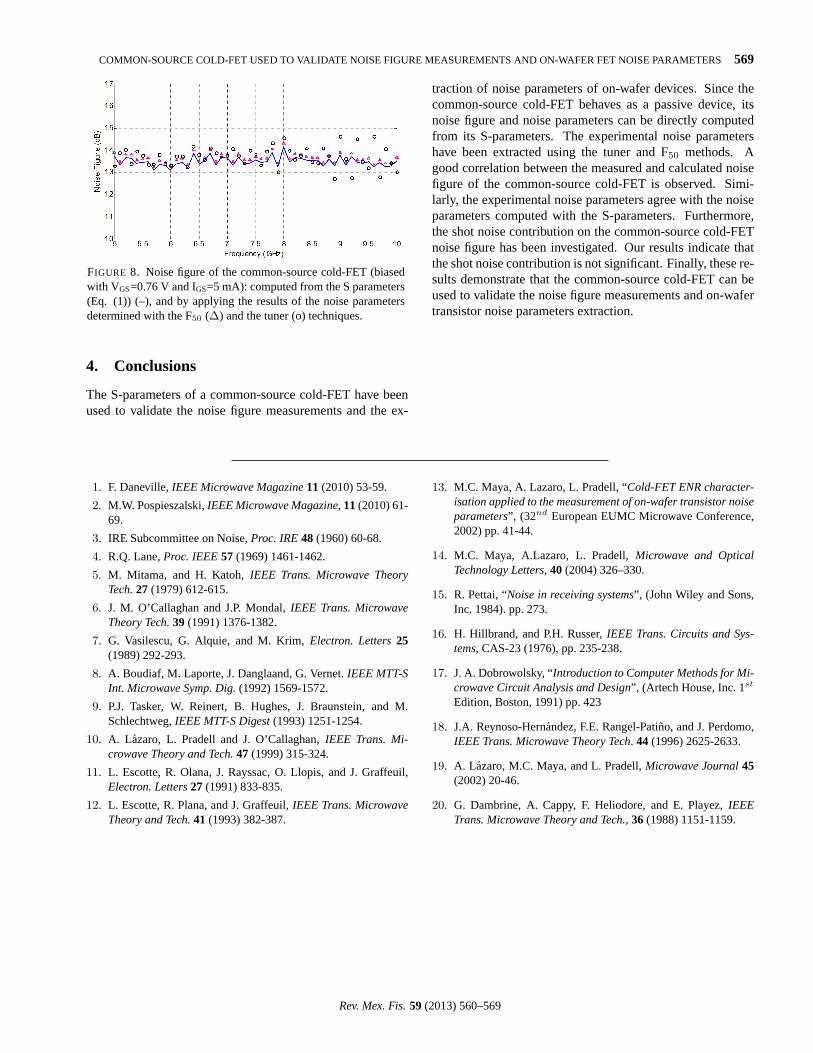
Noise figure has also been determined from the noise pa-rameters extracted with both the F50 technique and the tunertechnique. The results are plotted in Fig. 8. Furthermore,a comparison of the noise figure computed from the S pa-rameters (Eq. (1)) with those determined from the noise pa-rameters is also reported in Fig. 8. It should be noticed thatthe noise figure determined with the tuner and the F50 meth-ods agree quite well with the noise figure computed from theS-parameters up to 8 GHz. At higher frequencies the tunerresults show a significant ripple, which is associated to theexperimental noise figure, as mentioned before.
Rev. Mex. Fis.59 (2013) 560–569
568 B. E. FIGUEROA RESENDIZ, M. C. MAYA SANCHEZ, AND J. A. REYNOSO HERNANDEZ
FIGURE 6. Elements of the intrinsic correlation matrix: (–) computed from F50 and by using (o) the S-parameters.
FIGURE 7. Common-source cold-FET’s noise parameters: theoretical (computed from the S parameters (–)) and extracted with the F50(∆),and tuner (o) techniques. The cold-FET has been biased with VGS=0.76 V and IGS=5 mA.
Rev. Mex. Fis.59 (2013) 560–569
COMMON-SOURCE COLD-FET USED TO VALIDATE NOISE FIGURE MEASUREMENTS AND ON-WAFER FET NOISE PARAMETERS569
FIGURE 8. Noise figure of the common-source cold-FET (biasedwith VGS=0.76 V and IGS=5 mA): computed from the S parameters(Eq. (1)) (–), and by applying the results of the noise parametersdetermined with the F50 (∆) and the tuner (o) techniques.
4. Conclusions
The S-parameters of a common-source cold-FET have beenused to validate the noise figure measurements and the ex-
traction of noise parameters of on-wafer devices. Since thecommon-source cold-FET behaves as a passive device, itsnoise figure and noise parameters can be directly computedfrom its S-parameters. The experimental noise parametershave been extracted using the tuner and F50 methods. Agood correlation between the measured and calculated noisefigure of the common-source cold-FET is observed. Simi-larly, the experimental noise parameters agree with the noiseparameters computed with the S-parameters. Furthermore,the shot noise contribution on the common-source cold-FETnoise figure has been investigated. Our results indicate thatthe shot noise contribution is not significant. Finally, these re-sults demonstrate that the common-source cold-FET can beused to validate the noise figure measurements and on-wafertransistor noise parameters extraction.
1. F. Daneville,IEEE Microwave Magazine11 (2010) 53-59.
2. M.W. Pospieszalski,IEEE Microwave Magazine,11(2010) 61-69.
3. IRE Subcommittee on Noise,Proc. IRE48 (1960) 60-68.
4. R.Q. Lane,Proc. IEEE57 (1969) 1461-1462.
5. M. Mitama, and H. Katoh,IEEE Trans. Microwave TheoryTech.27 (1979) 612-615.
6. J. M. O’Callaghan and J.P. Mondal,IEEE Trans. MicrowaveTheory Tech.39 (1991) 1376-1382.
7. G. Vasilescu, G. Alquie, and M. Krim,Electron. Letters25(1989) 292-293.
8. A. Boudiaf, M. Laporte, J. Danglaand, G. Vernet.IEEE MTT-SInt. Microwave Symp. Dig.(1992) 1569-1572.
9. P.J. Tasker, W. Reinert, B. Hughes, J. Braunstein, and M.Schlechtweg,IEEE MTT-S Digest(1993) 1251-1254.
10. A. Lazaro, L. Pradell and J. O’Callaghan,IEEE Trans. Mi-crowave Theory and Tech.47 (1999) 315-324.
11. L. Escotte, R. Olana, J. Rayssac, O. Llopis, and J. Graffeuil,Electron. Letters27 (1991) 833-835.
12. L. Escotte, R. Plana, and J. Graffeuil,IEEE Trans. MicrowaveTheory and Tech.41 (1993) 382-387.
13. M.C. Maya, A. Lazaro, L. Pradell, “Cold-FET ENR character-isation applied to the measurement of on-wafer transistor noiseparameters”, (32nd European EUMC Microwave Conference,2002) pp. 41-44.
14. M.C. Maya, A.Lazaro, L. Pradell,Microwave and OpticalTechnology Letters, 40 (2004) 326–330.
15. R. Pettai, “Noise in receiving systems”, (John Wiley and Sons,Inc. 1984). pp. 273.
16. H. Hillbrand, and P.H. Russer,IEEE Trans. Circuits and Sys-tems, CAS-23 (1976), pp. 235-238.
17. J. A. Dobrowolsky, “Introduction to Computer Methods for Mi-crowave Circuit Analysis and Design”, (Artech House, Inc. 1st
Edition, Boston, 1991) pp. 423
18. J.A. Reynoso-Hernandez, F.E. Rangel-Patino, and J. Perdomo,IEEE Trans. Microwave Theory Tech. 44 (1996) 2625-2633.
19. A. Lazaro, M.C. Maya, and L. Pradell,Microwave Journal45(2002) 20-46.
20. G. Dambrine, A. Cappy, F. Heliodore, and E. Playez,IEEETrans. Microwave Theory and Tech., 36 (1988) 1151-1159.
Rev. Mex. Fis.59 (2013) 560–569