Embed Size (px)
Citation preview
1
Common-mode Voltage Reduction for MatrixConverters Using All Valid Switch States
Quanxue Guan, Student Member, IEEE, Patrick Wheeler, Senior Member, IEEE,Quansheng Guan, Member, IEEE, and Ping Yang Member, IEEE,
Abstract—This paper presents a new space vector modulation(SVM) strategy for matrix converters to reduce the common-mode voltage (CMV). The reduction is achieved by using theswitch configurations that connect each input phase to a differentoutput phase, or the configurations that connect all the outputphases to the input phase with minimum absolute voltage. Thesetwo types of configurations always produce lower peak CMV thanthe others, especially the former ones that result in zero CMVat the output side of matrix converters. In comparison with theexisting SVM methods, this strategy has a very similar softwareoverhead and calculation time. Simulation and experiment resultsare shown to validate the effectiveness of the proposed modulationmethod in reducing not only the peak value but also the rootmean square value of the CMV.
Index Terms—Common-mode Voltage, Matrix Converters, Sin-gular Value Decomposition, Space Vector Modulation.
I. INTRODUCTION
THE matrix converter (MC) has been a promising powerconverter topology during the past decades [1], [2]. The
main reason for this interest lies in the potential advantagesof MCs, such as direct conversion, controllable input displace-ment factor, bi-directional power flow and high power density.
The modulation algorithm is one of the important factors indetermining the performance of MCs. The existing modulationalgorithms for MCs are intrinsically based on the well-knownpulse-width modulation (PWM) [3]. As a result of the PWMswitching pattern, MC generates a series of staircase-like highfrequency common-mode voltage (CMV) waveforms. SimilarCMV also appears in three-phase inverters [4]–[6]. Large mag-nitude and high frequency variation of CMV, unfortunately,have been known as the root causes of early motor windingfailure and machine bearing deterioration [7].
Different methods have been reported to mitigate the detri-mental influences of the CMV for MCs. An intuitive idea is
Manuscript received August 23, 2014; revised July 08, 2015, September 18,2015 and November 14, 2015; accepted January 05, 2016. Date of publicationXXX.XX, 2016; date of current version January 20, 2016. This work wassupported in part by the National Natural Science Foundation of China underGrant 61302058 and Grant 61431005, and in part by Guangzhou Elite OverseaStudy Program under Grant JY201323.
Quanxue Guan is with the School of Electronic and Information Engineer-ing and School of Electric Power, South China University of Technology,Guangzhou, 510640, P.R.China (e-mail: [email protected]).
P. W. Wheeler is with the Department of Electrical and Electronic En-gineering, University of Nottingham, Nottingham, NG7 2RD, U.K. (e-mail:[email protected]).
Quansheng Guan is with the School of Electronic and Information Engineer-ing, South China University of Technology, Guangzhou, 510640, P.R.China (e-mail: [email protected]). Quansheng Guan is the corresponding author.
Ping Yang is with the School of Electric Power, South China University ofTechnology, Guangzhou, 510640, P.R.China (e-mail: [email protected]).
using only the rotating vectors that correspond to the switchconfigurations with zero CMV in dual structure converters [8]–[16]. This technique has been applied to direct and indirect MCfed open-end winding AC drives to reduce or even eliminatethe CMV. However, it is not considered in this paper owingto the increased costs and control complexities introduced byadditional power semiconductor devices.
Methods exist that modify modulation strategies to reducethe magnitude of the CMV issues [17]–[30]. Since the CMVis brought about by the input voltages together with differentswitch configurations, it is preferable to choose those with lowpeak CMVs and low voltage transitions whenever possible. Inthe space vector modulation (SVM) algorithms for MCs [31]–[33], switch configurations are selected under the criterion ofminimizing the switching count. Therefore, four active switchconfigurations and one zero switch configuration (ZSC) areselected in each sampling period. In order to reduce the CMV,two active vectors with opposite directions or three nearest-state vectors were chosen instead during the time intervals forthe zero vectors in [17]–[23]. Unfortunately, these methods usemore than five switch configurations in each sampling period,thus increase the switching power losses. Besides, the lattermethod can be applied only when the voltage transfer ratio(VTR) is larger than 0.667 [23]. When the VTR is smallerthan 0.5, Hong-Hee Lee et al. also put forward several CMV-reduced strategies using two adjacent vectors with 120-phaseshift to reduce the duty cycles for zero vectors [20]–[25]. Fromthe perspective of CMV reduction, however, it is unnecessaryto exclude all ZSCs, because the CMV peak of the zero vectorconnecting to the input phase that is with the medium voltagevalue is lower than those of active vectors [26]–[30].
Note that for a three-phase-to-three-phase direct MC, theswitch configurations that connect each input to one differentoutput phase have zero CMV. The corresponding voltage vec-tors of these switch configurations have been often referred toas the “rotating vectors”. In this context, the perhaps more ap-propriate name is given for this type of switch configurations,i.e. “Orientation Switch Configuration” (OSC). Nevertheless,they are regarded to be trivial in the literature [31]–[33]. It isdifficult to calculate their duty cycles and arrange them in theswitching sequence [34]–[42]. For example, Yugo Tadano etal. tried to use these switch configurations though at the costof complex switch pattern selection [39], [40]. Jordi Espinaet al. proposed an SVM method to replace the three ZSCsby three OSCs with same rotating direction and equal dutycycle [41]. However, it is difficult to arrange proper switchingsequences to achieve safe commutation by using three ZSCs.
2
Without the need of modulation, Rene Vargas et al. addeda term in the quality function of the predictive model tosuppress the CMV [43]–[46]. However, this method has a highcomputational overhead.
To use the OSCs in the modulation, we first investigate allvalid switch configurations by applying the singular value de-composition (SVD) on their space vector representations [47].The geometrical meaning of SVD can reveal how each switchconfiguration transforms a column vector between differentreference frames. Thus, it provides an insight on the intrinsicproperties of the switch configurations. These switch config-urations are then categorized into three types according totheir SVD results. The relationships between different switchconfigurations are also found so that the OSCs can be usedeasily by equivalent decomposition and combination.
We further propose a CMV-reduced modulation algorithmfor MCs, taking advantage of all valid switch configurations,especially the OSCs. The proposed algorithm is divided intotwo VTR regions. For high VTRs, one OSC is incorporate ineach sampling period by replacing its equivalent switch con-figurations. For low VTRs, one ZSC connecting to the inputphase that is with the medium voltage value is used instead ofthe OSC. Therefore, by using the switch configurations withlower CMV amplitude, not only the peak value but also theroot mean square (RMS) of the output CMV are reduced.Also worth mentioning is that the transition between the highand low VTR regions is smoothly achieved according to thecomparison of the calculated duty cycles.
Although our proposed method is based on the traditionalSVM method, it does not increase the computation burdennoticeably. The calculation time increases by less than 6%from 82.84µs to the 87.64µs. This is because that the inclusionof the OSCs and ZSCs in our CMV-reduced SVM method isintroduced by equivalent substitution. Once the duty cyclesutilized in the traditional SVM algorithms are calculated, onlyminor comparison and addition operations are required forthe proposed method. In addition, unlike the other algorithmsin [34]–[46] that also use the OSCs, our proposed method cansynthesize the reference variables without the measurement ofoutput currents. Hence, no extra components are involved.
II. MATRIX CONVERTER SYSTEM MODEL
A three-phase-to-three-phase direct MC consists of a nine-switch array, as shown in Fig. 1. By modeling each switchas an ideal switching function whose value is one when theswitch is conducting and zero when the switch is blocking,the voltage relationship between the input and the output ofthe MC can be expressed as follows [48],
Vo=
vAvBvC
=
SAa SAb SAcSBa SBb SBcSCa SCb SCc
vavbvc
=SVi, (1)
where the switch state matrix (SSM) S represents the connect-ing configuration within the MC array. Similarly, the currentrelationship can be formulated as Ii = ST Io, where the super-script “T” means the transpose operation. The input voltagesand output currents are considered as the input variables of theMC. Typically, the input side source is a voltage type since the
a
b
cA B C
AaS BaS CaS
AbS BbS CbS
AcS BcS CcS
0ai
bi
ci
0av
0bv
0cv
Ai Bi CiABv BCv
CAv
fC
Inductive Loads
fL
hkS
DSP
Digital Controller
/FPGA CPLD
Sensors
Sensors
CMLeakage Current i
Fig. 1. Three-phase direct matrix converter topology.
MC is connected to the grid or LC filter, while the output isa current source because the MC is feeding an inductive load.Due to the nature of different sources that the MC is connectedto, short circuits between the input terminals meanwhile opencircuits at the output ports are prohibited. As a consequence,only 27 different switch configurations are allowed under theconstraints for safe operations, which can also be representedas SKa + SKb + SKc = 1, for K = A,B,C.
In order to simplify the analysis, (1) is transformed fromthe abc coordinate into the αβ reference frame, represented inthe space vector form as Vo,αβ0 = TST−1Vi,αβ0, using themodified Clark Transformation [33]–[38]
T =
√2
3
1 − 12 − 1
2
0√32 −
√32
1√2
1√2
1√2
. (2)
The zero sequence current does not exist in the three-phasethree-wire systems. Therefore, the voltage relationship can beexpressed in matrix form by ignoring the zero component [47],[
voαvoβ
]=
[S1α S1β
S2β S2α
] [viαviβ
]= Sxyz
[viαviβ
], (3)
where Sxyz is the space vector representation of the transfermatrix S in (1), and xyz stands for the input phases that areconnected to the output ones. For example, when the outputphases ABC are linked in order to the input phases abb, Sxyzcan be written as Sabb. The input and output voltage spacevectors can also be expressed as ~vi = Viα + jViβ and ~vo =Voα + jVoβ respectively.
III. SINGULAR-VALUE-DECOMPOSITION-BASED SPACEVECTOR MODULATION
To show how the SSM transforms the input voltage betweenthe input and output coordinates, Sxyz in (3) is factorized bythe SVD into the multiplication of three matrices, representingas Sxyz = U∗D∗VT , where U and V are unitary matricesand D is a diagonal matrix with σd and σq being the diagonalelements. Geometrically, matrix V denotes a rotation or reflec-tion operation to the input space vector with respect to the realaxis of input side, while D indicates scaling operation along
3
the orthonormal coordinate axes with σd and σq representingthe axis gains. Subsequently, matrix U rotates the intermediatevector that results from the product of input column vector,VT and D, by another angle to obtain the output voltagespace vector. Note that the transpose of a rotation matrix meansrotating in reverse.
With the output phases ABC connected to the input phasesabb respectively as an example, the space vector representedtransfer matrix Sabb can be calculated and decomposed:
Sabb =
[1 −
√33
0 0
]=
[1 00 1
] [ 2√3
0
0 0
][ √32
12
− 12
√32
]T. (4)
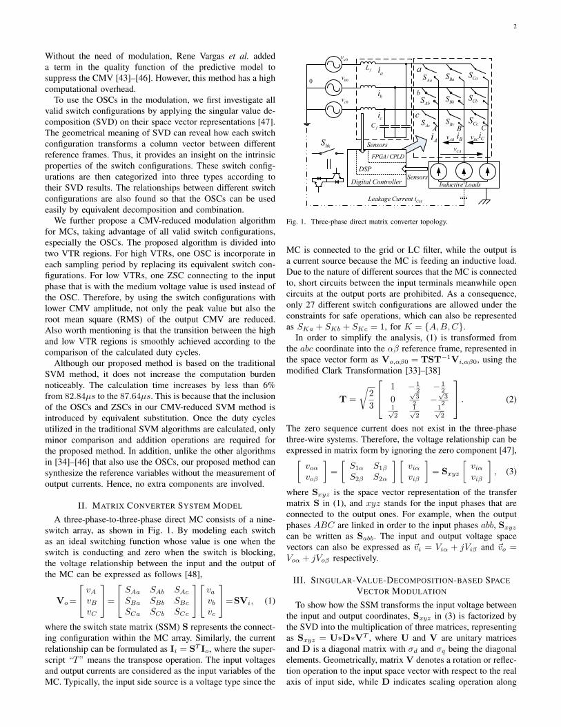
All valid switch configurations can be categorized into threetypes according to the SVD results of their space vectorrepresentation, as listed in Table I.• Type I: Zero Switch Configuration (ZSC). The ZSCs
connect all output lines to the same input phase and henceresult in zero voltage space vectors since the output linevoltages are zero. For this type of switch configurations,the diagonal elements in the matrices Ds are all zero.
• Type II: Rotation Switch Configuration (RSC). The RSCsconnect two output lines to a common input phase, andconnect the remaining output line to one of the other inputphases. All their factorized Us and Vs are special unitarymatrices, i.e. rotation matrices. Besides, the secondarydiagonal elements in matrices Ds are zero. It is importantto point out that the rotation angles of Us and Vsare determined only by the switch configurations, butindependent of the MC inputs. If these rotation matricesare represented as their equivalent rotation vectors withsame angles, two unit hexagons depicting Us and Vsrespectively can be found, as shown in Fig. 2. Bothhexagons are different from those in the traditional SVM,where the switch configurations are considered togetherwith the input voltages or output currents, and thus theresultant output voltage and input current space vectorshave fixed angles but variable amplitudes [49]. Type IIswitch configurations are also summarized in Table II,with the rotation angles of their decomposed Us and Vsmatching the positions of their equivalent rotation vectorsin different hexagons of Fig. 2.
• Type III: Orientation Switch Configuration (OSC). For theaforementioned OSCs, one of their factorized matrices (Vin this paper) determines the orientation, i.e. clock-wiseor counter-clock-wise, or the positive rotation directionof the resultant rotating output voltages. In three-phasesystems, this means to determine whether the coordinateis left-handed or right-handed. Corresponding to the tra-ditional SVM, they result in rotating output voltage spacevectors with fixed amplitudes since unitary matrices areisometry, but with variable angles depending on both theswitch configurations and the input voltages. In addition,the matrices Ds for OSCs are Identity Matrices.
All the q-axis gains of the ZSCs and RSCs are equal tozero. This feature brings facilitation to synthesize the referenceoutput voltage and input current vectors. Suppose that thedesired transfer function is
TABLE ISINGULAR VALUE DECOMPOSITION RESULTS OF ALL VALID SPACE VECTOR
REPRESENTED TRANSFER MATRICES
SSMSV D
U D V
I Sxxx
[0 00 0
] [1 00 1
] [0 00 0
] [1 00 1
]
II1
Sabb
[1 −
√3
30 0
] [1 00 1
] [2√3
0
0 0
] √32
12
−12
√3
2
Scbb
[0 − 2
√3
30 0
] [1 00 1
] [2√3
0
0 0
] [0 1−1 0
]
Scaa
[−1 −
√3
30 0
] [1 00 1
] [2√3
0
0 0
] −√32
12
−12−√
32
Sbaa
[−1
√3
30 0
] [1 00 1
] [2√3
0
0 0
] −√32
−12
12
−√
32
Sbcc
[0 2
√3
30 0
] [1 00 1
] [2√3
0
0 0
] [0 −11 0
]
Sacc
[1
√3
30 0
] [1 00 1
] [2√3
0
0 0
] √32− 1
212
√3
2
II2
Sbab
− 12
√3
6√3
2− 1
2
−12−√
32√
32
−12
[2√3
0
0 0
] √32
12
−12
√3
2
Sbcb
[0
√3
30 −1
] −12−√
32√
32
−12
[2√3
0
0 0
] [0 1−1 0
]
Saca
12
√3
6
−√
32
− 12
−12−√
32√
32
−12
[2√3
0
0 0
] −√32
12
−12−√
32
Saba
12
−√
36
−√
32
12
−12−√
32√
32
−12
[2√3
0
0 0
] −√32
−12
12
−√
32
Scbc
[0 −
√3
30 1
] −12−√
32√
32
−12
[2√3
0
0 0
] [0 −11 0
]
Scac
− 12
−√
36√
32
12
−12−√
32√
32
−12
[2√3
0
0 0
] √32− 1
212
√3
2
II3
Sbba
− 12
√3
6
−√
32
12
−12
√3
2
−√
32
−12
[2√3
0
0 0
] √32
12
−12
√3
2
Sbbc
[0
√3
30 1
] −12
√3
2
−√
32
−12
[2√3
0
0 0
] [0 1−1 0
]
Saac
12
√3
6√3
212
−12
√3
2
−√
32
−12
[2√3
0
0 0
] −√32
12
−12−√
32
Saab
12
−√
36√
32
− 12
−12
√3
2
−√
32
−12
[2√3
0
0 0
] −√32
−12
12
−√
32
Sccb
[0 −
√3
30 −1
] −12
√3
2
−√
32
−12
[2√3
0
0 0
] [0 −11 0
]
Scca
− 12
−√
36
−√
32
− 12
−12
√3
2
−√
32
−12
[2√3
0
0 0
] √32− 1
212
√3
2
III
Sabc
[1 00 1
] [1 00 1
] [1 00 1
] [1 00 1
]Scab
− 12
−√
32√
32
− 12
−12−√
32√
32
−12
[1 00 1
] [1 00 1
]
Sbca
− 12
√3
2
−√
32
− 12
−12
√3
2
−√
32
−12
[1 00 1
] [1 00 1
]Sacb
[1 00 −1
] [1 00 1
] [1 00 1
] [1 00 −1
]Sbac
− 12
√3
2√3
212
−12−√
32√
32
−12
[1 00 1
] [1 00 −1
]
Scba
− 12−√
32
−√
32
12
−12
√3
2
−√
32
−12
[1 00 1
] [1 00 −1
]1 xxx stands for aaa, bbb or ccc.
U∗D∗VT=
[cosα −sinαsinα cosα
][gd 00 gq
][cos θ −sin θsin θ cos θ
]T, (5)
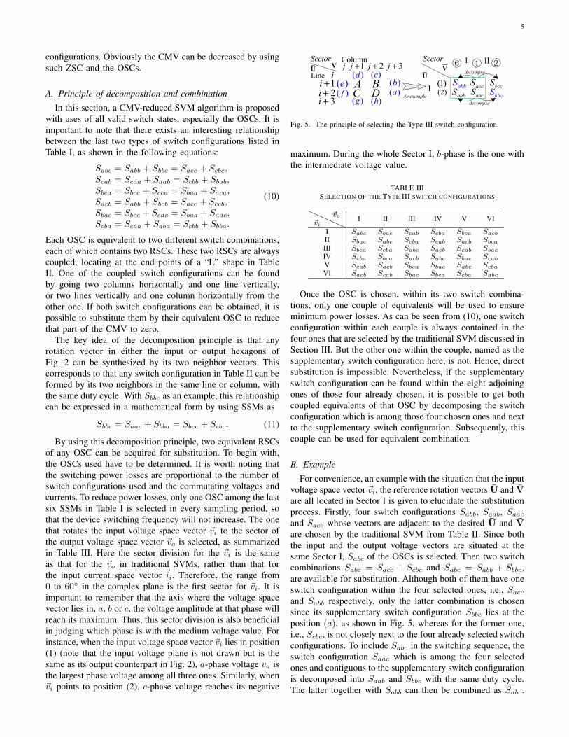
it is easy to synthesize these continuous modulation matricesusing only the first two types of switch configurations, accord-ing to the high-frequency synthesis [50]. Here U, D and V arethe local averaged values of U, D, and V respectively withrespect to their duty cycles within one switching period. Sinceσq ≡ 0, the q-axis averaged gain gq equals to zero. Hence, theoutput voltage reference ~vo is always located in the d-axis ofthe rotation matrix U, while the input current reference ~ii isalways placed in the d-axis of the rotation matrix V, as shownin Fig. 3. The rotation angle θ of V is exactly the angle of
4
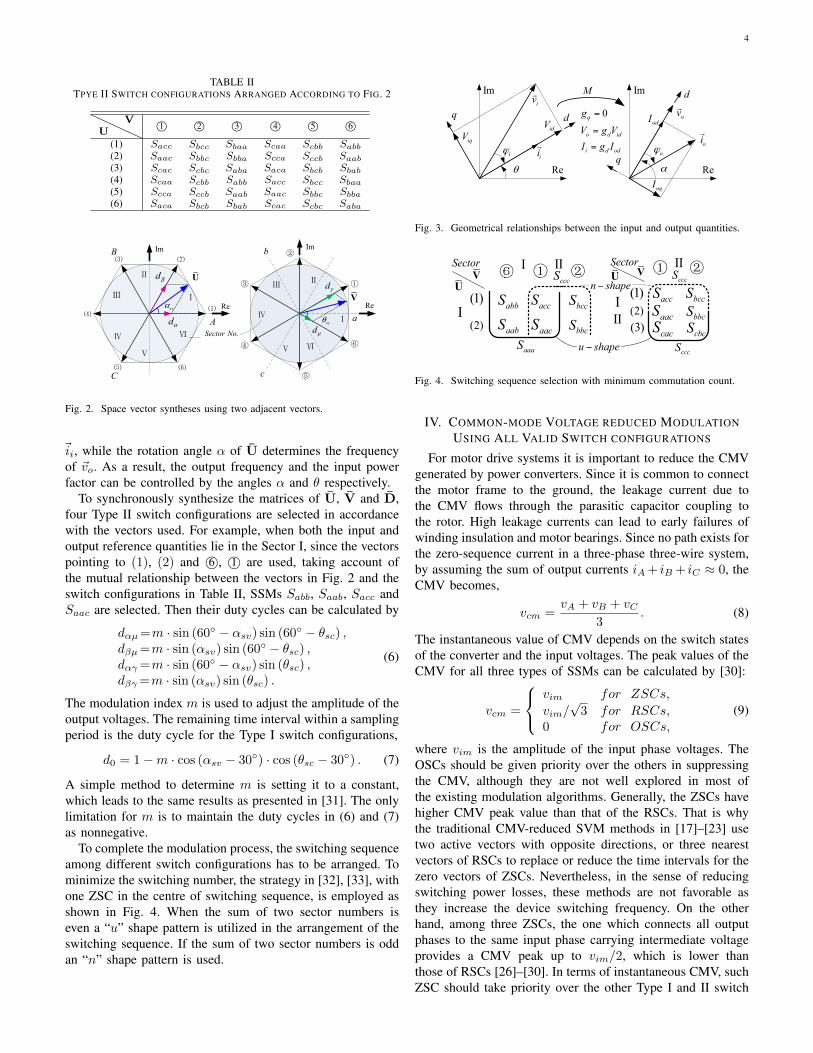
TABLE IITPYE II SWITCH CONFIGURATIONS ARRANGED ACCORDING TO FIG. 2
UV
1© 2© 3© 4© 5© 6©
(1) Sacc Sbcc Sbaa Scaa Scbb Sabb(2) Saac Sbbc Sbba Scca Sccb Saab(3) Scac Scbc Saba Saca Sbcb Sbab(4) Scaa Scbb Sabb Sacc Sbcc Sbaa(5) Scca Sccb Saab Saac Sbbc Sbba(6) Saca Sbcb Sbab Scac Scbc Saba
①
②
③
④
⑤
⑥
Ⅰ
ⅡⅢ
Ⅳ
Ⅴ Ⅵ
Ⅰ
Ⅱ
Ⅲ
Ⅳ
Ⅴ
Ⅵ
⑴
⑵⑶
⑷
⑸ ⑹
Udβ
dα
Vdγ
dµscθ
svα
.Sector No
Re
Im
Re
Im
a
b
c
A
B
C
Fig. 2. Space vector syntheses using two adjacent vectors.
~ii, while the rotation angle α of U determines the frequencyof ~vo. As a result, the output frequency and the input powerfactor can be controlled by the angles α and θ respectively.
To synchronously synthesize the matrices of U, V and D,four Type II switch configurations are selected in accordancewith the vectors used. For example, when both the input andoutput reference quantities lie in the Sector I, since the vectorspointing to (1), (2) and 6©, 1© are used, taking account ofthe mutual relationship between the vectors in Fig. 2 and theswitch configurations in Table II, SSMs Sabb, Saab, Sacc andSaac are selected. Then their duty cycles can be calculated by
dαµ=m · sin (60 − αsv) sin (60 − θsc) ,dβµ=m · sin (αsv) sin (60 − θsc) ,dαγ =m · sin (60 − αsv) sin (θsc) ,dβγ =m · sin (αsv) sin (θsc) .
(6)
The modulation index m is used to adjust the amplitude of theoutput voltages. The remaining time interval within a samplingperiod is the duty cycle for the Type I switch configurations,
d0 = 1−m · cos (αsv − 30) · cos (θsc − 30) . (7)
A simple method to determine m is setting it to a constant,which leads to the same results as presented in [31]. The onlylimitation for m is to maintain the duty cycles in (6) and (7)as nonnegative.
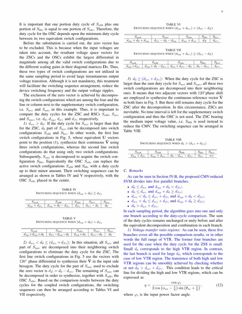
To complete the modulation process, the switching sequenceamong different switch configurations has to be arranged. Tominimize the switching number, the strategy in [32], [33], withone ZSC in the centre of switching sequence, is employed asshown in Fig. 4. When the sum of two sector numbers iseven a “u” shape pattern is utilized in the arrangement of theswitching sequence. If the sum of two sector numbers is oddan “n” shape pattern is used.
θ
iϕ
iv!
idViqV
ii!
α
oϕ
ov!
odI
oi!
d
q
dq
oqI
0q
o d id
i d od
gV g VI g I
=
=
=
M
Re
Im
Re
Im
Fig. 3. Geometrical relationships between the input and output quantities.
abbS
aabS
cccS
aacSbccS
bbcS
(1)
(2)
Sector
aaaS
accS
u shape−
n shape−⑥
I
① ②I II
UV
aacSbccSbbcS
(1)(2)
Sector
accSI
① ②IIU V
cacS cbcS(3)
cccS
II
cccS
Fig. 4. Switching sequence selection with minimum commutation count.
IV. COMMON-MODE VOLTAGE REDUCED MODULATIONUSING ALL VALID SWITCH CONFIGURATIONS
For motor drive systems it is important to reduce the CMVgenerated by power converters. Since it is common to connectthe motor frame to the ground, the leakage current due tothe CMV flows through the parasitic capacitor coupling tothe rotor. High leakage currents can lead to early failures ofwinding insulation and motor bearings. Since no path exists forthe zero-sequence current in a three-phase three-wire system,by assuming the sum of output currents iA+ iB + iC ≈ 0, theCMV becomes,
vcm =vA + vB + vC
3. (8)
The instantaneous value of CMV depends on the switch statesof the converter and the input voltages. The peak values of theCMV for all three types of SSMs can be calculated by [30]:
vcm =
vim for ZSCs,
vim/√
3 for RSCs,0 for OSCs,
(9)
where vim is the amplitude of the input phase voltages. TheOSCs should be given priority over the others in suppressingthe CMV, although they are not well explored in most ofthe existing modulation algorithms. Generally, the ZSCs havehigher CMV peak value than that of the RSCs. That is whythe traditional CMV-reduced SVM methods in [17]–[23] usetwo active vectors with opposite directions, or three nearestvectors of RSCs to replace or reduce the time intervals for thezero vectors of ZSCs. Nevertheless, in the sense of reducingswitching power losses, these methods are not favorable asthey increase the device switching frequency. On the otherhand, among three ZSCs, the one which connects all outputphases to the same input phase carrying intermediate voltageprovides a CMV peak up to vim/2, which is lower thanthose of RSCs [26]–[30]. In terms of instantaneous CMV, suchZSC should take priority over the other Type I and II switch
5
configurations. Obviously the CMV can be decreased by usingsuch ZSC and the OSCs.
A. Principle of decomposition and combination
In this section, a CMV-reduced SVM algorithm is proposedwith uses of all valid switch states, especially the OSCs. It isimportant to note that there exists an interesting relationshipbetween the last two types of switch configurations listed inTable I, as shown in the following equations:
Sabc = Sabb + Sbbc = Sacc + Scbc,Scab = Scaa + Saab = Scbb + Sbab,Sbca = Sbcc + Scca = Sbaa + Saca,Sacb = Sabb + Sbcb = Sacc + Sccb,Sbac = Sbcc + Scac = Sbaa + Saac,Scba = Scaa + Saba = Scbb + Sbba.
(10)
Each OSC is equivalent to two different switch combinations,each of which contains two RSCs. These two RSCs are alwayscoupled, locating at the end points of a “L” shape in TableII. One of the coupled switch configurations can be foundby going two columns horizontally and one line vertically,or two lines vertically and one column horizontally from theother one. If both switch configurations can be obtained, it ispossible to substitute them by their equivalent OSC to reducethat part of the CMV to zero.
The key idea of the decomposition principle is that anyrotation vector in either the input or output hexagons ofFig. 2 can be synthesized by its two neighbor vectors. Thiscorresponds to that any switch configuration in Table II can beformed by its two neighbors in the same line or column, withthe same duty cycle. With Sbbc as an example, this relationshipcan be expressed in a mathematical form by using SSMs as
Sbbc = Saac + Sbba = Sbcc + Scbc. (11)
By using this decomposition principle, two equivalent RSCsof any OSC can be acquired for substitution. To begin with,the OSCs used have to be determined. It is worth noting thatthe switching power losses are proportional to the number ofswitch configurations used and the commutating voltages andcurrents. To reduce power losses, only one OSC among the lastsix SSMs in Table I is selected in every sampling period, sothat the device switching frequency will not increase. The onethat rotates the input voltage space vector ~vi to the sector ofthe output voltage space vector ~vo is selected, as summarizedin Table III. Here the sector division for the ~vi is the sameas that for the ~vo in traditional SVMs, rather than that forthe input current space vector ~ii. Therefore, the range from0 to 60 in the complex plane is the first sector for ~vi. It isimportant to remember that the axis where the voltage spacevector lies in, a, b or c, the voltage amplitude at that phase willreach its maximum. Thus, this sector division is also beneficialin judging which phase is with the medium voltage value. Forinstance, when the input voltage space vector ~vi lies in position(1) (note that the input voltage plane is not drawn but is thesame as its output counterpart in Fig. 2), a-phase voltage va isthe largest phase voltage among all three ones. Similarly, when~vi points to position (2), c-phase voltage reaches its negative
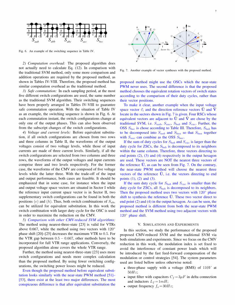
AC
Sector
BD
2j + 3j +
3i +
i1i +2i + ( )a
( )b( )c( )d
( )e( )f
( )g ( )h
jLine
ColumnU V 1j +
abbSaabS
Sector
accSaacS
⑥ ① ②I II
(1)(2)I
UV
bbcSbccS
decompse
decompseAn example
Fig. 5. The principle of selecting the Type III switch configuration.
maximum. During the whole Sector I, b-phase is the one withthe intermediate voltage value.
TABLE IIISELECTION OF THE TYPE III SWITCH CONFIGURATIONS
~vi
~vo I II III IV V VI
I Sabc Sbac Scab Scba Sbca SacbII Sbac Sabc Scba Scab Sacb SbcaIII Sbca Scba Sabc Sacb Scab SbacIV Scba Sbca Sacb Sabc Sbac ScabV Scab Sacb Sbca Sbac Sabc ScbaVI Sacb Scab Sbac Sbca Scba Sabc
Once the OSC is chosen, within its two switch combina-tions, only one couple of equivalents will be used to ensureminimum power losses. As can be seen from (10), one switchconfiguration within each couple is always contained in thefour ones that are selected by the traditional SVM discussed inSection III. But the other one within the couple, named as thesupplementary switch configuration here, is not. Hence, directsubstitution is impossible. Nevertheless, if the supplementaryswitch configuration can be found within the eight adjoiningones of those four already chosen, it is possible to get bothcoupled equivalents of that OSC by decomposing the switchconfiguration which is among those four chosen ones and nextto the supplementary switch configuration. Subsequently, thiscouple can be used for equivalent combination.
B. Example
For convenience, an example with the situation that the inputvoltage space vector ~vi, the reference rotation vectors U and Vare all located in Sector I is given to elucidate the substitutionprocess. Firstly, four switch configurations Sabb, Saab, Saacand Sacc whose vectors are adjacent to the desired U and Vare chosen by the traditional SVM from Table II. Since boththe input and the output voltage vectors are situated at thesame Sector I, Sabc of the OSCs is selected. Then two switchcombinations Sabc = Sacc + Scbc and Sabc = Sabb + Sbbc,are available for substitution. Although both of them have oneswitch configuration within the four selected ones, i.e., Saccand Sabb respectively, only the latter combination is chosensince its supplementary switch configuration Sbbc lies at theposition (a), as shown in Fig. 5, whereas for the former one,i.e., Scbc, is not closely next to the four already selected switchconfigurations. To include Sabc in the switching sequence, theswitch configuration Saac which is among the four selectedones and contiguous to the supplementary switch configurationis decomposed into Saab and Sbbc with the same duty cycle.The latter together with Sabb can then be combined as Sabc.
6
It is important that one portion duty cycle of Sabb plus oneportion of Sbbc is equal to one portion of Sabc. Therefore, theduty cycle for the OSC depends upon the minimum duty cyclebetween its two equivalent switch configurations.
Before the substitution is carried out, the zero vector hasto be excluded. This is because when the input voltages aretaken into account, the resultant voltage space vectors forthe ZSCs and the OSCs exhibit the largest differential inmagnitude among all the valid switch configurations due tothe different scaling gains in their diagonal matrices Ds. Thus,these two types of switch configurations are not utilized inthe same sampling period to avoid large instantaneous outputvoltage transition. Although it is not mandatory, this treatmentwill facilitate the switching sequence arrangement, reduce thedevice switching frequency and the output voltage ripples.
The exclusion of the zero vector is achieved by decompos-ing the switch configurations which are among the four and theline or column next to the supplementary switch configuration,i.e. Sacc and Saac in this example. Thus, it is important tocompare the duty cycles for the ZSC and RSCs Sabb, Saccand Saac, i.e. d0, dαµ, dαγ and dβγ respectively.
1) dαγ > d0: If the duty cycle for Sacc is larger than thatfor the ZSC, d0 part of Sacc can be decomposed into switchconfigurations Sabb and Sbcc. In other words, the first lineswitch configurations in Fig. 5, whose equivalent U vectorspoint to the position (1), synthesize their continuous V usingthree switch configurations, whereas the second line switchconfigurations do that using only two switch configurations.Subsequently, Saac is decomposed to acquire the switch con-figuration Sbbc. Equivalently the OSC Sabc can replace theactive switch configurations Sabb and Sbbc with a duty cycleup to their minor amount. Their switching sequences can bearranged as shown in Tables IV and V respectively, with theOSC Sabc placed in the centre.
TABLE IVSWITCHING SEQUENCE WHEN (dαµ + d0) ≥ dβγ
Saab Sabb Sabc Sacc Sbccdβµ + dβγ dαµ + d0 − dβγ dβγ dαγ − d0 d0
TABLE VSWITCHING SEQUENCE WHEN (dαµ + d0) < dβγ
Saab Saac Sabc Sacc Sbccdβµ+dαµ+d0 dβγ−dαµ−d0 dαµ+d0 dαγ−d0 d0
2) dαγ < d0 ≤ (dαγ + dβγ): In this situation, all Sacc andpart of Saac are decomposed into their neighboring switchconfigurations to eliminate the duty cycle for the ZSC. Thefirst line switch configurations in Fig. 5 use the vectors with120 phase differential to synthesize their V in the input sidehexagon. The duty cycle for the part of Saac used to excludethe zero vector is dZ = d0 − dαγ . The remaining of Saac canbe decomposed in order to synthesize, together with Sabb, theOSC Sabc. Based on the comparison results between the dutycycles for the coupled switch configurations, the switchingsequences can then be arranged according to Tables VI andVII respectively.
TABLE VISWITCHING SEQUENCE WHEN (dαµ + dαγ) < (dβγ − dZ)
Saab Saac Sabc Sbbc Sbccdβµ + d0 + dαµ dβγ − d0 − dαµ dαµ + dαγ dZ dαγ
TABLE VIISWITCHING SEQUENCE WHEN (dαµ + dαγ) ≥ (dβγ − dZ)
Saab Sabb Sabc Sbbc Sbccdβµ+dβγ dαµ+ d0 −dβγ dβγ+ dαγ −d0 d0 − dαγ dαγ
3) d0 ≥ (dαγ + dβγ): When the duty cycle for the ZSC islarger than the sum duty cycle for Sacc and Saac, all these twoswitch configurations are decomposed into their neighboringones. It means that two adjacent vectors with 120phase shiftare employed to synthesize the continuous reference vector Vin both lines in Fig. 5. But there still remains duty cycle for theZSC after the decomposition. In this circumstance, ZSCs areinevitable. No time interval is left for the supplementary switchconfiguration and thus the OSC is not used. The ZSC bearingthe medium input voltage value, i.e. Sbbb is used instead toreduce the CMV. The switching sequence can be arranged inTable VIII.
TABLE VIIISWITCHING SEQUENCE WHEN d0 > (dαγ + dβγ)
Saab Sabb Sbbb Sbbc Sbccdβµ + dβγ dαµ + dαγ d0 − dαγ − dβγ dβγ αγ
C. Remarks
As can be seen in Section IV-B, the proposed CMV-reducedSVM divides into five parallel branches.• d0 ≤ dαγ and dαµ + d0 < dβγ ;• d0 ≤ dαγ and dαµ + d0 ≥ dβγ ;• dαγ < d0 ≤ dαγ + dβγ and dαµ + d0 < dβγ ;• dαγ < d0 ≤ dαγ + dβγ and dαµ + d0 ≥ dβγ ;• d0 > dαγ + dβγ .
In each sampling period, the algorithm goes into one and onlyone branch according to the duty-cycle comparison. The sumof the duty cycles remains unchanged or unity before and afterthe equivalent decomposition and combination in each branch.
1) Voltage transfer ratio regions: As can be seen, these fivebranches cover all the possible comparison results, or in otherwords the full range of VTR. The former four branches areused for the case when the duty cycle for the ZSS is small.Small d0 corresponds to the high VTR region. In contrast,the last branch is used for large d0, which corresponds to thecase of low VTR region. The transience of both high and lowVTR regions can be smoothly achieved by checking whetheror not d0 > dαγ + dβγ . This condition leads to the criticalline for dividing the high and low VTR regions, which can beexpressed as
q <cosϕi
2 cos(αsv − π
6
)sin(θsc + π
6
) , (12)
where ϕi is the input power factor angle.
7
a
bcA B C
a
bcA B C
a
bcA B C
a
bcA B C
a
bcA B C
aabS abbS abcS accS bccS
Fig. 6. An example of the switching sequence in Table IV.
2) Computation overhead: The proposed algorithm doesnot actually need to calculate Eq. (12). In comparison withthe traditional SVM method, only some more comparison andaddition operations are required by the proposed method, asshown in Tables IV-VIII. Therefore, the proposed method hassimilar computation overhead as the traditional method.
3) Safe commutation: In each sampling period, at the mostfive different switch configurations are used, the same numberas the traditional SVM algorithm. Their switching sequenceshave been properly arranged in Tables IV-VIII to guaranteesafe commutation operation. With the situation of Table IVas an example, the switching sequence is shown in Fig. 6. Ateach commutation instant, the switch configurations change atonly one of the output phases. This can also been observedfrom the subscript changes of the switch configurations.
4) Voltage and current levels: Before equivalent substitu-tion, if all switch configurations are chosen from two rowsand three columns in Table II, the waveforms of the outputvoltages consist of two voltage levels, while those of inputcurrents are made of three current levels. Similarly, if all theswitch configurations are selected from two columns and threerows, the waveforms of the output voltages and input currentscomprise three and two levels respectively. For the formercase, the waveforms of the CMV are composed of five voltagelevels while the latter three. With the trade-off of the inputand output performance, both cases are feasible. It should beemphasized that in some case, for instance when the inputand output voltage space vectors are situated in Sector I whilethe reference input current space vector is in Sector II, twosupplementary switch configurations can be found in both thepositions (e) and (h). Thus, both switch combinations of Sabccan be utilized for equivalent substitution. In this work theswitch combination with larger duty cycle for the OSC is usedin order to maximize the reduction on the CMV.
5) Comparison with other CMV-reduced SVM algorithms:The method using nearest-three-state [23] is valid for VTRsabove 0.667, while the method using two vectors with 120
phase shift [20]–[25] decreases the maximum VTR to 0.5. Forthe VTR gap between 0.5− 0.667, other methods have to beincorporated for full VTR range applications. Conversely, theproposed algorithm alone covers the whole VTR range.
Further, the method using nearest-three-state [23] uses moreswitch configurations and needs more complex calculationthan the proposed method. By using fewer switching config-urations, the switching power losses might be reduced.
Even though the proposed method before equivalent substi-tution looks similarly with the near-state PWM method [51]–[53], there exist at the least two major differences. The mostconspicuous difference is that after equivalent substitution the
a!
2a!
a!
2a!
①
②
③
④
⑤
⑥
Ⅰ
ⅡⅢ
Ⅳ
ⅤⅥ
Ⅰ
Ⅱ
Ⅲ
Ⅳ
Ⅴ
Ⅵ
⑴
⑵⑶
⑷
⑸ ⑹
1!
1!
U
V
.Sector No
Re
Im
Re
Im
iv!
Fig. 7. Another example of vector syntheses with the proposed method.
proposed method might use the OSCs which the near-statePWM never uses. The second difference is that the proposedmethod chooses the equivalent rotation vectors of switch statesaccording to the comparison of their duty cycles, rather thantheir vector positions.
To make it clear, another example when the input voltagespace vector ~vi and the direction reference vectors U and Vlocate in the sectors shown in Fig. 7 is given. Four RSCs whoseequivalent vectors are adjacent to U and V are chose by thetraditional SVM, i.e. Saab, Saac, Sbab and Scac. Further, theOSS Sbac is chose according to Table III. Therefore, Sbab hasto be decomposed into Saab and Sbaa so that Sbaa togetherwith Saac can combine as the OSS Sbac.
If the sum of duty cycles for Sbab and Scac is larger than theduty cycle for ZSCs, the Sbab is decomposed to its neighborswithin the same column. Therefore, three vectors directing toend points (2), (3) and (4) respectively in the output hexagonare used. These vectors are NOT the nearest three vectors ofthe reference U, as can be seen from Fig. 7. On the contrary,the near-state PWM method will choose the nearest threevectors of the reference U, i.e. the vectors directing to endpoints (1), (2) and (3).
If the sum duty cycle for Sbab and Scac is smaller than theduty cycle for ZSCs, all Sbab is decomposed to its neighbors.Then the proposed method uses two vectors with 120 phaseshift to synthesis the reference U. These two vector direct toend point (2) and (4) in the output hexagon. As can be seen, theproposed method is different from both the near-state PWMmethod and the SVM method using two adjacent vectors with120 phase shift.
V. SIMULATIONS AND EXPERIMENTS
In this section, we study the performance of the proposedproposed CMV-reduced SVM and the traditional SVM viaboth simulations and experiments. Since we focus on the CMVreduction in this work, the modulation index is set fixed toavoid the interference of constant power loads which willbe introduced by the fast feed-forward compensation of themodulation or control strategies [54]. The system parametersused are listed bellow unless otherwise noted:• three-phase supply with a voltage (RMS) of 110V at
50Hz;• input filter with capacitors Cf =3µF in delta connection
and inductors Lf =1mH;• output frequency fo=30Hz;
8
• three-phase RL load in Y -type connection with Ro=50Ωand Lo=15mH;
• sampling period Ts=100µs.For simplicity, the modulation strategies for both the conven-tional and the proposed methods are set to achieve unit inputpower factor at the input terminals of the MC [55].
A. Simulation resultsThe simulations are carried out in Matlab/Simulink.
The switch array of the MC is constructed using InsulatedGate Bipolar Transistor (IGBT) switches and diodes. Theparameters for the IGBTs and diodes are set according to thedata-sheet of the real switch module SK60GM123 used in thelaboratory prototype.
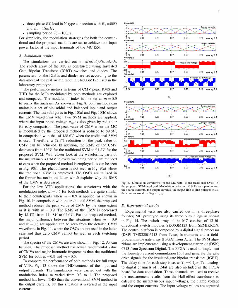
The performance metrics in terms of CMV peak, RMS andTHD for the MCs modulated by both methods are exploredand compared. The modulation index is first set as m= 0.9to verify the analysis. As shown in Fig. 8, both methods canmaintain a set of sinusoidal and balanced input and outputcurrents. The last subfigures in Fig. 10(a) and Fig. 10(b) showsthe CMV waveforms when two SVM methods are applied,where the input phase voltage vsa is also given by red colorfor easy comparison. The peak value of CMV when the MCis modulated by the proposed method is reduced to 89.8V ,in comparison with that of 155.6V when the traditional SVMis used. Therefore, a 42.3% reduction on the peak value ofCMV can be achieved. In addition, the RMS of the CMVdecreases from 156V for the traditional SVM to 61.5V for theproposed SVM. With closer look at the waveforms, parts ofthe instantaneous CMV in every switching period are reducedto zero when the proposed method is employed, as can be seenin Fig. 9(b). This phenomenon is not seen in Fig. 9(a) wherethe traditional SVM is employed. The OSCs are utilized inthe former but not in the latter, which explains why the RMSof the CMV is decreased.
For the low VTR applications, the waveforms with themodulation index m=0.5 for both methods are quite similarto their counterparts when m = 0.9 is applied, as shown inFig. 10. In comparison with the traditional SVM, the proposedmethod reduces the peak value of CMV by the same extentas it is with m = 0.9. The RMS of the CMV is decreasedby 45.4%, from 114.8V to 62.6V . For the proposed method,the major difference between the situations when m = 0.9and m= 0.5 are applied can be seen from the detailed CVMwaveforms in Fig. 11, where the OSCs are not used in the lattercase and thus zero CMV cannot be seen in each switchingperiod.
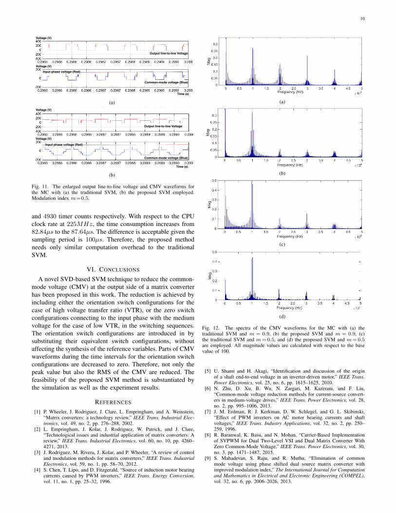
The spectra of the CMVs are also shown in Fig. 12. As canbe seen, The proposed method has lower fundamental valueof CMVs and major harmonic frequencies than the traditionalSVM for both m=0.9 and m=0.5.
To compare the performance of both methods for full rangeof VTR, Fig. 13 shows the THD contents of the input andoutput currents. The simulations were carried out with themodulation index m varied from 0.3 to 1. The proposedmethod has lower THD than the conventional SVM method inthe output currents, but this situation is reversed in the inputcurrents.
Voltage (V)
Time (s)
Voltage (V)
Time (s)
Time (s)
Time (s)
Current (A)
Current (A)
Source currents
Output currents
Output line Voltage
Common-mode Voltage
(a)
Voltage (V)
Time (s)
Voltage (V)
Time (s)
Time (s)
Time (s)
Current (A)
Current (A)
Source currents
Output currents
Output line Voltage
Common-mode Voltage
(b)
Fig. 8. Simulation waveforms for the MC with (a) the traditional SVM, (b)the proposed SVM employed. Modulation index m=0.9. From top to bottom:the source currents, the output currents, the output line-to-line voltages vAB ,the common-mode voltages vcm.
B. Experimental results
Experimental tests are also carried out in a three-phasefour-leg MC prototype using its three output legs as shownin Fig. 14. The switch array of the MC consists of 12 bi-directional switch modules SK60GM123 from SEMIKRON.The control platform is composed by a digital signal processor(DSP) TMS320C6713 from Texas Instruments and a field-programmable gate array (FPGA) from Actel. The SVM algo-rithms are implemented using a development starter kit (DSK)6713 from Spectrum Digital. The FPGA is used to implementthe four-step current commutation [56] and generate the gatedrive signals for the insulated-gate bipolar transistors (IGBT).The delay time for each step is set as Td=0.4µs. Ten analog-to digital channels of 12-bit are also included in the FPGAboard for data acquisition. These channels are used to receivethe measurement results from the Hall-effect transducers tocalculate the instantaneous input voltages, the clamp voltageand the output currents. The input voltage values are captured
9
Output line-to-line Voltage
Common-mode voltage (Blue)
Voltage (V)
Time (s)
Input phase voltage (Red)
Voltage (V)
(a)
Output line-to-line Voltage
Common-mode voltage (Blue)
Voltage (V)
Time (s)
Input phase voltage (Red)
Voltage (V)
(b)
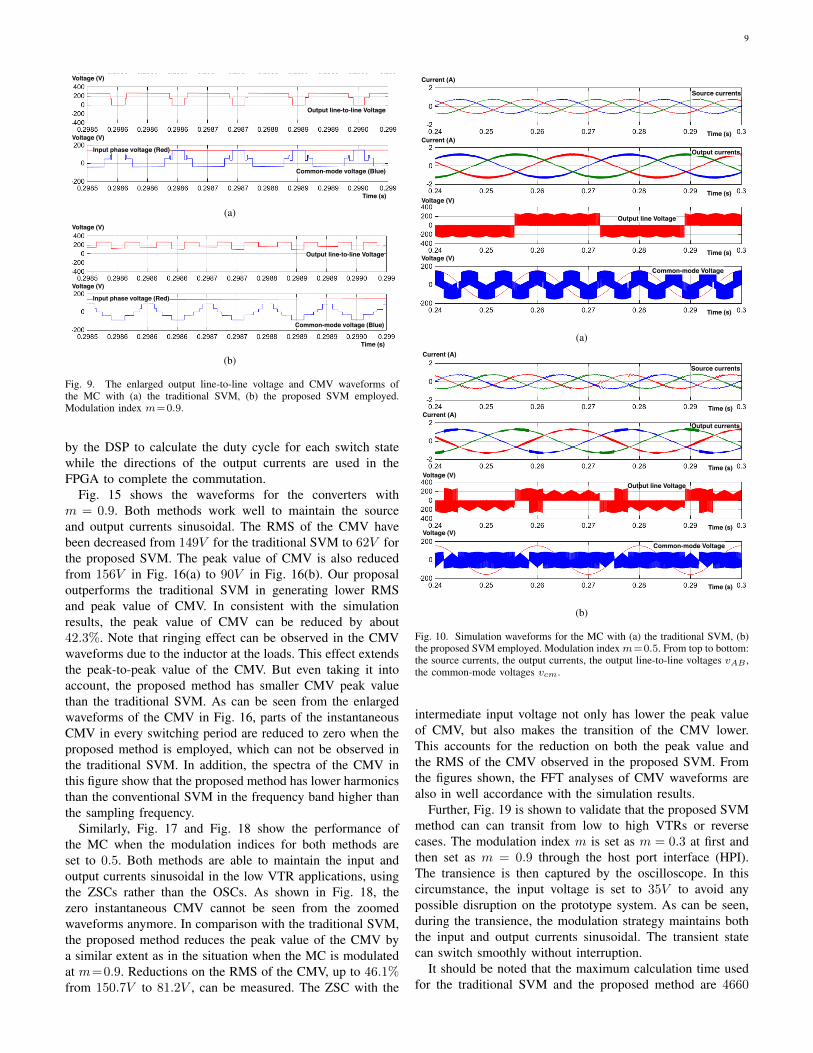
Fig. 9. The enlarged output line-to-line voltage and CMV waveforms ofthe MC with (a) the traditional SVM, (b) the proposed SVM employed.Modulation index m=0.9.
by the DSP to calculate the duty cycle for each switch statewhile the directions of the output currents are used in theFPGA to complete the commutation.
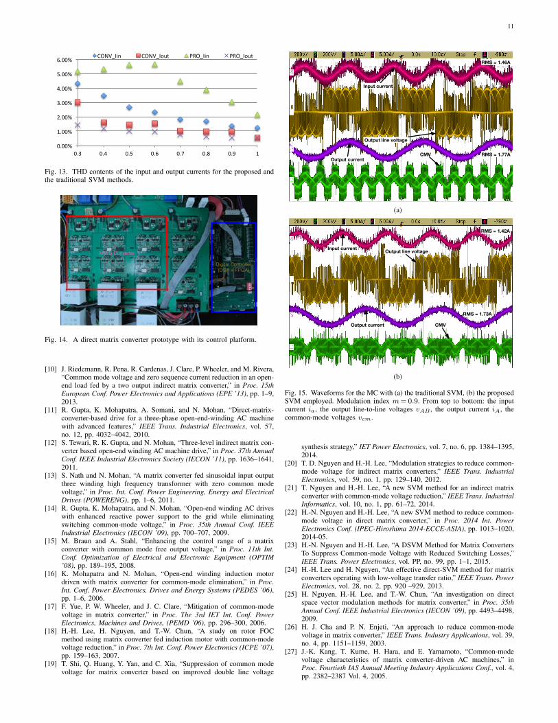
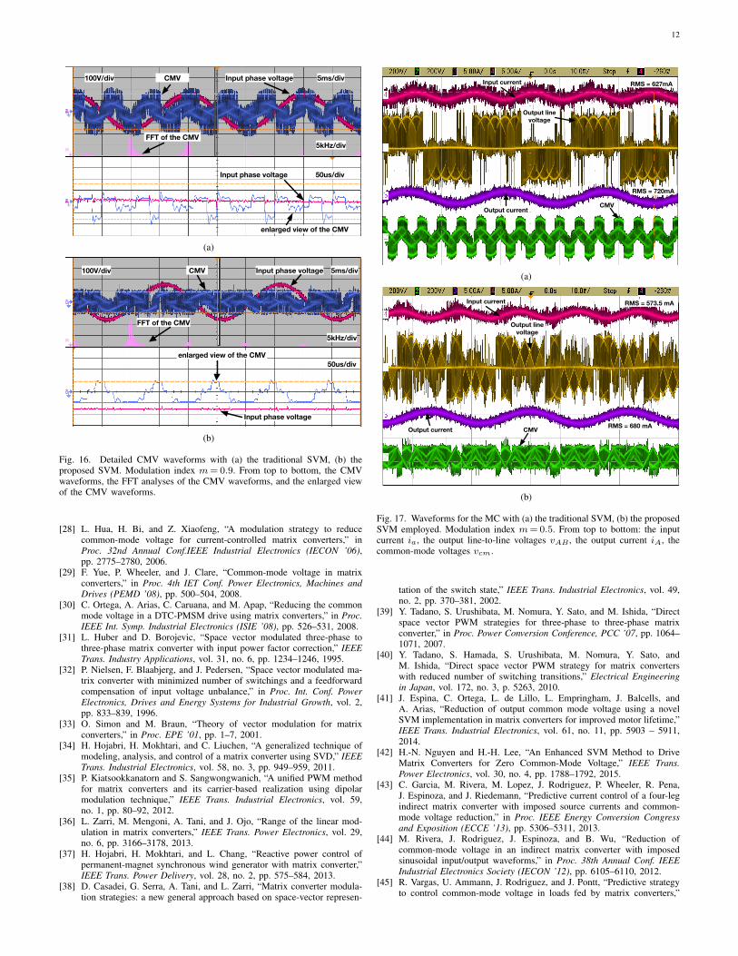
Fig. 15 shows the waveforms for the converters withm = 0.9. Both methods work well to maintain the sourceand output currents sinusoidal. The RMS of the CMV havebeen decreased from 149V for the traditional SVM to 62V forthe proposed SVM. The peak value of CMV is also reducedfrom 156V in Fig. 16(a) to 90V in Fig. 16(b). Our proposaloutperforms the traditional SVM in generating lower RMSand peak value of CMV. In consistent with the simulationresults, the peak value of CMV can be reduced by about42.3%. Note that ringing effect can be observed in the CMVwaveforms due to the inductor at the loads. This effect extendsthe peak-to-peak value of the CMV. But even taking it intoaccount, the proposed method has smaller CMV peak valuethan the traditional SVM. As can be seen from the enlargedwaveforms of the CMV in Fig. 16, parts of the instantaneousCMV in every switching period are reduced to zero when theproposed method is employed, which can not be observed inthe traditional SVM. In addition, the spectra of the CMV inthis figure show that the proposed method has lower harmonicsthan the conventional SVM in the frequency band higher thanthe sampling frequency.
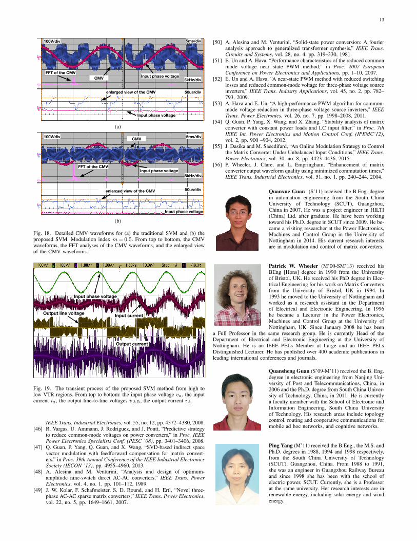
Similarly, Fig. 17 and Fig. 18 show the performance ofthe MC when the modulation indices for both methods areset to 0.5. Both methods are able to maintain the input andoutput currents sinusoidal in the low VTR applications, usingthe ZSCs rather than the OSCs. As shown in Fig. 18, thezero instantaneous CMV cannot be seen from the zoomedwaveforms anymore. In comparison with the traditional SVM,the proposed method reduces the peak value of the CMV bya similar extent as in the situation when the MC is modulatedat m=0.9. Reductions on the RMS of the CMV, up to 46.1%from 150.7V to 81.2V , can be measured. The ZSC with the
Voltage (V)
Time (s)
Voltage (V)
Time (s)
Time (s)
Time (s)
Current (A)
Current (A)
Source currents
Output currents
Output line Voltage
Common-mode Voltage
(a)
Voltage (V)
Time (s)
Voltage (V)
Time (s)
Time (s)
Time (s)
Current (A)
Current (A)
Source currents
Output currents
Output line Voltage
Common-mode Voltage
(b)
Fig. 10. Simulation waveforms for the MC with (a) the traditional SVM, (b)the proposed SVM employed. Modulation index m=0.5. From top to bottom:the source currents, the output currents, the output line-to-line voltages vAB ,the common-mode voltages vcm.
intermediate input voltage not only has lower the peak valueof CMV, but also makes the transition of the CMV lower.This accounts for the reduction on both the peak value andthe RMS of the CMV observed in the proposed SVM. Fromthe figures shown, the FFT analyses of CMV waveforms arealso in well accordance with the simulation results.
Further, Fig. 19 is shown to validate that the proposed SVMmethod can can transit from low to high VTRs or reversecases. The modulation index m is set as m = 0.3 at first andthen set as m = 0.9 through the host port interface (HPI).The transience is then captured by the oscilloscope. In thiscircumstance, the input voltage is set to 35V to avoid anypossible disruption on the prototype system. As can be seen,during the transience, the modulation strategy maintains boththe input and output currents sinusoidal. The transient statecan switch smoothly without interruption.
It should be noted that the maximum calculation time usedfor the traditional SVM and the proposed method are 4660
10
Output line-to-line Voltage
Common-mode voltage (Blue)
Voltage (V)
Time (s)
Input phase voltage (Red)Voltage (V)
(a)
Output line-to-line Voltage
Common-mode voltage (Blue)
Voltage (V)
Time (s)
Input phase voltage (Red)
Voltage (V)
(b)
Fig. 11. The enlarged output line-to-line voltage and CMV waveforms forthe MC with (a) the traditional SVM, (b) the proposed SVM employed.Modulation index m=0.5.
and 4930 timer counts respectively. With respect to the CPUclock rate at 225MHz, the time consumption increases from82.84µs to the 87.64µs. The difference is acceptable given thesampling period is 100µs. Therefore, the proposed methodneeds only similar computation overhead to the traditionalSVM.
VI. CONCLUSIONS
A novel SVD-based SVM technique to reduce the common-mode voltage (CMV) at the output side of a matrix converterhas been proposed in this work. The reduction is achieved byincluding either the orientation switch configurations for thecase of high voltage transfer ratio (VTR), or the zero switchconfigurations connecting to the input phase with the mediumvoltage for the case of low VTR, in the switching sequences.The orientation switch configurations are introduced in bysubstituting their equivalent switch configurations, withoutaffecting the synthesis of the reference variables. Parts of CMVwaveforms during the time intervals for the orientation switchconfigurations are decreased to zero. Therefore, not only thepeak value but also the RMS of the CMV are reduced. Thefeasibility of the proposed SVM method is substantiated bythe simulation as well as the experiment results.
REFERENCES
[1] P. Wheeler, J. Rodriguez, J. Clare, L. Empringham, and A. Weinstein,“Matrix converters: a technology review,” IEEE Trans. Industrial Elec-tronics, vol. 49, no. 2, pp. 276–288, 2002.
[2] L. Empringham, J. Kolar, J. Rodriguez, W. Patrick, and J. Clare,“Technological issues and industrial application of matrix converters: Areview,” IEEE Trans. Industrial Electronics, vol. 60, no. 10, pp. 4260–4271, 2013.
[3] J. Rodriguez, M. Rivera, J. Kolar, and P. Wheeler, “A review of controland modulation methods for matrix converters,” IEEE Trans. IndustrialElectronics, vol. 59, no. 1, pp. 58–70, 2012.
[4] S. Chen, T. Lipo, and D. Fitzgerald, “Source of induction motor bearingcurrents caused by PWM inverters,” IEEE Trans. Energy Conversion,vol. 11, no. 1, pp. 25–32, 1996.
(a)
(b)
(c)
(d)
Fig. 12. The spectra of the CMV waveforms for the MC with (a) thetraditional SVM and m = 0.9, (b) the proposed SVM and m = 0.9, (c)the traditional SVM and m=0.5, and (d) the proposed SVM and m=0.5are employed. All magnitude values are calculated with respect to the basevalue of 100.
[5] U. Shami and H. Akagi, “Identification and discussion of the originof a shaft end-to-end voltage in an inverter-driven motor,” IEEE Trans.Power Electronics, vol. 25, no. 6, pp. 1615–1625, 2010.
[6] N. Zhu, D. Xu, B. Wu, N. Zargari, M. Kazerani, and F. Liu,“Common-mode voltage reduction methods for current-source convert-ers in medium-voltage drives,” IEEE Trans. Power Electronics, vol. 28,no. 2, pp. 995–1006, 2013.
[7] J. M. Erdman, R. J. Kerkman, D. W. Schlegel, and G. L. Skibinski,“Effect of PWM inverters on AC motor bearing currents and shaftvoltages,” IEEE Trans. Industry Applications, vol. 32, no. 2, pp. 250–259, 1996.
[8] R. Baranwal, K. Basu, and N. Mohan, “Carrier-Based Implementationof SVPWM for Dual Two-Level VSI and Dual Matrix Converter WithZero Common-Mode Voltage,” IEEE Trans. Power Electronics, vol. 30,no. 3, pp. 1471–1487, 2015.
[9] S. Mahadevan, S. Raju, and R. Muthu, “Elimination of commonmode voltage using phase shifted dual source matrix converter withimproved modulation index,” The International Journal for Computationand Mathematics in Electrical and Electronic Engineering (COMPEL),vol. 32, no. 6, pp. 2006–2026, 2013.
11
0.00%$
1.00%$
2.00%$
3.00%$
4.00%$
5.00%$
6.00%$
0.3$ 0.4$ 0.5$ 0.6$ 0.7$ 0.8$ 0.9$ 1$
CONV_Iin$ CONV_Iout$ PRO_Iin$ PRO_Iout$
Fig. 13. THD contents of the input and output currents for the proposed andthe traditional SVM methods.
Matrix Converter
Digital Controller(DSP + FPGA)
Fig. 14. A direct matrix converter prototype with its control platform.
[10] J. Riedemann, R. Pena, R. Cardenas, J. Clare, P. Wheeler, and M. Rivera,“Common mode voltage and zero sequence current reduction in an open-end load fed by a two output indirect matrix converter,” in Proc. 15thEuropean Conf. Power Electronics and Applications (EPE ’13), pp. 1–9,2013.
[11] R. Gupta, K. Mohapatra, A. Somani, and N. Mohan, “Direct-matrix-converter-based drive for a three-phase open-end-winding AC machinewith advanced features,” IEEE Trans. Industrial Electronics, vol. 57,no. 12, pp. 4032–4042, 2010.
[12] S. Tewari, R. K. Gupta, and N. Mohan, “Three-level indirect matrix con-verter based open-end winding AC machine drive,” in Proc. 37th AnnualConf. IEEE Industrial Electronics Society (IECON ’11), pp. 1636–1641,2011.
[13] S. Nath and N. Mohan, “A matrix converter fed sinusoidal input outputthree winding high frequency transformer with zero common modevoltage,” in Proc. Int. Conf. Power Engineering, Energy and ElectricalDrives (POWERENG), pp. 1–6, 2011.
[14] R. Gupta, K. Mohapatra, and N. Mohan, “Open-end winding AC driveswith enhanced reactive power support to the grid while eliminatingswitching common-mode voltage,” in Proc. 35th Annual Conf. IEEEIndustrial Electronics (IECON ’09), pp. 700–707, 2009.
[15] M. Braun and A. Stahl, “Enhancing the control range of a matrixconverter with common mode free output voltage,” in Proc. 11th Int.Conf. Optimization of Electrical and Electronic Equipment (OPTIM’08), pp. 189–195, 2008.
[16] K. Mohapatra and N. Mohan, “Open-end winding induction motordriven with matrix converter for common-mode elimination,” in Proc.Int. Conf. Power Electronics, Drives and Energy Systems (PEDES ’06),pp. 1–6, 2006.
[17] F. Yue, P. W. Wheeler, and J. C. Clare, “Mitigation of common-modevoltage in matrix converter,” in Proc. The 3rd IET Int. Conf. PowerElectronics, Machines and Drives, (PEMD ’06), pp. 296–300, 2006.
[18] H.-H. Lee, H. Nguyen, and T.-W. Chun, “A study on rotor FOCmethod using matrix converter fed induction motor with common-modevoltage reduction,” in Proc. 7th Int. Conf. Power Electronics (ICPE ’07),pp. 159–163, 2007.
[19] T. Shi, Q. Huang, Y. Yan, and C. Xia, “Suppression of common modevoltage for matrix converter based on improved double line voltage
Input current
CMVOutput current
Output line voltage
RMS = 1.46A
RMS = 1.77A
(a)
Input current
CMVOutput current
Output line voltage
RMS = 1.42A
RMS = 1.73A
(b)
Fig. 15. Waveforms for the MC with (a) the traditional SVM, (b) the proposedSVM employed. Modulation index m=0.9. From top to bottom: the inputcurrent ia, the output line-to-line voltages vAB , the output current iA, thecommon-mode voltages vcm.
synthesis strategy,” IET Power Electronics, vol. 7, no. 6, pp. 1384–1395,2014.
[20] T. D. Nguyen and H.-H. Lee, “Modulation strategies to reduce common-mode voltage for indirect matrix converters,” IEEE Trans. IndustrialElectronics, vol. 59, no. 1, pp. 129–140, 2012.
[21] T. Nguyen and H.-H. Lee, “A new SVM method for an indirect matrixconverter with common-mode voltage reduction,” IEEE Trans. IndustrialInformatics, vol. 10, no. 1, pp. 61–72, 2014.
[22] H.-N. Nguyen and H.-H. Lee, “A new SVM method to reduce common-mode voltage in direct matrix converter,” in Proc. 2014 Int. PowerElectronics Conf. (IPEC-Hiroshima 2014-ECCE-ASIA), pp. 1013–1020,2014-05.
[23] H.-N. Nguyen and H.-H. Lee, “A DSVM Method for Matrix ConvertersTo Suppress Common-mode Voltage with Reduced Switching Losses,”IEEE Trans. Power Electronics, vol. PP, no. 99, pp. 1–1, 2015.
[24] H.-H. Lee and H. Nguyen, “An effective direct-SVM method for matrixconverters operating with low-voltage transfer ratio,” IEEE Trans. PowerElectronics, vol. 28, no. 2, pp. 920 –929, 2013.
[25] H. Nguyen, H.-H. Lee, and T.-W. Chun, “An investigation on directspace vector modulation methods for matrix converter,” in Proc. 35thAnnual Conf. IEEE Industrial Electronics (IECON ’09), pp. 4493–4498,2009.
[26] H. J. Cha and P. N. Enjeti, “An approach to reduce common-modevoltage in matrix converter,” IEEE Trans. Industry Applications, vol. 39,no. 4, pp. 1151–1159, 2003.
[27] J.-K. Kang, T. Kume, H. Hara, and E. Yamamoto, “Common-modevoltage characteristics of matrix converter-driven AC machines,” inProc. Fourtieth IAS Annual Meeting Industry Applications Conf., vol. 4,pp. 2382–2387 Vol. 4, 2005.
12
Input phase voltage100V/div
FFT of the CMV
enlarged view of the CMV
5ms/div
50us/div
5kHz/div
Input phase voltage
CMV
(a)
CMV Input phase voltage100V/div
FFT of the CMV
enlarged view of the CMV
5ms/div
50us/div
5kHz/div
Input phase voltage
(b)
Fig. 16. Detailed CMV waveforms with (a) the traditional SVM, (b) theproposed SVM. Modulation index m= 0.9. From top to bottom, the CMVwaveforms, the FFT analyses of the CMV waveforms, and the enlarged viewof the CMV waveforms.
[28] L. Hua, H. Bi, and Z. Xiaofeng, “A modulation strategy to reducecommon-mode voltage for current-controlled matrix converters,” inProc. 32nd Annual Conf.IEEE Industrial Electronics (IECON ’06),pp. 2775–2780, 2006.
[29] F. Yue, P. Wheeler, and J. Clare, “Common-mode voltage in matrixconverters,” in Proc. 4th IET Conf. Power Electronics, Machines andDrives (PEMD ’08), pp. 500–504, 2008.
[30] C. Ortega, A. Arias, C. Caruana, and M. Apap, “Reducing the commonmode voltage in a DTC-PMSM drive using matrix converters,” in Proc.IEEE Int. Symp. Industrial Electronics (ISIE ’08), pp. 526–531, 2008.
[31] L. Huber and D. Borojevic, “Space vector modulated three-phase tothree-phase matrix converter with input power factor correction,” IEEETrans. Industry Applications, vol. 31, no. 6, pp. 1234–1246, 1995.
[32] P. Nielsen, F. Blaabjerg, and J. Pedersen, “Space vector modulated ma-trix converter with minimized number of switchings and a feedforwardcompensation of input voltage unbalance,” in Proc. Int. Conf. PowerElectronics, Drives and Energy Systems for Industrial Growth, vol. 2,pp. 833–839, 1996.
[33] O. Simon and M. Braun, “Theory of vector modulation for matrixconverters,” in Proc. EPE ’01, pp. 1–7, 2001.
[34] H. Hojabri, H. Mokhtari, and C. Liuchen, “A generalized technique ofmodeling, analysis, and control of a matrix converter using SVD,” IEEETrans. Industrial Electronics, vol. 58, no. 3, pp. 949–959, 2011.
[35] P. Kiatsookkanatorn and S. Sangwongwanich, “A unified PWM methodfor matrix converters and its carrier-based realization using dipolarmodulation technique,” IEEE Trans. Industrial Electronics, vol. 59,no. 1, pp. 80–92, 2012.
[36] L. Zarri, M. Mengoni, A. Tani, and J. Ojo, “Range of the linear mod-ulation in matrix converters,” IEEE Trans. Power Electronics, vol. 29,no. 6, pp. 3166–3178, 2013.
[37] H. Hojabri, H. Mokhtari, and L. Chang, “Reactive power control ofpermanent-magnet synchronous wind generator with matrix converter,”IEEE Trans. Power Delivery, vol. 28, no. 2, pp. 575–584, 2013.
[38] D. Casadei, G. Serra, A. Tani, and L. Zarri, “Matrix converter modula-tion strategies: a new general approach based on space-vector represen-
Input current
CMVOutput current
Output line voltage
RMS = 627mA
RMS = 720mA
(a)
Input current
CMVOutput current
Output line voltage
RMS = 573.5 mA
RMS = 680 mA
(b)
Fig. 17. Waveforms for the MC with (a) the traditional SVM, (b) the proposedSVM employed. Modulation index m=0.5. From top to bottom: the inputcurrent ia, the output line-to-line voltages vAB , the output current iA, thecommon-mode voltages vcm.
tation of the switch state,” IEEE Trans. Industrial Electronics, vol. 49,no. 2, pp. 370–381, 2002.
[39] Y. Tadano, S. Urushibata, M. Nomura, Y. Sato, and M. Ishida, “Directspace vector PWM strategies for three-phase to three-phase matrixconverter,” in Proc. Power Conversion Conference, PCC ’07, pp. 1064–1071, 2007.
[40] Y. Tadano, S. Hamada, S. Urushibata, M. Nomura, Y. Sato, andM. Ishida, “Direct space vector PWM strategy for matrix converterswith reduced number of switching transitions,” Electrical Engineeringin Japan, vol. 172, no. 3, p. 5263, 2010.
[41] J. Espina, C. Ortega, L. de Lillo, L. Empringham, J. Balcells, andA. Arias, “Reduction of output common mode voltage using a novelSVM implementation in matrix converters for improved motor lifetime,”IEEE Trans. Industrial Electronics, vol. 61, no. 11, pp. 5903 – 5911,2014.
[42] H.-N. Nguyen and H.-H. Lee, “An Enhanced SVM Method to DriveMatrix Converters for Zero Common-Mode Voltage,” IEEE Trans.Power Electronics, vol. 30, no. 4, pp. 1788–1792, 2015.
[43] C. Garcia, M. Rivera, M. Lopez, J. Rodriguez, P. Wheeler, R. Pena,J. Espinoza, and J. Riedemann, “Predictive current control of a four-legindirect matrix converter with imposed source currents and common-mode voltage reduction,” in Proc. IEEE Energy Conversion Congressand Exposition (ECCE ’13), pp. 5306–5311, 2013.
[44] M. Rivera, J. Rodriguez, J. Espinoza, and B. Wu, “Reduction ofcommon-mode voltage in an indirect matrix converter with imposedsinusoidal input/output waveforms,” in Proc. 38th Annual Conf. IEEEIndustrial Electronics Society (IECON ’12), pp. 6105–6110, 2012.
[45] R. Vargas, U. Ammann, J. Rodriguez, and J. Pontt, “Predictive strategyto control common-mode voltage in loads fed by matrix converters,”
13
CMV Input phase voltage
100V/div
FFT of the CMV
enlarged view of the CMV
5ms/div
50us/div
5kHz/div
Input phase voltage
(a)
CMV
Input phase voltage
100V/div
FFT of the CMV
enlarged view of the CMV
5ms/div
50us/div
5kHz/div
Input phase voltage
(b)
Fig. 18. Detailed CMV waveforms for (a) the traditional SVM and (b) theproposed SVM. Modulation index m= 0.5. From top to bottom, the CMVwaveforms, the FFT analyses of the CMV waveforms, and the enlarged viewof the CMV waveforms.
Input phase voltage
Output current
Input currentOutput line voltage
Fig. 19. The transient process of the proposed SVM method from high tolow VTR regions. From top to bottom: the input phase voltage va, the inputcurrent ia, the output line-to-line voltages vAB , the output current iA.
IEEE Trans. Industrial Electronics, vol. 55, no. 12, pp. 4372–4380, 2008.[46] R. Vargas, U. Ammann, J. Rodriguez, and J. Pontt, “Predictive strategy
to reduce common-mode voltages on power converters,” in Proc. IEEEPower Electronics Specialists Conf. (PESC ’08), pp. 3401–3406, 2008.
[47] Q. Guan, P. Yang, Q. Guan, and X. Wang, “SVD-based indirect spacevector modulation with feedforward compensation for matrix convert-ers,” in Proc. 39th Annual Conference of the IEEE Industrial ElectronicsSociety (IECON ’13), pp. 4955–4960, 2013.
[48] A. Alesina and M. Venturini, “Analysis and design of optimum-amplitude nine-switch direct AC-AC converters,” IEEE Trans. PowerElectronics, vol. 4, no. 1, pp. 101–112, 1989.
[49] J. W. Kolar, F. Schafmeister, S. D. Round, and H. Ertl, “Novel three-phase AC-AC sparse matrix converters,” IEEE Trans. Power Electronics,vol. 22, no. 5, pp. 1649–1661, 2007.
[50] A. Alesina and M. Venturini, “Solid-state power conversion: A fourieranalysis approach to generalized transformer synthesis,” IEEE Trans.Circuits and Systems, vol. 28, no. 4, pp. 319–330, 1981.
[51] E. Un and A. Hava, “Performance characteristics of the reduced commonmode voltage near state PWM method,” in Proc. 2007 EuropeanConference on Power Electronics and Applications, pp. 1–10, 2007.
[52] E. Un and A. Hava, “A near-state PWM method with reduced switchinglosses and reduced common-mode voltage for three-phase voltage sourceinverters,” IEEE Trans. Industry Applications, vol. 45, no. 2, pp. 782–793, 2009.
[53] A. Hava and E. Un, “A high-performance PWM algorithm for common-mode voltage reduction in three-phase voltage source inverters,” IEEETrans. Power Electronics, vol. 26, no. 7, pp. 1998–2008, 2011.
[54] Q. Guan, P. Yang, X. Wang, and X. Zhang, “Stability analysis of matrixconverter with constant power loads and LC input filter,” in Proc. 7thIEEE Int. Power Electronics and Motion Control Conf. (IPEMC’12),vol. 2, pp. 900 –904, 2012.
[55] J. Dasika and M. Saeedifard, “An Online Modulation Strategy to Controlthe Matrix Converter Under Unbalanced Input Conditions,” IEEE Trans.Power Electronics, vol. 30, no. 8, pp. 4423–4436, 2015.
[56] P. Wheeler, J. Clare, and L. Empringham, “Enhancement of matrixconverter output waveform quality using minimized commutation times,”IEEE Trans. Industrial Electronics, vol. 51, no. 1, pp. 240–244, 2004.
Quanxue Guan (S’11) received the B.Eng. degreein automation engineering from the South ChinaUniversity of Technology (SCUT), Guangzhou,China in 2007. He was a project engineer in HILTI(China) Ltd. after graduate. He have been workingtoward his Ph.D. degree in SCUT since 2009. He be-came a visiting researcher at the Power Electronics,Machines and Control Group in the University ofNottingham in 2014. His current research interestsare in modulation and control of matrix converters.
Patrick W. Wheeler (M’00-SM’13) received hisBEng [Hons] degree in 1990 from the Universityof Bristol, UK. He received his PhD degree in Elec-trical Engineering for his work on Matrix Convertersfrom the University of Bristol, UK in 1994. In1993 he moved to the University of Nottingham andworked as a research assistant in the Departmentof Electrical and Electronic Engineering. In 1996he became a Lecturer in the Power Electronics,Machines and Control Group at the University ofNottingham, UK. Since January 2008 he has been
a Full Professor in the same research group. He is currently Head of theDepartment of Electrical and Electronic Engineering at the University ofNottingham. He is an IEEE PELs Member at Large and an IEEE PELsDistinguished Lecturer. He has published over 400 academic publications inleading international conferences and journals.
Quansheng Guan (S’09-M’11) received the B. Eng.degree in electronic engineering from Nanjing Uni-versity of Post and Telecommunications, China, in2006 and the Ph.D. degree from South China Univer-sity of Technology, China, in 2011. He is currentlya faculty member with the School of Electronic andInformation Engineering, South China Universityof Technology. His research areas include topologycontrol, routing and cooperative communications formobile ad hoc networks, and cognitive networks.
Ping Yang (M’11) received the B.Eng., the M.S. andPh.D. degrees in 1988, 1994 and 1998 respectively,from the South China University of Technology(SCUT), Guangzhou, China. From 1988 to 1991,she was an engineer in Guangzhou Railway Bureauand since 1998 she has been with the school ofelectric power, SCUT. Currently, she is a Professorat the same university. Her research interests are inrenewable energy, including solar energy and windenergy.