Embed Size (px)
Citation preview
commodoresemiconductor group
MOS TECHNOLOGY, INC.950 Rittenhouse Rd., Norristown, PA 19403 ■ Tel.: 215/666-7950 ■ TLX 846-100 MOSTECHGY VAFG
65245 OCTAL BUS TRANSCEIVER WITH 3-STATE OUTPUTS
DESCRIPTION
The 65245 is an octal bus transceiver designed for asynchronous, bi-directional communication between data busses.
The level of the Directiomnput (DIR) allows data transmission from bus A to bus B or from bus B to bus A. The Enable input (E) can be used to provide isolation between the busses.
The device is fully TTL and CMOS compatible, and is pin-for-pin compatible with the 74LS245.
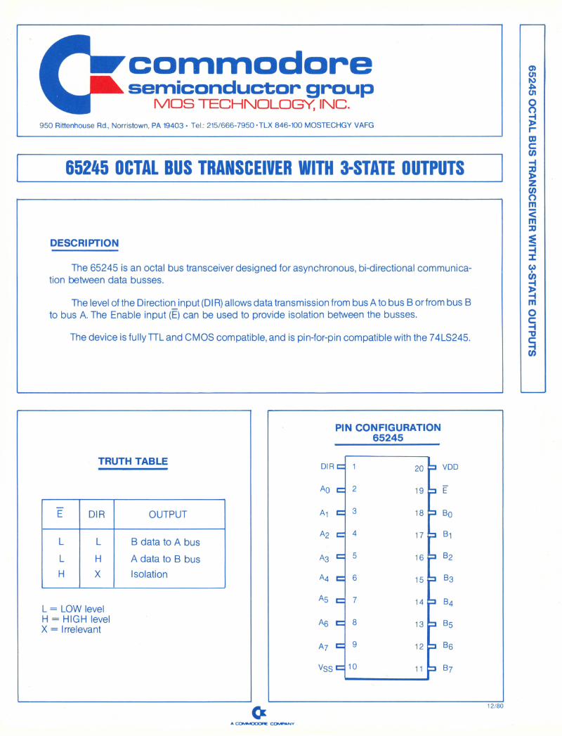
TRUTH TABLE
E DIR OUTPUT
L L B data to A bus
L H A data to B busH X Isolation
L = LOW level H = HIGH level X = Irrelevant
PIN CONFIGURATION65245
DIR C 1 20 D VDD
Ao E 2 19 D E
Ai e= 3 18 0DQ
_n
_
A2 c r 4 17 3 Eh
A3 = 5 16 □ B2
A4 e 6 15 3 B3
A5 ^ 7 14 3 B4
A6 C= 8 13 3 B5
a? e= 9 12 3 B6
Vss = 1011.
12/80
A COM M OOOR6 COM PANY
65245 OCTAL
BUS TRANSCEIVER
WITH
3-STATE O
UTPU
TS

This device contains circuitry to protect the inputs against damage due to high static voltages, however, it is advised that normal precautions be taken to avoid application of any voltage higher than maximum rated voltages to this circuit.
ELECTRICAL CHARACTERISTICS (Vcc = 5.0V ± 5%, Vss = 0, Ta =0° to + 70 C)
CHARACTERISTIC SYMBOL MIN. TYP. MAX. UNIT
Input High Voltage VIH 2.0 - - Vdc
Input Low Voltage VIL — — 0.8 Vdc
Output High VoltageVcc=M 1N, VI H=2.0V IOH= -3m A VOH 2.4 Vdc
IOH= —15mA 2.0 - -
Output Low VoltageVcc=MIN, VIL = 0.8V IO L= 12mA VOL 0.4 Vdc
IOL = 24mA - 0.5
High-lmpedance Output Current E = 2.0V, Vcc = MAXVout = 2-7V
IOZH - - 50 f j A
High-lmpedance Output Current E* = 2.0V, Vcc = MAX Vout = 0.4V
IOZL - - -5 0 yuA
High-Level Input Current Vcc=MAX, VIH = 2 .7V 11H — 20 100 nA
Low-Level Input CurrentVcc = MAX, VI L = 0.4V ML — 20 -100 nA
High-Level Output Current Vcc=NOM, Vout = 2.4V IOH — — -1 5 mA
Low-Level Output Current Vcc = NOM, Vout = 0.4V IOL - - 24 mA
Power Supply Current Outputs High Outputs Low Outputs Hi-Z ICC —
474456
46100105 mA
MAXIMUM RATINGS
RATING SYMBOL VALUE UNIT
SUPPLY VOLTAGE Vcc -0.3 to +7.0 Vdc
INPUT VOLTAGE Vin -0 .3 to +7.0 Vdc
OPERATING TEMPERATURE ta 0 to +70 °C
STORAGE TEMPERATURE tstg -5 5 to +150 °C
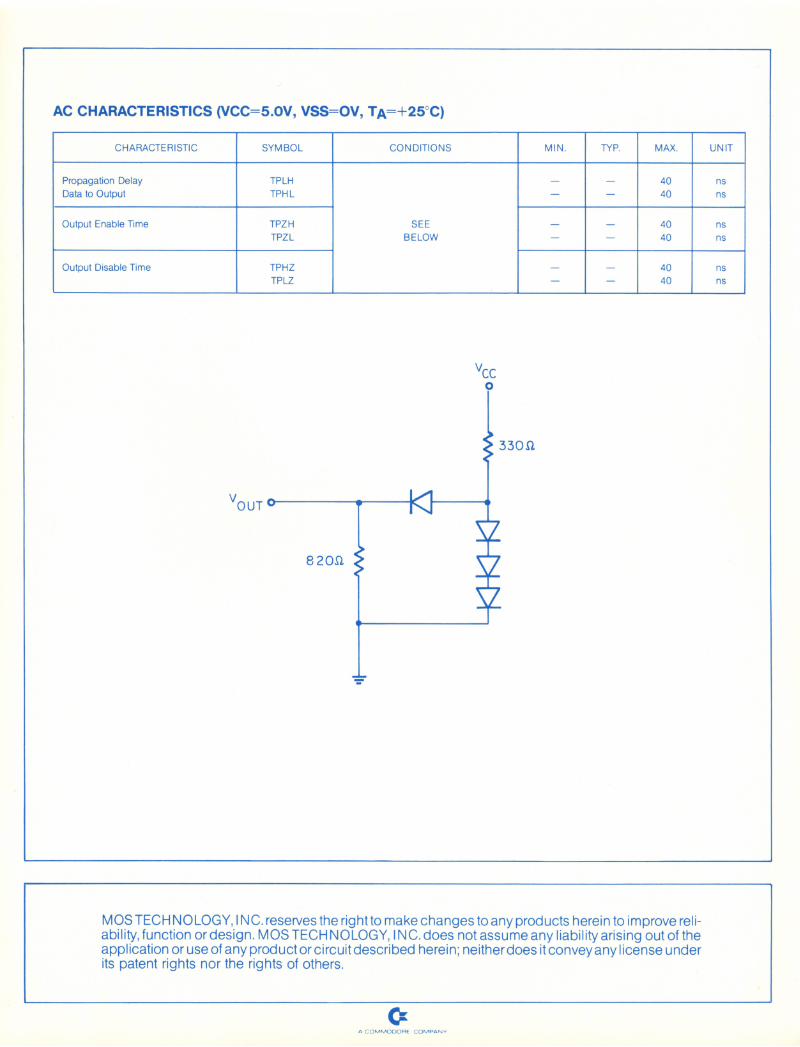
AC CHARACTERISTICS (VCC=5.0V, VSS=OV, Ta=+25°C)
CHARACTERISTIC SYMBOL CONDITIONS MIN. TYP. MAX. UNIT
Propagation Delay TPLH _ _ 40 nsData to Output TPHL — — 40 ns
Output Enable Time TPZH SEE _ _ 40 nsTPZL BELOW — — 40 ns
Output Disable Time TPHZ _ _ 40 nsTPLZ — — 40 ns
MOS TECHNOLOGY, INC. reserves the rightto make changes to any products herein to improve reliability, function or design. MOS TECHNOLOGY, INC. does not assume any liability arising out of the application or use of any product or circuit described herein; neither does it convey any license under its patent rights nor the rights of others.
CrA C O M M O D O R E C O M P A N Y