Embed Size (px)
Citation preview

1
COMMISSION D: Electronics and Photonics
(November 2010 - October 2013)
Edited by Tadao Nagatsuma, Osaka University
Electronics and Photonics cover huge scientific and technological fields. Among them, in this
report, we have selected several important topical areas, where in particular Japanese leading
researchers have actively contributed between 2010 and 2013. They overviewed recent
remarkable advances in their specialized areas.
The following is a list of areas that the chapter editor has taken up.
D1. Metamaterials
E. Sano
Hokkaido University
D2. Mid-infrared Quantum Cascade Lasers and Antennas
K. Kasahara
Ritsumeikan University
D3. THz Parametric Amplifier
K. Kawase
Nagaya University
D4. Broadband Continuous THz Wave Emitters and Detectors
H. Ito
Kitasato University
D5. Plasmonic Device Technology for Emission and Detection of Terahertz Radiation
T. Otsuji
Tohoku University
D6. Photonic Microstructures for Silicon Photonics Applications
M. Fujita
Osaka University

2
D7. Microwave Multiplexers for Readout of Superconducting Detector Array
S. Kohjiro
National Institute of Advanced Industrial Science and Technology
D8. High Capacity Optical Fiber Transmission Systems
H. Toda
Doshisha University
D9. Small Cell Configurations using RoF Entrance Network Technologies
K. Tsukamoto
Osaka Institute of Technology
D10. Convergence of Wireless and Wired Technologies towards Next Generation
Access Networks
K. Iwatsuki
Tohoku University
D11. Optical Access Technologies for Mobile Fronthaul
J. Kani
NTT
D1. Metamaterials
Eiichi Sano
Hokkaido University
Recent years have seen the development of wireless sensor networks (WSNs) to realize
ubiquitous computing environments. A WSN is a network to get information from wireless sensor
nodes located at distant sites. Today, WSNs are used in various fields such as building and
apartment security and healthcare monitoring. Small size and low power consumption is needed
for wireless sensor nodes to be deployed and to ensure maintenance-free operation in various
environments since it is difficult to constantly maintain a huge number of sensor nodes in a
manner like that of replacing batteries [1].
The size of a wireless sensor node is mainly determined by antenna size. In recent years,
several extensive attempts have been made to fabricate electrically small antennas for system-on-
3
a-chip (SoC) or system-in-a-package (SiP) application [2], [3]. However, in such antennas the
antenna gain is constrained to the Harrington limit, while the impedance matching and directivity
characteristics deteriorate. Various methods for reducing antenna size have been reported [3-8].
Using a dipole antenna loaded with a left-handed ladder structure is a promising technique for
reducing the size of antennas [5]. When parallel plate capacitors and spiral inductors are fabricated
on a printed circuit board (PCB) with a thickness of a few mm, however, the sizes of the capacitors
and the widths of the spiral inductors are expected to be more than 4 × 4 mm and 2 mm for
achieving left-handed components operating at 2.4 GHz, and these components cannot reduce the
antenna size to less than a conventional dipole antenna. In contrast, lumped components of
inductors and capacitors with sizes of 0.4 × 0.2 and 0.6 × 0.3 mm are commercially available.
In this report, the left-handed dipole antenna with the right/left-handed ladder structure was
designed and fabricated using lumped inductors and capacitors.
The length for a standard half-wavelength dipole antenna operating at 2.4 GHz is about 6 cm,
which is too long to achieve a small-size sensor node. On the other hand, we encounter a problem
that the antenna gain degrades as the antenna size is reduced. The highest achievable gain of an
electrically small antenna that can be enclosed within a sphere of effective radius r is given by
G=(kr)2+2kr (1)
where k is the wave number. The highest gain for small antennas operating at 2.45 GHz is
calculated to be 1.0 dBi with an antenna length of 20 mm corresponding to 0.160 and kr = 0.502
(0: free space wavelength).
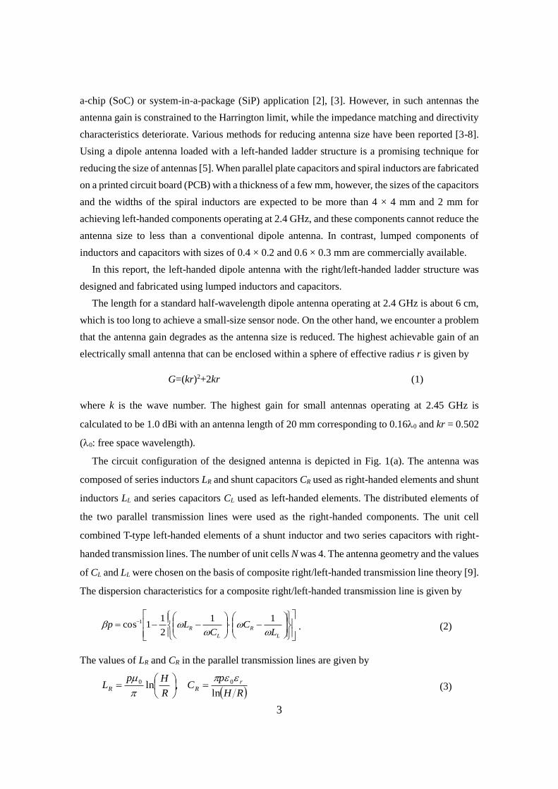
The circuit configuration of the designed antenna is depicted in Fig. 1(a). The antenna was
composed of series inductors LR and shunt capacitors CR used as right-handed elements and shunt
inductors LL and series capacitors CL used as left-handed elements. The distributed elements of
the two parallel transmission lines were used as the right-handed components. The unit cell
combined T-type left-handed elements of a shunt inductor and two series capacitors with right-
handed transmission lines. The number of unit cells N was 4. The antenna geometry and the values
of CL and LL were chosen on the basis of composite right/left-handed transmission line theory [9].
The dispersion characteristics for a composite right/left-handed transmission line is given by
L
R
L
RL
CC
Lp
11
2
11cos 1
. (2)
The values of LR and CR in the parallel transmission lines are given by
RH
pC
R
HpL r
RRln
,ln 00
(3)

4
where H is the distance between the two parallel lines and R is the half line width [6]. Since both
ends of the lines are open, the phase difference between the two open ends must be at the
operating frequency. This means that p must equal /4 at the target frequency of 2.4 GHz. The
designed values were: the unit cell size = 5 mm, H = 2 mm, R = 0.15 mm, CL = 0.5 pF, and LL =
3.9 nH. The antenna was simulated with a finite-difference time-domain (FDTD) electromagnetic
simulator (EMpro, Agilent).
A T-junction balun was designed for the differential signal input to the dipole antenna. The
balun was composed of a high-pass filter (HPF), a low-pass filter (LPF), and a T-junction [Fig.
1(b)]. Fifth-order LC circuits were used for the HPF and LPF, which shifted the signal by +90° in
the leading phase and -90° in the lagging phase, respectively. Each element of the balun was
simulated with a circuit simulator (ADS). Finally, the impedance matching was simulated for the
left-handed antenna combined with the T-junction balun.
The antenna with balun was constructed on FR4 substrate with a thickness of 1.6 mm.
Commercially available chip capacitors and inductors with a size of 0.6 × 0.3 mm were used. Fig.
1b shows a photograph of the fabricated antenna with balun. To eliminate the effect of variation
in the lumped elements, we fabricated four antennas and averaged the measured characteristics.
(a) (b)
Fig. 1. Configuration of left-handed dipole antenna with balun and photograph of fabricated antenna
with balun. (a) Circuit configuration. (b) Photograph.
The fabricated antennas were measured using a standard dipole antenna with a gain of 2.14 dB
and a vector network analyser (VNA). Port 1 of the VNA was connected to one of the fabricated
antennas, and Port 2 of the VNA was connected to the dipole antenna. The gain was calibrated
with the gain measured between two standard dipole antennas.
Fig. 2(a) shows the measured return losses for each antenna. An impedance matching of less
than -10 dB was obtained in the frequency band from 2.4 to 2.5 GHz. The matching between
designed and measured return losses was quite good. Fig. 2(b) shows the actual gain for the
BalunUnit cell
~Feed point
L
p
H
Capacitor
Inductor
HPF
LPF
Port 1
Port 2
Port 3
(q:+90)
(q:-90)
Difference
signal
(180°)
20 mm

5
antenna. The measured antenna gain was -0.01 dBi. The simulated antenna gain (-0.66 dBi) was
slightly lower than the measured gain. The difference might have been caused by the variation in
the lumped elements and the effect of the solder used to mount the components. Fig. 3 compares
measured and simulated directivities. The directivity of the fabricated antenna was measured by
changing the angle/theta from 0 to 90 degrees by 5 degree steps in the E-plane. A fairly good
agreement was obtained for all degree steps. Fig. 4 compares the antenna gains achieved in this
work with those reported in previous literature [3]-[5], [7], [8]. Their measurement values are the
highest gain ever achieved for the antennas at the same kr operating at 2.45 GHz.
(a) (b)
Fig. 2. Return loss and actual gain. (a) Measured and simulated return losses. (b) Measured actual
gain.
Fig. 3. Comparisons between measured and simulated directivity in E-plane.
-30
-25
-20
-15
-10
-5
0
5
1.5 2 2.5 3 3.5
MeasurementSimulation
Retu
rn loss
(dB
)
Freqency (GHz)
-50
-40
-30
-20
-10
0
2 2.2 2.4 2.6 2.8 3
Acu
tual
gai
n (
dB)
Frequency (GHz)
-20
-15
-10
-5
00
30
60
90
120
150180
210
240
270
300
330
MeasurementSimulation
Act
ual ga
in (dB
)
Theta (deg)
f=2.45 GHz

6
Fig. 4. Comparison of fabricated antenna gain with those reported in literature [3]-[5], [7], [8].
On the basis of the composite right/left-handed transmission line theory, we designed the left-
handed antenna with the lumped components to reduce the antenna size. The actual gain of the
fabricated antenna was -0.01 dBi, which was about 1 dB lower than the Harrington limit and the
highest ever achieved for fabricated antennas operating at around 2.45 GHz (kr = 0.502).
References
[1] K. Takahagi, H. Matsushita, T. Iida, M. Ikebe, Y. Amemiya, and E. Sano, “Low-power wake-
up receiver with subthreshold CMOS circuits for wireless sensor networks,” Analog Integrated
Circuits and Signal Processing, vol. 75, pp. 199-205, 2013.
[2] K. Takahagi and E. Sano, “High-gain silicon on-chip antenna with artificial dielectric layer,”
IEEE Trans. Antennas Propag., vol. 59, no. 10, pp. 3624-3629, 2011.
[3] P. L. Chi, R. Waterhouse, and T. Itoh, “Antenna miniaturization using slow wave enhancement
factor from loaded transmission line models,” IEEE Trans. Antennas Propag., vol. 59, no. 1, pp.
48-57, 2011.
[4] M. C. Scardelletti, G. E. Ponchak, S. Merritt, J. S. Minor, and C. A. Zorman, “Electrically
small folded slot antenna utilizing capacitive loaded slot lines,” IEEE Radio Wireless Symp.,
Orlando FL, USA, Jan. 2008, pp. 731-734.
[5] Q. Liu, P. S. Hall, and A. L. Borja, “Efficiency of electrically small dipole antennas loaded
with left-handed transmission line,” IEEE Trans. Antennas Propag., vol. 57, no. 10, pp. 3009-
3017, 2009.
[6] S. Kamada, N. Michishita, and Y. Yamada, “Short-length leaky wave antenna using composite
right/left-handed ladder network for UHF band,” Int. Workshop on Antenna Technology (iWAT),
March 2010, pp. 1-4.
-25
-20
-15
-10
-5
0
5
10
0 0.2 0.4 0.6 0.8 1 1.2 1.4
MeasurementSimulationHarrington limitReported gain
Gai
n (d
B)
kr

7
[7] M. A. Antoniades and G. V. Eleftheriades, “A folded-monopole model for electrically small
NRI-TL metamaterial antennas,” IEEE Antennas Wireless Propag. Lett., vol. 7, pp. 425-428, 2008.
[8] K. V. Caekenberghe, N. Behdad, K. M. Brakora, and K. Sarabandi, “A 2.45-GHz electrically
small slot antenna,” IEEE Antennas Wireless Propag. Lett., vol. 7, pp. 346-348, 2008.
[9] C. C. Caloz, A. Sanada, and T. Itoh, “A novel composite right-/left-handed coupled-line
directional coupler with arbitrary coupling level and broad bandwidth,” IEEE Trans. Microwave
Theory Tech., vol. 52, no. 3, pp. 980-992, 2004.
D2. Mid-infrared Quantum Cascade Lasers and Antennas
K. Kasahara
Ritsumeikan University
Significant progress in mid-infrared distributed-feedback (DFB)-quantum cascade
lasers (QCLs) capable of continuous-wave (cw) operation above room temperature
has allowed for the monitoring of trace gases relating to environmental and energy
issues [1], [2]. Theoretical treatment for the relative intensity noise (RIN) of QCLs
and the laser power modulation due to the light returning from the detector at liquid-
nitrogen temperature, have been reported so far. However, there have been no
experimental reports discussing the RIN of DFB-QCLs, following the gained
knowledge of the linewidth enhancement factor, , and optical coupling efficiency.
Therefore, a new method using a movable reflection mirror was reported to obtain
both parameters experimentally (Fig. 1), where a commercially available 6.1 m
DFB-QCL with a cw threshold current of Ith = 461 mA at 253 K was used [3]. An Al-
coated reflection mirror mounted on a voice coil was placed at the end of one arm.
The other beam transmitted through the beam splitter was collected by another AR-
coated CaF2 lens, and focused onto a Peltier-cooled HgCdTe photovoltaic detector
(MCT-PV). After the RIN measurements were taken, the mirror was moved back and
forth by the voice coil to observe the self-mixing waveform, which was taken out
through a capacitor, to extract the feedback parameter, C, which is defined as
follows:
(1),1
212
nl
CereLC

8
where represents the coupling efficiency of returning light to a laser, Le is the
distance between a laser chip and an external mirror, re is amplitude reflectivity of
the reflection mirror, l is the cavity length (QCL: 2 mm), and n represents the
refractive index. 1C is a complex coefficient which depends only on solitary DFB
laser modal characteristics. Figure 2 shows the RIN as a function of a normalized
pumping current a (= I/Ith-1). There wasn’t any marked change in the RIN. The -
parameter and C of the QCL obtained from the self-mixing waveform were concluded
to be about -2.2 and 2.9. To estimate , one needs to know 1C shown in (1). C1 was 4.0
10 -1 < C1 < 7.7 10-1, and the respective coupling efficiencies calculated from (1)
was 2.0 10-2 < < 3.8 10-2. Therefore, the coupling efficiency was estimated to be
more than 2.0% at least. The estimated coupling efficiency of the light returning to
the QCL was at such a level that it would result in the coherent collapse if it were
DFB-lase diodes (LDs). However, the RIN was almost the same as that without
feedback.
Fig. 1. Experimental setup used for the RIN measurements of the DFB-QCL. Asymmetric
triangular voltage with an up and down ratio of 80:20 % was applied to the voice coil at a 150 Hz
repetition rate [3].
DFB-QCL
MCT-PV
Al mirror
on voice coil
Ge lens
t
V(t)
spectrum
analyzer
OSC FG40 dB

9
The application of QCLs needs more sensitive detectors in the mid-infrared range. Optical
antennas can enhance optical harvesting efficiency, which can be utilized for this purpose [4], [5].
The field intensity becomes large near the antenna, which, however, falls drastically at positions
distant from it. Very little experimental work showing the field enhancement distribution of the
antenna in a vertical direction was available in published literature. To know that, a thin dielectric
layer was deposited on a Si substrate with the use of atomic layer deposition (ALD), and
dumbbell-shaped slot antennas were fabricated on it [6]. It was possible to grow the layer with
the thickness being controlled to an accuracy of ~1 nm. By observing the spectra reflected off
antenna arrays with different layer thicknesses, an understanding of the vertical field distribution
could be gained (i.e. the field localization and the magnitude of the field enhancement). The
reflection spectrum of one antenna array was measured using a microscopic FT-IR with an
aperture size of 24 m x 24 m. The reflection spectrum was normalized by the reflectivity from
the Au film on the substrate. Figure 3 shows the results for antenna arrays on an Al2O3/Si substrate.
The thicknesses of Al2O3 were 0, 2, 4, and 6 nm. The dip appearing around 1250 cm-1 weakened
as the Al2O3 was thick, and for 6 nm, it disappeared. The characteristic spectral change appearing
in the arrays were caused by a thin SiO2 layer naturally formed on the Si substrate, and it was
attributed to the surface phonon polariton. The combination of the antenna and a quantum cascade
laser would yield attractive mid-infrared microscopic analysis to detect a solid state surface.
Fig. 2. RIN vs. normalized current for the DFB-QCL and DFB-LD. Square: 2.5 MHz and circle: 40
MHz. Closed and open symbols correspond to the case without and with feedback, respectively.
Inset shows the light output vs. current characteristics of the QCL. Le was set to be ~ 1 m for the
QCL, and was ~ 5cm for the LD [3].
normalized current
RIN
, d
B/H
z
0.001 0.01 0.1 1
-105
-125
-145
-165
I, mA
Lig
ht
ou
tpu
t, a
.u.
DFB-QCL
DFB-LD
450 460 470
w/o
w/ feedback

10
References
[1] K. Fujita, M. Yamanishi, T. Edamura, A. Sugiyama, and S. Furuta, “Extremely high T0-values
(~450 K) of long-wavelength (~15 m), low-threshold-current-density quantum-cascade lasers
based on the indirect pump scheme,” Appl. Phys. Lett., Vol. 97, 201109, 2010.
[2] K. Fujita, T. Edamura, S. Furuta, and M. Yamanishi, “High-performance, homogeneous
broad-gain quantum cascade lasers based on dual-upper-state design,” Appl. Phys. Lett., Vol. 96,
241107, 2010.
[3] T. Inoue, K.Tsushima, S. Mori and K. Kasahara, “Quantum cascade laser intensity noise under
external feedback conditions estimated from the self-mixing method,” Electron. Lett., Vol. 49,
No. 6, pp.407-409, 2013.
[4] F. Neubrech, D. Weber, D. Enders, T. Nagao, and A. Pucci, “Antenna sensing of surface
phonon polaritons,” J. Phys. Chem.C, Vol. 114, pp. 7299-7301, 2011.
[5] F. Neubrech and A. Pucci, “Plasmonic enhancement of vibrational excitations in the infrared,”
IEEE J. Sel. Top. Quantum Electron., Vol. 19, No. 3, 4600809, 2013.
[6] K. Tsushima, S. Mori, Y. Nishimura, K. Hishii, K. Kasahara, T. Yaji, H. Miyazaki, N. Ikeda,
M. Ochiai, H. Oosato, and Y. Sugimoto, “Observation of the enhancement of the electric field
normal to the surface of mid-infrared slot antennas,” 7th International Congress on Advanced
Electromagnetic Materials in Microwaves and Optics (Metamaterials 2013), Bordeaux, France,
Poster session III No. 51, 16-21 Sept. 2013.
(a) (b)
Fig. 3. Antenna arrays on an Al2O3/Si substrate. (a) Cross-section view. L= 2.5 m, W = 0.6 m, A =
0.2 m, and G = 0.1m. (b) Reflection spectra for Al2O3 having thicknesses of 0, 2, 4, and 6 nm [6].

11
D3. THz Parametric Amplifier
K. Kawase
Nagaya University
Terahertz wave parametric generation and amplification is based on both second and third
order non-linear processes. Among the polar non-linear crystals, such as LiTaO3 and GaP, we
selected LiNbO3 for a number of reasons. Firstly it has a large nonlinear coefficient. It also has a
high figure of merit and high transparency over a wide infrared wavelength range. Moreover, the
laser induced damage threshold of this crystal is high, making it possible to use higher peak power
pump sources without damage to the crystal.
When an intense laser beam propagates through a non-linear crystal, the photon and phonon
transverse fields are coupled and behave as new mixed photon-phonon states, called polaritons.
The efficient parametric scattering of light via a polariton (called stimulated polariton scattering)
results in the generation of an idler beam, whereby THz-wave can be generated. The output of
such a system produces a wide range of THz frequencies. However, when a single frequency seed
beam is injected at a specific fixed angle of incidence to the crystal, such that phase matching
conditions are met, coherent THz-wave is generated [1]. This process, known as injection seeding,
offers a wide frequency range of THz-wave which is tuned simply by varying the wavelength of
the seed beam. Using exactly the same principal, we use the THz wave thus generated (which we
call the weak THz field) as a seed beam. By seeding the THz wave with a specific wavelength,
the corresponding idler beam can be amplified, and this in turn leads to amplification of the THz-
wave. In this process the non-collinear phase matching condition must be satisfied among the
wave vectors for pump, THz wave and idler beam. This condition is accomplished by adjusting
the angle of incidence of the THz seed beam to the LiNbO3 crystal.
The experimental setup is shown in Fig. 1. The system consisted of two distinct parts. Firstly
a THz wave emission section which comprised a pump laser, laser amplifier, seed beam laser and
nonlinear crystal. The second part was the THz amplifier section, comprised of a pair of nonlinear
crystals and a pyroelectric detector to measure the emitted THz power. As a pump source we used
a single-mode microchip Nd:YAG laser [2]. The pumping beam was amplified by two optical
amplifiers and extracted using a polarizing beam splitter (PBS). This setup amplified the laser
power to 14 mJ/pulse. A continuous wave, tunable external cavity diode laser (ECDL, Velocity
6300, New Focus Inc.) was used as an injection seeder for the idler beam. Both pump beam and
seed beam irradiated the 5-mol % MgO:LiNbO3 crystal at a specific angle as shown in the inset
of Fig. 1. We used a 50 mm long crystal with an antireflection coating for a wavelength of 1064
nm. The polarization orientation of the pump, seed, idler and THz waves were all parallel to the

12
z-axis of the crystal. The emitted THz-wave had pulse energy of 100 nJ typically, a temporal
width of 100 ps and a line width of 5 GHz [3].
For amplification of this THz-wave, we used two nonlinear MgO: LiNbO3 crystals in series.
These crystals were also pumped by the microchip Nd:YAG laser beam. The THz wave was
collimated using a cylindrical lens and efficiently coupled to the nonlinear crystal using a Silicon
prism. The THz wave was incident on the crystal so as to roughly satisfy the nonlinear phase
matching condition. The angle between the pump and idler beam was therefore small whereas the
angle between the pump beam and the THz wave was large. This geometry of beams made it
relatively easy to arrange for the weak field THz-wave to be brought to the second nonlinear
crystal as a seed beam. In order to minimize absorption loss of the THz wave and to ensure
efficient coupling between the pump beam and the THz wave inside the lithium niobate crystal,
we arranged for the pump laser to be as close as possible to the Silicon prism. Moreover, the pump
laser and THz wave were temporally overlapped by adjusting the optical path length. In this
arrangement, the weak THz field acted as a seed beam and due to the interaction between the laser
and THz seed beam in the crystal, amplified THz-wave was emitted. The amplified THz wave
within the nonlinear crystal will suffer total internal reflection due to the high refractive index of
the MgO: LiNbO3 unless we use an appropriate output coupling medium. We used a Si-prism
coupler (n=3.4) on the y surface of the crystal to extract the THz wave from the crystal. This
pulsed THz-wave was finally detected by a pyroelectric detector (SPI-A-65 THz, Spectrum
Detector Inc.). We have successfully demonstrated a direct amplification of coherent THz-wave
with gain of more than 50dB. Pronounced gain was observed when the input THz pulse energy
was between 20 aJ and 20fJ. The maximum gain observed was 4*105 where 1.8 fJ THz pulse
input was amplified up to 740 pJ. However in the higher input pulse energy regime (>20 fJ), the
gain decreased due to the saturation of parametric gain in the nonlinear crystal.
Significant amplification of THz-wave as demonstrated here represents an
advance in the general applicability of THz techniques. This amplification method of
THz-wave can be implemented to compensate for losses in strongly absorbing
samples in spectroscopic and imaging systems. Furthermore, amplification of THz-
wave above the detection threshold of room temperature detectors greatly improves
the applicability of, and enhances the versatility of THz sources. At the same time
costs and sophistication are reduced by eliminating the need for high power THz
sources.

13
References
[1] K. Kawase, H. Minamide, K. Imai, J. Shikata and H. Ito, “Injection-seeded terahertz-wave
parametric generator with wide tenability,” Appl. Phys. Lett. 80, 195-197, 2002.
[2] H. Sakai, H. Kan and T. Taira, “>1 MW peak power single-mode high-brightness passively
Q-switched Nd3+:YAG microchip laser,” Opt. Express 16, 19891–19899, 2008.
[3] S. Hayashi, K. Nawata, H. Sakai, T. Taira, H. Minamide, and K. Kawase, “High-power, single-
longitudinal-mode terahertz-wave generation pumped by a microchip Nd:YAG laser,” Opt.
Express 20, 2881-2886, 2012.
Fig. 1. Experimental setup for the emission and amplification of THz-wave. The
pump laser (λ= 1064 nm, energy = 700 μJ/pulse, pulse width = 420 ps,
repetition rate = 100 Hz, M2 = 1.09 ) is amplified by two optical amplifiers in a
double pass configuration. The inset shows a typical phase matching condition
for generation and amplification of THz-wave with a frequency of 2.01 THz. In
this figure, polarizing beam splitter and continuous wave are abbreviated as
PBS and CW respectively.

14
D4. Broadband Continuous THz Wave Emitters and Detectors
H. Ito
Kitasato University
Terahertz (THz) wave emitters and detectors are indispensable components in various systems.
As the emitter, we consider the photomixer is promising for generating continuous-waves because
of its superior features, such as wide frequency tunability, narrow line width, and the capability
for long distance transmission of high frequency signals through low loss fibers [1, 2]. The use
of long wavelength (around 1.55 m) light signals is also advantageous for practical applications
since we can use numerous optical components developed for optical communications systems at
reasonable cost. The basic requirements for the photomixer are to have both high operation
speed and high output current. In this regard, the uni-traveling-carrier photodiodes (UTC-PDs)
is one of the best solutions because they provide a high 3-dB down bandwidth and a high
saturation output current, simultaneously [1, 2]. As the detector, the Schottky barrier diode
(SBD) is one of the most practical devices [3-5]. It can be operated at up to THz-wave range,
and provides reasonably high sensitivity at room temperature. The capability for zero-biased
(unbiased) operation is also promising for making the system simpler, more flexible, and less
expensive. For this purpose, InP and its related (lattice-matched) compounds is superior since
they have smaller Schottky barrier heights so that the optimum operation condition exists near the
zero bias voltage [5]. These semiconductor-based devices are practically important because they
have good reliability, reasonable cost, and are suitable for integration with other semiconductor
devices and passive components.
For the actual applications, these devices have to be assembled in a package that has a way to
efficiently transmit/receive high-frequency signals. There are two possible approaches for this
purpose. One is to use a waveguide-output module [3-5], and the other is to use a quasi-optical
configuration [6, 7]. The waveguide-output approach is effective for coupling the signal with
the output/input port of the objective. In addition, we can easily control the radiation pattern
(coupling efficiency) of the signal by using an appropriate external antenna, such as a horn
antenna. The drawback of this approach is that the bandwidth of the fundamental mode signal
is essentially restricted by the waveguide nature. In contrast, the key advantage of the quasi-
optical configuration is that it can be extremely wideband so that the full bandwidth can be
covered with only one device. Drawbacks of this approach are that it requires a quasi-optical
collimation (focusing) system and the integration of an appropriate antenna with the device. To
push forward the latter approach, we have developed quasi-optical UTC-PD and SBD modules.
Figure 1 shows the fabricated UTC-PD module [6]. The fabricated SBD module has the same

15
dimension with this package except for the optical fiber connection port. Each device was
assembled on a Si hyper-hemispherical lens, and electrically/optically connected with bias-
leads/optical fiber. In this configuration, the design of the integrated planar antenna with the
device is essential for realizing very broadband characteristics.
For the InP/InGaAs UTC-PD module, we designed an antenna that merged a self-
complementary 90º bowtie antenna with a longer broad-area dipole antenna to extend its operation
frequency toward lower frequencies without significantly increasing the size of the device.
Figure 2 shows the frequency characteristics of the detected output power from the fabricated
UTC-PD module at a photocurrent of 6 mA [6]. The output power peaked at around 170 GHz
and gradually decreased with increasing frequency. We could detect output powers at
frequencies from 30 GHz to 1.6 THz (over more than five octaves) from a single device. The
effective resonant frequencies for the 90º bowtie region and the entire dipole region were
calculated to be about 195 GHz for the former and 50 GHz for the latter. These values agree
fairly well with the experimentally obtained resonant frequencies of about 170 GHz and 55 GHz.
Thus, the fabricated device was considered to have a hybrid operating mode that was related to
both the bowtie antenna and dipole antenna structures, and this was the key to achieving the
extremely-wide bandwidth for the fabricated merged antenna.
For the InP-based SBD module, we also designed a similar hybrid antenna. Figure 3 shows
the frequency characteristics of the voltage sensitivity for the fabricated module at a zero-bias
condition [7]. The SBD sensitivity increased gradually at first and then decreased rather rapidly
with increasing frequency. We could detect signals at frequencies from 30 GHz to 1 THz (over
more than five octaves) using a single device. In the lower frequency range below about 300
GHz, we observed resonant characteristics where the sensitivity exhibited peaks and valleys at
specific frequencies. This behavior is attributed to the detection characteristics of the dipole-
like antenna. In contrast, at the higher frequency range above 300 GHz, the sensitivity decreased
with increasing frequency without apparent resonant characteristics. The gradient of the
sensitivity against the frequency was close to the minus fourth power of frequency, indicating that
the intrinsic and extrinsic SBD parameters determined the frequency characteristics, and that the
integrated antenna was very broadband. Thus, we considered the signals in this region to be
detected by the bowtie antenna. From these results, the fabricated device was again regarded to
have a hybrid operating mode, and this was the key to achieving the extremely-wide bandwidth
operation.

16
Fig. 1. Photograph of fabricated quasi-optical UTC-PD module (ref. 6).
Fig. 2. Frequency dependence of detected power against operation frequency for fabricated UTC-PD
module (ref. 6).
Fig. 3. Frequency dependence of sensitivity for fabricated SBD module (ref. 7).
Si lens
DC bias
optical input
1 cm
0.1
1
10
100
100 1000
Dete
cte
d P
ow
er
(W
)
Frequency (GHz)
Ip = 6 mA
Vb = -0.6 V
1
10
100
1000
10000
100 1000
Se
nsitiv
ity (
V/W
)
Frequency (GHz)
Vb = 0 V
RL = 1 M

17
References
[1] T. Nagatsuma and H. Ito, “High-Power RF Uni-Traveling-Carrier Photodiodes and Their
Applications,” in Advances in Photodiodes, edited by Gian Franco Della Betta, IN-TECH (Vienna,
2011), pp. 291-314, 2011. ISBN:978-953-307-163-3.
[2] H. Ito, T. Yoshimatsu, H. Yamamoto, and T. Ishibashi, “Broadband Photonic Terahertz-Wave
Emitter Integrating UTC-PD and Novel Planar Antenna,” Proc. SPIE, Vol. 8716, pp. 871602-1 -
871602-8, 2013.
[3] H. Ito, K. Yoshino, Y. Muramoto, H. Yamamoto, and T. Ishibashi, “Sub-Terahertz-Wave
Transceiver Module Integrating Uni-Traveling-Carrier Photodiode, Schottky Barrier Diode, and
Planar Circulator Circuit,” J. Lightwave Tech., Vol. LT-28, No. 24, pp. 3599-3605, 2010.
[4] H. Ito, H. Yamamoto, Y. Muramoto, and T. Ishibashi, “Planar Circulator for Reflection-
Geometry Sub-Terahertz-Wave Imaging,” Jpn. J. Appl. Phys., Vol. 50, No. 11, pp. 116603-1 -
116603-6, 2011.
[5] H. Ito, Y. Muramoto, H. Yamamoto, and T. Ishibashi, “Matching-Circuit-Integrated InGaAsP
Schottky Barrier Diode for Zero-Biased Operation in the Sub-Millimeter-Wave Range,” Jpn. J.
Appl. Phys., Vol. 51, No. 11, pp. 114101-1 - 114101-6, 2012.
[6] H. Ito, T. Yoshimatsu, H. Yamamoto, and T. Ishibashi, “Widely Frequency Tunable Terahertz-
Wave Emitter Integrating Uni-Traveling-Carrier Photodiode and Extended Bowtie Antenna,”
Appl. Phys. Express, Vol. 6, No. 6, pp. 064101-1 - 064101-3, 2013.
[7] H. Ito, T. Yoshimatsu, H. Yamamoto, and T. Ishibashi, “Polarization-Sensitive Terahertz-Wave
Detector Implementing Planar-Antenna-Integrated InP-Based Schottky Barrier Diode,” Electron.
Lett., Vol. 49, No. 15, pp. 949-950, 2013.

18
D6. Plasmonic Device Technology for Emission and Detection of Terahertz Radiation
T. Otsuji
Tohoku University
1. INTRODUCTION
In the research of modern terahertz (THz) electronics, development of compact, tunable and
coherent sources and detectors operating in the THz regime is one of the hottest issues [1]. Two-
dimensional (2D) plasmons in semiconductor nano-heterostructures like electron channels in
high-electron mobility transistors (HEMT’s) have attracted much attention due to their nature of
promoting emission and detection of THz electromagnetic radiation [2, 3]. On the other hand,
graphene, a monolayer carbon-atomic honeycomb lattice crystal, has attracted attention due to its
peculiar carrier transport properties owing to the massless and gapless energy spectrum [4].
Optical and/or injection pumping of graphene can exhibit negative-dynamic conductivity in the
THz spectral range [5, 6], which may bring new types of THz lasers. This paper reviews recent
advances in emission and detection of terahertz radiation from 2D electron systems in III-V
semiconductor and graphene nano-heterostructures.
2. THZ EMISSION AND DETECTION USING 2D PLASMONS
2.1 THz Emission from 2D Plasmons in HEMTs
We have proposed our original 2D-plasmon-resonant micro-chip emitter as a new terahertz
light source [7-10]. The structure is based on a HEMT and featured with interdigitated dual-
grating gates (Fig. 1). The dual grating gates can alternately modulate the 2D electron densities
to periodically distribute the plasmonic cavities (~100-nm width in microns distance) along the
channel, acting as an antenna [7].
Under pertinent drain-source dc bias
conditions, dc electron drift flows
may promote the instability owing to
(i) periodic modulation of electron
drift velocities [11], which is called
hereafter as Ryzii-Satou-Shur (R-S-
S) instability, and (ii) Doppler-shift
effect at the asymmetric open-short
boundaries [2], which is called
Fig. 1. Schematic and SEM images of a DGG-HEMT with a
vertical cavity.

19
hereafter as Dyakonov-Shur (D-S)
instability, resulting in self- oscillation
with characteristic frequencies in the
terahertz regime. The device was
fabricated using InGaP/InGaAs/GaAs
and/or InAl/InGaAs/InP material
systems [8-10]. So far a broadband
THz emission ranging from 1 to ~6
THz has been obtained reflecting
multimode of coherent/incoherent
plasmons [2], for which oblique modes
[12], hot plasmons, and chirped
plasmon modes [8] are of the major
causes. The DGG-HEMT THz
emitter can work for terahertz
spectroscopic and imaging
applications as an incoherent
broadband terahertz microchip source,
demonstrating fine identification of
water vapor absorptions as well as
finger prints of sugar groups [9].
In order to realize coherent
monochromatic THz emission we
introduced our original asymmetric
DGG (A-DGG) structure (Fig. 2(a))
[13] and an improved resonant-
enhanced high-Q vertical cavity
structure (Fig. 2(b)) [7]. In the A-
DGG structure the DGG is
implemented with asymmetric inter-
finger spaces, which originates a
strong asymmetric field distribution
for a unit section of the DGG periodic
structure, resulting in significant
promotion of the D-S instability [2,
13]. We expect so called ‘giant’
(a)
(b)
Fig. 2. Schematic view and SEM images (a) and cross-
sectional TEM images (b) of an A-DGG HEMT. Lg1 = 200
nm, Lg2 = 1600 nm, d1 = 200 nm, d2 = 400 nm.
Fig. 3. Simulated responsivity enhancement factor for an
A-DGG HEMT under drain-unbiased conditions as a
function of the asymmetry factor d1/d2 with respect to that
for a symmetric DGG HEMT for a dc drain bias current
density of 0.1 A/m. Lg1 = 200 nm, Lg2 = 1.6 μm, d1 + d2 =
600 nm, W = 2.4 μm. Electron density under the gate G2 is
2.5×1011 cm-2 whereas that is 2.5×1012 cm-2 under the gate
G1.

20
plasmon instability as a result of
cooperative effects between the R-S-S
and D-S instability mechanisms,
accelerating the injection locking
operation. As a result it is expected
that the hot-plasmons’ originated
incoherent spontaneous emission
gives rise to stimulated super-radiant
emission. Terahertz electric field
distribution and resultant photo-
response were numerically simulated
using a self-consistent electromagnetic
approach combined with the
perturbation theory for the
hydrodynamic equations for 2D
plasmons in HEMTs under periodic
electron density modulation
conditions [13]. Figure 3 shows giant
enhancement of the responsivity (by
four orders of magnitude) in an
asymmetric DGG HEMT under drain-
unbiased conditions with respect to
that for a symmetric DGG HEMT for
a dc drain bias current density of 0.1
A/m. When the asymmetric DGG
HEMT is dc-drain biased, the
asymmetry of the plasmonic cavity is
enhanced enormously, resulting in
further enhancement of the
responsivity by an order of magnitude.
It is reasonable to suggest that similar
enhancement should be also exhibited
for the plasmon instability in the
asymmetric DGG HEMT.
AC-DGG HEMTs were designed
and fabricated using
Fig. 4. Measured emission spectra at 290K for different
material systems and DGG structures.
Fig. 5. Measured emission spectra of the InP-based A-DGG
HEMT at 290K for different Vds conditions. Vg1 and Vg2 are
fixed at 0 V and 0.55 V, respectively.
Fig. 6. Temperature dependence of the emission spectra of
the InP-based A-DGG HEMT under optimal biased
conditions (Vds = 1 V, Vg1 = 0 V, Vg2 = 0.55 V).

21
InAlAs/InGaAs/InP materials (see Fig. 2(a)). Two grating gates G1 and G2 were formed with 70-
nm thick Ti/Au/Ti by a standard lift-off process. Asymmetric factor, the ratio of the inter-finger
spaces, d1/d2, was fixed to be 0.5. The grating gates G1 with narrower fingers Lg1, serving plasmon
cavity gates, were designed to be chirped ranging from 215 to 430 nm. After processing the AC-
DGG HEMT, a high-Q vertical cavity with a high finess of ~60 was formed with a 4.4-μm thick
transparent PW1500 resist as a low-loss buffer layer and a 70-nm thick ITO mirror coat on top
and a 100-nm Ti/Au coat on polished back surface (see Fig. 2(b)). Its fundamental resonant
frequency (free spectral range of the Fabry-Perot modes) was designed to be 65 GHz.
The fabricated HEMTs exhibit normal dc transfer characteristics with good pinch-off and gate
modulations for both G1 and G2 with threshold levels of -1.1 and -0.9 V, respectively. We
conducted THz spectroscopic measurements for the fabricated devices using a Fourier-transform
far-infrared spectrometer and a 4.2-K-cooled Si composite bolometer. The gate bias for the
plasmon cavities Vg1 was fixed at 0 V. Material- and structure-dependent emission spectra at 290K
are plotted in Fig. 4 in comparison with previously reported GaAs-based and InP-based symmetric
DGG HEMTs. The drain bias was set so as to equal the voltage drop along a unit DGG section
among all the devices. Superiorities of the A-DGG structure and InP based materials with higher
electron mobility (~11,000 cm2/(Vs)) reflects intense back-ground-less emission of Fabry-Perot-
modes. The highest peak intensity is observed at ~6.2 THz with a sharp linewidth ~1.23 cm-1 (~37
GHz) corresponding to the 5th plasmon mode. Figure 5 plots the dependence of the emission
spectra on Vds under an optimal Vg2 condition (Vg2 = -0.55 V). When Vds decreases from 1.0 to 0.4
V, both D-S and R-S-S instabilities are weakened so that the stimulated coherent emission is
suppressed. This may increase the hot-plasmon-originated spontaneous broadband emission and
thus the monochromaticity on emission spectra is degraded. When the temperature cools down
to 190K, hot-plasmons- originated residual spurious modes are suppressed, resulting in intense
monochromatic emission at the 1st (at 1.2 THz) and 3rd (at 3.6 THz) plasmon modes whose
frequencies match to adjacent Fabry-Perot modes, respectively, as shown in Fig. 6. The emission
peak at the 5th (at 6.1 THz) plasmon mode is disappeared, which is considered to be caused by
the temperature dependence of the 2D electron density in the plasmon cavities reflecting
frequency detuning of the plasmon modes.

22
2.1 THz Detection Using 2D Plasmons in HEMTs
The possibility of the THz detection in a HEMT structure is due to the nonlinearity of the 2D
plasmon dynamics, which lead to the rectification of the THz radiation. As a result, a
photoresponse appears as a dc voltage between source and drain in proportion to the radiation
intensity (photovoltaic effect) [3]. Depending on the quality factor of the 2D plasmon cavity,
which is characterized by the product of incoming THz angular frequency ω and electron
momentum relaxation time τ, the detection operation is categorized in the “resonant” mode )1(
or “non-resonant” mode )1( [3, 14]. We have demonstrated so far several THz imaging
experiments using standard single-
gate (SG) HEMTs [14, 15] as well as
DGG-HEMTs [16], confirming the
potentiality of the plasmonic HEMTs
as a powerful THz detector.
In order to improve the detector
responsivity, pertinent antenna
structure should be introduced. A
smart design of a narrow band
antenna has been proposed in [17]
where the SG electrode is designed as
a dipole antenna, demonstrating an
excellent responsivity 1 kV/W at 1
THz at 300K. The obtained
responsivity exceeds that for
Schottky barrier diodes. In terms of
broadband antennae, log-periodic or
log-spiral as well as grating-gate
(GG) are frequently utilized. The
DGG structure [7] is an improved
type derived from the GG type but
still suffers from low responsivity.
Our original A-DGG structure can
surpass this critical limit [13] because
the unit cell of the A-DGG structure
can create strong build-in asymmetric
field. The THz photoresponse
Fig. 7. Measured responsivity (upper) and NEP (lower) of
fabricated A-DGG HEMTs at 300K [18].
Fig. 8. Measured responsivity (left) and the channel voltage
R・ΔI (right) as a function of gate voltage Vg1, at 292 GHz
radiation at different temperatures. R is the channel
resistance. ∆I (I with radiation – I without radiation) is the difference
induced in drain current by the incoming terahertz radiation.

23
dramatically increases when the parts
of 2D channel under the fingers of one
of the two sub-gratings are depleted.
The device under characterization is
identical to the InAlAs/InGaAs/InP A-
DGG HEMTs shown in Fig. 2 except
for uninstalling the vertical cavity.
The A-DGG HEMTs demonstrate a
record-breaking responsivity of 2.2
kV/W and an excellent noise equivalent
power of 15 pW/Hz0.5 at 1 THz at 300K
as shown in Fig. 7 [18]. A fairly high
responsivity (>0.5 kV/W) is also
maintained over the frequencies
beyond 2 THz. All these values are, to
the authors’ knowledge, the best ever
reported at these frequencies.
We also conducted the responsivity
measurement at low temperatures with
~300-GHz radiation. Figure 8 plots the
measured responsivities. With
decreasing the temperature resonant-
type behavior with sharper peak
(corresponding to the 1st plasmon
mode) is clearly observed on its
detection property. When THz
radiation is absorbed the drain current
increases by the photocurrent component. Photovoltaic signal intensities are calculated as the
product of the photocurrent and the output impedance of the HEMT, which are also plotted in Fig.
8. There is a good coincidence on the peak positions between the measured responsivity peaks
and calculated photovoltaic signal peaks. It is worth noting that A-DGG HEMT can work for
resonant-mode ultrahigh sensitive detection at low temperatures even for rather low sub-THz
radiation.
The response speed of the 2D plasmon should be very high because the plasma wave velocity
is higher by 2 orders of magnitude than the electron drift velocity in conventional HEMTs [1]. On
the other hand, photovoltaic signal is given by the product of the photocurrent and the impedance
(a) Experimental setup for THz imaging using the HEMT
detector.
(b) Photo images (upper) and THz imaging (lower) for an IC
card
Fig. 9. Imaging setup and results using an InP-based A-
DGG HEMT.

24
of the depleted region. The HEMT device has a capacitive structure between the channel and the
gate, and the depleted region has high impedance. Thus, here is a RC (resistive and capacitive)
lag circuit in the channel. Equivalent RC values corresponding to the unit cell of the 2D plasmon
cavity and the depleted portion with submicron-order dimensions is estimated to be as small as
picoseconds. Therefore very fast speed THz detection beyond tens of Gbit/s could be feasible.
Experimental verification of the device response speed is a future subject.
By utilizing the A-DGG HEMT detector we conducted THz imaging for an IC card in the
setup shown in Fig. 9. The results clearly demonstrate the imaging of hidden substance of
circuit/antenna components inside of the IC card with a nice contrast in a sub-mm resolution.
3. THZ LIGHT AMPLIFICATION BY INTERBAND POPULATION
INVERSION IN GRAPHENE
3.1 Carrier Dynamics in Optically Pumped Graphene
Carrier relaxation dynamics at
relatively high temperatures in
optically pumped graphene is shown
in Fig. 10. When the photogenerated
electrons and holes are heated,
collective excitations due to the
carrier-carrier scattering, e.g.,
intraband plasmons should have a
dominant roll to perform an ultrafast
carrier quasi-equilibration (Fig. 10(b))
[19]. Then carriers at high-energy
tails of their distributions emit the
optical phonons, cooling themselves
and accumulating around the Dirac
points (Fig. 10(c)). We numerically
simulated the temporal evolution of
the quasi-Fermi energy and carrier temperature after impulsive pumping with 0.8-eV photon
energy [20]. As shown in Fig. 11, due to a fast intraband relaxation (ps or less) and relatively slow
interband recombination (>>1ps) of photoelectrons/holes, the population inversion is obtainable
under a sufficiently high pumping intensity > 107 W/cm2 [20].
It is noted that the population inversion is a prerequisite for but does not mean the gain, because
we have the Drude absorption by carriers in graphene. A quantity that determines the gain at
(a) (b) (c)
Fig. 10. Carrier dynamics in optically pumped graphene.
Fig. 11. Numerically simulated time evolution of the quasi-
Fermi level (left) and carrier temperature (right) of
monolayer graphene after impulsive pumping with a
pumping photon energy of 0.8 eV [20].

25
frequency ω is the real part of the net dynamic conductivity Re consisting of the intraband
intraRe and the interband interRe contributions; the negative values of Re give the gain.
Re is proportional to the absorption of photons with frequency and given by:
inter intra
22
2 2
Re Re Re
(ln 2 / 2 )(1 2 ) , (1)
4 (1 )
F B Bk T e k Tef
where e the elementary charge, is the reduced Planck constant, kB the Boltzmann constant, and
τ the momentum relaxation time of carriers. The intraband contribution intraRe corresponds
to the Drude-like absorption and is always in positive contributing as a loss. In the optically or
electrically pumped graphene, the excess electrons and holes occupy the states up to the quasi-
Fermi level 𝜖𝐹 in conduction and valence band, respectively. In this case, Pauli blocking
prevents the absorption of photons with energies smaller than 2𝜀𝐹 , and the recombination of
electrons and holes at energies corresponding to the photon energy might lead to stimulated
photon emission (generation). In this case, the interband conductivity reaches the negative
maximum value of −𝑒2/4ℏ.
Typical simulated results for Re are shown in Fig. 12 as functions of time and frequency
at a fixed pump intensity 1 × 10⁸ W/cm2 with momentum relaxation times 3.3 ps (left) and
10 ps (right), respectively. To focus on the negative conductivity area the positive conductivity
area is clipped to the null level with red color. It is clearly seen that the gain spectral bandwidth
widen, and broad terahertz gain bandwidth from ~1.5 to ~10 THz is obtained on picoseconds
timescales after pumping for high-quality graphene with 10 ps .
3.2 Observation of Amplified Stimulated THz Emission
We conducted THz time domain spectroscopy for fs-laser pumped graphene samples and showed
that graphene amplifies an incoming terahertz field [21-23]. An exfoliated monolayer-
graphene/SiO2/Si sample was placed on the stage and a 0.12-mm-thick CdTe(100) crystal was
placed on the sample, acting as a THz probe pulse emitter as well as an electrooptic sensor [22].
A single 80-fs, 1550-nm, 4-mW, 20-MHz fiber laser was used for optical pump and probe signals
as well as generating the THz probe beam. The THz probe pulse double-reflect to stimulate the
THz emission in graphene, which is detected as a THz photon echo signal (marked with number
“2” in Fig. 13(a)) [22]. Figure 13(b) shows the measured temporal response. The secondary pulse,
the THz photon echo signal, obtained with graphene (GR) is more intense compared with that
obtained without graphene. When the pumping intensity weakens below 1 × 10⁷ W/cm2 a
threshold like behavior can be seen in Fig. 13(c), testifying to the light amplification by stimulated

26
emission of THz radiation. A
Lorentzian-like normal dispersion
around the gain peak also provides a
manifestation of the occurrence of
amplification attributed to stimulated
emission of photocarriers in the
inverted states. The Raman
spectroscopic measurement for the
graphene sample identified the defect
level of the sample to be quite low
with almost no “D” band peak [23].
The momentum relaxation time τ was
characterized to be 3.3 ps at room
temperature by the ratio of the G-
band peak to the D-band peak
intensity [23]. By using this τ value
in Eq. (1) the gain-spectral profile is
calculated as shown in Fig. 13(d),
showing qualitative agreement with
the observed results in Fig. 13(c). If
the gain medium of graphene is
installed in a pertinent cavity, it will
lead to a new type of THz lasers [24].
However, obtained gain factor
exceeds the theoretical limit
( 2 / 2.3%e c ) given by the
quantum conductance 𝑒2/4ℏ as
discussed in 3.1 by more than one
order of magnitude. We consider any
artifact caused in experimental setup
(gain multiplication due to multiple
reflection, reflective index change
due to increase in free carriers, etc..)
and eventually revealed that this giant gain was originated from the amplified stimulated plasmon
emission by the excitation of surface plasmon polaritons (SPPs) which was theoretically revealed
and experimentally verified by the authors [25, 26] which will be described in detail in Section 4.
Fig. 12. Simulated time evolution of the terahertz dynamic
conductivity of graphene after impulsive pumping with a photon
energy 0.8 eV at an intensity 108 W/cm2 at 300K. The carrier
momentum relaxation time was assumed to be 3.3 ps (left) and
10 ps (right), respectively.
(a) (b)
(c) (d)
Fig. 13. THz time-domain spectroscopy for 80-fs infrared-laser
pumped graphene. (a) pump and probe geometry, (b) temporal
response of the THz probe pulse with the photon-echo signal, (c)
Fourier spectra normalized to the one without graphene and gain
vs. pumping intensity [22], (d) calculated gain spectra for τ = 3.3
ps at t = 3.5 ps corresponding to the experimental conditions
shown in Fig. 13(c).

27
At the similar time of the authors’ observation of terahertz stimulated emission in optically
pumped graphene, Li et al. has demonstrated observation of population inversion and stimulated
emission at the near-infrared
frequencies on very short
timescales (~200 fs) [27]. They
intensively pumped graphene with
a pumping photon energy of 1.55
eV and with the pump fluence two
to three orders of magnitude higher
than our experiments. Then, before
starting the optical phonon
emission they impinged a near-
infrared femtosecond pulse with a
slightly low photon energy of 1.16
or 1.33 eV at the timing shown in
Fig. 10(b) to stimulate the electron-
hole recombination, getting near-IR
photon emissions whose photon
energies correspond to the direct transition energies of these carriers. Generally, as is discussed in
Fig. 10, the carrier-carrier scattering lowers the quasi-Fermi energy, preventing from the
population inversion. However
sufficiently intense pumping can
keep the inverted population since
the earliest timing after pumping as
they observed the stimulated near-IR
emission.
3.3 Toward the Creation of Graphene
THz Injection Laser
Figure 14 plots simulated time
evolution of quasi-Fermi levels and
electron temperatures for different
pumping photon energies when
graphene is impulsively pumped at t
= 0 s. It is clearly seen that optical
pumping with rather high photon
Fig. 15. Schematic bird’s view (upper), cross section (middle),
and band diagram (lower) for a graphene THz injection laser
implemented in a dual-gate graphene-channel FET structure.
(a)
(b)
Fig. 14. Numerically simulated time evolution of the quasi-
Fermi level (left) and carrier temperature (right) of monolayer
graphene after impulsive pumping with a pumping photon
energy of (a) 0.4 eV and (b) 0.2 eV.

28
energy of the order of “~eV” significantly heats the carriers, which dramatically increases the
pumping threshold, preventing from population inversion [28]. Hence, the pumping photon
energy should be reduced to obtain a higher THz gain even at room temperature. In such a sense,
current injection pumping is the best of solution to cope with this issue because electrical pumping
can serve any pumping energy below the order of “meV” when a p-i-n junction is formed like
semiconductor laser diodes.
Dual gate structure can make a p-i-n junction in the graphene channel as shown in Fig. 15 [6].
Gate biasing controls the injection level, whereas the drain bias controls the lasing gain profiles
(photon energy and gain). To minimize undesired tunneling current that lowers the injection
efficiency the distance between the dual gate electrodes must be sufficiently long [6, 29]. The
structure- and material-dependent characteristics of the negative dynamic conductivity in a
graphene p-i-n structure have been theoretically investigated and their superiority against those
for optical pumping has been confirmed [29].
When graphene is installed in a proper terahertz cavity as a gain media, it is expected to
perform a lasing operation. Due to the pi-electron’s orbital emitted terahertz photons have in-
plane components of the electric field intensity. Thus the selection rule permits the propagation
of terahertz photons perpendicular to and/or parallel to the graphene plane. Therefore vertical
cavity [24] as well as waveguide-type cavity structures [30] can be implemented to making a
graphene terahertz laser. From the view point of higher quantum efficiency and hence less
pumping threshold, a waveguide cavity is superior because it can take a wider gain overlapping
area along propagating the terahertz photons inside the cavity [30. Recent development in
epitaxial graphene synthesis technology enables multiple-layer stacking with keeping the
monolayer graphene property, increasing the quantum efficiency in proportion to the number of
the multiple graphene layers [30]. Waveguiding the THz emitted waves with less attenuation is
another key issue.
4. GIANT THZ GAIN AND PLASMONIC LASING IN POPULATION-
INVERTED GRAPHENE
4.1 Giant THz Gain via Excitation of Surface-Plasmon-Polaritons in Inverted Graphene
As is described in 3.1, the negative THz conductivity of the monolayer graphene originated
from the interband population inversion cannot exceed the quantum conductivity ( 2 / 4e ). To
overcome this quantum-conductance limit, the use of the surface plasmon polaritons (SPPs) is a
promising and important idea. Due to its extremely slow-wave nature (three to four orders of
magnitude lower than photon speed), effective interaction efficiency can be increased by three to
four orders (on the order of the ratio of the speed of plasmons to that of the photons). This increase

29
results in orders of magnitude increase in the gain coefficient. We theoretically discover the
amplification of surface plasmon-polaritons when traveling along the graphene-channel
waveguide under population inversion [25]. We analyzed the surface plasmons (SPs) propagating
along optically pumped single-graphene layer (SGL) and multiple-graphene layer (MGL)
structures. It has been shown that at sufficiently strong optical pumping when the real part of the
dynamic conductivity of SGL and MGL structures becomes negative in the THz range of
frequencies due to the interband population inversion, the damping of the THz SPs can give way
to their amplification. Due to the relatively small SP group velocity, the absolute value of their
absorption coefficient (SP gain) can be large, substantially exceeding that of optically pumped
structures with dielectric waveguides. A comparison of SGL and MGL structures shows that to
maximize the SP gain the number of graphene layers should be properly chosen [25].
Compared with the THz lasing due to the stimulated emission of the electromagnetic modes
(photons), the stimulated plasmon emission by the interband transitions in population inverted
graphene can be a much stronger process. The plasmon gain under the population inversion in the
intrinsic graphene has been theoretically studied in Refs. 25, 30, and 31. The non-equilibrium
plasmons in graphene can be coupled to the TM modes of electromagnetic waves when pertinent
structures and/or spatial charge-density distributions are arranged to excite the SPPs, resulting in
the SPP formation and propagation. As shown in Ref. 25, the plasmon gain in the pumped
graphene can be very high due to the small plasmon group velocity in graphene and strong
confinement of the plasmon field in the vicinity the graphene layer, see Fig. 16 (left). The
propagation index (effective refractive index for SPPs) ρ of the graphene SPP along the z
coordinate is derived from Maxwell’s equations [25]:
2 2 2 2 2 2 241 1 0n n n
c
, (2)
where n is the refractive index of the substrate, c is the speed of light in vacuum, and is the
conductivity of graphene at frequency ω . When n = 1, ρ becomes [25]
2
2 21
4
c
. (3)
The absorption coefficient α is equal to the imaginary part of the wave vector along the z
coordinate: Im( ) 2Im( / )zq c . Figure 16(b) plots simulated α for the monolayer
graphene on a SiO2/Si substrate (Im (n) ~ 3 × 10⁻⁴) at 300K [26]. The quasi-Fermi energies are
parameterized at εF = 10, 20, 30, 40, 50, 60 meV and the carrier momentum relaxation time τm =
3.3 ps is assumed. The results demonstrate a giant THz gain (negative values of absorption), on
the order of 104 cm-1. This giant gain comes from the slow wave nature of the SPPs. Since the
absorption coefficients and the resultant gain coefficient (under the negative absorption
conditions) are directly linked to the dynamic conductivity , as shown in Eq. (3), the gain

30
spectra show a similar dependency on the momentum relaxation times and, therefore, on the
graphene quality as as discussed in Refs. [5, 6, 29, 33-35].
(a) (b)
Fig. 16. Excitation of SPPs in optically pumped graphene. (a) Schematic image, (b) simulated frequency
dependences of SPP absorption for monolayer population-inverted graphene on SiO2/Si substrate at 300K
at different levels of population inversion (given by the quasi-Fermi energy 𝜀𝐹 = 10, 20, 30, 40, 50, 60
meV). Carrier momentum relaxation time in graphene is τm = 3.3 ps. The results demonstrate giant THz
gain (negative values of absorption) of the order of 104 cm-1. (after Ref. [26].)
We conducted optical-pump, THz-probe and optical-prove measurements at room temperature
for the intrinsic monolayer graphene, exfoliated from graphite and transferred onto a SiO2/Si
substrate [26]. The experiment is based on the time-resolved near-field reflective electrooptic
sampling with fs-IR laser pulse for optical pumping and a synchronously generated THz pulse for
probing the THz dynamics of the sample in the THz photon-echo manner. Fig. 17 shows the
experimental setup and the pump/probe geometry. A 140-μm-thick CdTe crystal acting as a THz
probe pulse emitter as well as an electrooptic sensor was placed on the exfoliated monolayer-
graphene/SiO2/Si sample. The CdTe can rectify the optical pump pulse to emit the envelope THz
probe pulse. The emitted primary THz beam grows along the Cherenkov angle to be detected at
the CdTe top surface as the primary pulse (marked with “①” in Fig. 17), and then reflects
interacting with the graphene sample. When the sample substrate is conductive, the THz probe
pulse transmitting through the graphene again reflects back to the CdTe top surface and is
electrooptically detected as the THz photon echo signal (marked with “②” in Fig. 17). Therefore,
the original temporal response consists of the first forward propagating THz pulse (no interaction
with graphene) followed by a photon echo signal (probing the graphene). The delay between these
two pulses is given by the total round-trip propagation time of the THz probe pulse through CdTe.
The measured waveforms and their corresponding gain spectra (Fig. 18) are well reproduced and
showed a threshold behavior against the pumping intensity as theoretically predicted in Refs. [5]
and [6].

31
Fig. 17. Experimental setup showing the trajectories of the optical pump and THz probe beams. The
polarization of the optical pump and the THz probe pulse are depicted with a red and dark-blue arrow. (after
Ref. [26].)
(a) (b)
Fig. 18. Measured temporal responses (a) and corresponding voltage gain spectra (b) of the THz photon-
echo probe pulse (designated with “②”) for different pumping intensities IΩ (3×10⁷ W/cm2), 0.8×IΩ, and
0.6×IΩ. (after Ref. [26].)
We observe the spatial distribution of the THz probe pulse under the linearly-polarized optical-
pump and THz probe-pulse conditions. To measure the in-plane spatial distributions of the THz
probe pulse radiation, the optical probe pulse position (at the top surface of the CdTe crystal) was
changed step by step by moving the incident point of the optical pump pulse. The pumping
intensity IΩ was fixed at the maximum level. Fig. 19 shows the observed field distributions for
the primary pulse and the secondary pulse intensity. The primary pulse field is situated along the
circumference with diameter ~50 μm concentric to the center of the optical pumping position. On
the other hand, the secondary pulse (THz photon echo) field is concentrated only at the restricted
spot area on and out of the concentric circumference with the diameter ~150 μm, where the
incoming THz probe pulse takes a TM mode, being capable of exciting the SPPs in graphene [24].
The observed field distribution reproduces the reasonable trajectory of the THz echo pulse
propagation in the TM modes inside of the CdTe crystal as shown in Fig. 17 (assuming the
Cherenkov angle of 30 deg. in CdTe and the SPP propagation ~10 μm). When the SPPs approach

32
the edge boundary of the optically pumped area, they could mediate the THz emission, which was
detected as the secondary THz probe pulse. The observed gain enhancement factor ~50 is in fair
agreement with the theoretical calculations presented in Fig. 16.
Fig. 19. Spatial field distributions of the THz probe pulse intensities. The primary pulse shows nonpolar
distribution, whereas the secondary pulse shows a strong localization to the area in which the THz probe
pulse is impinged to graphene surface in the TM modes. (after Ref. [26].)
4.2 Superradiant THz Plasmon Emission from Inverted Graphene-Metal Micro-Ribbon Arrays
The amplification of THz waves by stimulated generation of resonant plasmons in a planar
periodic array of graphene plasmonic microcavities has been theoretically studied in Refs. 31 and
32. Typical device structure is depicted in Fig. 20(a) [32]. Graphene microcavities are confined
periodically underneath the metal grating gates located on a flat surface of a thin dielectric layer
(which can be, for example, h-BN, SiN, Al2O3). The external THz wave is incident upon the
planar array of graphene microcavities at the normal direction to its plane with the polarization of
the electric field across the metal grating gates. The graphene is pumped either by its optical
illumination or by injection of electrons and holes from opposite metal gates in each graphene
microcavity. In the latter case, the opposite ends of each graphene microcavity adjacent to the
metal contacts have to be p- and n-doped. One can easily imagine a biasing scheme for applying
dc voltages to successive metal contacts in the interdigital manner [6, 7] in order to ensure the
carrier injection into each graphene microcavity. The carrier population and, hence, the dynamic
conductivity are characterized by the quasi Fermi level and carrier temperature, as described in
Eq. (1).
Figure 20(b) shows the contour map of the calculated absorbance as a function of the quasi-
Fermi energy (which corresponds to the pumping strength) and the THz wave frequency for the
array of the graphene microcavities with period L = 500 nm and the length of each microcavity
W = 400 nm and the gate dielectric layer thickness d = 50 nm. In the amplification regime, the
negative value of the absorbance yields the amplification coefficient. The value of Re[σGr(ω)] is

33
negative above the solid black line in Fig. 20(b), corresponding to Re[σGr(ω)] = 0 (i.e., to
transparent graphene). Above this boundary line, negative absorption (i.e., amplification) takes
place at all frequencies and pumping strengths. The plasmon absorption resonances below the
Re[σGr(ω)] = 0 line give way to the amplification resonances above this line. Plasmon resonances
appear at frequencies ω = ωp(q) determined by the selection rule for the plasmon wave vector qn
= (2n − 1)π/aeff, where aeff is the effective length of the graphene micro/nanocavity. The frequency
of the plasmon resonance is determined mainly by the imaginary part of the graphene conductivity,
while the real part of the conductivity (1) is responsible for the energy loss (for Re[σGr(ω)] > 0)
or energy gain (for Re[σGr(ω)] < 0).
With increasing F , the energy gain can balance the energy loss caused by the electron and
hole scattering in graphene so that the net energy loss becomes zero, Re[σ(ω)] = 0, which
corresponds to graphene transparency. In this case, the plasmon resonance line exhibits a non-
symmetric Fano-like shape because the real part of graphene conductivity changes its sign across
the plasmon resonance. In this case, the plasmon resonance linewidth is given solely by its
radiative broadening (because the dissipative damping is close to zero in this case). Above the
graphene transparency line Re[σGr(ω)] = 0, the THz wave amplification at the plasmon resonance
frequency is several orders of magnitude stronger than away from the resonances (the latter
corresponding to the photon amplification in population-inverted graphene). Note that at a certain
value of the quasi-Femi energy, the amplification coefficient at the plasmon resonance tends
toward infinity with the corresponding amplification linewidth shrinking down to zero. The
unphysical divergence of the amplification coefficient is a consequence of the linear
electromagnetic approach used in Refs. 31 and 32. This corresponds to the plasmonic lasing in
the graphene micro/nanocavities in the self-excitation regime. The behavior of the amplification
coefficient around the self-excitation regime is shown in Fig. 20(c) [32]. The lasing occurs when
the plasmon gain balances the electron scattering loss and the radiative loss, see Fig. 20(d) [31].
It means that the plasmon oscillations are highly coherent in this case, with virtually no dephasing
at all. The red arrow in Fig. 20(b) marks the quasi-Fermi energy corresponding to plasmonic
lasing in the first plasmon resonance.
The plasmons in different graphene microcavities oscillate in phase (even without the
incoming electromagnetic wave) because the metal contacts act as the synchronizing elements
between the adjacent graphene microcavities [31]. Therefore, the plasma oscillations in the array
of the graphene microcavities constitute a single collective plasmon mode distributed over the
entire area of the array, which leads to the enhanced superradiant electromagnetic emission from
the array. Extraordinary properties of a collective mode in the array of synchronized oscillators
are well known in optics: the power of electromagnetic emission from such an array grows as the
square of the number of the oscillators in the array [36].

34
It is important to stress that the giant amplification enhancement at the plasmon resonance is
ensured by strong confinement of the plasmons in the graphene microcavities. As mentioned
above, an elevated gain in graphene (approaching the negative of the plasmon radiative damping)
is required to meet the self-excitation condition. However, the elevated gain would lead to strong
dephasing of a plasma wave over quite long distance of its propagation (which corresponds to the
non-resonant stimulated generation of plasmons [38, 39]). Therefore, strong plasmon-mode
confinement in a single-mode plasmonic cavity is required to ensure the resonant stimulated
generation of plasmons. Plasmon confinement to a single-mode microcavity also enhances the
rate of spontaneous electromagnetic emission by the plasmon mode due to the Purcell effect [37].
It is expected that the confinement of plasmons in two-dimensional graphene microcavities
(arranged in a chess-board array) could enhance the amplification even stronger.
(a) (b)
(c) (d)
Fig. 20. (a) Schematic view of the array of graphene micro/nanocavities [32]. The incoming
electromagnetic wave is incident from the top at normal direction to the structure plane with the polarization
of the electric field across the metal grating contacts. The energy band structure of pumped graphene is
shown schematically in the inset. (b) Contour map of the absorbance as a function of the quasi-Fermi energy
and the frequency of incoming THz wave for the array of graphene microcavities with period L = 500 nm,
the length of each graphene microcavity W = 400 nm, the gate dielectric layer thickness d = 50 nm, and the
carrier momentum relaxation time in graphene τm = 10−12 s [32]. Red arrow marks the quasi-Fermi energy
in the plasmonic lasing regime at the fundamental plasmon resonance. (c) The variation of the power
amplification coefficient along the first-plasmon-resonance lobe [32]. (d) Schematic illustration of the
energy rate balance in the plasmon lasing regime [31].

35
5. CONCLUSION
Recent advances in emission and detection of THz radiation from 2D electrons in III-V
semiconductors and graphene were described. 2D plasmon resonance in HEMT structures as
well as ultrafast non-equilibrium dynamics of massless electrons/holes together with surface
plasmon polaritons in graphene are promising mechanisms for making new types of practical THz
sources and detectors.
References
[1] M. Tonouchi, “Cutting-edge terahertz technology,” Nature Photon., vol. 1, pp. 97-105, 2007.
[2] M. Dyakonov, M.Shur, “Shallow water analogy for a ballistic field effect transistor: New
mechanism of plasma wave generation by dc current,” Phys. Rev. Lett., vol. 71, pp. 2465–2468,
1993.
[3] M. Dyakonov, and M. Shur, “Detection, mixing, and frequency multiplication of terahertz
radiation by two-dimensional electronic fluid,” IEEE Trans. Electron. Dev., vol. 43, pp.
16401645, 1996.
[4] K. Geim and K. S. Novoselov, “The rise of graphene,” Nature Mater., vol. 6, pp. 183-191,
2007.
[5] V. Ryzhii, M. Ryzhii, and T. Otsuji, “Negative dynamic conductivity of graphene with optical
pumping,” J. Appl. Phys., vol. 101, pp. 083114-1-4, 2007.
[6] M. Ryzhii and V. Ryzhii, “Injection and population inversion in electrically induced p–n
junction in graphene with split gates,” Jpn. J. Appl. Phys., vol. 46, pp. L151-L153, 2007.
[7] T. Otsuji, M. Hanabe, T. Nishimura, and E. Sano, “A grating-bicoupled plasma-wave
photomixer with resonant-cavity enhanced structure,” Opt. Express, vol. 14, pp. 4815-4825, 2006.
[8] T. Otsuji, Y.M. Meziani, T. Nishimura, T. Suemitsu, W. Knap, E. Sano, T. Asano, V .V.
Popov, "Emission of terahertz radiation from dual-grating-gates plasmon-resonant emitters
fabricated with InGaP/InGaAs/GaAs material systems," J. Phys.: Condens. Matters, vol. 20, pp.
384206-1-11, 2008.
[9] Y. Tsuda, T. Komori, T. Watanabe, T. Suemitsu, T. Otsuji, "Application of plasmonic
microchip emitters to broadband terahertz spectroscopic measurement," J. Opt. Soc. Am. B, vol.
26, pp. A52-A57, 2009.
[10] A. El Moutaouakil, T. Komori, K. Horiike, T. Suemitsu, and T. Otsuji, "Room Temperature
Intense Terahertz Emission from a Dual Grating Gate Plasmon-Resonant Emitter using
InAlAs/InGaAs/InP Material Systems," IEICE Trans. Electron., vol. E93C, pp. 1286-1289, 2010.

36
[11] V. Ryzhii, A. Satou, M. Ryzhii, T. Otsuji, and M. S. Shur, "Mechanism of self-excitation of
terahertz plasma oscillations in periodically double-gated electron channels," J. Phys.: Condens.
Matters, vol. 20, pp. 384207-1-6, 2008.
[12] M.I. Dyakonov, “Boundary instability of a two-dimensional electron fluid,” Semicond., vol.
42, pp. 984-988, 2008.
[13] V. V. Popov, D. V. Fateev, T. Otsuji, Y. M. Meziani, D. Coquillat, W. Knap, ”Plasmonic
terahertz detection by a double-grating-gate field-effect transistor structure with an asymmetric
unit cell,” Appl. Phys. Lett., vol. 99, pp. 243504-14, 2011.
[14] W. Knap, M. Dyakonov, D. Coquillat, F. Teppe, N. Dyakonova, J. Łusakowski, K. Karpierz,
M. Sakowicz, G. Valusis, D. Seliuta, I. Kasalynas, A. El Fatimy, Y. M. Meziani, and T.
Otsuji, ”Field effect transistors for terahertz detection: Physics and first imaging applications,” J.
Infrared Milli. Terahz. Waves, vol. 30, pp. 1319-1337, 2009.
[15] T. Watanabe, K. Akagawa, Y. Tanimoto, D. Coquillat, W. M. Knap, and T. Otsuji, "Terahertz
imaging with InP high-electron-mobility transistors," Proc. SPIE, vol. 8023, pp. 80230P-1-6,
2011.
[16] D. Coquillat, S. Nadar, F. Teppe, N. Dyakonova, S. Boubanga-Tombet, W. Knap, T.
Nishimura, T. Otsuji, Y. M. Meziani, G. M. Tsymbalov, and V. V. Popov, “Room temperature
detection of sub-terahertz radiation in double-grating-gate transistors,” Opt. Express, vol. 18, pp.
6024–6032, 2010.
[17] T. Tanigawa, T. Onishi, S. Takigawa and T. Otsuji, “Enhanced responsivity in a novel
AlGaN/GaN plasmon-resonant terahertz detector using gate-dipole antenna with parasitic
elements,” 68th Device Research Conf. Dig., pp. 167-168, Notre Dame, IN, June 2010.
[18] T. Watanabe, S. Boubanba Tombet, Y. Tanimoto, Y. Wang, H. Minamide, H. Ito, D. Fateev,
V. Popov, D. Coquillat, W. Knap,Y. Meziani, and T. Otsuji, "Ultrahigh sensitive plasmonic
terahertz detector based on an asymmetric dual-grating gate HEMT structure," Solid State
Electron., in press.
[19] M. Breusing, C. Ropers, and T. Elsaesser, “Ultrafast carrier dynamics in graphite,” Phys.
Rev. Lett., vol. 102, pp. 086809-1-4, 2009.
[20] A. Satou, T. Otsuji, V. Ryzhii, “Theoretical study of population inversion in graphene under
pulse excitation,” Jpn. J. Appl. Phys., vol. 50, pp. 070116-1-4, 2011.
[21] H. Karasawa, T. Komori, T. Watanabe, A. Satou, H. Fukidome, M. Suemitsu, V. Ryzhii, and
T. Otsuji, “Observation of amplified stimulated terahertz emission from optically pumped
heteroepitaxial graphene-on-silicon materials,” J. Infrared Milli. Terahertz Waves, vol. 32, pp.
655-665, 2011.

37
[22] S. Boubanga-Tombet, S. Chan, T. Watanabe, A. Satou, V. Ryzhii, and T. Otsuji, “Ultrafast
carrier dynamics and terahertz emission in optically pumped graphene at room temperature,” Phys.
Rev. B, vol. 85, pp. 035443-1-6, 2012.
[23] T. Otsuji, S. Boubanga-Tombet, A. Satou, M. Suemitsu, and V. Ryzhii, "Spectroscopic study
on ultrafast carrier dynamics and terahertz amplified stimulated emission in optically pumped
graphene," J. Infrared Milli. Terhertz Waves, vol. 33, pp. 825-838, 2012.
[24] A. A. Dubinov, V. Y. Aleshkin, M. Ryzhii, T. Otsuji, and V. Ryzhii, “Terahertz laser with
optically pumped graphene layers and Fabry–Perot resonator,” Appl. Phys. Express, vol. 2, pp.
092301-1-3, 2009.
[25] A. A. Dubinov, Y.V. Aleshkin, V. Mitin, T. Otsuji, and V. Ryzhii, “Terahertz surface
plasmons in optically pumped graphene structures,” J. Phys.: Condens. Matter, vol. 23, pp.
145302-1-9, 2011.
[26] T. Watanabe, T. Fukushima, Y. Yabe, S. Boubanga Tombet, A. Satou, A.A. Dubinov, V. Ya
Aleshkin, V. Mitin, V. Ryzhii, and T. Otsuji, “Gain enhancement effect of surface plasmon
polaritons on terahertz stimulated emission in optically pumped monolayer graphene,” New J.
Phys., vol. 15, 075003, 2013.
[27] T. Li, L. Luo, M. Hupalo, J. Zhang, M.C. Tringides, J. Schmalian, and J. Wang,
“Femtosecond population inversion and stimulated emission of dense Dirac Fermions in
graphene,” Phys. Rev. Lett., vol. 108, pp. 167401-1-5, 2012.
[28] V. Ryzhii, M. Ryzhii, V. Mitin, A. Satou, and T. Otsuji, “Effect of heating and cooling of
photogenerated electron–hole plasma in optically pumped graphene on population inversion,” Jpn.
J. Appl. Phys., vol. 50, pp. 094001-1-9, 2011.
[29] V. Ryzhii, M. Ryzhii, V. Mitin, and T. Otsuji, “Toward the creation of terahertz graphene
injection laser,” J. Appl. Phys., vol. 110, iss. pp. 094503-1-9, 2011.
[30] V. Ryzhii, A. Dubinov , T. Otsuji , V. Mitin , and M. S. Shur, “Terahertz lasers based on
optically pumped multiple graphene structures with slot-line and dielectric waveguides,” J. Appl.
Phys., vol. 107, pp. 054505-1-5, 2010.
[31] V.V. Popov, O.V. Polischuk, A.R. Davoyan, V. Ryzhii, T. Otsuji, and M.S. Shur, “Plasmonic
terahertz lasing in an array of graphene nanocavities,” Phys. Rev. B, vol. 86, 195437, 2012.
[32] V.V. Popov, O.V. Polischuk, S.A. Nikitov, V. Ryzhii, T. Otsuji, and M.S. Shur,
"Amplification and lasing of terahertz radiation by plasmons in graphene with a planar distributed
Bragg resonator," J. Opt., vol. 15, 114009, 2013.
[33] T. Otsuji, S. Boubanga-Tombet, A. Satou, M. Ryzhii, and V. Ryzhii, “Terahertz-wave
generation using graphene-toward new types of terahertz lasers.” IEEE J. Selected Topics in
Quantum Electron., vol. 19, 8400209, 2013.

38
[34] T. Otsuji, S.A. Boubanga Tombet, A. Satou, H. Fukidome, M. Suemitsu, E. Sano, V. Popov,
M. Ryzhii, and V. Ryzhii, “Graphene-based devices in terahertz science and technology,” J. Phys.
D, vol. 45, 303001, 2012.
[35] T. Otsuji, S.A. Boubanga Tombet, A. Satou, H. Fukidome, M. Suemitsu, E. Sano, V. Popov,
M. Ryzhii, and V. Ryzhii, “Graphene materials and devices in terahertz science and technology,”
MRS Bulletin, vol. 37, pp. 1235-1243, 2012.
[36] M. Ben edict, A. Ermolaev, V. Malyshev, I. Sokolov, and E. Trifinov, Superradiance:
Multiatomic Coherent Emission (IOP, Bristol, 1996).
[37] E.M. Purcell, “Spontaneous emission probabilities at radio frequencies,” Phys. Rev. 69, 681,
1946.
[38] V. Ryzhii, A. Satou, and T. Otsuji, “Plasma waves in two-dimensional electron-hole system
in gated graphene heterostructures,” J. Appl. Phys., vol. 101, 024509, 2007.
[39] F. Rana, “Graphene terahertz plasmon oscillators,” IEEE Trans. Nanotechnol., vol. 7, pp.
91–99, 2008.
D6. Photonic Microstructures for Silicon Photonics Applications
M. Fujita
Osaka University
Silicon (Si) is currently the most pervasive semiconductor material used in electronics. This
ubiquitous semiconductor not only exhibits excellent electronic and mechanical properties but
also is low-cost, abundant, non-toxic, and environmentally friendly. Si can be easily processed
by various standard complementary metal–oxide–semiconductor and micro-electromechanical
system technologies. However, because of the indirect optical transition in Si, the light-emission
efficiency and optical-absorption coefficient are considerably low. Therefore, improving light
emission from Si is one of the most challenging issues in photonics and material science [1].
Enhancement of the optical absorption in ultrathin Si is also important for applications to highly
efficient photodetecting devices, including photo sensors and solar cells [2]. Furthermore, owing
to its low-absorption loss, Si is a potential material for photonics in terahertz (THz) waves, which
are undeveloped and located between the radio and light-wave regions (from 0.1 to 10 THz),
with many potential applications such as in non-destructive imaging, spectroscopic sensing, and
wireless communication [3]. An ongoing study on possible technology platforms is underway
where confinement and interaction of THz waves can be achieved in thin planar structures with
low loss.

39
Here photonic microstructures, especially photonic crystals (PCs), in which the refractive
index varies periodically on a length scale comparable to the wavelength λ of interest, have
attracted much attention as a powerful tool in photon manipulation. Recently, several reports
have been presented on the introduction of two-dimensional (2D) PC slabs into crystalline Si as
emitters [2, 4-7] as a step toward future integration with electronic devices. The ultralow
emission efficiency of Si is primarily due to the nature of its electronic-band structure.
Conduction-band electrons can only recombine with valence-band holes using phonons. Thus,
the radiative emission rate in Si is much lower than that in direct bandgap semiconductors.
According to the quantum theory, the emission rate depends not only on its electronic states but
also on the optical environment of the electromagnetic modes resulting from light–matter
interaction. Thus, the rate can be determined by the photonic density of states and the electric
field strength at the emitter position. Consequently, controlling the spatial distribution of the
optical modes is important when manipulating the emission. If the emitter is placed inside an
optical cavity, the increase in the photonic local density of states and electric field strength
enhances the emission rate of the cavity optical mode by a factor of Q/V (known as the Purcell
effect), where Q is the cavity quality factor and V is the mode volume. The photoluminescence
(PL) of Si PC cavities with different volume V at room temperature was investigated [5]. The
cavity mode intensity, estimated from the observed PL signal by considering the extraction and
collection efficiency of each cavity mode, increased as the volume V decreased according to the
Purcell effect. The increase in emission with the introduction of a PC cavity at the resonant
wavelength was estimated to be up to 200–300-fold [4, 6, 7], as shown in Fig. 1. This large
enhancement was believed to be due to both the Purcell effect and the emission pattern control,
where light emission is directed to the desired direction by photon confinement through the
cavity resonance, leading to improvement in the light-extraction efficiency.
Fig. 1. PL spectra from Si with and without PC. Inset shows a scanning electron micrograph of a
fabricated PC.

40
Improving the photon-to-electron conversion efficiency of photodetecting devices, including
photo sensors and solar cells, using an ultrathin-film photoelectric conversion active layer is
important for several reasons: enhanced carrier extraction, reduced material usage, and
simplified fabrication. To enhance the efficiency therefore, an effective method of trapping (and
ultimately absorbing) photons within the ultrathin active layer is necessary. Various methods
that precisely manipulate the photon properties have been demonstrated using PCs, which
include the photonic band-edge modes or unique dispersion curves of a 2D PC with a large area
to external radiation as applied to lasers [8], light-emitting diodes [9], and thermal emitters [10].
If the incident light is coupled to the resonant mode of the PC, enhanced optical absorption
(which is opposite to emission) and ultimately improved photoelectric-conversion efficiency
may be realized even in an ultrathin active layer. Enhancement of the photoelectric-conversion
efficiency of an ultrathin (50 nm ~λ/17) Si active-layer photodetecting device using a 2D PC
has been successfully demonstrated [11], as shown in Fig. 2. The experimentally observed
photocurrent of the fabricated PC device increased by a factor of ~20 at the photonic band-edge
wavelength relative to that of a control device without a PC owing to the resonance of the band-
edge mode. In solar cell applications that require broadband optical absorption enhancement,
the use of higher order modes in the vertical direction of the Si photovoltaic layer, which can be
produced by increasing the thickness, was numerically investigated [12]. Moreover, the
photonic super-lattice structure was explored to produce more photonic band-edge modes that
lead to further optical absorption. The average absorption of 400-nm-thick (from ~λ to ~λ/2)
Fig. 2. (a) Schematic of PC photodetecting device. Scanning electron micrograph of planar view
(b) and cross-sectional view (c). Measured photocurrent spectrum of the device without PC (d) and
with PC (e).
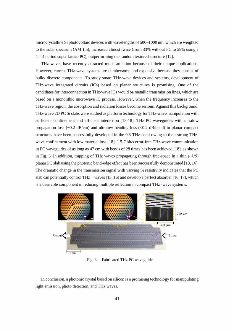
41
microcrystalline Si photovoltaic devices with wavelengths of 500–1000 nm, which are weighted
to the solar spectrum (AM 1.5), increased almost twice (from 33% without PC to 58% using a
4 × 4 period super-lattice PC), outperforming the random textured structure [12].
THz waves have recently attracted much attention because of their unique applications.
However, current THz-wave systems are cumbersome and expensive because they consist of
bulky discrete components. To study smart THz-wave devices and systems, development of
THz-wave integrated circuits (ICs) based on planar structures is promising. One of the
candidates for interconnection in THz-wave ICs would be metallic transmission lines, which are
based on a monolithic microwave IC process. However, when the frequency increases to the
THz-wave region, the absorption and radiation losses become serious. Against this background,
THz-wave 2D PC Si slabs were studied as platform technology for THz-wave manipulation with
sufficient confinement and efficient interaction [13-18]. THz PC waveguides with ultralow
propagation loss (~0.2 dB/cm) and ultralow bending loss (<0.2 dB/bend) in planar compact
structures have been successfully developed in the 0.3-THz band owing to their strong THz-
wave confinement with low material loss [18]. 1.5-Gbit/s error-free THz-wave communication
in PC waveguides of as long as 47 cm with bends of 28 times has been achieved [18], as shown
in Fig. 3. In addition, trapping of THz waves propagating through free-space in a thin (~λ/5)
planar PC slab using the photonic band-edge effect has been successfully demonstrated [13, 16].
The dramatic change in the transmission signal with varying Si resistivity indicates that the PC
slab can potentially control THz waves [13, 16] and develop a perfect absorber [16, 17], which
is a desirable component in reducing multiple reflection in compact THz -wave systems.
In conclusion, a photonic crystal based on silicon is a promising technology for manipulating
light emission, photo detection, and THz waves.
Fig. 3. Fabricated THz PC waveguide.

42
References
[1] M. Fujita, “Nanocavity brightens silicon,” Nature Photon., vol. 7, no. 4, pp. 264–265, 2013.
[2] M. Fujita, Y. Tanaka and S. Noda, “Enhancement of light emission and absorption in silicon
photonic crystals,” 2012 Material Research Society Fall Meeting & Exhibit, no. DD11.01, 2012.
[3] T. Nagatsuma, “Terahertz technologies: present and future,” IEICE Electron. Exp., vol. 8,
no. 14, pp. 1127–1142, 2011.
[4] M. Fujita, B. Gelloz, N. Koshida and S. Noda, “Reduction of surface recombination and
enhancement of light emission in silicon photonic crystals treated by high-pressure water-vapor
annealing,” Appl. Phys. Lett., vol. 97, no. 12, pp. 121111-1–121111-3, 2010.
[5] S. Nakayama, S. Ishida, S. Iwamoto and Y. Arakawa, “Effect of cavity mode volume on
photoluminescence from silicon photonic crystal nanocavities,” Appl. Phys. Lett., vol. 98, no.
17, pp. 171102-1–171102-3, 2011.
[6] R. Lo Savio, S. L. Portalupi, D. Gerace, A. Shakoor, T. F. Krauss, L. O’Faolain, L. C.
Andreani and M. Galli, “Room-temperature emission at telecom wavelengths from silicon
photonic crystal nanocavities,” Appl. Phys. Lett., vol. 98, no. 20, pp. 201106-1–201106-3, 2011.
[7] S. Iwamoto and Y. Arakawa, “Enhancement of light emission from silicon by utilizing
photonic nanostructures,” IEICE Trans. Electron., vol. E95-C, no. 2, pp. 206–212, 2012.
[8] Y. Kurosaka, S. Iwahashi, Y. Liang, K. Sakai, E. Miyai, W. Kunishi, D. Ohnishi, and S.
Noda, “On-chip beam-steering photonic-crystal lasers,” Nature Photon., vol. 4, no. 7, pp. 447–
450 (2010).
[9] H. Kitagawa, M. Fujita, T. Suto, T. Asano and S. Noda, “GaInN photonic-crystal green light-
emitting diodes with small surface recombination effect,” Appl. Phys. Lett., vol. 98, no. 18, pp.
181104-1–181104-3, 2011.
[10] M. De Zoysa, T. Asano, K. Mochizuki, A. Oskooi, T. Inoue, and S. Noda, “Conversion of
broadband to narrowband thermal emission through energy recycling,” Nature Photon., vol. 6,
no. 8, pp. 535-539 (2012).
[11] H. Shigeta, M. Fujita, Y. Tanaka, A. Oskooi, H. Ogawa, Y. Tsuda, and S. Noda,
“Enhancement of photocurrent in ultrathin active-layer photodetecting devices with photonic
crystals,” Appl. Phys. Lett., vol. 101, no. 16, pp. 161103-1–161103-4, 2012.
[12] Y. Tanaka, Y. Kawamoto, M. Fujita, and S. Noda, “Enhancement of broadband optical
absorption in photovoltaic devices by band-edge effect of photonic crystals,” Opt. Express, vol.
21, no. 17, pp. 20111–20118, 2013.
[13] R. Kakimi, M. Fujita, M. Nagai, M. Ashida and T. Nagatsuma, “Trapping a terahertz wave
in a photonic-crystal slab,” IEEE Photonics Conference 2012, no. WQ5, pp. 562–563, 2012.
[14] T. Ishigaki, M. Fujita, M. Nagai, M. Ashida and T. Nagatsuma, “Photonic-crystal slab for

43
terahertz-wave integrated circuits,” IEEE Photonics Conference 2012, no. ThJ3, pp. 774–775,
2012.
[15] A. Suminokura, T. Ishigaki, M. Fujita, and T. Nagatsuma, “Grating coupler for terahertz-
wave integrated circuits,” 2013 Asia-Pacific Radio Science Conference, no. DJ2b-3, 2013.
[16] R. Kakimi, M. Fujita, M. Nagai, M. Ashida and T. Nagatsuma, “Capturing and absorbing
a terahertz wave by a photonic-crystal slab,” 6th Global Symposium on Millimeter Wave 2013,
no. M4-3, 2013.
[17] R. Kakimi, M. Fujita, M. Nagai, M. Ashida and T. Nagatsuma, “Terahertz-wave absorbers
using a photonic crystal slab,” The 10th Conf. Laser and Electro-Optics Pacific Rim, no. WC4-
3, 2013.
[18] K. Tsuruda, T. Ishigaki, A. Suminokura, R. Kakimi, M. Fujita, and T. Nagatsuma,
“Ultralow-loss photonic-crystal waveguides for gigabit terahertz-wave communications,” IEEE
International Topical Meeting on Microwave Photonics 2013, no. Tu2-1, 2013.
D7. Microwave Multiplexers for Readout of Superconducting Detector Array
S. Kohjiro
National Institute of Advanced Industrial Science and Technology
1. TRANSITION EDGE SENSOR (TES) ARRAY
Transition edge sensors (TES), thermal detectors based on the steep temperature dependence
of the resistance of a superconductor at the operation temperature T close to its critical temperature
TC, are attractive for the following applications; 1. X- and -ray calorimeters (photon-counting
mode) with more than one-order-of- magnitude better energy resolution than semiconductor
detectors [1]; 2. Near-infrared photon counters with both the quantum efficiency close to 100%
and the response time less than 200 ns. [2]; 3. Millimeter- and submillimeter-wave bolometers
with more than four-order-of-magnitude better product of (NEP)2× than semiconductor
bolometers cooled below 0.3 K [3], where NEP [W/√Hz] is the noise equivalent power and is
the response time. In both calorimeter and bolometer regimes, arrays with hundred pixels were
developed and a larger-format array is a key issue for future practical use of TES. As the readout
technique for such large number of pixels, a cryogenic multiplexer should be developed since it
decreases the heat flow from 300-K to the cryogenic stage of typically ≈0.1 K through signal

44
wires, resulting in the reduction of volume and power consumption of a cryocooler which
dominates those of TES systems.
2. CRYOGENIC MULTIPLEXERS FOR READOUT OF TES ARRAY
For more than ten years, time-division multiplexing (TDM) [4] and frequency-division
multiplexing (FDM) [5] schemes were studied which operate at typical output channel bandwidth
B≤5 MHz. Multiplexing of semiconductor detectors was based on TDM, since CMOS circuits are
suitable for the fast switch of operating pixels, but difficult to contain high-Q and compact
resonators required for FDM. However, in principle, FDM can exhibit better signal-to-noise ratio
than TDM when the number of multiplexed pixels N increases. This is because all pixels are
simultaneously active in the whole measurement time for FDM [6], while the operating time per
pixel is inversely proportional to N for TDM. Since the surface resistance of superconducting
resonators in microwave region is less than 1/100 of that of a bulk cupper, FDM based on high-
Q superconducting resonators integrated on a chip are attractive [7]. Since the possible number
of multiplexed pixels of FDM is roughly given by N=B/S~kfC/S, increase of fC from ~5 MHz to
~5 GHz is an effective way to increase N, where S is the spacing between neighboring resonances,
fC the middle of resonant frequencies, and k is the ratio of bandwidth to the resonant frequency.
As a termination of a resonator, a normal-type superconducting quantum interference device
(SQUID) with power consumption of ~1 nW/pixel at the same temperature stage as the TES,
typically used for the low-noise TES readout, can be replaced by a dissipation-less-type SQUID,
which has bigger advantage for larger N.
Fig. 1. Microwave multiplexer for TES readout.
3. PIONEERED WORK IN USA

45
The basic concept and operation of this microwave SQUID multiplexer was reported from
National Institute of Standards and Technology (NIST), USA [8]. Mates et al. evaluated noise
current of the SQUID as ~40 pA/√Hz around 100 kHz [9], and demonstrated the flux ramp
modulation which increases the dynamic range of SQUID without the conventional feedback
operation [8, 9]. They also demonstrated the detection of 100-keV radiations from a Gd photon
source with the energy resolution of 60-90 eV by multiplexed two-pixel TES [10].
Though this multiplexer is expected to overcome the limitation of conventional TDM and FDM
schemes, following research and development are necessary for a successful demonstration of the
readout of a large format array. First, the spacing of neighboring resonant frequencies should be
accurately predicted by the design. Next, the noise is desired to decrease less than 10 pA/√Hz
which is the typical value of conventional SQUID-based multiplexers. Finally, a room-
temperature electronics should be developed based on generators of microwave-comb which fit a
series of fC, fast analog-to-digital converters with enough resolution, and up- and a down
converters between the microwave and the baseband [11].
4. JAPANESE WORK
National Institute of Advanced Industrial Science and Technology (AIST), Japan, has started a
study of the microwave multiplexer at 2011. They got the following results:
(1) Finding the design rule which can fit theoretical resonant frequencies to the experimental
ones within +/-0.02% for 4-8 GHz, i.e., the whole readout band [12]. Related result of
NIST’s report was within +/-0.04% in 4.6-5.7 GHz band [13].
(2) Characterization of major noise sources in the system and their improvements [14]. AIST
succeeded in obtaining 31 pA/√Hz for 0.5-1000 kHz at 4 K that is dominated by a Johnson
noise of a resistor in a low-pass filter for preventing the microwave leakage to the TES.
This noise is expected to decrease by a factor of 1/√40 at T=0.1 K.
They are continuing the research for the cooperation of the multiplexer with a TES and
development of room temperature electronics.

46
Fig. 2. Photo (a) and transmission vs. frequency of a multiplexer chip consisting of 16 resonators and
SQUIDs. (c) Modification of transmission with 3 values of SQUID input.
References
[1] D. A. Bennett et al., “A high resolution gamma-ray spectrometer based on superconducting
microcalorimeters,” Rev. Sci. Instrum., 83, 093113, 2012.
[2] D. Fukuda et al., "Titanium-based transition-edge photon number resolving detector with 98 %
detection efficiency with index-matched small-gap fiber coupling," Opt. Exp., 19, 870-875, 2011.
[3] D. Schwan et al., “Millimeter-wave bolometer array receiver for the Atacama pathfinder
experiment Sunyaev-Zel’dovich (APEX-SZ) instrument,” Rev. Sci. Instrum., 82, 091301, 2011.
[4] W. B. Doriese, J. N. Ullom, J. A. Beall, W. D. Duncan, L. Ferreira, G. C. Hilton, et al., “14-
pixel, multiplexed array of gamma-ray microcalorimeters with 47 eV energy resolution at 103
keV,” Appl. Phys. Lett., 90, 193508, 2007.
[5] J. Yoon et al., “Single superconducting quantum interference device multiplexer for arrays of
low-temperature sensors,” Appl. Phys. Lett., 78, 371-373, 2001.
[6] M. F. Cunningham et al., “High-resolution operation of frequency-multiplexed transition-edge
photon sensors,” Appl. Phys. Lett., 81, 159-161, 2002.
[7] J. Zmuidzinas, “Superconducting Microresonators: Physics and Applications,” Annu. Rev.
Cond. Matt. Phys., 3, 169-214, 2012.

47
[8] J. A. B. Mates et al., “Demonstration of a multiplexer of dissipationless superconducting
quantum interference devices,” Appl. Phys. Lett., 92, 023514 1-3, 2008.
[9] J. A. B. Mates, K. D. Irwin, L. R. Vale, G. C. Hilton, J. Gao, and K. W. Lehnert, “Flux-ramp
modulation for SQUID multiplexer,” J. Low Temp. Phys., 167, 707-712, 2012.
[10] O. Noroozian et al., “High-resolution gamma-ray spectroscopy with a microwave-
multiplexed transition-edge sensor array,” Appl. Phys. Lett., 103, 202602, 2013.
[11] S. McHugh et al., “A readout for large arrays of microwave kinetic inductance detectors,”
Rev. Sci. Instrum., 83, 044702, 2012.
[12] F. Hirayama, S. Kohjiro, D. Fukuda, H. Yamamori, S. Nagasawa, and M. Hidaka,
“Microwave SQUID Multiplexer for TES Readout,” IEEE Trans. Appl. Supercond., 23, 2500405,
2013.
[13] K. W. Lehnert, K. D. Irwin, M. A. Castellanos-Beltran, J. A. B. Mates, and L. R. Vale,
“Evaluation of a microwave SQUID multiplexer prototype,” IEEE Trans. Appl. Supercond., 17,
705-709, 2007.
[14] S. Kohjiro et al., in preparation.
D8. High Capacity Optical Fiber Transmission Systems
H. Toda
Doshisha University
In this section, I summarize recent development of high capacity optical fiber transmission
systems and related technologies.
As described in the previous report 3 years ago, digital coherent technique is indispensable for
high capacity transmission systems. All of the transmission experiments described here without
notice are related to digital coherent. In a digital coherent system, influences of dispersion
including polarization mode dispersion, laser phase noise, and Kerr nonlinearity can be
compensated with digital signal processing circuit. Many efforts have been made for
nonlinearity compensation with reduced circuit complexity [1-10]. A field trial of 100-Gbit/s
Ethernet over an optical transport network was conducted using a real-time digital coherent signal
processor [11]. Challenges for the next generation optical transport technologies and
requirements of 100G DWDM systems are reviewed in [12-14].
Forward error collection (FEC) is also very important technology to improve system
performance. Recent progress of soft-decision FEC was reviewed in [15, 16]. Combination of

48
nonlinearity equalizer and FEC was discussed in [17].
High optical spectral efficiency can be achieved with multi-level modulation format. The
spectral efficiencies of 4.7 bit/s/Hz using 16 QAM [18], 9.1 bit/s/Hz using 64 QAM [19], 10
bit/s/Hz using 64 QAM [20, 21], and 14 bit/s/Hz using 256 QAM [22, 23] were demonstrated.
Coherent receiver with digital-delay detection scheme was demonstrated for higher-order
multilevel signal transmission [24-27]. Self-homodyne coherent detection was demonstrated to
reduce receiver complexity [28].
Several techniques were proposed to generate higher-order optical QAM signal [29-32].
LiNbO3 modulators for advanced modulation format were reviewed in [33]. A linear optical IQ
modulator for high-order multilevel modulation [34], IQ-coupling-loss-free polarization-
switched QPSK modulator [35], and dual-carrier dual-polarization IQ modulator [36] were
demonstrated.
As different approaches to improve optical spectral efficiency, nyquist WDM [37, 38] and CO
(coherent optical) -OFDM [39, 40] transmission were demonstrated.
Significant progress has been made in space-division multiplexing over multi-core fiber
(MCF). 109 Tbit/s over 16.8 km [41, 42], 305 Tbit/s over 10.1 km [43], and 1.01 Pbit/s over 52
km [44] transmissions were demonstrated. In [44], the spectral efficiency of 91.4 bit/s/Hz was
obtained with 12-core MCF, 222-channel WDM of 456 Gbit/s PDM-32 QAM single-carrier FDM
signals. For long distance EDFA repeatered transmission, 35.8 Tbit/s over 6,160 km [45, 46]
110.9 Tbit/s over 6,370 km [47], 688 Tbit/s over 1,500 km [48], and 140.7 Tbit/s over 7,326 km
[38] transmissions were demonstrated. Note that the capacity-distance product for [38] and [48]
exceeded 1 Exabit/s•km. These MCF transmission technologies are summarized in [49] and
[50].
Recent research trends for MCF include enlarging effective area, reducing crosstalk, and
reducing propagation loss [51-59]. The achievements are summarized in [60-64]. One
approach to reduce influence of the crosstalk is bidirectional assignment between neighboring
cores [65].
As related technologies to MCF, 7-core EDFA [66-69], 12-core EDFA [70] and optical
connectors for MCF [71] were developed.
On the contrary, transmission experiment with mode-division multiplexing over few-mode
fiber (FMF) [72] and multi-mode fiber [73] were demonstrated. In [74], repeatered transmission
over FMF using a few-mode EDFA was demonstrated. PLC-type multi/demultiplexer for
mode-division multiplexing was reported in [75, 76]. Efforts have been made to reduce
differential mode delay of two-mode fiber [77-79] and four-mode fiber [80] transmission lines
for WDM MIMO system.
In order to further increase the transmission capacity, few-mode multi-core fiber was

49
developed [81-83]. Transmission experiment was made using the fabricated fiber [84, 85].
Recent progress of MCF and FMF technologies are reviewed in [86].
In order to support long distance transmission, efforts are being made to realize pure-silica-
core fiber with low propagation loss and large effective area [87]. Record low loss of 0.149
dB/km at 1550 nm was reported [88].
0.2-V on-off voltage at 25.8 Gbit/s was achieved with newly proposed interferometer-type
electro-absorption modulator [89]. Silica-LiNbO3 hybrid integration [90-94], heterogeneous
integration of active semiconductors with silica-based PLC [95-99], and monolithic integration
using silicon photonics technology [100-102] are promising for future optical fiber transmission
systems.
Phase-sensitive amplifier (PSA) is attractive to enhance signal-to-noise ratio of the received
optical signals. HNLF-based PSA [103, 104] and PPLN-based PSA [105-107] are studied.
Multi-span transmission using PPLN-based PSA was demonstrated in [108, 109].
List of Abbreviations
EDFA Erbium-doped fiber amplifier
FDM Frequency Division Multiplexing
HNLF Highly nonlinear fiber
MIMO Multiple-input multiple-output
OFDM Orthogonal Frequency Division Multiplexing
PDM Polarization Division Multiplexing
PLC Planar lightwave circuit
PPLN Periodically poled Lithium Niobate
QAM Quadrature Amplitude Modulation
QPSK Quadrature Phase-Shift Keying
WDM Wavelength Division Multiplexing
References
[1] Lei Li, Zhenning Tao, Liang Dou, Weizhen Yan, Shoichiro Oda, Takahito Tanimura, Takeshi
Hoshida, and Jens C. Rasmussen, “Implementation Efficient Nonlinear Equalizer Based on
Correlated Digital Backpropagation,” Tech. Digest of OFC/NFOEC 2011, OWW3, Los Angeles,
Mar. 6-10, 2011.
[2] Etsushi Yamazaki, Akihide Sano, Takayuki Kobayashi, Eiji Yoshida, and Yutaka Miyamoto,
“Mitigation of Nonlinearities in Optical Transmission Systems,” Tech. Digest of OFC/NFOEC
2011, OThF1, Los Angeles, Mar. 6-10, 2011.
[3] Takayuki Kobayashi, Akihide Sano, Akihiko Matsuura, Etsushi Yamazaki, Eiji Yoshida,
50
Yutaka Miyamoto, Tadao Nakagawa, Youhei Sakamaki, and Takayuki Mizuno, “120-Gb/s PDM
64-QAM transmission over 1,280 km using multi-staged nonlinear compensation in digital
coherent receiver,” Tech. Digest of OFC/NFOEC 2011, OThF6, Los Angeles, Mar. 6-10, 2011.
[4] Tsuyoshi Yoshida, Takashi Sugihara, Hiroki Goto, Toshiyuki Tokura, Kazuyuki Ishida, and
Takashi Mizuochi, “A Study on Statistical Equalization of Intra-channel Fiber Nonlinearity for
Digital Coherent Optical Systems,” Tech. Digest of ECOC 2011, Tu.3.A.1, Geneva, Sept. 18-22,
2011.
[5] Weizhen Yan, Zhenning Tao, Liang Dou, Lei Li, Shoichiro Oda, Takahito Tanimura, Takeshi
Hoshida, and Jens C. Rasmussen, “Low Complexity Digital Perturbation Back-propagation,”
Tech. Digest of ECOC 2011, Tu.3.A.2, Geneva, Sept. 18-22, 2011.
[6] Liang Dou, Zhenning Tao, Weizhen Yan, Lei Li, Takeshi Hoshida, and Jens C. Rasmussen,
“Pre-Distortion Method for Intra-channel Nonlinearity Compensation with Phase-rotated
Perturbation Term,” Tech. Digest of OFC/NFOEC 2012, OTh3C.2, Los Angeles, Mar. 4-8, 2012.
[7] Eduardo Mateo, Ming-Fang Huang, Fatih Yaman, Ting Wang, Yoshiaki Aono, and Tsutomu
Tajima, “Nonlinearity compensation using very-low complexity backward propagation in
dispersion managed links,” Tech. Digest of OFC/NFOEC 2012, OTh3C.4, Los Angeles, Mar. 4-
8, 2012.
[8] Hisao Nakashima, Tomofumi Oyama, Yuichi Akiyama, Shoichiro Oda, Liang Dou, Yangyang
Fan, Zhenning Tao, Takeshi Hoshida, and Jens C. Rasmussen, “PMD and PDL Tolerances of
Transmitter-side Non-linear Mitigation in 112 Gb/s DP-QPSK Transmission,” Tech. Digest of
ECOC 2012, We.3.C.5, Amsterdam, Sept. 16-20, 2012.
[9] Liang Dou, Zhenning Tao, Yuichi Akiyama, Shoichiro Oda, Yangyang Fan, Tomofumi
Oyama, Hisao Nakashima, Takeshi Hoshida, and Jens C. Rasmussen, “Real-Time 112Gb/s
DWDM Coherent Transmission with 40% Extended Reach by Transmitter-side Low-Complexity
Nonlinear Mitigation ,” Tech. Digest of ECOC 2012, Th.1.D.3, Amsterdam, Sept. 16-20, 2012.
[10] Takeshi Hoshida, Liang Dou, Weizhen Yan, Lei Li, Zhenning Tao, Shoichiro Oda, Hisao
Nakashima, Chihiro Ohshima, Tomofumi Oyama, and Jens C. Rasmussen, “Advanced and
feasible signal processing algorithm for nonlinear mitigation,” Tech. Digest of OFC/NFOEC
2013, OTh3C.3, Anaheim, Mar. 17-21, 2013.
[11] Etsushi Yamazaki, Shogo Yamanaka, Yoshiaki Kisaka, Tadao Nakagawa, Koichi Murata,
Eiji Yoshida, Toshikazu Sakano, Masahito Tomizawa, Yutaka Miyamoto, Shinji Matsuoka,
Junichiro Matsui, Atsufumi Shibayama, Jun-ichi Abe, Yuichi Nakamura, Hidemi Noguchi,
Kiyoshi Fukuchi, Hiroshi Onaka, Katsumi Fukumitsu, Kousuke Komaki, Osamu Takeuchi,
Yuichiro Sakamoto, Hisao Nakashima, Takashi Mizuochi, Kazuo Kubo, Yoshikuni Miyata,
Hiroshi Nishimoto, Susumu Hirano, and Kiyoshi Onohara, “Fast optical channel recovery in field
demonstration of 100-Gbit/s Ethernet over OTN using real-time DSP,” Optics Express, Vol. 19,

51
Issue 14, pp. 13179-13184, 2011.
[12] Yutaka Miyamoto, Akihide Sano, and Takayuki Kobayashi, “The Challenge for the Next
Generation OTN Based on 400Gbps and Beyond,” Tech. Digest of OFC/NFOEC 2012, NTu2E.3,
Los Angeles, Mar. 4-8, 2012.
[13] Masahito Tomizawa, “DSP Aspects for Deployment of 100G-DWDM Systems in Carrier
Networks,” Tech. Digest of OFC/NFOEC 2012, NTh1I.1, Los Angeles, Mar. 4-8, 2012.
[14] Akihide Sano, Takayuki Kobayashi, and Yutaka Miyamoto, “400-Gb/s/ch High Capacity
Transport Technologies,” Tech. Digest of ECOC 2012, Mo.2.C.1, Amsterdam, Sept. 16-20, 2012.
[15] Takashi Mizuochi, Yoshikuni Miyata, Kazuo Kubo, Takashi Sugihara, Kiyoshi Onohara,
and Hideo Yoshida, “Progress in Soft-Decision FEC,” Tech. Digest of OFC/NFOEC 2011,
NWC2, Los Angeles, Mar. 6-10, 2011.
[16] Takashi Mizuochi, Takashi Sugihara, Yoshikuni Miyata, Kazuo Kubo, Kiyoshi Onohara,
Susumu Hirano, Hideo Yoshida, Tsuyoshi Yoshida, and Toshiyuki Ichikawa, “Evolution and
status of forward error correction,” Tech. Digest of OFC/NFOEC 2012, OTu2A.6, Los Angeles,
Mar. 4-8, 2012.
[17] Takashi Sugihara, Tsuyoshi Yoshida, and Takashi Mizuochi, “Collaborative Signal
Processing with FEC in Digital Coherent Systems,” Tech. Digest of OFC/NFOEC 2013, OM2B.3,
Anaheim, Mar. 17-21, 2013.
[18] Shaoliang Zhang, Ming-Fang Huang, Fatih Yaman, Eduardo Mateo, Dayou Qian, Yequn
Zhang, Lei Xu, Yin Shao, Ivan Djordjevic, Ting Wang, Yoshihisa Inada, Takanori Inoue, Takaaki
Ogata, and Yasuhiro Aoki, “40×117.6 Gb/s PDM-16QAM OFDM Transmission over 10,181 km
with Soft-Decision LDPC Coding and Nonlinearity Compensation,” Tech. Digest of
OFC/NFOEC 2012, PDP5C.4, Los Angeles, Mar. 4-8, 2012.
[19] Akihide Sano, Takayuki Kobayashi, Shogo Yamanaka, Akihiko Matsuura, Hiroto Kawakami,
Yutaka Miyamoto, Koichi Ishihara, and Hiroji Masuda, “102.3-Tb/s (224 x 548-Gb/s) C- and
Extended L-band All-Raman Transmission over 240 km Using PDM-64QAM Single Carrier
FDM with Digital Pilot Tone,” Tech. Digest of OFC/NFOEC 2012, PDP5C.3, Los Angeles, Mar.
4-8, 2012.
[20] Takayuki Kobayashi, Akihide Sano, Akihiko Matsuura, Mitsuteru Yoshida, Toshikazu
Sakano, Hirokazu Kubota, Yutaka Miyamoto, Koichi Ishihara, Masato Mizoguchi, and Munehiko
Nagatani, “45.2Tb/s C-band WDM transmission over 240km using 538Gb/s PDM-64QAM single
carrier FDM signal with digital pilot tone,” Tech. Digest of ECOC 2011, Th.13.C.6, Geneva, Sept.
18-22, 2011.
[21] Takayuki Kobayashi, Akihide Sano, Akihiko Matsuura, Yutaka Miyamoto, and Koichi
Ishihara, “High-Order QAM Transmission for Spectrally-efficient and High-capacity Transport,”
Tech. Digest of OFC/NFOEC 2012, OM2A.3, Los Angeles, Mar. 4-8, 2012.

52
[22] Tatsunori Omiya, Masato Yoshida, and Masataka Nakazawa, “400 Gbit/s 256 QAM-OFDM
Transmission over 720 km with a 14 bit/s/Hz Spectral Efficiency Using an Improved FDE
Technique,” Tech. Digest of OFC/NFOEC 2013, OTh4E.1, Anaheim, Mar. 17-21, 2013.
[23] Tatsunori Omiya, Masato Yoshida, and Masataka Nakazawa, “400 Gbit/s 256 QAM-OFDM
transmission over 720 km with a 14 bit/s/Hz spectral efficiency by using high-resolution FDE,”
Optics Express, Vol. 21, Issue 3, pp. 2632-2641, 2013.
[24] Nobuhiko Kikuchi, Shinya Sasaki, and Tetsuya Uda, “Phase-Noise Tolerant Coherent
Polarization-Multiplexed 16QAM Transmission with Digital Delay-Detection,” Tech. Digest of
ECOC 2011, Tu.3.A.5, Geneva, Sept. 18-22, 2011.
[25] Nobuhiko Kikuchi, Shinya Sasaki, and Tetsuya Uda, “Polarization-Multiplexed 32QAM and
16PSK Signaling with Coherent Receiver using Digital-Delay Detection,” Tech. Digest of
OFC/NFOEC 2012, OM2A.1, Los Angeles, Mar. 4-8, 2012.
[26] Nobuhiko Kikuchi, Shinya Sasaki, and Tetsuya Uda, “Improvement of Tolerance to Intra-
channel Non-linear Effect of Coherent Higher-order Multilevel Signaling with Digital Delay-
Detection,” Tech. Digest of ECOC 2012, We.3.C.1, Amsterdam, Sept. 16-20, 2012.
[27] Nobuhiko Kikuchi, “Higher-order Multilevel Signal Transmission using Coherent Receiver
with Digital-Delay Detection,” Tech. Digest of OFC/NFOEC 2013, OTh4E.5, Anaheim, Mar. 17-
21, 2013.
[28] Benjamin J. Puttnam, Jose-Manuel Delgado-Mendinueta, Jun Sakaguchi, Ruben S. Luís,
Werner Klaus, Yoshinari Awaji, Naoya Wada, Atsushi Kanno, and Tetsuya Kawanishi, “105Tb/s
Transmission System Using Low-cost, MHz Linewidth DFB Lasers Enabled by Self-Homodyne
Coherent Detection and a 19-Core Fiber,” Tech. Digest of OFC/NFOEC 2013, OW1I.1, Anaheim,
Mar. 17-21, 2013.
[29] Eiichi Yamada, Yasuo Shibata, Kei Watanabe, Takako Yasui, Akira Ohki, Hiroyasu
Mawatari, Shigeru Kanazawa, Ryuzo Iga, and Hiroyuki Ishii, “Demonstration of 50 Gbit/s
16QAM Signal Generation by Novel 16QAM Generation Method using a Dual-Drive InP Mach-
Zehnder Modulator,” Tech. Digest of OFC/NFOEC 2011, OMU1, Los Angeles, Mar. 6-10, 2011.
[30] Guo-Wei Lu, Takahide Sakamoto, and Tetsuya Kawanishi, “Optical 64QAM Transmitter
using Tandem IQ Modulators with Balanced Complexity in Electronics and Optics,” Tech. Digest
of OFC/NFOEC 2013, OM3C.2, Anaheim, Mar. 17-21, 2013.
[31] Guo-Wei Lu, Takahide Sakamoto, and Tetsuya Kawanishi, “Flexible high-order QAM
transmitter using tandem IQ modulators for generating 16/32/36/64-QAM with balanced
complexity in electronics and optics,” Optics Express, Vol. 21, Issue 5, pp. 6213-6223, 2013.
[32] Hyeon Y. Choi, Takehiro Tsuritani, and Itsuro Morita, “A New Multi-Purpose Optical
Transmitter for Higher-Order QAM Generation,” Tech. Digest of OFC/NFOEC 2013, OM3C.4,
Anaheim, Mar. 17-21, 2013.

53
[33] Hiroshi Yamazaki, Takashi Goh, and Takashi Saida, “Optical Modulators for Advanced
Digital Coherent Transmission Systems,” Tech. Digest of ECOC 2013, We.1.B.1, London, Sept.
22-26, 2013.
[34] Hiroshi Yamazaki, Hiroshi Takahashi, Takashi Goh, Yasuaki Hashizume, Shinji Mino, and
Yutaka Miyamoto, “Linear Optical IQ Modulator for High-Order Multilevel Coherent
Transmission,” Tech. Digest of OFC/NFOEC 2013, OM3C.1, Anaheim, Mar. 17-21, 2013.
[35] Hiroshi Yamazaki, Takashi Goh, Takashi Saida, Yasuaki Hashizume, and Shinji Mino, “IQ-
Coupling-Loss-Free Polarization-Switched QPSK Modulator,” Tech. Digest of OFC/NFOEC
2012, PDP5A.8, Los Angeles, Mar. 4-8, 2012.
[36] Hiroshi Yamazaki, Takashi Goh, Takashi Saida, Yasuaki Hashizume, Shinji Mino,
Munehiko Nagatani, Hideyuki Nosaka, and Koichi Murata, “Dual-carrier Dual-polarization IQ
Modulator Driven with High-speed DACs for 400-Gb/s Applications,” Tech. Digest of ECOC
2012, We.3.E.1, Amsterdam, Sept. 16-20, 2012.
[37] Koji Igarashi, Yojiro Mori, Kazuhiro Katoh, and Kazuro Kikuchi, “Bit-error Rate
Performance of Nyquist Wavelength-Division Multiplexed Quadrature Phase-Shift Keying
Optical Signals,” Tech. Digest of OFC/NFOEC 2011, OMR6, Los Angeles, Mar. 6-10, 2011.
[38] K. Igarashi, T. Tsuritani, I. Morita, Y. Tsuchida, K. Maeda, M. Tadakuma, T. Saito, K.
Watanabe, K. Imamura, R. Sugizaki, and M Suzuki, “1.03-Exabit/s_km Super-Nyquist-WDM
Transmission over 7,326-km Seven-Core Fiber,” Tech. Digest of ECOC 2013, PD3.E.3, London,
Sept. 22-26, 2013.
[39] Wei-Ren Peng, Hidenori Takahashi, Itsuro Morita, and Hideaki Tanaka, “117-Gb/s Optical
OFDM Super-channel Transmission over 1200-km SSMF Using Direct Detection and EDFA-
Only Amplification,” Tech. Digest of OFC/NFOEC 2011, OThX1, Los Angeles, Mar. 6-10, 2011.
[40] Hidenori Takahashi, Wei-Ren Peng, Itsuro Morita, and Hideaki Tanaka, “7 x 463-Gbit/s
Optical OFDM transmission at 100-GHz WDM spacing over 960 km of SSMF with EDFA-only
Amplification,” Tech. Digest of ECOC 2011, Th.11.B.6, Geneva, Sept. 18-22, 2011.
[41] Jun Sakaguchi, Yoshinari Awaji, Naoya Wada, Atsushi Kanno, Tetsuya Kawanishi, Tetsuya
Hayashi, Toshiki Taru, Tetsuya Kobayashi, and Masayuki Watanabe, “109-Tb/s (7x97x172-Gb/s
SDM/WDM/PDM) QPSK transmission through 16.8-km homogeneous multi-core fiber,” Tech.
Digest of OFC/NFOEC 2011, PDPB6, Los Angeles, Mar. 6-10, 2011.
[42] Jun Sakaguchi, Yoshinari Awaji, Naoya Wada, Atsushi Kanno, Tetsuya Kawanishi, Tetsuya
Hayashi, Toshiki Taru, Tetsuya Kobayashi, and Masayuki Watanabe, “Space Division
Multiplexed Transmission of 109-Tb/s Data Signals Using Homogeneous Seven-Core Fiber,”
Journal of Lightwave Technology, Vol. 30, Issue 4, pp. 658-665, 2012.
[43] Jun Sakaguchi, Benjamin J. Puttnam, Werner Klaus, Yoshinari Awaji, Naoya Wada, Atsushi
Kanno, Tetsuya Kawanishi, Katsunori Imamura, Harumi Inaba, Kazunori Mukasa, Ryuichi

54
Sugizaki, Tetsuya Kobayashi, and Masayuki Watanabe, “19-core fiber transmission of
19x100x172-Gb/s SDM-WDM-PDM-QPSK signals at 305Tb/s,” Tech. Digest of OFC/NFOEC
2012, PDP5C.1, Los Angeles, Mar. 4-8, 2012.
[44] Hidehiko Takara, Akihide Sano, Takayuki Kobayashi, Hirokazu Kubota, Hiroto Kawakami,
Akihiko Matsuura, Yutaka Miyamoto, Yoshiteru Abe, Hirotaka Ono, Kota Shikama, Yukihiro
Goto, Kyozo Tsujikawa, Yusuke Sasaki, Itaru Ishida, Katsuhiro Takenaga, Shoichiro Matsuo,
Kunimasa Saitoh, Masanori Koshiba, and Toshio Morioka, “1.01-Pb/s (12 SDM/222 WDM/456
Gb/s) Crosstalk-managed Transmission with 91.4-b/s/Hz Aggregate Spectral Efficiency,” Tech.
Digest of ECOC 2012, Th.3.C.1, Amsterdam, Sept. 16-20, 2012.
[45] Hidenori Takahashi, Takehiro Tsuritani, Emmanuel Le Taillandier de Gabory, Toshiharu Ito,
Wei-Ren Peng, Koji Igarashi, Koki Takeshima, Yu Kawaguchi, Itsuro Morita, Yukihiro Tsuchida,
Yu Mimura, Koichi Maeda, Tsunetoshi Saito, Kengo Watanabe, Katsunori Imamura, Ryuichi
Sugizaki, and Masatoshi Suzuki, “First Demonstration of MC-EDFA-Repeatered SDM
Transmission of 40 x 128-Gbit/s PDM-QPSK Signals per Core over 6,160-km 7-core MCF,”
Tech. Digest of ECOC 2012, Th.3.C.3, Amsterdam, Sept. 16-20, 2012.
[46] H. Takahashi, T. Tsuritani, E. L. T. de Gabory, T. Ito, W. R. Peng, K. Igarashi, K. Takeshima,
Y. Kawaguchi, I. Morita, Y. Tsuchida, Y. Mimura, K. Maeda, T. Saito, K. Watanabe, K. Imamura,
R. Sugizaki, and M. Suzuki, “First demonstration of MC-EDFA-repeatered SDM transmission of
40 x 128-Gbit/s PDM-QPSK signals per core over 6,160-km 7-core MCF,” Optics Express, Vol.
21, Issue 1, pp. 789-795, 2013.
[47] K. Igarashi, K. Takeshima, T. Tsuritani, H. Takahashi, S. Sumita, I. Morita, Y. Tsuchida, M.
Tadakuma, K. Maeda, T. Saito, K. Watanabe, K. Imamura, R. Sugizaki, M. Suzuki, “Seven-Core
Fiber with Enlarged Aeff and Full-C-band Seven-Core EDFA for 100-Tbit/s-Class Transoceanic
Transmission,” Tech. Digest of ECOC 2013, Mo.3.A.2, London, Sept. 22-26, 2013.
[48] T. Kobayashi, H. Takara, A. Sano, T. Mizuno, H. Kawakami, Y Miyamoto, K. Hiraga, Y.
Abe, H. Ono, M. Wada, Y. Sasaki, I. Ishida, K. Takenaga, S. Matsuo, K. Saitoh, M. Yamada, H.
Masuda, T. Morioka, “2 x 344 Tb/s Propagation-direction Interleaved Transmission over 1500-
km MCF Enhanced by Multicarrier Full Electric-field Digital Back-propagation,” Tech. Digest
of ECOC 2013, PD3.E.4, London, Sept. 22-26, 2013.
[49] Jun Sakaguchi, Benjamin J. Puttnam, Werner Klaus, Jose-Manuel Delgado-Mendinueta,
Yoshinari Awaji, Naoya Wada, Atsushi Kanno, and Tetsuya Kawanishi, “Large-capacity
transmission over a 19-core fiber,” Tech. Digest of OFC/NFOEC 2013, OW1I.3, Anaheim, Mar.
17-21, 2013.
[50] Hidehiko Takara, “Multi-core Fiber Transmission Technologies for Peta b/s per Fiber
Capacity,” Tech. Digest of ECOC 2013, We.2.D.3, London, Sept. 22-26, 2013.
[51] Tetsuya Hayashi, Toshiki Taru, Osamu Shimakawa, Takashi Sasaki, and Eisuke Sasaoka,

55
“Low-Crosstalk and Low-Loss Multi-Core Fiber Utilizing Fiber Bend,” Tech. Digest of
OFC/NFOEC 2011, OWJ3, Los Angeles, Mar. 6-10, 2011.
[52] Tetsuya Hayashi, Toshiki Taru, Osamu Shimakawa, Takashi Sasaki, and Eisuke Sasaoka,
“Ultra-Low-Crosstalk Multi-Core Fiber Feasible to Ultra-Long-Haul Transmission,” Tech.
Digest of OFC/NFOEC 2011, PDPC2, Los Angeles, Mar. 6-10, 2011.
[53] Katsunori Imamura, Kazunori Mukasa, and Ryuichi Sugizaki, “Trench Assisted Multi-Core
Fiber with Large Aeff over 100 μm2 and Low Attenuation Loss,” Tech. Digest of ECOC 2011,
Mo.1.LeCervin.1, Geneva, Sept. 18-22, 2011.
[54] Katsuhiro Takenaga, Yoko Arakawa, Yusuke Sasaki, Shoji Tanigawa, Shoichiro Matsuo,
Kunimasa Saitoh, and Masanori Koshiba, “A Large Effective Area Multi-Core Fibre with an
Optimised Cladding Thickness,” Tech. Digest of ECOC 2011, Mo.1.LeCervin.2, Geneva, Sept.
18-22, 2011.
[55] Katsunori Imamura, Harumi Inaba, Kazunori Mukasa, and Ryuichi Sugizaki, “Multi Core
Fiber with Large Aeff of 140 μm2 and Low Crosstalk,” Tech. Digest of ECOC 2012, Mo.1.F.2,
Amsterdam, Sept. 16-20, 2012.
[56] Tetsuya Hayashi, Toshiki Taru, Osamu Shimakawa, Takashi Sasaki, and Eisuke Sasaoka,
“Low-Loss and Large-Aeff Multi-core Fiber for SNR Enhancement,” Tech. Digest of ECOC
2012, Mo.1.F.3, Amsterdam, Sept. 16-20, 2012.
[57] T. Hayashi, T. Taru, O. Shimakawa, T. Sasaki, and E. Sasaoka, E., “Design and fabrication
of ultra-low crosstalk and low-loss multi-core fiber,” Optics Express, Vol. 19, Issue 17, pp.
16576-16592, 2013.
[58] K. Takenaga, Y. Arakawa, S. Tanigawa, N. Guan, S. Matsuo, K. Saitoh, M. Koshiba, “An
investigation on crosstalk in multi-core fibers by introducing random fluctuation along
longitudinal direction,” IEICE Transactions on Communications, Vol. E94-B, Issue 2, pp. 409-
416 (2011).
[59] M. Koshiba, K. Saitoh, K. Takenaga, and S. Matsuo, “Multi-core fiber design and analysis:
Coupledmode theory and coupled-power theory,” Optics Express, Vol. 19, Issue 26, pp. B102-
B111, 2011.
[60] Kazunori Mukasa, Katsunori Imamura, Yukihiro Tsuchida, and Ryuichi Sugizaki, “Multi-
Core Fibers for Large Capacity SDM,” Tech. Digest of OFC/NFOEC 2011, OWJ1, Los Angeles,
Mar. 6-10, 2011.
[61] Masanori Koshiba, Kunimasa Saitoh, Katsuhiro Takenaga, and Shoichiro Matsuo, “Multi-
core Fiber Design and Analysis,” Tech. Digest of ECOC 2011, Mo.1.LeCervin.5, Geneva, Sept.
18-22, 2011.
[62] Tetsuya Hayashi, Takashi Sasaki, and Eisuke Sasaoka, “Multi-Core Fibers for High Capacity
Transmission,” Tech. Digest of OFC/NFOEC 2012, OTu1D.4, Los Angeles, Mar. 4-8, 2012.

56
[63] Katsuhiro Takenaga, Shoichiro Matsuo, Kunimasa Saitoh, and Masanori Koshiba,
“Characterisation of MC Fibers: New Techniques and Challenges,” Tech. Digest of OFC/NFOEC
2012, OTu1D.5, Los Angeles, Mar. 4-8, 2012.
[64] H Takahashi, and T Tsuritani, “Ultra-Long-Haul MCF Transmission Systems,” Tech. Digest
of ECOC 2013, Tu.1.D.4, London, Sept. 22-26, 2013.
[65] Toshiharu Ito, Emmanuel Le Taillandier de Gabory, Manabu Arikawa, Yoichi Hashimoto,
and Kiyoshi Fukuchi, “Reduction of Influence of Inter-core Cross-talk in MCF with Bidirectional
Assignment between Neighboring Cores,” Tech. Digest of OFC/NFOEC 2013, OTh3K.2,
Anaheim, Mar. 17-21, 2013.
[66] Yu Mimura, Yukihiro Tsuchida, Koichi Maeda, Ryo Miyabe, Keiichi Aiso, Hiroshi
Matsuura, and Ryuichi Sugizaki, “Batch Multicore Amplification with Cladding-Pumped
Multicore EDF,” Tech. Digest of ECOC 2012, Tu.4.F.1, Amsterdam, Sept. 16-20, 2012.
[67] Yukihiro Tsuchida, Koichi Maeda, Kengo Watanabe, Tsunetoshi Saito, Shigeto Matsumoto,
Keiichi Aiso, Yu Mimura, and Ryuichi Sugizaki, “Simultaneous 7-Core Pumped Amplification
in Multicore EDF through Fibre Based Fan-In/Out,” Tech. Digest of ECOC 2012, Tu.4.F.2,
Amsterdam, Sept. 16-20, 2012.
[68] Yukihiro Tsuchida, Koichi Maeda, Kengo Watanabe, Toshiharu Ito, Kiyoshi Fukuchi,
Masato Yoshida, Yu Mimura, Ryuichi Sugizaki, and Masataka Nakazawa, “Multicore EDFA for
DWDM Transmission in Full C-band,” Tech. Digest of OFC/NFOEC 2013, JW2A.16, Anaheim,
Mar. 17-21, 2013.
[69] S. Takasaka, H. Matsuura, W. Kumagai, M. Tadakuma, Y. Mimura, Y. Tsuchida, K. Maeda,
R. Miyabe, K. Aiso, K. Doi, and R. Sugizaki, “Cladding-pumped seven-core EDFA using a
multimode pump light coupler ,” Tech. Digest of ECOC 2013, We.4.A.5, London, Sept. 22-26,
2013.
[70] H. Ono, K. Takenaga, K. Ichii, S. Matsuo, T. Takahashi, H. Masuda, M. Yamada, “12-Core
Double-Clad Er/Yb-Doped Fiber Amplifier Employing Free-space Coupling Pump/Signal
Combiner Module,” Tech. Digest of ECOC 2013, We.4.A.4, London, Sept. 22-26, 2013.
[71] Kota Shikama, Yoshiteru Abe, Shuichi Yanagi, and Tetsuo Takahashi, “Physical-contact
conditions for multicore fiber optical connectors,” Tech. Digest of OFC/NFOEC 2013, OM3I.1,
Anaheim, Mar. 17-21, 2013.
[72] Nobutomo Hanzawa, Kunimasa Saitoh, Taiji Sakamoto, Takashi Matsui, Shigeru Tomita,
and Masanori Koshiba, “Demonstration of mode-division multiplexing transmission over 10 km
two-mode fiber with mode coupler,” Tech. Digest of OFC/NFOEC 2011, OWA4, Los Angeles,
Mar. 6-10, 2011.
[73] Takayoshi Mori, Taiji Sakamoto, Takashi Yamamoto, and Shigeru Tomita, “Wideband
WDM Coherent Optical MIMO Transmission over GI-MMF by Using Selective Mode

57
Excitation,” Tech. Digest of OFC/NFOEC 2012, OTu2C.3, Los Angeles, Mar. 4-8, 2012.
[74] Ezra Ip, Ming-jun Li, Yue-Kai Huang, Akihiro Tanaka, Eduardo Mateo, William Wood,
Junqiang Hu, Yutaka Yano, and Konstantin Koreshkov, “146λx6x19-Gbaud Wavelength- and
Mode-Division Multiplexed Transmission over 10x50-km Spans of Few-Mode Fiber with a Gain-
Equalized Few-Mode EDFA,” Tech. Digest of OFC/NFOEC 2013, PDP5A.2, Anaheim, Mar. 17-
21, 2013.
[75] Takui Uematsu, Kunimasa Saitoh, Nobutomo Hanzawa, Taiji Sakamoto, Takashi Matsui,
Kyozo Tsujikawa, and Masanori Koshiba, “Low-loss and broadband PLC-type mode
(de)multiplexer for mode-division multiplexing transmission,” Tech. Digest of OFC/NFOEC
2013, OTh1B.5, Anaheim, Mar. 17-21, 2013.
[76] Nobutomo Hanzawa, Kunimasa Saitoh, Taiji Sakamoto, Kyozo Tsujikawa, Takui Uematsu,
Masanori Koshiba, and Fumihiko Yamamoto, “Three-mode PLC-type Multi/demultiplexer for
Mode-division Multiplexing Transmission,” Tech. Digest of ECOC 2013, Tu.1.B.3, London, Sept.
22-26, 2013.
[77] Taiji Sakamoto, Takayoshi Mori, Takashi Yamamoto, and Shigeru Tomita, “Differential
Mode Delay Managed Transmission Line for Wide-band WDM-MIMO System,” Tech. Digest
of OFC/NFOEC 2012, OM2D.1, Los Angeles, Mar. 4-8, 2012.
[78] Ryo Maruyama, Nobuo Kuwaki, Shoichiro Matsuo, Kiminori Sato, and Masaharu Ohashi,
“DMD Free Transmission Line Composed of TMFs with Large Effective Area for MIMO
Processing,” Tech. Digest of ECOC 2012, Tu.1.F.2, Amsterdam, Sept. 16-20, 2012.
[79] R. Maruyama, T. Shoji, N. Kuwaki, S. Matsuo, K. Sato, and M. Ohashi, “Design and
Fabrication of Long DMD Maximally Flattened Two-Mode Optical Fibres suitable for MIMO
Processing,” Tech. Digest of ECOC 2013, Mo.4.A.3, London, Sept. 22-26, 2013.
[80] Takayoshi Mori, Taiji Sakamoto, Masaki Wada, Takashi Yamamoto, and Fumihiko
Yamamoto, “Low DMD Four LP Mode Transmission Fiber for Wide-band WDM-MIMO
System,” Tech. Digest of OFC/NFOEC 2013, OTh3K.1, Anaheim, Mar. 17-21, 2013.
[81] Yusuke Sasaki, Katsuhiro Takenaga, Ning Guan, Shoichiro Matsuo, Kunimasa Saitoh, and
Masanori Koshiba, “Large-Effective-Area Uncoupled Few-Mode Multi-Core Fiber,” Tech.
Digest of ECOC 2012, Tu.1.F.3, Amsterdam, Sept. 16-20, 2012.
[82] Shoichiro Matsuo; Fujikura, “Recent Progress in Multi core and Few mode Fiber,” Tech.
Digest of OFC/NFOEC 2013, OM3I.3, Anaheim, Mar. 17-21, 2013.
[83] Y. Sasaki, Y. Ammma, K. Takenaga, S. Matsuo, K. Saitoh, M. Koshiba, “Trench-assisted
Low-crosstalk Few-mode Multicore Fiber,” Tech. Digest of ECOC 2013, Mo.3.A.5, London,
Sept. 22-26, 2013.
[84] Roland Ryf, Alberto Sierra, Rene-Jean Essiambre, Alan Gnauck, Sebastian Randel, Mina
Esmaeelpour, Sami Mumtaz, Peter J. Winzer, Roger Delbue, Peter Pupalaikis, Anirudh Sureka,

58
Tetsuya Hayashi, Toshiki Taru, and Takashi Sasaki, “Coherent 1200-km 6 x 6 MIMO Mode-
Multiplexed Transmission over 3-Core Microstructured Fiber,” Tech. Digest of ECOC 2011,
Th.13.C.1, Geneva, Sept. 18-22, 2011.
[85] Roland Ryf, Rene Essiambre, Alan Gnauck, Sebastian Randel, Miguel A. Mestre, Christian
Schmidt, Peter Winzer, Roger Delbue, Peter Pupalaikis, Anirudh Sureka, Tetsuya Hayashi,
Toshiki Taru, and Takashi Sasaki, “Space-Division Multiplexed Transmission over 4200 km 3-
Core Microstructured Fiber,” Tech. Digest of OFC/NFOEC 2012, PDP5C.2, Los Angeles, Mar.
4-8, 2012.
[86] T. Morioka, Y. Awaji, R. Ryf, P. Winzer, D. Richardson, and F. Poletti, “Enhancing optical
communications with brand new fibers,” IEEE Communications Magazine, Vol. 50, Issue 2, pp.
S31-S42, 2012.
[87] Yoshinori Yamamoto, Masaaki Hirano, and Takashi Sasaki, “A New Class of Optical Fiber
to Support Large Capacity Transmission,” Tech. Digest of OFC/NFOEC 2011, OWA6, Los
Angeles, Mar. 6-10, 2011.
[88] Masaaki Hirano, Tetsuya Haruna, Yoshiaki Tamura, Takehiko Kawano, Satoshi Ohnuki,
Yoshinori Yamamoto, Yasushi Koyano, and Takashi Sasaki, “Record Low Loss, Record High
FOM Optical Fiber with Manufacturable Process,” Tech. Digest of OFC/NFOEC 2013, PDP5A.7,
Anaheim, Mar. 17-21, 2013.
[89] Y. Ueda, T. Fujisawa, S. Kanazawa, W. Kobayashi, K. Takahata, and H. Ishii, “Very-Low-
Voltage Operation of Mach-Zehnder Interferometer-Type Electroabsorption Modulator,” Tech.
Digest of ECOC 2013, We.1.B.2, London, Sept. 22-26, 2013.
[90] Hiroshi Yamazaki, Takashi Yamada, Takashi Goh, and Shinji Mino, “Multilevel Optical
Modulator with PLC and LiNbO3 Hybrid Integrated Circuit,” Tech. Digest of OFC/NFOEC 2011,
OWV1, Los Angeles, Mar. 6-10, 2011.
[91] Takashi Goh, Hiroshi Yamazaki, Toshimi Kominato, and Shinji Mino, “Novel Flexible-
Format Optical Modulator with Selectable Combinations of Carrier Numbers and Modulation
Levels Based on Silica-PLC and LiNbO3 Hybrid Integration,” Tech. Digest of OFC/NFOEC
2011, OWV2, Los Angeles, Mar. 6-10, 2011.
[92] Takashi Goh, “Flexible-format Optical Modulator using Silica-LiNbO3 Hybrid Integration
Technology,” Tech. Digest of OFC/NFOEC 2012, OM3J.4, Los Angeles, Mar. 4-8, 2012.
[93] Ken Tsuzuki, Takashi Saida, Motohaya Ishii, Takashi Goh, Hiroshi Yamazaki, Yoshoyuki
Doi, Atsushi Aratake, Takao Fukumitsu, Munehisa Tamura, and Shinji Mino, “Design and
Evaluation of Highly Reliable Silica-LiNbO3 Hybrid Modulators for Advanced Formats,” Tech.
Digest of OFC/NFOEC 2012, OM3J.5, Los Angeles, Mar. 4-8, 2012.
[94] Shinji Mino, Hiroshi Yamazaki, Takashi Goh, and Takashi Saida, “Transmitter Synthesis for
Advanced Modulation Formats Utilizing Silica-LiNbO3 Hybrid Integration Technology,” Tech.

59
Digest of OFC/NFOEC 2013, OM3C.3, Anaheim, Mar. 17-21, 2013.
[95] Yu Kurata, Yusuke Nasu, Munehisa Tamura, Haruki Yokoyama, and Yoshifumi Muramoto,
“Heterogeneous integration of high-speed InP PDs on silica-based planar lightwave circuit
platform,” Tech. Digest of ECOC 2011, Th.12.LeSaleve.5, Geneva, Sept. 18-22, 2011.
[96] Eiichi Yamada, Shigeru Kanazawa, Akira Ohki, Kei Watanabe, Yusuke Nasu, Nobuhiro
Kikuchi, Yasuo Shibata, Ryuzo Iga, and Hiroyuki Ishii, “112-Gb/s InP DP-QPSK Modulator
Integrated with a Silica-PLC Polarization Multiplexing Circuit,” Tech. Digest of OFC/NFOEC
2012, PDP5A.9, Los Angeles, Mar. 4-8, 2012.
[97] Yu Kurata, Yusuke Nasu, Munehisa Tamura, Ryoichi Kasahara, Shinichi Aozasa, Takayuki
Mizuno, Haruki Yokoyama, Satoshi Tsunashiama, and Yoshifumi Muramoto, “Silica-Based PLC
with Heterogeneously-Integrated PDs for One-Chip DP-QPSK Receiver,” Tech. Digest of ECOC
2012, Mo.2.E.2, Amsterdam, Sept. 16-20, 2012.
[98] Mikitaka Itoh and Yu Kurata, “Heterogeneous integration of InP PDs on silica-based PLCs,”
Tech. Digest of OFC/NFOEC 2013, OTh3H.4, Anaheim, Mar. 17-21, 2013.
[99] Y. Kurata, “Heterogeneous integration of active semiconductors with silica-based PLC,”
Tech. Digest of ECOC 2013, Mo.4.B.1, London, Sept. 22-26, 2013.
[100] Tai Tsuchizawa, Koji Yamada, Toshifumi Watanabe, Sungbong Park, Hidetaka Nishi, Rai
Kou, Hiroyuki Shinojima, and Sei-ichi Itabashi, “Monolithic Integration of Silicon-, Germanium-,
and Silica-Based Optical Devices for Telecommunications Applications,” IEEE J. Selected
Topics in Quantum Electronics, Vol. 17, Issue 3, pp. 516-525, 2011.
[101] Hidetaka Nishi, Tai Tsuchizawa, Rai Kou, Hiroyuki Shinojima, Takashi Yamada, Hideaki
Kimura, Yasuhiko Ishikawa, Kazumi Wada, and Koji Yamada, “Monolithic integration of a silica
AWG and Ge photodiodes on Si photonic platform for one-chip WDM receiver,” Optics Express,
Vol. 20, Issue 8, pp. 9312-9321, 2012.
[102] Yutaka Urino, Yoshiji Noguchi, Masataka Noguchi, Masahiko Imai, Masashi Yamagishi,
Shigeru Saitou, Naoki Hirayama, Masashi Takahashi, Hiroyuki Takahashi, Emiko Saito, Makoto
Okano, Takanori Shimizu, Nobuaki Hatori, Masashige Ishizaka, Tsuyoshi Yamamoto, Takeshi
Baba, Takeshi Akagawa, Suguru Akiyama, Tatsuya Usuki, Daisuke Okamoto, Makoto Miura,
Junichi Fujikata, Daisuke Shimura, Hideaki Okayama, Hiroki Yaegashi, Tai Tsuchizawa, Koji
Yamada, Masahiko Mori, Tsuyoshi Horikawa, Takahiro Nakamura, and Yasuhiko Arakawa,
“Demonstration of 12.5-Gbps optical interconnects integrated with lasers, optical splitters, optical
modulators and photodetectors on a single silicon substrate,” Optics Express, Vol. 20, Issue 26,
pp. B256-B263, 2012.
[103] Yuya Sakai, Masamichi Sugamoto, Eiki Nakatani, Akira Mizutori, Atsushi Takada, and
Masahumi Koga, “Experiment on Phase Sensitive Amplification of BPSK Signal Using Phase-
lock Costas Loop Circuit,” Tech. Digest of OECC/PS 2013, TuPR-7, Kyoto, June 30-July 4, 2013.

60
[104] Mingyi Gao, Takayuki Kurosu, Takashi Inoue, Shu Namiki, “Low-penalty Phase De-
multiplexing of QPSK Signal by Dual-pump Phase Sensitive Amplifiers,” Tech. Digest of ECOC
2013, We.3.A.5, London, Sept. 22-26, 2013.
[105] Benjamin J. Puttnam, Aron Szabo, Daniel Mazroa, Satoshi Shinada, and Naoya Wada,
“Multi-channel phase squeezing in a PPLN-PPLN PSA,” Tech. Digest of OFC/NFOEC 2012,
OW3C.6, Los Angeles, Mar. 4-8, 2012.
[106] Masaki Asobe, Takeshi Umeki, and Hirokazu Takenouchi, “PPLN based phase sensitive
amplifiers and their applications,” Tech. Digest of OFC/NFOEC 2013, OW3C.3, Anaheim, Mar.
17-21, 2013.
[107] T. Umeki, O. Tadanaga, M. Asobe, Y Miyamoto, H. Takenouchi, “First Demonstration of
High-Order QAM Signal Amplification in PPLN-based Phase Sensitive Amplifier,” Tech. Digest
of ECOC 2013, PD1.C.5, London, Sept. 22-26, 2013.
[108] T. Umeki, M. Asobe, H. Takara, T. Kobayashi, H. Kubota, H. Takenouchi, and Y.
Miyamoto, “First Demonstration of Multi-Span Transmission using Phase and Amplitude
Regeneration in PPLN-based PSA,” Tech. Digest of OFC/NFOEC 2013, OW1I.7, Anaheim, Mar.
17-21, 2013.
[109] T. Umeki, M. Asobe, H. Takara, Y. Miyamoto, and H. Takenouchi, “Multi-span
transmission using phase and amplitude regeneration in PPLN-based PSA,” Optics Express, Vol.
21, Issue 15, pp. 18170-18177, 2013.
D9. Small Cell Configurations using RoF Entrance Network Technologies
K. Tsukamoto
Osaka Institute of Technology
ABSTRACT
This report addresses the wireless channel capacity in small cells provided by RoF technologies
that can increase the capacity in a small cell with RoF entrance link and MIMO distributed antenna.
Considering the SNR of the RF signal transmitted in the RoF entrance network and the
interferences among wireless cells, computer simulation results show the optimized cell size to
maximize the MIMO channel capacity.
1. INTRODUCTION
Mobile traffic is rapidly increasing to access variety cloud services, and their access methods
diversifies in various type of radio air interfaces, 3.5G, 3.9G, 4G and beyond 4G, or commercial

61
or private WLAN. This trend requires the more and more efficient use of radio frequency, and the
size reduction of radio cell (small cell) offering heterogeneous wireless access services [1]. Then
the distribution of a huge number of radio base stations (RBSs) and the provision of more efficient
and universal mobile backhaul networks will be needed in a wide area. For such universal
mobile backhaul networks, the application of RoF (Radio over Fiber) technology is effective.
Applications of RoF technology to a backhaul for RAN have been studied [2]. Also, RoF over
WDM-PON optical access network has been widely studied [3,4] as a next generation mobile
backhaul because of its high capacity, low transmission loss and easy construction of a large
number of RBSs. As a broadband and universal entrance network, References [5-7] have
proposed Radio over Fiber Distributed Antenna System (RoF-DAS) over WDM-PON (Passive
Optical Network) architecture. When implementing DAS on the WDM-PON architecture as
shown in figure 1, RoF technologies enable the efficient and economical antenna distribution for
several different types of MIMO RF signals [8].
This article reports the wireless channel capacity in small cells provided by RoF-DAS over
WDM-PON that can increase the capacity in a small cell with RoF entrance link and MIMO
distributed antenna. Considering the SNR of the RF signal transmitted in RoF and the
interferences among wireless cells, computer simulation evaluates the optimized cell size to
maximize the MIMO channel capacity.
Fig.1. RoF-DAS over WDM-PON architecture [5-7].
2. ROF-DAS OVER WDM-PON ARCHITECTURE
Figure 2 shows the configuration of the downlink of RoF-DAS over WDM-PON. WDM
scheme is used to multiplex a large number of bidirectional RoF links between a center station
(CS) and RBSs. To multiplex radio signals with different types of radio air-interfaces for
multiple sectors, each MIMO RF signal for a radio cell is simply bandpass-sampled [9], and
multiplexed by optical TDM on a wavelength channel that is allocated to a RBS.
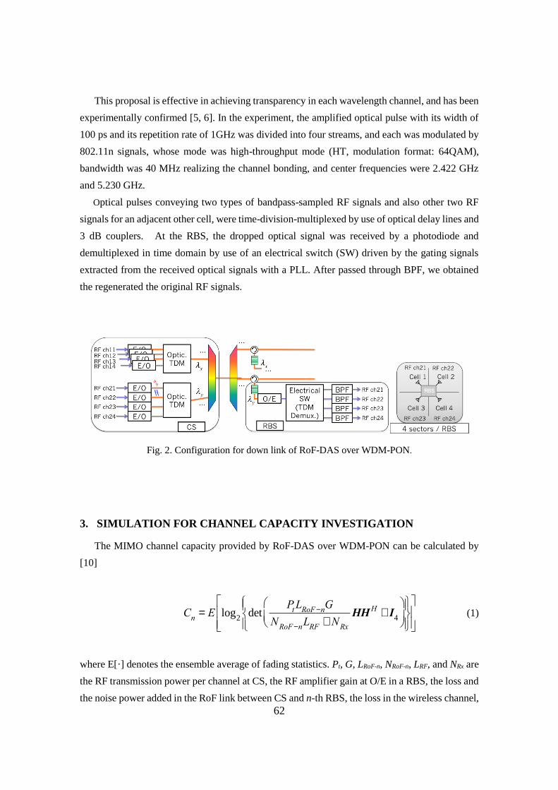
62
This proposal is effective in achieving transparency in each wavelength channel, and has been
experimentally confirmed [5, 6]. In the experiment, the amplified optical pulse with its width of
100 ps and its repetition rate of 1GHz was divided into four streams, and each was modulated by
802.11n signals, whose mode was high-throughput mode (HT, modulation format: 64QAM),
bandwidth was 40 MHz realizing the channel bonding, and center frequencies were 2.422 GHz
and 5.230 GHz.
Optical pulses conveying two types of bandpass-sampled RF signals and also other two RF
signals for an adjacent other cell, were time-division-multiplexed by use of optical delay lines and
3 dB couplers. At the RBS, the dropped optical signal was received by a photodiode and
demultiplexed in time domain by use of an electrical switch (SW) driven by the gating signals
extracted from the received optical signals with a PLL. After passed through BPF, we obtained
the regenerated the original RF signals.
Fig. 2. Configuration for down link of RoF-DAS over WDM-PON.
3. SIMULATION FOR CHANNEL CAPACITY INVESTIGATION
The MIMO channel capacity provided by RoF-DAS over WDM-PON can be calculated by
[10]
Cn
= E log2
detPtLRoF-n
G
NRoF-n
LRF
+ NRx
HHH + I
4
æ
èç
ö
ø÷
ìíï
îï
üýï
þï
é
ë
êê
ù
û
úú
(1)
where E[·] denotes the ensemble average of fading statistics. Pt, G, LRoF-n, NRoF-n, LRF, and NRx are
the RF transmission power per channel at CS, the RF amplifier gain at O/E in a RBS, the loss and
the noise power added in the RoF link between CS and n-th RBS, the loss in the wireless channel,

63
and the receiver noise power at a terminal. H and I4 are the channel matrix for wireless channel
and the 4 × 4 unit matrix. Assuming transmitting IEEE 802.11n wireless LAN signals, the
simulation selected the wireless channel matrix between the antennas of the RBSs and the mobile
terminals defined in IEEE 802.11 standard [11].
Figure 3 shows the simulation model for a radio cell configuration. We assumed 1 km width
service area. Each square cell is placed side by side. The channel capacity of each cell was
investigated as the average capacity at 25 points in a cell. The averaged channel capacity per a
small cell that was the farthest cell from CS, has been evaluated. The cell is most affected by the
transmission loss and the reflection loss generated by optical filter of each RBS. Table 1 shows
the parameters used in the simulation. Assuming the outdoor transmission, we set the boundary
distance between the LOS environment and the NLOS environment dBP to 30 m.
Fig.3. Simulation model of cell configuration.
Table 1. Parameters used in simulations.
Parameters value
RF Frequency 2.422 GHz
RF Bandwidth 40 MHz
Transmission Power per antenna 10 dBm
Height Difference between RBS and CS 10 m
Breakpoint Distance dBP 30 m
Transmitting Antenna Max Gain Gm 14 dBi
Horizontal Half-power Beamwidth HPBWh 52.5 °
Horizontal Front Back Ratio FBRh 21.25 dB
Vertical Half-power Beamwidth HPBWv 30 °
Vertical Side Lobe Level SLLv -20 dB

64
Number of antenna at a RBS / a terminal 4 / 2
Receiving Antenna Spacing 0.06 m
Receiving Antenna Gain Gr 2.14 dBi
Receiver Noise Figure 5 dB
Wireless channel model
Rician K-factor Shadow fading std.
LOS 6dB 3dB
NLOS -∞ 6dB
Figure 4 shows the channel capacity at 1st cell versus the RF SNR γT0 transmitted to the nearest
point shown in figure 3 over the RoF link [7]. The vertical dashed line shows the experimentally
obtained SNR γT0 value of 27 dB. When the SNR is low, channel capacity increases as the SNR
increases because the RoF noise link is dominant. When the SNR increases, however, the
capacity was saturated to a constant value determined by the RF transmitting power at RBS, the
wireless channel loss and the receiver noise at terminal. For smaller cell size, the saturation
value increases higher because the receiving power becomes higher.
Fig. 4. Relationship between the average channel capacity in the cell and the RF SNR transmitted
over RoF link.

65
It is observed that there is a trade-off relation between the cell size and the number of small
cell unlike conventional entrance networks for radio cells, where the smaller cell size provides
the higher channel capacity. To obtain the optimal cell size achieving the highest channel capacity,
Ref. [7] evaluated the averaged channel capacity of the whole service area and the capacity of the
farthest cell that is most affected by the accumulated loss in the WDM RoF links. Figure 5 shows
the channel capacity per a square meter versus the cell size for different conditions of radio
frequency allocation shown in figure 6. The RF SNR at the output of RoF link is assumed to be
40dB.
For all conditions, when the cell size becomes relatively small, the capacity is reduces because
of the increase of the accumulation of the reflection loss in the cascaded RoF link. When the
cell size is large, the capacity reduces as the receiver SNR at terminal decreases because of the
fixed transmitting power of 10dBm. The capacity in a large cell size corresponds to the capacity
without RoF link penalties.
Under the condition A with no interference, we can obtain the largest capacity. The optimal
cell size to achieve the highest capacity becomes approximately 100 m, but its frequency
utilization efficiency is low. Under the condition B and C, the obtained capacity are very low,
because of co-channel interference for condition B and the lower received power for condition C.
For the condition E, on the other hand, the capacity is constrained to the 70 % of that for condition
A because of co-channel interferences, but the largest capacity can be obtained at the cell size of
about 90 m with the largest radio frequency utilization efficiency.
Fig. 5. Relationship between the channel capacity and the cell size at the RoF link SNR is 40 dB.

66
Fig. 6. Conditions for radio frequency allocation.
4. CONCLUSION
This article reported the wireless channel capacity in small cells provided by RoF-DAS over
WDM-PON that can increase the capacity in a small cell with RoF entrance link and MIMO
distributed antenna. Considering the SNR of the RF signal transmitted in RoF and the
interferences among wireless cells enable results of computer simulation showed the optimized
cell size to maximize the MIMO channel capacity.
References
[1] “Heterogeneous and Small Cell Networks,” IEEE Communications Magazine, vol. 51, No.
5, May 2013.
[2] M. V. Ramkumar, A. Mihovska, N. R. Prasad, and R. Prasad, “Fuzzy-Logic Based Call
Admission Control for a Heterogeneous Radio Environment,” WPMC 2009, September 2009.
[3] J. Yu, J. Gu, X. Liu, Z. Jia, and G. Chang, “Seamless Investigation of an 8 × 2.5 Gb/s
WDM-PON and Radio-Over-Fiber Using All-Optical Up-Conversion Based on Raman-Assisted
FWM,” IEEE Photonics Technology Letters, Vol. 17, No.9, pp.1986-1988, September 2005.
[4] C. Choi, Q. Wei, T. Biermann, W. Kiess, and K. Kozu, “Mobile WDM Backhaul Network
Design for LTE-Advanced and Beyond Systems,” APMP 2012, paper FC-2, April 2012.

67
[5] T. Tashiro, K. Miyamoto, K. Hara, T. Taniguchi, J. Kani, N. Yoshimoto, K. Iwatsuki, T.
Nishiumi, T. Higashino, K. Tsukamoto, and S. Komaki, “ Broadband Ubiquitous Network Based
on RoF-DAS over WDM-PON, ”Proc. of IEEE OFC, Vol.1, No.1, pp.1-3, March 2011.
[6] K. Miyamoto, T. Tashiro, T. Higashino, K. Tsukamoto, S. Komaki, K. Hara, T. Taniguchi, J.
Kani, N. Yoshimoto and K. Iwatsuki, “Experimental Demonstration of MIMO RF Signal
Transmission in RoF-DAS over WDM-PON,” MWP 2011, paper 2122, October 2011.
[7] T. Iwakuni, K. Miyamoto, T. Higashino, K. Tsukamoto, S. Komaki, T. Tashiro, Y. Fukada, J.
Kani, N. Yoshimoto and K. Iwatsuki, “Analysis of Wireless Channel Capacity in RoF-DAS over
WDM-PON System,” IEICE Transactions on Electronics, Vol.E96-C, No.2, pp.171-179,
February 2013.
[8] T. Yamakami, et al., “An experimental investigation of applying MIMO to RoF ubiquitous
antenna system,” in Proc. IEEE Topical Meeting on MWP/APMP 2008, pp. 201-204, Sep. 2008.
[9] A. Kohlenberg, “Exact Interpolation of band-limited functions,” AIP J. of Applied Physics,
24, no.12, pp.1432-1436, Dec. 1953.
[10] G. J. Foschini, and M. J. Gans, “On Limits of Wireless Communication in a Fading
Environment When Using Multiple Antennas,” accepted for publication in Wireless Personal
Communications, Vol.6, No.3, pp.311-335, March 1998.
[11] V. Erceg, et al., “TGn Channel Models,” IEEE P802.11 Working Group for Wireless Local
Area Networks, Doc. No. IEEE802.11-03/940r4, revised 10 May 2004.
D10. Convergence of Wireless and Wired Technologies
towards Next Generation Access Networks
K. Iwatsuki
Tohoku University
ABSTRACT
The bandwidth of next generation access networks will require beyond that of current optical
access, handling the big data to download of huge data, images, and videos, as well as to upload
a large number of sensor data, anytime and anywhere. The technical convergence with wired
and wireless plays an important role to achieve the next generation access networks. In this report,
we show the perspective on next generation access networks considering the resilience against
disasters.

68
1. INTRODUCTION
Figure 1 shows the transmission speeds of core and access networks over time. The
transmission speed of optical access has increased by around 100 times in the last decade. In
order to accommodate the huge traffic from the broadband access networks, the transmission
capacities of core networks are being dramatically accelerated with the use of time-division
multiplexing (TDM), wavelength-division multiplexing (WDM), and digital coherent
technologies; so that the total transmission capacity of WDM can reach up to 6 Tbps (107 Gbps
x 640 wavelengths). As for the wireless access, the transmission speeds have also increased
more than 1Gbps with wireless LAN (IEEE 802.11ac), and accelerated up to 100Mbps mobile
access with the Long Term Evolution (LTE). We have been challenging the broadband mobile
access beyond 100Mbps with the 4G (LTE-A, LTE-B) mobile standardization, and start to the
discussion towards “Beyond 4G” (B4G).
Fig. 1. Transmission speeds of core and access networks.
On the other hand, many serious problems have become clear as a result of the East Japan
Great Earthquake, which exposed the weaknesses of the most advanced information
communications network in the world by severing the mobile phone and optical fiber lines thus
cutting off essential telecommunications services [1]. The demand for Information
Communication Technology (ICT) is summarized in Fig. 2. “Resilience,” “Green,” “Smart,”
Acce
ss ne
twork
Core ne
twork
1.6G
2.4G
400M
10G
TDM
WDM
40G
Ethernet
100BASE- T
10GbE
10BASE- T
100GbE
40Gx80
10Gx80
10Gx48
GbE
107Gx640
Digital coherenttechnology 10T
1T
100G
10G
1G
1980 1985 1990 1995 2000 2005
Year
Bit
rate
(bps)
2010 2020
10M
1M
Wired and Wireless
convergence
STM- PON
B- PON
G- EPON
10G- EPON
3G( HSDPA)
LTE
4G
Optical
Access
802.11a
802.11b
802.11g
802.11n
Wireless
LAN
WDM- PON
Mobile
100M
B4G
802.11ac
Next Generation Access
WiGig

69
and “Secure” of and/or by the ICT are strongly required after we experienced the Great
Earthquake. To achieve these requirements to the ICT, access networks will have flexibility to
accommodate not only high speed but also low speed wireless interfaces as shown in Fig. 3.
In this report, we describe the perspective on next generation access networks considering the
resilient ICT.
Fig. 2. Demand for ICT.
Fig. 3. Various wireless interface.
3G1M
10k
1k
100k
10M
100M
1G
Data
rate
(bps)
MobilityStationary Quasi-stationary Walking speed Vehicle speed
Zig-Bee
4G( LTE-A, LTE-B)
Wi-Fi
WiMAX LTE
10GB4G
Primary industries
ITS
Smart city
Secondary industries
WiGig
Ultra-high speed WiFi
PROFINET
Operator
Society Industry
Productivityimprovement
Resilient
Secure
Green
Open
Broadband
Ubiquitous
Smart
Standardization
Cost reduction
User
Globalization
Environmentalprotection
Disasterprevention
Safety
Service innovation
Convenience
Reduction ofCAPEX and OPEX

70
2. NEXT GENERATION ACCESS NETWORK
2.1. Concept of next generation access network
The concept of next generation access network in Fig. 4 shows the four orientations;
broadband ubiquitous, green, resilient, cost reduction. These orientations of access network are
realized with the following approaches.
(1) Broadband ubiquitous access networks will be achieved with introducing multilayer and
small-cell architecture using high radio frequency.
(2) Green access networks will be achieved with simultaneously controlling the multilayered
wireless networks, such as 3G, LTE, 4G, and B4G, according to the traffic distribution in service
area.
(3) Resilient access networks will be achieved to be complimented by wired and wireless network
each other and/or to introduce multilayered wireless network architecture.
(4) Construction cost of access networks will be reduced with sharing the transmission line and
transceivers with many users, and with introducing the transceivers commonly used as wired and
wireless, which are made by common components widely used in opt-electronics industries.
Fig. 4. Concept of next generation access network.
2.2. Optical backhaul
Figure 5 shows multilayered wireless access network with optical backhaul to achieve the
above concept. The 3G service covers the large cell, which includes LTE, 4G, and B4G service
areas, respectively, so that we call the multilayered wireless access network. The optical
backhaul to accommodate LTE services is single star architecture. In order to accommodate 4G
v Cloud control v Complement
v Sharev Common
v Small cellv High RF
v multilayer
Next generationAccess network
Broadband
Ubiquitous
Resilient
Cost
reduction
Gree
n

71
and B4G services, we will apply PON architecture to the optical backhaul to reduce the cost.
The 3G networks can be adopted control plain of LTE, 4G, and B4G networks as well. We can
also accommodate sensor networks with the control plain of 3G networks.
We summarize the WDM access networks based on PON architecture in Fig. 6. These access
networks are applied to the optical backhaul of multilayered wireless access network. The 3G
and 4G services are supported with Coarse WDM (CWDM)-PON and Dense WDM (DWDM)-
PON, respectively. We will provide B4G service with a distributed antenna network (DAN)
with femto-cell architecture. We have proposed the radio over fiber (RoF) DAN over Super
DWDM (SDWDM)-PON [2] to combine WDM access [3] and a DAN with multiple input
multiple output (MIMO) technologies [4]. The provision of various wireless services per
wavelength in WDM access can be accommodated. The WDM access will achieve the
flexibility for non-uniform traffic distribution and the user-mobility in various wireless services.
Fig. 5. Multilayered wireless access network with optical backhaul.
Sensornetwork
B4G LTE
4G
3G
Carrier housing
FTTH
ONU
WiFi/WiGig
PON
PON
Long reach PON
Sensornetwork
Carrierhousing
Carrierhousing
Hig
h s
peed a
nd larg
e c
apacity
Distributed Antenna Network
Wireless over DWDM- PON
GE-ONU
λ 1-ONU
λ 2-ONU
ONU
ONU
GE-OLT
λ 1-OLT
λ 2-OLT
OLT
OLT
DWDM-PON
BS
YearWireless over CWDM- PON
ONU
λ 2-OLT
λ 2-OLT
λ 2-OLT
CWDM-PON
BS
ONU
ONU
FTTH
B4G
4G
SDWDM-PON
4G
〜2020〜2000
3G
ONU
BS
3G

72
Fig. 6. Evolution of WDM access network.
2.3. Configuration of RoF-DAN over WDM-PON
In this section, we introduce the proposed RoF-DAN over WDM-PON. Figure 7(a)
illustrates a configuration of WDM-PON, where two wavelengths are assigned to each BS as an
up- and down-stream. We employ a 2 x N arrayed waveguide gratings (AWGs) as a wavelength
multi/demultiplexer, to achieve a low dissipation for accommodating a large number of BSs in
single feeder fibers. At the CS, four MIMO RF signals for different four cells are multiplexed
in the MIMO signal processing in Fig. 7(a). Each BS consists of an optical circulator without
any wavelength selectivity to make it easy to add upstream signals and drop downstream signals.
Optical filters, such as fiber gratings, at the BS are used to select a wavelength assigned to the BS.
This configuration achieves the transparency of transmission lines through its lack of optical
filters, and thus has scalability of upgrading wavelength channels in the future. To decrease the
costs of operation, administration, and maintenance functions, as well as the production cost, we
can introduce wavelength tunability in LDs and fiber gratings of BSs; that is colorless BS [4].
Figure 7(b) illustrates wavelength allocation for upstream and downstream. By using cyclic
property of AWG, the wavelength of upstream are shifted with one wavelength against those of
downstream. We require N + 1 wavelengths to accommodate N BSs over the WDM-PON, thus
lead to enhancing the wavelength utilization.
Fig. 7(a). Configuration of WDM-PON.
Cell
BS BS BS BS
BS BS BS BS
BS BS BS BS
BS BS BS BS
BS BS BS BS
MIMO
CS
Downstream
Upstream
BSTx
Rx
Fiber
grating
Circulator
CS
2xN AWG
One
wavelength
shift
RxRx
Rx
・・・
TxTx
Tx
・・・
MIMOsignal
processing
RFRF
RF
・・・
MIMOsignal
processing
RFRF
RF
・・・
11 22 33 44
Fiber 1
Fiber 2
Fiber 3
Fiber 4
Fiber 5
Optical branch
Cell
BS BS BS BSBS BS BS BS
BS BS BS BSBS BS BS BS
BS BS BS BSBS BS BS BS
BS BS BS BSBS BS BS BS
BS BS BS BSBS BS BS BS
MIMO
CS
Downstream
Upstream
BSTx
Rx
Fiber
grating
Circulator
CS
2xN AWG
One
wavelength
shift
RxRx
Rx
・・・
TxTx
Tx
・・・
MIMOsignal
processing
RFRF
RF
・・・
MIMOsignal
processing
RFRF
RF
・・・
11 22 33 44
Fiber 1
Fiber 2
Fiber 3
Fiber 4
Fiber 5
Optical branch
Wavelength allocation in fiber 1
Transmission characteristic of fiber
grating
Wavelength
Wavelength
1
upstream
2 3 4
11
downstream
22 33 44
Wavelength
Wavelength allocation for up- and down-stream
One wavelength shift
with 2xN AWG
Wavelength allocation in fiber 1
Transmission characteristic of fiber
grating
Wavelength
Wavelength
1
upstream
2 3 4
11
downstream
22 33 44
Wavelength
Wavelength allocation for up- and down-stream
One wavelength shift
with 2xN AWG

73
Fig. 7(b). Wavelength allocation of WDM-PON.
2.4. Experimental results of RoF-DAN over WDM-PON
Figure 8 shows our experimental setup to transmit downstream signals of RoF-DAN over
WDM-PON with optical TDM and the signal transition diagram at each component [5]. We
assumed that 2 x 2 MIMO signal transmission in a cell as shown in Fig.2. Two wavelengths
were used to realize 2 x 2 MIMO signal transmission; two 802.11n RF signals in the 2.4 and 5
GHz bands were multiplexed in each wavelength with optical TDM and transmitted to the BS.
The two continuous lightwaves emitted from DFB-LDs were wavelength-multiplexed in Fig.
8 (a), and modulated with a lithium niobate Mach-Zehnder modulator (LN-MZM) driven with a
return to zero (RZ) pulse of 100 ps pulse width at a 1 GHz repetition rate from a pulse pattern
generator (PPG) in Fig. 8 (b). Two wavelength signals were amplified with an erbium doped
fiber amplifier (EDFA) and demultiplexed with an AWG of 25 GHz wavelength spacing. Each
wavelength was divided with a 3 dB coupler and modulated with each LN-MZM driven by
802.11n RF signals with 40 MHz bandwidth whose center frequencies were 2.422 GHz (ch 3)
and 5.230 GHz (ch 46) from the vector signal generator (VSG) in Fig. 8 (c). At the output of
each LN-MZM, we obtained the bandpass-sampled RF signals of the 2.4 and 5 GHz bands. The
modulation and coding scheme (MCS) index of 802.11n RF signals was 15 [6] i.e. 64-quadrature
amplitude modulation (QAM) orthogonal frequency division multiplexing (OFDM) signals.
We employed optical delay lines and 3 dB couplers to optically multiplex the bandpass-sampled
RF signals and dummy RF signals of an adjacent cell, as shown in Fig. 8 (d). The optically
multiplexed RF signals were wavelength-multiplexed again and transmitted through the optical
feeder fiber as a downstream signal.
The transmitted signals from the CS were distributed to each BS with the AWG, and the
wavelength assigned at the BS was dropped by the 3-port circulator. The downstream signal
dropped at the BS was converted by the photo diode transimpedance amplifier (PD-TIA), and
demultiplexed with a high-speed electrical switch (SW) in Fig. 8 (f). The SW was driven by a
control signal with a 300 ps pulse width at 1 GHz repetition rate from the PPG. The
demultiplexed RF signals were converted to original RF signals with the band pass filter (BPF),
which were transmitted as wireless signals from antennas at BS in Fig. 8 (g).

74
Fig. 8. Experimental setup and signal transition diagram.
Firstly, we performed back-to-back transmission using one wavelength, namely D1 signal to
evaluate the performance of TDM and RF signal transmission as shown in Fig. 8. We evaluated
the waveforms of time division multiplexed/demultiplexed RF signals and the constellations and
error vector magnitude (EVM) value of 64-QAM OFDM signals at the BS by the vector signal
analyzer (VSA).
The experimental results from (i) to (v) in Fig. 9 correspond to the measured points at the
experimental setup in Fig. 8. To evaluate the TDM performance, we transmitted the optical pulse
train without the RF modulation. Figure 9 (i) shows a transmitted optical pulse train from the
CS, and Fig. 9 (ii) and (iii) show the demultiplexed electrical signals with the SW in BS. It
clearly shows the good performance of TDM operation in the experimental setup. To evaluate
the performance of transmitted RF signals, we modulated the optical pulse train with the RF
signals. Figure 9 (iv) and (v) show the analyzed 2.4 and 5 GHz band RF signals after the BPF,
(ii)
(iii)
ANT1
ANT2
D1
D2
(i)
From feeder fiber
Synchronized with BS
To feeder fiber
Delay
Delay
Delay
Delay
DFB-LD
DFB-LD
LN-MZM
PC
PC
PC
PC
1GHz100ps widthRZ pulse
LN-MZM
D2
D1
Delay
Center Station (Tx)
Delay
EDFA EDFALN-MZM
VSG(2.4/5GHz)
AWG
PC
1552.524 nm(193.1 THz)
1553.329 nm(193 THz)
VSG(2.4/5GHz)
LN-MZM
LN-MZM
FadingSimulator
10G PPG
VOAUpstream port
BPF
BPF
2.4 GHz
5 GHz
Base Station 1 (Rx)
10G PPG
PD-TIA(O/E)
D2
D1
Cont.
Synchronizedwith CS
ANT1
ANT1
VOAUpstream port
BPF
BPF
2.4 GHz
5 GHz10G PPG
PD-TIA(O/E)
Cont.
ANT2
ANT2
Base Station 2 (Rx)
VSA(2.4GHz/5GHz)
SW
SW
D1
100ps
1000pst
D2
2.4 GHz ANT1
5 GHz ANT1
2.4 GHz ANT2
5 GHz ANT2
Dummy signalsfor adjacent cell
t
t
t
t
t
t
t t
t
t
CWlightwave
RZ pulse modulated
(Bandpass-sampling)
t
t
t
t
SuperimposedRF signals
Dummy signal generation and OTDM
1000ps
Objective cell Adjacent cell
1000ps
t
t
Objective cell Adjacent cell
Transmitted opticalWDM/OTDM signals
(a) (b) (c) (d) (e)
t
t2.4 GHz ANT1
t2.4 GHz ANT2
t5 GHz ANT1
t5 GHz ANT2
t
t
t
t
Time divisiondemultiplexing
RF signal regenerationand transmission over air
(f) (g)
(a)
(b)
(c)(d)
(e)
(f) (g)
(iv)
(v)(ii)
(iii)
ANT1
ANT2
D1
D2
(i)
From feeder fiber
Synchronized with BS
To feeder fiber
Delay
Delay
Delay
Delay
DFB-LD
DFB-LD
LN-MZM
PC
PC
PC
PC
1GHz100ps widthRZ pulse
LN-MZM
D2
D1
Delay
Center Station (Tx)
Delay
EDFA EDFALN-MZM
VSG(2.4/5GHz)
AWG
PC
1552.524 nm(193.1 THz)
1553.329 nm(193 THz)
VSG(2.4/5GHz)
LN-MZM
LN-MZM
FadingSimulator
10G PPG
VOAUpstream port
BPF
BPF
2.4 GHz
5 GHz
Base Station 1 (Rx)
10G PPG
PD-TIA(O/E)
D2
D1
Cont.
Synchronizedwith CS
ANT1
ANT1
VOAUpstream port
BPF
BPF
2.4 GHz
5 GHz10G PPG
PD-TIA(O/E)
Cont.
ANT2
ANT2
Base Station 2 (Rx)
VSA(2.4GHz/5GHz)
SW
SW
D1
100ps
1000pst
D2
2.4 GHz ANT1
5 GHz ANT1
2.4 GHz ANT2
5 GHz ANT2
Dummy signalsfor adjacent cell
t
t
t
t
t
t
t t
t
t
CWlightwave
RZ pulse modulated
(Bandpass-sampling)
t
t
t
t
SuperimposedRF signals
Dummy signal generation and OTDM
1000ps
Objective cell Adjacent cell
1000ps
t
t
Objective cell Adjacent cell
Transmitted opticalWDM/OTDM signals
(a) (b) (c) (d) (e)
t
D1
100ps
1000pstt
D2
2.4 GHz ANT1
5 GHz ANT1
2.4 GHz ANT2
5 GHz ANT2
Dummy signalsfor adjacent cell
tt
tt
tt
tt
tt
tt
tt tt
tt
tt
CWlightwave
RZ pulse modulated
(Bandpass-sampling)
tt
tt
tt
tt
SuperimposedRF signals
Dummy signal generation and OTDM
1000ps
Objective cell Adjacent cell
1000ps
tt
tt
Objective cell Adjacent cell
Transmitted opticalWDM/OTDM signals
(a) (b) (c) (d) (e)
tt
t2.4 GHz ANT1
t2.4 GHz ANT2
t5 GHz ANT1
t5 GHz ANT2
t
t
t
t
Time divisiondemultiplexing
RF signal regenerationand transmission over air
(f) (g)
t2.4 GHz ANT1
t2.4 GHz ANT2
t5 GHz ANT1
t5 GHz ANT2
tt
tt
tt
tt
Time divisiondemultiplexing
RF signal regenerationand transmission over air
(f) (g)
(a)
(b)
(c)(d)
(e)
(f) (g)
(iv)
(v)

75
respectively. The EVM values of -26.0 and -23.2 dB were obtained, respectively. The optical
powers at the PD-TIA input and the electrical powers at the VSG output were -3 and 5 dBm for
Fig. 9(iv) and -3 and 10 dBm for Fig. 9(v), respectively.
Fig. 9. Experimental results. (i) OTDM signal, (ii) and (iii) demultiplexed signals, (iv) constellation
of 2.4 GHz band transmitted RF signal, (v) constellation of 5 GHz band transmitted RF signal.
Next, we performed back-to-back MIMO RF signal transmission using two wavelengths D1
and D2. The Fading simulator employed before VSG generated 2 x 2 MIMO transmission of
2.4 GHz band RF signals under the Rayleigh fading model, in which the number of path, the delay
between the paths, and the difference of loss between the paths were 2, 0.11 ns, and 8 dB,
respectively. Figure 10(a) and (b) show the analyzed RF signals of D1 and D2 without the
multipath fading, respectively. The EVM values of -26.5 and -24.1 dB were obtained,
respectively, which are almost the same values of Fig. 9(iv). The optical powers at the PD-TIA
input and the electrical powers at the VSG output were -1 and 8 dBm for both D1 and D2,
respectively. Figure 10(c) and (d) depict the RF spectrum of D1 and D2, which clearly show
the 802.11n RF signals of 40MHz bandwidth. These results lead to the good performance of
WDM and TDM operation. To evaluate the performance of transmitted 2.4 GHz band RF
signals with multipath fading, we operated the fading simulator. Figure 11(a) and (b) show the
analyzed RF signals of D1 and D2, respectively. The EVM values of -22.7 and -21.9 dB were
obtained, respectively. The optical powers at the PD-TIA input and the electrical powers at the
VSG output were the same values without the multipath fading. Figure 11(c) and (d) depict the
RF spectrum of D1 and D2, in which the frequency selective fading due to the fading simulator
is still alive. The experimental results confirm the basic feasibility of optical TDM and
bandpass-sampled MIMO RF signal transmission in the proposed RoF-DAN over WDM-PON
architecture.
100 psGuardtime
150 ps
2.4 GHz 2.4 GHz(Dummy)
5 GHz 5 GHz(Dummy)
40 mV
2.4 GHz bandconstellation
EVM : -26.0 dB
5 GHz bandconstellation
EVM : -23.2 dB
(i)
(iv) (v)
100 ps
2.4 GHz 2.4 GHz(Dummy)
5 GHz
(ii)
5 GHz(Dummy)
40 mV
100 ps
2.4 GHz 2.4 GHz(Dummy)
5 GHz
(iii)
5 GHz(Dummy)
100 psGuardtime
150 ps
2.4 GHz 2.4 GHz(Dummy)
5 GHz 5 GHz(Dummy)
40 mV
2.4 GHz bandconstellation
EVM : -26.0 dB
5 GHz bandconstellation
EVM : -23.2 dB
(i)
(iv) (v)
100 ps
2.4 GHz 2.4 GHz(Dummy)
5 GHz
(ii)
5 GHz(Dummy)
40 mV
100 ps
2.4 GHz 2.4 GHz(Dummy)
5 GHz
(iii)
5 GHz(Dummy)

76
Fig. 10. Experimental results of MIMO RF signal transmission without multipath fading. (a) and (b)
constellation of 2.4 GHz band transmitted RF signal in D1 and D2, respectively. (c) and (d) 2.4
GHz band transmitted RF spectrum in D1 and D2, respectively.
Fig. 11. Experimental results of MIMO RF signal transmission with multipath fading. (a) and (b)
constellation of 2.4 GHz band transmitted RF signal in D1 and D2, respectively. (c) and (d) 2.4
GHz band transmitted RF spectrum in D1 and D2, respectively.
3. RESILIENT NETWORKS
The recent progress of cloud computing needs to easily connect to the big data with smart
phones and tablet personal computers anywhere, at any time, with the multilayered wireless
access network and sensor network. These networks forms the infrastructure for smart house,
smart city, disaster prevention, remote medical care, health care, and so on, as shown in Fig. 12,
and therefore we have to realize the resilience of and/or by the network in Fig. 5. A cloud radio
2.4 GHz bandλD1 constellation
EVM : -25.6 dB
2.4GHz bandλD2 constellation
EVM : -24.1 dB
2.4 GHz bandλD1 spectrum
2.4 GHz bandλD2 spectrum
(a) (b)
(c) (d)
2.4 GHz bandλD1 constellation
EVM : -25.6 dB
2.4GHz bandλD2 constellation
EVM : -24.1 dB
2.4 GHz bandλD1 spectrum
2.4 GHz bandλD2 spectrum
(a) (b)
(c) (d)
2.4 GHz bandchannel1 constellation
EVM : -22.7 dB
2.4GHz bandchannel2 constellation
EVM : -21.9 dB
2.4 GHz bandchannel1 spectrum
2.4 GHz bandchannel2 spectrum
(a) (b)
(c) (d)
2.4 GHz bandchannel1 constellation
EVM : -22.7 dB
2.4GHz bandchannel2 constellation
EVM : -21.9 dB
2.4 GHz bandchannel1 spectrum
2.4 GHz bandchannel2 spectrum
(a) (b)
(c) (d)

77
access network (C-RAN) in Fig. 12 is the most promising approach to control the multilayered
wireless networks to achieve the resilience in the disasters as well as the energy saving in usual
according to the traffic distribution in the wireless service area.
Fig. 12. Whole picture of resilient network.
Figure 13 shows the conceptual structure of multilayered communications network, which is
to establish an alternative communication route and to develop its related technologies [7]. In
case of a disaster, the commercial operator’s cellular network may fall into severe traffic
congestion or is damaged. When this happens, a mobile phone will automatically connect to a
surviving local network, which will be private Wi-Fi, WiMAX, dedicated networks such as cable,
satellite, and ITS (Intelligent Transportation Systems) networks. To enable such an autonomous
network selection, a “Policy server” will be installed in each network. The policy server
monitors its own network and decides whether or not the network can be open to third users based
on its own network policy. Accordingly, a new function needs to be installed on mobile phones
to select and access to one of the local networks. The decision is made with monitoring its
surrounding radio environment and information broadcasted from the policy server in each
network.
4. SUMMARY
We have described the perspective on next generation access networks taking into account of
Access network
Core network
Cloud computing
ONU
LTE 4G
ONU: Optical Network Unit
FTTH
BS BS BS
BS: Base station
ONU
Sensor network
Sensor network
ITS
Sensor network
Big data
HEMS
CEMS BEMS
EV
EHR
C-RAN (Cloud-RAN)
B4G
3G
WiFi/WiGig
Sensor network Sensor network
Smart city Health care
Smart house
Ultra-high Speed WiFi
Disaster prevention
Remote medical care
Watch
ICT Unit Mobile Ad- hoc network

78
the resilience ICT. The four orientations; broadband ubiquitous, green, resilient, cost reduction,
were proposed as the concept of next generation access network. The multilayered wireless
access network with optical backhaul based on WDM access was addressed as one of the most
promising architecture to realize the concept.
Fig. 13. Conceptual structure of multilayered communications network.
References
[1] K. Iwatsuki, “The projects of disaster-resistant information communication network at the
Research Organization of Electrical Communication, Tohoku University,” Proc. of SPIE,
Vol.8646, No.86460B, invited paper, SPIE Photonics West 2013, 2013.
[2] K. Tsukamoto, T. Nishiumi, T. Yamagami, T. Higashino, S. Komaki, R. Kubo, T. Taniguchi,
J. Kani, N. Yoshimoto, H. Kimura, and K. Iwatsuki, “Convergence of WDM access and
ubiquitous antenna architecture for broadband wireless services,” Progress In Electromagnetics
Research Symposium (PIERS) 2010, 2010.
[3] K. Iwatsuki, J. Kani, H. Suzuki, and M. Fujiwara, “Access and Metro Networks based on
WDM Technologies,” IEEE J. Lightwave Technol., Vol. 22, No.11, pp.2623-2630, 2004.
[4] S. Okamura, M. Okada, K. Tsukamoto, S. Komaki, H. Yamamoto, “Impact of successive
interference canceller on the performance of ubiquitous antenna-based SDMA system,”

79
Electronics and Communications in Japan, Part 3 (Fundamental Electronic Science), Vol.1, No.3,
pp.10-24, 2004.
[5] T. Tashiro, K. Miyamoto, K. Hara, T. Taniguchi, J. Kani, N. Yoshimoto, K. Iwatsuki, T.
Nishiumi, T. Higashino, K. Tsukamoto, S. Komaki, “Broadband ubiquitous network based on
RoF-DAS over WDM-PON,” OFC’2011, 2011.
[6] IEEE Std 802.11n-2009.
[7] F. Adachi, “Disaster-resilient multilayered communications network,” Panel 1: Japan National
Project: Creation of Disaster-resilient Networks, IEEE PIMRC 2012, 2012.
D11. Optical Access Technologies for Mobile Fronthaul
J. Kani
NTT
1. INTRODUCTION
The deployment of Long Term Evolution (LTE) is rapidly spreading, and its upgrade to LTE-
Advanced has already been standardized [1]. While LTE provides the peak rate of 300 Mbit/s
downstream and 75 Mbit/s upstream, LTE-Advanced extends these to 1 Gbit/s downstream and
500 Mbit/s upstream. To support the explosion in mobile broadband traffic [2], further
enhancement of the mobile broadband systems is under study in 3GPP [3].
To provide higher bandwidth in wireless/mobile systems, we generally need to decrease the
cell size. The need to accommodate many more antennas, and the higher speeds involved,
emphasizes the importance of cost-effective optical access technologies such as Passive Optical
Network (PON) systems [4]. This part of the report summarizes recent progress in optical access
technologies for supporting wireless/mobile systems.
2. C-RAN AND FRONTHAUL INTERFACES
In mobile networks, the base-station (BS) equipment, called eNodeB in LTE and LTE-
Advanced, comprises two parts: one is Base Band Unit (BBU) for digital baseband processing
and the other is Radio Equipment (RE) for transmitting and receiving wireless signals. RE can
be replaced by Remote Radio Head (RRH) for realizing the centralized radio access network (C-
RAN) architecture shown in Figure 1. The optical segment, i.e. between BBU and RRH in this
architecture, is now called “mobile fronthaul”.

80
Fig. 1. C-RAN architecture.
A popular interface for connecting BBU and RRH is Common Public Radio Interface (CPRI)
[5]. Based on CPRI, European Telecommunications Standards Institute (ETSI) is specifying
Open Radio Equipment Interface (ORI) [6]. Such interfaces are called “fronthaul interfaces” in
this report. The fronthaul interfaces carry digitized (i.e. IQ-sampled) radio components and so
require very broad bandwidth, i.e. bandwidth of the order of the product of IQ sampling rate and
quantization bit rate [7]. They also require very low latency and latency jitter to avoid interfering
with the hybrid automatic repeat request (HARQ) procedure between BBU and user equipment
(UE) [7].
The C-RAN architecture decreases equipment size and cost at the antenna points as well as
realizing Coordinated Multi-point transmission/reception (CoMP), introduced in LTE-Advanced
to increase the cell-average and cell-edge throughput, in a simple and effective manner [8].
Technologies to construct a practical C-RAN infrastructure such as multiplexing and compression
techniques have been emerging in the last few years.
3. MULTIPLEXING AND COMPRESSION TECHNIQUES
One of the techniques to multiplex the fronthaul signals is wavelength-division multiplexing
(WDM): an example configuration is illustrated in Figure 2. As shown in the figure, multiple
CPRI links, e.g. for multiple antennas and multiple frequency bands, are transmitted over a single
fiber by the use of WDM: each the fronthaul-interface signal uses a different wavelength pair.
Additional delay and jitter are negligible because the multi/demultiplexing is done with a passive
optical device such as an arrayed waveguide grating (AWG).
RRH
RRH
RRH
RRH
BBU
Optical link Base Station

81
Fig. 2. WDM for fronthaul signals.
Another technique is CPRI over OTN defined by ITU-T. CPRI can be accommodated in
OTN through the use of mapping procedures for Constant Bit Rate (CBR) signals defined in ITU-
T G.709. Some careful consideration is needed as regards the jitter as described in Appendix
VIII of ITU-T G.709.
Because the bandwidth of CPRI/ORI will become huge as mentioned above, CPRI
compression techniques are being extensively researched [9, 10]. ORI compression is under
study in ETSI. Network operators will be able to construct the C-RAN infrastructure by
selecting and combining the multiplexing and compression techniques of the fronthaul interfaces
in an effective manner.
4. MOBILE FRONTHAUL BASED ON PON
To provide higher bandwidth in wireless/mobile systems, we generally need to decrease the
cell size, i.e. to densely set small cells. The point-to-multipoint optical access technology, i.e.
PON technology, is very effective for such densely located small cells because a single optical
fiber can be effectively shared among many RRHs as illustrated in Figure 3. There have been
several studies to construct the mobile fronthaul with PON technology [9, 11, 12].
Currently standardized PON systems, such as ITU-T G-PON and XG-PON as well as IEEE
1G-EPON and 10G-EPON, are based on time-division multiplexing and time-division multiple
access (TDM/TDMA). The TDM/TDMA PON technique enables multiple, e.g. 8 to 64, optical
network units (ONUs) located in subscribers’ home to share a single optical fiber via an optical
splitter as well as to share the optical line terminal (OLT) including an optical transceiver located
in the central office (CO), thus realizing a very economic system. However, the latency caused
by the dynamic bandwidth allocation (DBA) becomes a problem when applying the TDM/TDMA
PON to the mobile fronthaul. Recently, a novel bandwidth allocation scheme to address this has
been reported [11]. The combination of TDM/TDMA PON with the adaptive compression
method is very effective for constructing the mobile fronthaul for the radio access networks with
n
1
……
BBU
RRHOptical fiber
n
1
Wavelengthmux/demux(e.g. AWG)
Opticaltransceivers
RRH
Opticaltransceivers
Wavelengthmux/demux(e.g. AWG)

82
densely set small cells [9].
(a) (b)
Fig. 3. Fronthaul architecture with (a) point-to-point fiber connections, and (2) PON configuration.
Another approach is to apply WDM-PON, in which each RRH is connected to BBU with a
different wavelength pair [12]. Further studies will be done in the industry to compare the
TDM/TDMA-PON and the WDM-PON in terms of cost and performance. ITU-T is
standardizing the second next-generation PON (NG-PON2) as G.989 series. The NG-PON2
system adopts the combination of TDM/TDMA and WDM, so it will be possible to flexibly
allocate the timeslot and wavelength resources to construct the mobile fronthaul depending on the
requirement.
To further extend the mobile fronthaul architecture and increase the performance of small-
cell networks, the Distributed Antenna System (DAS) is an interesting approach: Figure 4 shows
a general schematic of DAS over a PON system. In DAS, each cell is surrounded by several
antennas rather than putting an antenna at the center of the cell. Base stations (BSs) are
connected to the central station (CS), which performs all signal processing. This configuration
improves the performance of wireless communication by providing diversity gain; the bandwidth
is readily increased by the use of multi-input multi-output (MIMO).
It is very reasonable to apply a PON system between BSs and CS in DAS, especially when
the cell size is relatively small and the number of BSs is large because otherwise we would need
a lot of optical fibers between BSs and CS.
One question is how to multiplex the signals to/from BS antennas. A DAS over WDM-PON
technique has been proposed, in which radio-frequency signals from antennas are bandpass-
sampled and multiplexed in the time domain in each BS and WDM is used to multiplex BS-to-
CS signals [13, 14].
RRH RRH
RRHRRH
BBU
RRH RRH
RRHRRH
BBU
Optical fibersOptical fiber
Optical splitter

83
Fig. 4. Distributed Antenna System (DAS) over PON.
References
[1] T. Nakamura, S. Abeta, H. Takahashi, S. Nagata, “Advanced Technologies in LTE/LTE-
Advanced,” NTT DOCOMO Technical Journal, Vol. 15, No.2, pp. 4-8, 2013.
[2] Cisco Visual Networking Index (VNI), 2013.
[3] http://www.3gpp.org/
[4] J. Kani, F. Bourgart, A. Cui, A. Rafel, M. Campbell, R. Davey, S. Rodrigues, “Next-generation
PON-part I: Technology roadmap and general requirements,” IEEE Commun. Mag., Vol. 47,
Issue 11, pp. 42-49, 2009.
[5] Common Public Radio Interface; http://www.cpri.info/
[6]http://www.etsi.org/images/files/ETSITechnologyLeaflets/OpenRadioEquipmentInterface.pd
f
[7] Thomas Pfeiffer, “OPTICAL ARCHITECTURES FOR MOBILE BACK- AND
FRONTHAULING,” OFC/NFOEC wireless backhauling workshop - Los Angeles, 5.3.2012.
[8] D. Lee, H. Seo, B. Clerckx, E. Hardouin, D. Mazzarese, S. Nagata, K. Sayana, “Coordinated
multipoint transmission and reception in LTE-advanced: deployment scenarios and operational
challenges,” IEEE Commun. Mag. Vol. 50, Issue 2, pp. 148-155, 2012.
[9] N. Shibata, S. Kuwano, J. Terada, and N. Yoshimoto, “Data Bandwidth Reduction based on
Wireless Resource Allocation for Digitized Radio over TDM-PON System,” in Optical Fiber
Communication Conference/National Fiber Optic Engineers Conference 2013, OSA Technical
Digest (Optical Society of America, 2013), paper OTh4A.6.
[10] S. Nanba, A. Agata, “A new IQ data compression scheme for front-haul link in Centralized
RAN,” 2013 IEEE 24th International Symposium on Personal, Indoor and Mobile Radio
Communications (PIMRC Workshops), pp. 210-214, 2013.
BS BS BS BS
BS BS BS BS
BS BS BS BS
BS BS BS BS
CS
Optical splitter or
wavelength router

84
[11] G. Yazawa, T. Tashiro, S. Kuwano, J. Terada, N. Yoshimoto, “Low-latency transmission
technique for mobile fronthaul based on TDM-PON,” IEICE Society Conference 2013,
Communication (2), 181, 2013 (in Japanese).
[12] Y. Horiuchi, “Economical Solutions of the WDM-PON System,” in Optical Fiber
Communication Conference, OSA Technical Digest (Optical Society of America, 2012), paper
OW3B.6, 2012.
[13] T. Tashiro, H. Hara, J. Kani, N. Yoshimoto, K. Iwatsuki, K. Miyamoto, T. Nishiumi, T.
Higashino, K. Tsukamoto, and S. Komaki, “Experimental demonstration of RoF-DAS over
WDM-PON with bandpass-sampling and optical TDM techniques,” IEICE Electron. Exp., vol. 9,
no. 3, pp. 206–212, Feb. 2012.
[14] K. Miyamoto, T. Tashiro, Y. Fukada, J. Kani, J. Terada, N. Yoshimoto, T. Iwakuni, T.
Higashino, K. Tsukamoto, S. Komaki, K. Iwatsuki, “Transmission Performance Investigation of
RF Signal in RoF-DAS Over WDM-PON With Bandpass-Sampling and Optical TDM,” J.
Lightwave Technol. 31, 3477-3488, 2013.