Embed Size (px)
Citation preview

1
Combined FRM and GDFT filter bank
designs for improved non-uniform DSA
channelization
Álvaro Palomo-Navarro, Ronan J. Farrell, Rudi Villing
Callan Institute for Applied ICT, Electronic Engineering Department,
National University of Ireland Maynooth, Maynooth, Co. Kildare, Ireland
Email: {apalomo, ronan.farrell, rudi.villing}@eeng.nuim.ie
ABSTRACT
Multi-standard channelization for base stations is a big application of Generalised Discrete Fourier
Transform Modulated Filter Banks (GDFT-FB) in digital communications. For technologies such as
Software-Defined Radio (SDR) and Cognitive Radio (CR), non-uniform channelizers must be used if
frequency bands are shared by different standards. However, GDFT-FB based non-uniform channelizers can
suffer from high filter orders when applied to wideband input signals. In this paper various combinations of
GDFT-FB with the Frequency Response Masking (FRM) technique are proposed and evaluated for both
uniform and non-uniform channelization applications. Results show that the proposed techniques achieve
savings in both the number of filter coefficients and the number of operations per input sample.
KEYWORDS
Frequency response masking; generalised discrete Fourier transform modulated filter banks; uniform
channelization; non-uniform channelization; dynamic spectrum allocation.
I. INTRODUCTION
Modulated filter banks have gained importance in digital communications because of
their application to multi-carrier modulation techniques and channelizers for base stations
[1, 2]. In the latter application, channelization implies the extraction of independent
channels contained in the received uplink signal by bandpass filtering and down-converting
them prior to subsequent baseband processing of each channel independently. Modulated
filter banks eliminate the need for an independent low-pass or band-pass filter to isolate

2
each information channel, replacing them with a single low-pass prototype filter and an
efficient modulation operation that can filter multiple channels at once. As a result, the
computational load of the channelization is shared among multiple channels, and does not
increase linearly with the number of channels.
Recent trends in wireless communications such as Software-Defined Radio (SDR) [3]
and Cognitive Radio (CR) [4] make use of Dynamic Spectrum Allocation (DSA)
techniques to make more efficient use of the radio communications spectrum [5, 6]. With
DSA the same frequency band may be shared by different wireless standards with different
channel properties. Some of the advantages of DSA are an efficient utilisation of some
frequency bands, better electromagnetic propagation properties, and the provision of new
capabilities to existing standards. Nevertheless, the differing characteristics of channels
sharing the frequency band requires that the DSA compliant base station employs non-
uniform channelization to separate the independent information channels [7].
Non-uniform channelization techniques have been proposed based on Discrete Fourier
Transform Modulated Filter Banks (DFT-FB) [8-11] and other techniques including Farrow
Per-Channel Channelizers (FPCC) [12] and Frequency Response Masking based Filter
Banks (FRM-FB) [13, 14]. Of these, only the DFT-FBs can take advantage of modulated
filter bank properties in order to minimize the computational load in a base station
channelizer processing a large number of channels in the uplink signal. In addition,
FRM-FBs suffer from large group delays due to the interpolation factors applied to the
filters.
Unfortunately, DFT-FB based uniform and non-uniform channelizers encounter problems
related to the prototype filter order required, particularly when narrowband channels must
be channelized [8]. Some solutions have been proposed to reduce the prototype filter order
in complex modulated filter banks. For example, a multi-stage filtering design may be used

3
in which a Generalized DFT-FB (GDFT-FB) cascaded with a set of half-band filters
progressively carries out the sub-band filtering [3]. This reduces the prototype filter order
and number of operations per input sample required. In other cases, the effort has been
focused on designing multiplier-less DFT-based filter banks.
This paper presents two further approaches to reduce the number of filter coefficients and
computational load required by a GDFT-FB based channelizer (uniform or non-uniform) by
combining the Frequency Response Masking (FRM) technique with classic GDFT-FB
designs. In the first approach, a hybrid filtering design is formed by an FRM front-end and
a GDFT-FB back-end. In the second approach, FRM is used to directly optimize the
GDFT-FB filter implementation (based on a similar approach previously applied to real
cosine modulated filter banks [15-18]). Both approaches reduce the number of prototype
filter coefficients and the number of operations per input sample for the price of increasing
the group delay introduced by the channelizer. In particular, Section II presents the Hybrid
GDFT-FB design (H-GDFT) while Section III covers a number of different direct FRM
GDFT-FB designs. In addition, Section II describes two different structures for
non-uniform channelization based on uniform filter banks. Section IV shows the filter
design and computational advantages of the designs proposed in the paper when applied to
non-uniform channelization and DSA. Finally, Section V analyses and summarizes the
conclusions derived from the content of this paper.
II. HYBRID GDFT-FB
The FRM technique is based on two particular filtering techniques: linear interpolation of
filters and multi-stage filtering [19]. The FRM structure is divided into two branches
known as positive (top) and complementary (bottom) as shown in Figure 1a. The positive
branch is formed by cascading the base filter, Ha(z), and the positive masking filter, HMa(z).

4
The complementary branch is formed by the complementary filter, Hc(z), cascaded with the
complementary masking filter, HMc(z).
The transfer function of the structure is given by
( ) ( ) ( ) ( ) ( )L L
a Ma c McH z H z H z H z H z (1)
An alternative FRM structure, that exploits the complementary relationship between
Ha(z) and Hc(z), requires only three filters as shown in Figure 1b, where Na represents the
order of Ha(z). For certain applications where a very narrow filter passband is required,
only the positive branch is used. This case is generally known as narrowband FRM, as
opposed to the more general case or full FRM [19]. In the narrowband case (1) is reduced to
( ) ( ) ( )L
a MaH z H z H z (2)
Finally, if the condition is imposed that both the base and complementary filter have the
same passband and transition band widths, then the base filter must be designed with its
transition band centred at π/2 rad, that is, as a half-band filter [20]. The use of half-band
filters provides additional advantages since roughly half of their coefficients are equal to
zero, making them computationally efficient, and their frequency response is naturally
magnitude complementary without requiring any coefficient optimisation process.
Consequently, the relationship between base and complementary filters can be expressed as
( ) ( )c aH z H z (3)
which means that both filters share the same polyphase components:
2 1 2
0 1( ) ( ) ( )a a aH z H z z H z (4)
2 1 2 2 1 2
0 1 0 1( ) ( ) ( ) ( ) ( )c c c a aH z H z z H z H z z H z (5)
Based on (4) and (5), the FRM implementation in Figure 1c is obtained where the

5
complementary filter is implemented as a mirror image sum and difference [21].
Based on the desired passband (ωp) and stopband (ωs) cut-off frequencies of the FRM
filter response Table 1 shows how to calculate appropriate passband and stopband
frequencies for the individual base and masking filters. For full FRM there are two design
cases: in case 1 the FRM filter transition band is given by an interpolated image of the base
filter, whereas in case 2 the FRM filter transition band is given by an interpolated image of
the complementary filter. Since there is no complementary filter used in narrowband FRM,
there is only one possible design case. For the case 1 and case 2 the value of m is given by
Case 1: / 2
Case 2: / 2
p
s
m L
m L
(6)
where / 2pL denotes the largest integer smaller than / 2pL , and / 2sL
denotes the smallest integer bigger than / 2sL .
Channelizer designs using FRM have been previously proposed for SDR applications,
notably the FRM based filter bank (FRM-FB) and the coefficient decimation filter bank
(CDFB) [13]. In the FRM-FB, the base and complementary filters are designed so that their
images after interpolation meet the required channel passband and transition band
specifications. The masking filters, comprising a real lowpass filter, a real highpass filter,
and L-2 complex bandpass filters, are then designed to extract individual channels. Unlike
uniform modulated filter banks such as the GDFT-FB, the base and masking filters in the
FRM-FB both work at the high input sample rate of the wideband multi-channel signal.
Although the design of the masking filters is simplified and the number of coefficients
reduced by the use of FRM, the high sample rate of the input signal can often result in more
operations per second than a GDFT-FB design.
6
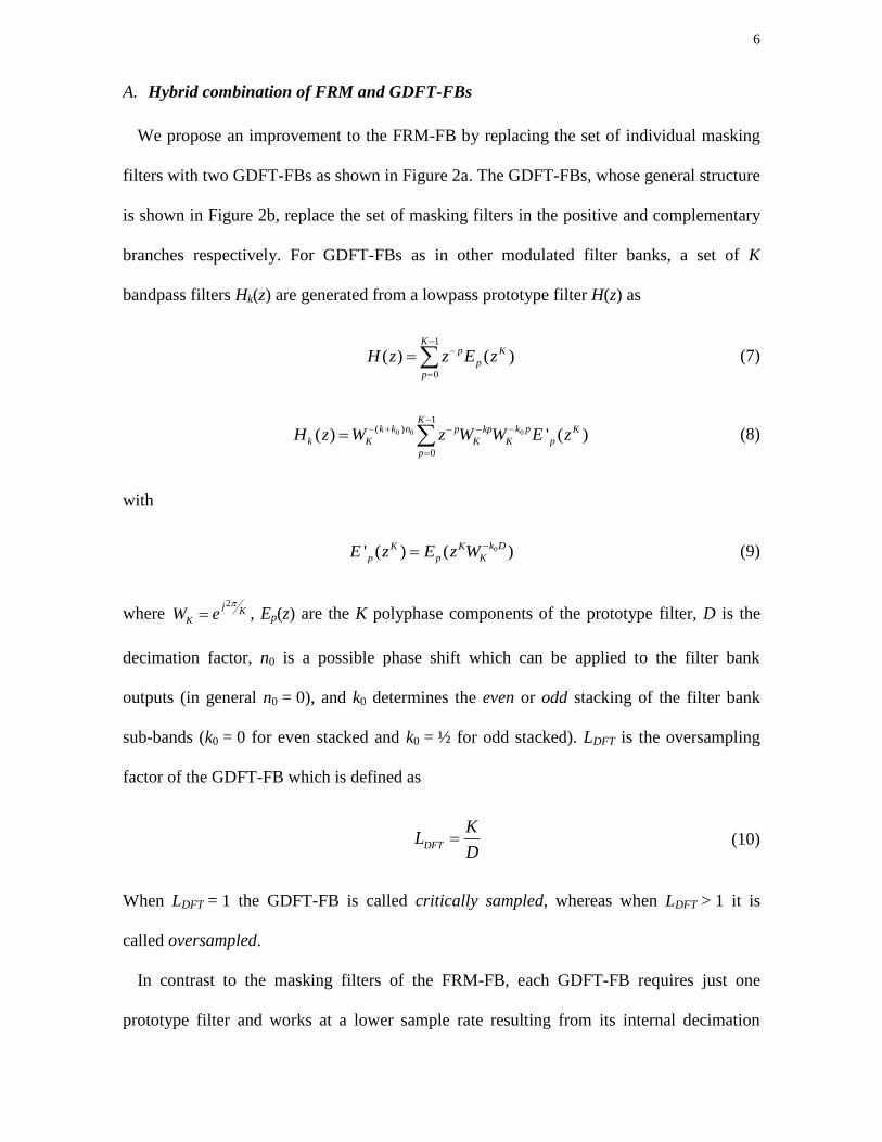
A. Hybrid combination of FRM and GDFT-FBs
We propose an improvement to the FRM-FB by replacing the set of individual masking
filters with two GDFT-FBs as shown in Figure 2a. The GDFT-FBs, whose general structure
is shown in Figure 2b, replace the set of masking filters in the positive and complementary
branches respectively. For GDFT-FBs as in other modulated filter banks, a set of K
bandpass filters Hk(z) are generated from a lowpass prototype filter H(z) as
1
0
( ) ( )K
p K
p
p
H z z E z
(7)
0 0 0
1( )
0
( ) ' ( )K
k k n k pp kp K
k K K K p
p
H z W z W W E z
(8)
with
0' ( ) ( )k DK K
p p KE z E z W
(9)
where 2j
KKW e
, Ep(z) are the K polyphase components of the prototype filter, D is the
decimation factor, n0 is a possible phase shift which can be applied to the filter bank
outputs (in general n0 = 0), and k0 determines the even or odd stacking of the filter bank
sub-bands (k0 = 0 for even stacked and k0 = ½ for odd stacked). LDFT is the oversampling
factor of the GDFT-FB which is defined as
DFT
KL
D (10)
When LDFT = 1 the GDFT-FB is called critically sampled, whereas when LDFT > 1 it is
called oversampled.
In contrast to the masking filters of the FRM-FB, each GDFT-FB requires just one
prototype filter and works at a lower sample rate resulting from its internal decimation

7
operations. This hybrid of the FRM-FB and GDFT-FB is called the Hybrid GDFT-FB
(H-GDFT). In the H-GDFT, as in the FRM-FB, the interpolated versions of the base filter
and complementary filter each extract half of the wideband input signal channels: the even
and odd channels respectively.
To ensure that base and complementary filter images have the same passband and
transition band widths, the base filter is designed as a half-band filter with its transition
band centred at π/2 rad, as shown in Figure 3a.
The interpolation factor of the base half-band filter, L, is determined by the number of
sub-bands of the GDFT-FBs according to
2
KL (11)
where K is the number of sub-bands in the GDFT-FBs. Therefore, considering the desired
final frequency response passband (ωp) and stopband (ωs) cut-off frequencies, the FRM
base filter passband (θ) and stopband (φ) specifications are given by
pL (12)
sL (13)
The initial filtering performed by the base and complementary filters yields two
multi-channel signals, wa(n) and wc(n) in Figure2 and Figure 3, each of which contains a
null for every second channel. This benefits the prototype filter design of the masking
GDFT filter banks in two ways. First, each GDFT-FB can be critically sampled because of
reduced aliasing from adjacent bands. Second, the transition band constraints of the
GDFT-FB prototype filters can be relaxed (relative to a design without the base and
complementary pre-filters) thereby reducing its order. Specifically, the GDFT-FB prototype

8
filters can be designed with a less sharp transition band between π/K and 2π/K rad.
Figure 3b-e show the two-stage filtering operation for the positive and complementary
branch of the H-GDFT. For both of them, the first stage is the same as in the FRM-FB, with
the images of the interpolated base (Figure 3b) and complementary (Figure 3d) filters
selecting the set of even and odd channels respectively. In the second stage, the bandpass
filters formed by each of the GDFT-FBs cascaded with the base (Figure 3c) and
complementary (Figure 3e) filters extract the individual channels from wa(n) and wc(n)
respectively.
To ensure that both the base and complementary filter images are centred exactly at the
same centre frequencies as the GDFT-FBs sub-bands, the input sample rate of the
multi-channel signal needs to satisfy
S CSf K f (14)
where fCS represents the desired sub-band channel spacing.
Since half of the sub-bands are null (unused) in each GDFT-FB, further reductions in
channelizer computation can be achieved. If only every I-th sub-band of a GDFT-FB is
employed to receive information, a K-point DFT or FFT operation can be replaced by a
(K/I)-point DFT or FFT [1].
The only condition that has to be met is that K is an integer multiple of I as
K Q I (15)
Since only Q of the output sub-bands are needed, then only Q of the DFT input samples
have to be computed. Figure 4 shows a GDFT-FB design where each sq(n) signal is created
as a time aliased version of a number I of rk(n) signals [1]. The time aliased signal is
obtained according to

9
1
0
( ) ( ) 0 1I
q q Qi
i
s n r n q Q
(16)
As a result only the sub-bands containing actual information channels are processed by the
DFT (or FFT).
In the particular case of the H-GDFT, I = 2 since only every second sub-band is
effectively used. Therefore, the K-point DFT operations in each GDFT-FB in Figure 2a can
be replaced by a K/2-point (or Q-point) DFT. Consequently, the computation of the null
sub-bands is saved leading to the more efficient implementation.
B. Filter design example
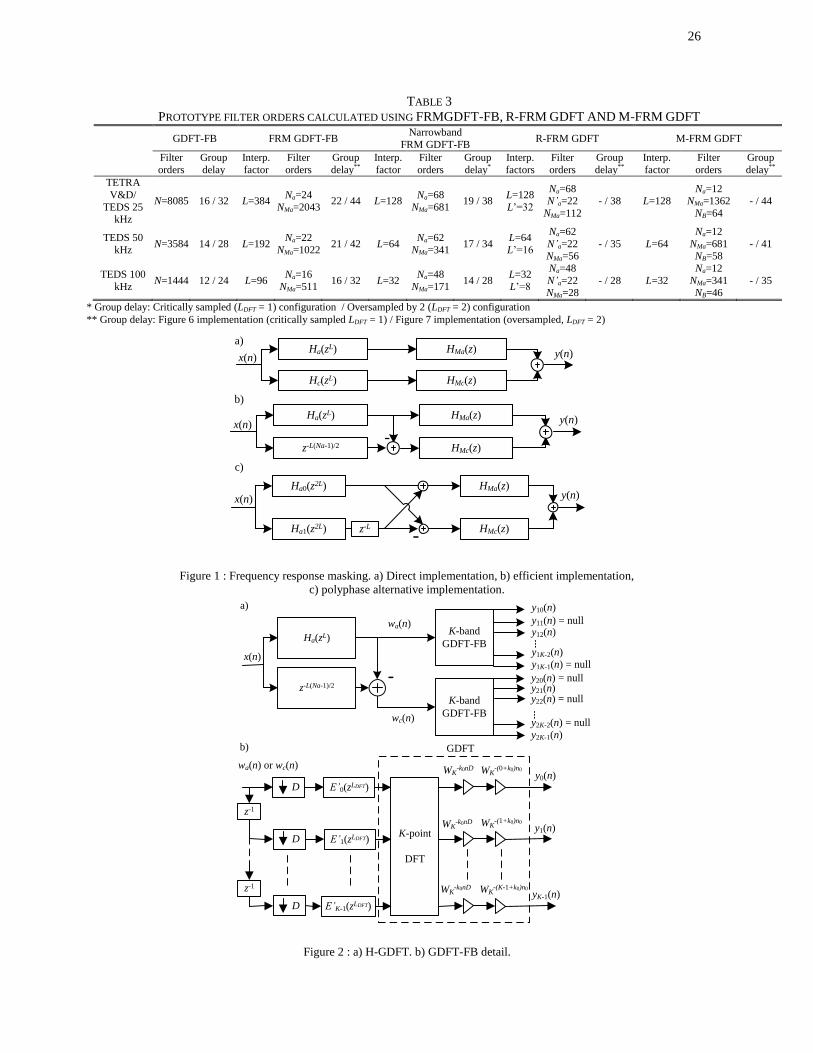
Using the GDFT-FB designs for TETRA V&D and TEDS channels from [3], the
theoretical prototype filter orders required for GDFT-FB and H-GDFT designs are
compared in Table 2. As in [3], the prototype filters were designed as FIR optimum
equiripple filters with orders estimated using Kaiser’s equation for equiripple filters [22].
Although the H-GDFT designs are composed of two filtering stages instead of one in the
GDFT-FB, the base (Na) and prototype filters (N) have a much larger transition band
thereby reducing the number of coefficients by between 76.7% and 83.2%.
In addition, Table 2 shows the group delay expressed in number of output samples for
both channelizer designs. This group delay is affected by the filter bank decimation factor,
and consequently varies for critically sampled and oversampled configurations, as shown in
the table. When translated into a time delay by multiplying the number of output samples
by the output sample period, both of them become equal since the output sample period of
the oversampled channelizer is half of the period of the critically sampled channelizer.
Although the H-GDFT requires a smaller number of coefficients, the large interpolation
factors applied to the base filter in this design example leads to larger group delays than the

10
GDFT-FB, and consequently longer transient responses. Generally the length of the
transient response of an FIR filter is not relevant in the field of communications, however,
the time delay associated with it will contribute to the overall latency in the signal path, and
therefore should be considered for real-time or delay-sensitive services.
To examine frequency response differences between the GDFT-FB and H-GDFT
channelizers both methods where used to design an oversampled (LDFT = 2) channelizer for
eight TETRA V&D 25 kHz channels. The theoretical filter orders for the optimum
equiripple designs were N = 253 for the GDFT-FB and Na=64 and N=42 for the H-GDFT.
Note that this is not a constraint and any desired digital filter design process could be used
for the prototype filter, e.g. window method [20]. Due to aliasing effects [23], the filter
orders had to be increased to N=280 for GDFT-FB and Na=70 and N=52 for the H-GDFT in
order to meet the filtering specifications in [3].
Figure 5a shows the magnitude response of the two designs, whereas Figure 5b focuses
on the passband ripple. In the stopband, the H-GDFT response decreases with increasing
frequency and this reduces the adjacent channel interference in comparison with the almost
constant ripple of the GDFT-FB design. In the passband the magnitude response of the two
channelizers also differs despite equiripple filter designs being used for all filters. The
H-GDFT passband response exhibits non-uniform ripple caused by the cascading of several
filters in its implementation. Nevertheless the passband ripple and stopband attenuation
specifications are still met.
III. FRM GDFT-FB
An alternative approach to integrating FRM with the GDFT-FB is to directly apply FRM
to the prototype filter implementation. Previous researchers have applied the FRM
technique to the prototype filter design of cosine modulated filter banks for cases where

11
real signals are processed [15-17]. However, FRM has not been applied in this way to
complex valued signals and in particular it has not been applied to complex modulated filter
banks. Therefore we next extend the approach taken in the combined FRM and cosine
modulated filter bank design [17] to complex signals and the GDFT-FB.
Substituting (4) and (5) into (1), the prototype filter H(z) can be expressed as
2 2 2 2
0 1 1 1( ) ( ) ( ) ( ) ( ) ( ) ( ) ( ) ( )L L L L L L
a Ma a Ma a Mc a McH z H z H z z H z H z H z H z z H z H z (17)
Identifying the common components in (17), this can be rearranged as
( ) ( ) ( )
( ) ( ) ( )
Ma Mc
Ma Mc
A z H z H z
B z H z H z
(18)
2 2
0 1( ) ( ) ( ) ( ) ( )L L L
a aH z H z A z z H z B z (19)
In addition, the polyphase decomposition can be applied to the masking filters to yield
1
0
1
0
( ) ( )
( ) ( )
Ki K
Ai
i
Ki K
Bi
i
A z z E z
B z z E z
(20)
where EAi(z) and EBi(z) are the K polyphase components of A(z) and B(z) respectively.
The GDFT-FB modulated bandpass filters may be created from the lowpass prototype by
application of the complex modulation in (9)
0
0
2 2
0 1( ) ( ) ( ) ( ) ( )
( ) ( )
( ) ( )
L L L
k a k a k
k k
k K
k k
k K
H z H z A z z H z B z
A z A zW
B z B zW
(21)
Finally, each of the modulated bandpass filters is given by
0 0
1 12 2
0 1
0 0
( ) ( ) ' ( ) ( 1) ( ) ' ( )K K
k i k iL i ki K k L L i ki K
k a K K Ai a K K Bi
i i
H z H z z W W E z z H z z W W E z
(22)

12
where
0
0
' ( ) ( )
' ( ) ( )
k DK K
Ai Ai K
k DK K
Bi Bi K
E z E z W
E z E z W
(23)
The resulting FRM GDFT-FB structure is shown in Figure 6. For the outputs with odd
indexes (k =1,3,…, K-1) there is a phase difference of π rad between the two polyphase
components E’Ai(zK) and E’Bi(z
K) in (22) as in [17]. Therefore, a phase rotation must be
applied to the wk(n) signals with odd indexes as shown in Figure 6. For the odd stacked
configuration, it is necessary to make k0 = ½ and, at design time, to shift the frequency
response of the base filter to be centred at π/2 rad.
Given the desired passband and stopband cut-off specifications for the prototype filter
(ωp and ωs), the base and masking filters are designed using the expressions in Table 1. In
addition, the value of the FRM interpolation factor is chosen according to
Case 1: (4 1)2
Case 2: (4 1)2
KL m
KL m
(24)
where m is any integer equal to or greater than 1.
A. Narrowband FRM GDFT-FB
The FRM GDFT-FB structure in Figure 6 can be adapted for cases where a narrowband
prototype filter is appropriate by only employing the FRM positive branch. For this case,
(18) simplifies to
( ) ( ) ( )MaA z B z H z (25)
Therefore, the prototype filter and the polyphase decomposition of the positive masking
filter are given by

13
2 2
0 1( ) ( ) ( ) ( ) ( )L L L
a Ma a MaH z H z H z z H z H z (26)
1
0
( ) ( )K
i K
Ma Mai
i
H z z E z
(27)
Consequently, for the narrowband FRM GDFT-FB the modulated bandpass filters in (22)
become
0 0
1 12 2
0 1
0 0
( ) ( ) ' ( ) ( 1) ( ) ' ( )K K
k i k iL i ki K k L L i ki K
k a K K Mai a K K Mai
i i
H z H z z W W E z z H z z W W E z
(28)
where
0' ( ) ( )k DK K
Mai Mai KE z E z W
(29)
For the narrowband FRM GDFT-FB, as for the H-GDFT, there is just one possible value
for the interpolation factor L given by (11). Using L, the specifications for the base filter
and the positive masking filter may be calculated using Table 1. Comparing (28) with (22),
it should be clear that the filter bank must be implemented using the same basic structure
(shown in Figure 6) in both the full FRM and narrowband FRM cases.
B. Alternative oversampled FRM GDFT-FB
In the FRM GDFT-FB structure of Figure 6 the base filter is placed before the modulated
GDFT-FB structure. Consequently, it must operate at a much higher rate than the masking
filter. In addition, when the number of channels, K, is large the base filter interpolation
factor, which must comply with (24), requires large zero padding and delay in the base
filter polyphase components.
Based on the approach taken in [17], an alternative FRM GDFT-FB structure can be
realized. In the alternative structure shown in Figure 7a, the base filter is commuted to the
lower sample rate output side of the filter bank using the noble identities. In addition to

14
performing base filter operations at the lowest sample rate, the interpolation factor applied
to the base filter is reduced by a factor equal to the decimation, thereby reducing the zero
padding. The structure does, however, require an instance of the commuted base filter on
each GDFT-FB output, but this has the benefit that these filters will be real for both even
and odd-stacked configurations. This differs from the odd-stacked configuration of the
structure in Figure 6 which requires a complex base filter.
For the alternative FRM GDFT-FB to work, the filter bank must be oversampled
(LDFT > 1) and the oversampling factor LDFT must also be an even number. By applying (10)
in (24) and restricting LDFT to an even number bigger than one, it can be seen that the base
filter interpolation factor (2L/D) and the complementary delays (L/D) in Figure 7a are
integers. This structure is not suitable for critically sampled (LDFT = 1) filter banks or filter
banks with an odd oversampling factor because the base filter interpolation factor would
not be an integer.
In the narrowband FRM case, the structure in Figure 7a can be simplified, leading to the
more efficient structure shown in Figure 7b. In this variant, the polyphase decomposition of
the base filter is avoided, so an interpolated version of the base filter can be used directly.
In addition, since the base filter is not divided into polyphase components, symmetry in its
coefficients can be exploited to reduce the number of multiplications required.
C. Recursive and multi-stage FRM GDFT-FB
Further reductions in the number of coefficients per filter can be achieved by applying
recursive and multi-stage techniques to any of the FRM GDFT-FBs already introduced in
this work. The recursive structure consists of a second FRM structure applied to the base
filter itself. The increased complexity of the design makes it tedious to implement for the
full FRM GDFT-FB but it has been applied to the narrowband FRM GDFT-FB [15].

15
The recursive narrowband FRM structure is realized by the addition of a second base
filter, H’a(zL’
), cascaded with the base filter, Ha(zL), and complementary filters, HMa(z), as
shown in Figure 8a. The second base filter assists the masking filter by eliminating some of
the unwanted images arising from interpolation of the first base filter as depicted in Figure
8b. To achieve this, the second base filter’s interpolation factor, L’, needs to be smaller than
L. Following the two base filters, a masking filter with a wider transition band (and lower
order) than in the normal FRM implementation is used to remove the remaining images of
the base filter.
The passband and stopband cut-off frequencies of the (first) base filter are the same as for
the normal narrowband FRM implementation given by Table 1. For the recursive (second)
base filter H’a(z) and the masking filter the design specifications are given by
2' ' ' '
2 2
'
p s
Mpa p Msa s
L LL
L L
(30)
This structure can be integrated into both the basic (Figure 6) and alternative narrowband
(Figure 7b) FRM GDFT-FBs already described by adding the second base filter at the input
of the filter bank. This new configuration is referred to as the Recursive FRM GDFT-FB
(R-FRM GDFT).
As an alternative to recursive FRM, multi-stage filtering techniques can be used to reduce
the order of the prototype filter in an FRM GDFT-FB. As in [3], the prototype filter
specification is relaxed by increasing its transition band to include parts of the adjacent
channels. Thereafter, a second stage comprising half-band filters, HB(z), at the filter bank
output eliminates the extra undesired signal, leaving just the desired frequency band. As in
[3], it is necessary that the uniform filter bank uses an oversampled configuration

16
(specifically LDFT = 2) in order to be able to use half-band filters at the outputs. Since this
multi-stage structure requires oversampling whether using the basic or the alternative
narrowband FRM GDFT-FB (Figure 6 and Figure 7b respectively), the multi-stage variant
of the alternative narrowband FRM GDFT-FB (M-FRM GDFT) represents the most
efficient design in which to apply it.
In FRM designs, passband and stopband ripples from the base filter and masking filter
frequency responses both contribute to the final composite frequency response. Because of
this the passband and stopband specifications for the base and masking filters must be more
stringent than the final filter. According to [20], a useful guideline is to make the base filter
passband and stopband ripple and the masking filter passband ripple specifications 20%
more stringent than the composite frequency response requires; a masking filter stopband
ripple that is 50% more stringent is also recommended.
The R-FRM GDFT and M-FRM GDFT designs are compared by applying them to an
eight channel TETRA V&D channelizer, similar to the H-GDFT design example in Figure
5. Since an oversampled configuration (LDFT = 2) is required for the M-FRM GDFT, both
the R-FRM GDFT and M-FRM GDFT are designed as oversampled to compare their
output frequency responses. For both cases the theoretical filter orders are calculated
considering the overdesign considerations. For the R-FRM GDFT the filter orders obtained
are Na = 68, N'a = 22 and NMa = 112. In this case, the passband and stopband specifications
are met at the channelizer outputs. For the corresponding M-FRM GDFT the calculated
filter orders are Na = 12, NMa = 1362 and NB = 64, where NB is the order of the half-band
filters. However, for the M-FRM GDFT, with these filter orders the desired output
specifications are still not achieved (similar to the H-GDFT) and, therefore, an increase in
the half-band filter order to NB=70 is necessary.
Both frequency responses are shown in Figure 9. Both designs have similar frequency

17
response in the passband and transition band, but the M-FRM GDFT provides more
attenuation in the stopband due to the half-band filter after the filter bank outputs. For both
cases the passband peak-to-peak ripple is within the limits. Similar to the H-GDFT in
Figure 5, the filter passband magnitude response is not equiripple due to the contribution of
several filters to the final frequency response.
D. FRM GDFT-FB design examples and computational comparison
The comparison of the different proposed FRM GDFT-FB designs is based on four
factors: filter frequency response, filter orders, group delay, and computational load. In
terms of frequency response, the filter bank specifications given in Table 2 for the TETRA
V&D and TEDS uniform filter banks are adapted for the FRM GDFT-FB, R-FRM GDFT
and M-FRM GDFT channelizers according to the more stringent requirements for FRM
designs [20].
Secondly, the filter orders and group delay of each design are compared in Table 3. In it,
the order of all filter theoretical orders are calculated following the overdesign
considerations expressed in [22]. Group delay calculations masured in number of output
samples are also tabulated.
For the full FRM GDFT-FB design, only the calculation of the base (Na) and masking
filters (NMa, NMc) orders is required since both masking filters have the same order, NMa. To
calculate the filter orders, first, a particular positive integer value is given to the variable m.
This value is used in (24) to obtain the FRM interpolation factor L for either the design case
1 or case 2. Finally, for the chosen design case and the values of m and L, the base and
masking filter specifications are given by the expressions in Table 1. In general, according
to [24], it has been demonstrated that the variations in the filter specifications and filter
orders produced by an increase in the value of m (which implies an increase in L) produces

18
an increase in the computational load of the FRM GDFT-FB channelizer. In addition, for a
given value of m, design case 2 leads to smaller computational load than case 1. Therefore,
in Table 3 m = 1 and case 2 designs are used for the three types of channel.
For the narrowband FRM GDFT-FB there is one single possible value of the
interpolation value, L, given by (11). In this design just one base filter, Ha(z), and one
masking filter, HMa(z), are required. Comparing the filter orders for both full
FRM GDFT-FB and narrowband FRM GDFT-FB, it can be observed that in general the
base filter order (Na) is larger in the second design. This is a direct consequence of the
smaller interpolation factor L employed in the narrowband case, which leads to a base filter
specification with a smaller transition band. On the other hand, the masking filter order
(NMa) is generally smaller in the narrowband design since its transition band specification is
more relaxed in this case.
The R-FRM GDFT is characterized by the use of one base filter, Ha(z), one recursive
base filter, H'a(z), and one masking filter, HMa(z). Each of the base filters has its own
interpolation factor, L and L’ respectively. In this design, the base filter order (Na) and
interpolation factor remain the same as in the narrowband FRM GDFT-FB case since the
function of the recursive filter is just to aid the masking filter.
Finally, the M-FRM GDFT does not incorporate a recursive base filter but instead
includes a half-band filter, HB(z), on every output sub-band of the filter bank. The half-band
filters allow relaxation of the base filter specifications leading to smaller orders than the
narrowband FRM GDFT-FB design. However, the more relaxed interpolated version of the
base filter adversely affects the filtering requirements for the masking filter and increases
its order in comparison with the narrowband FRM GDFT-FB case.
Table 3 shows that all the FRM methods benefit from significantly shorter individual
filters and fewer coefficients in total than the classic GDFT-FB. The smallest saving was

19
achieved by the full FRM GDFT-FB with up to 50% fewer coefficients, while the R-FRM
GDFT provided the largest saving with up to 95% fewer coefficients.
Examining group delay, Table 3 shows that all FRM GDFT-FB channelizers suffer larger
group delays than the classic GDFT-FB design for both critically sampled and oversampled
configurations. Again, it can be observed how the group delay is proportional to the
oversampling factor (LDFT) used in the channelizer. Among the different designs, the
narrowband FRM GDFT-FB and R-FRM GDFT provided the smallest group delays.
Despite the significantly reduced filter orders required by the filter bank designs
employing the FRM technique, a reduction in their computational load with respect to the
classic GDFT-FB cannot be guaranteed. Therefore, a computational analysis comparison of
the FRM filter bank designs with the classic GDFT-FB for different use case scenarios is
necessary. For this evaluation the TETRA V&D, TEDS 50 kHz and TEDS 100 kHz
standards were used. For each filter bank, an odd-stacked uniform channelizer was
designed using the filter bank specifications of Table 2 and the filter orders calculated in
Table 3. The comparison baseline is the number of real multiplications required per
complex input sample. The input of the channelizer is considered to be a wideband
complex baseband signal containing all channels. The computational loads for each
channelizer are extracted from [8]. In general, the size of the DFT in the GDFT-FB is
chosen equal to a power-of-two to permit use of the radix-2 Fast Fourier Transform (FFT).
The radix-2 FFT algorithm is considered since it is very commonly implemented in DSP
devices such as FPGAs [25]. Nevertheless, all the FRM GDFT-FB designs are independent
of the FFT algorithm employed and more efficient algorithms may be employed, such as
the Good-Thomas or prime factor algorithm [25], which reduce the computation and do not
require a power-of-two DFT size.
Figure 10 presents the computational load differences between the various uniform

20
channelizer designs. In particular, Figure 10a shows the channelizer options for the
critically sampled case. For the FRM methods only the design in Figure 6 is applicable in
this situation (for both full and narrowband FRM). Among the critically sampled
channelizers, it is apparent that the narrowband FRM GDFT-DB requires most operations
per input sample while the full FRM GDFT-FB requires just slightly more than the classic
GDFT-FB. The reason for this is the higher order base filter in the narrowband case relative
to the full FRM case. This is despite the narrowband FRM GDFT-FB having fewer overall
coefficients than the full FRM equivalent (as seen in Table 3). For the structure in Figure 6
the base filter performs at the highest sample rate in comparison with the rest of the filters
forming the filter bank. Therefore, small increments in the base filter order represent
considerable increments in the computational load.
Finally, Figure 10b shows that when oversampled channelizer configurations are used all
the combined FRM and GDFT-FB designs require fewer operations per input sample than
the GDFT-FB. In particular, the efficient oversampled narrowband FRM GDFT-FB
structure (Figure 7b) requires approximately half the multiplications of the other designs.
Moreover, unlike the other oversampled designs, the oversampled narrowband FRM
GDFT-FB requires fewer multiplications than any of the critically sampled designs.
IV. COMBINED FRM AND GDFT-FB DESIGNS APPLIED TO NON-UNIFORM
CHANNELIZATION AND DSA
To evaluate non-uniform channelization based on the combined FRM and GDFT-FB
designs compared to the GDFT-FB, we consider a DSA use case comprising a mix of
TETRA V&D and TEDS channels covering a 5 MHz frequency band as in [8]. The
(baseband) multi-channel DSA configuration is always odd-stacked (no channel centred at
DC). Three different channel allocation configurations are considered:

21
Configuration 1: 100 x 25 kHz TETRA V&D channels, 26 x TEDS 50 kHz channels,
and 12 x TEDS 100 kHz channels.
Configuration 2: 52 x 25 kHz TETRA V&D channels, 50 x TEDS 50 kHz channels, and
12 x TEDS 100 kHz channels.
Configuration 3: 50 x 25 kHz TETRA V&D channels, 25 x TEDS 50 kHz channels, and
25 x TEDS 100 kHz channels.
Non-uniform channelizers based on the combined FRM and GDFT-FB designs were
realized using the same parallel and recombined structures applied to the GDFT-FB (see
Figure 11a and Figure 11b) but substituting the appropriate uniform filter bank for the
GDFT-FB. The design parameters in Table 1 and filter orders in Table 2 and Table 3 were
used for the 25 kHz, 50 kHz and 100 kHz uniform filter banks. The alternative form
oversampled narrowband FRM GDFT-FB proved to be the most efficient FRM based
uniform design and this design was therefore used as the basis for all FRM configurations
evaluated, including the R-FRM GDFT, and M-FRM GDFT.
Figure 11c and Figure 11d shows the results for parallel and recombined filter bank
channelizer implementations based on the GDFT-FB and combined FRM and GDFT filter
banks for all three channel allocation configurations in the evaluation use case. It is clear
that the M-FRM GDFT filter bank is the basis for the most computationally efficient non-
uniform channelizers using either the parallel or the recombined filter bank structure.
Furthermore, the recombined filter bank structures were all more efficient than their
parallel counterparts for the configurations evaluated. In particular, the most efficient
recombined M-FRM GDFT channelizer needed up to 60% fewer operations than the
corresponding parallel channelizer. In general, all the combined FRM and GDFT designs
led to lower computational loads than the Parallel GDFT and Recombined GDFT

22
implementations using the classic GDFT-FB.
The Parallel R-FRM GDFT is the only exception where no computational reduction is
achieved with respect to the classic GDFT-FB implementation. However, this particular
filter bank provides the lowest filter orders among all designs, as can be seen in the
coefficient calculation in Table 3. Depending on the application, low filter orders can be as
important as low computational load. For example, in fixed-point implementations the
lower the filter order the less sensitive the frequency response of the filter will be to
coefficient quantization errors [26].
In conclusion, the Recombined R-FRM GDFT provides the best overall performance
considering both the number of coefficients and computational load. Even though some
other designs require fewer operations, the R-FRM GDFT benefits from low filter orders
for all the filters composing the channelizer, unlike the other designs which yield a mixture
of low order and high order filters. In addition, the R-FRM GDFT employs half-band
filters (like all the other FRM GDFT-FB designs) which achieve the required magnitude
complementary property required for sub-band recombination automatically.
V. CONCLUSION
In this paper a novel combination of the FRM structure and GDFT-FBs was presented for
efficient uniform and non-uniform channelization methods. In particular, two principal
approaches were evaluated: cascading the FRM structure with a GDFT-FB and using FRM
more directly to implement the GDFT-FB prototype filter more efficiently. Both
approaches were analysed for different channel stacking configurations, oversampling
factors, and type of FRM (full or narrowband). All of the combined FRM and GDFT-FB
structures showed a reduction in the number of coefficients (up to 95%) compared to the
basic GDFT-FB implementation. In addition, considering their computational load, all

23
uniform and non-uniform channelizer designs (with the exception of the uniform FRM
GDFT-FB and non-uniform parallel R-FRM GDFT) yielded reductions relative to the basic
GDFT-FB based channelizers. However, they all showed larger group delays. Overall, all
the combined FRM and GDFT-FB structures presented in this paper outperformed
GDFT-FBs in at least one of the comparison parameters, hence leaving the final decision of
choosing which structure suits better the purpose of the design to the engineer.
VITAE
Álvaro Palomo-Navarro received his B.Eng. degree in telecommunications engineering from the
Polytechnic University of Madrid, Spain, in 2006, and his Ph.D. degree from the National University of
Ireland, Maynooth, Ireland, in 2011. Between 2006 and 2007 he worked as a test engineer for GSM
intelligent networks. Since 2007 he has worked in the Electronic Engineering Department at the National
University of Ireland, Maynooth. His main research interests include multirate DSP, SDR, DSA and
multi-standard wireless communications.
Ronan J. Farrell received his B.E. and Ph.D. degrees in electronic engineering from University College
Dublin, Ireland, in 1993 and 1998. He is currently a senior lecturer at the National University of Ireland,
Maynooth, and director of the Callan Institute for applied ICT. His research interests include physical layer
communication technologies, in particular, adaptive receivers, PAs, and active antenna arrays. He is currently
the strand leader responsible for radio technologies in the SFI-funded Centre for Telecommunications
Research.
Rudi Villing received his B.Eng. degree in electronic engineering from Dublin City University, Ireland, in
1992, and his Ph.D. degree from the National University of Ireland, Maynooth, Ireland, in 2010. He is
currently a lecturer at the National University of Ireland, Maynooth, having previously worked in the
telecommunications software industry. His research interests include communications and wireless systems
(particularly at the interface between the physical infrastructure and the software defined environment) and
perceptual signal processing.
REFERENCES
[1] K. C. Zangi and R. D. Koilpillai, "Software radio issues in cellular base stations," Selected Areas in

24
Communications, IEEE Journal on, vol. 17, pp. 561-573, 1999.
[2] T. Hentschel, "Channelization for software defined base stations," Annales de Telecommunications,
May/June 2002.
[3] A. Palomo Navarro, R. Villing, and R. Farrell, "Practical Non-Uniform Channelization for Multi-
standard Base Stations," ZTE Comms. Journal. Special topic: Digital Front-End and Software Radio
Frequency in Wireless Communication and Broadcasting, vol. 9, December 2011.
[4] E. Hossain, D. Niyato, and D. I. Kim, "Evolution and future trends of research in cognitive radio: a
contemporary survey," Wireless Communications and Mobile Computing, pp. n/a-n/a, 2013.
[5] F. Khozeimeh and S. Haykin, "Dynamic spectrum management for cognitive radio: an overview,"
Wireless Communications and Mobile Computing, vol. 9, pp. 1447-1459, 2009.
[6] P. Leaves, K. Moessner, R. Tafazolli, D. Grandblaise, D. Bourse, R. Tonjes, and M. Breveglieri,
"Dynamic spectrum allocation in composite reconfigurable wireless networks," Communications
Magazine, IEEE, vol. 42, pp. 72-81, 2004.
[7] A. Boukerche, K. El-Khatib, and T. Huang, "A performance evaluation of distributed dynamic
channel allocation protocols for mobile networks," Wireless Communications and Mobile
Computing, vol. 7, pp. 69-80, 2007.
[8] A. Palomo Navarro, T. Keenan, R. Villing, and R. Farrell, "Non-uniform channelization methods for
next generation SDR PMR base stations," in Computers and Communications (ISCC), 2011 IEEE
Symposium on, 2011, pp. 620-625.
[9] W. A. Abu-Al-Saud and G. L. Stuber, "Efficient wideband channelizer for software radio systems
using modulated PR filterbanks," Signal Processing, IEEE Transactions on, vol. 52, pp. 2807-2820,
2004.
[10] F. J. M. G. Harris, R., "A receiver structure that performs simultaneous spectral analysis and time
series channelization," in Proceedings of the SDR'09 Technical Conference and Product Exposition,
2009.
[11] A. Eghbali, H. Johansson, and P. Lowenborg, "Reconfigurable Nonuniform Transmultiplexers Using
Uniform Modulated Filter Banks," Circuits and Systems I: Regular Papers, IEEE Transactions on,
vol. PP, pp. 1-1, 2010.
[12] A. Eghbali, H. Johansson, and P. Lowenborg, "A Farrow-structure-based multi-mode
transmultiplexer," in Circuits and Systems, 2008. ISCAS 2008. IEEE International Symposium on,
2008, pp. 3114-3117.
[13] R. Mahesh, A. P. Vinod, E. M. K. Lai, and A. Omondi, "Filter Bank Channelizers for Multi-Standard
Software Defined Radio Receivers," Journal of Signal Processing Systems, Springer New York,
2008.
[14] R. Mahesh and A. P. Vinod, "Reconfigurable Frequency Response Masking Filters for Software
Radio Channelization," Circuits and Systems II: Express Briefs, IEEE Transactions on, vol. 55, pp.
274-278, 2008.
[15] L. C. R. de Barcellos, "Estruturas Eficientes de Transmultiplexadores e de Bancos de Filtros
Modulados por Cossenos," PhD, Electronic Engineering, COPPE/UFRJ, Rio de Janeiro, 2006.
[16] S. L. Netto, P. S. R. Diniz, and L. C. R. Barcellos, "Efficient implementation for cosine-modulated
filter banks using the frequency response masking approach," in Circuits and Systems, 2002. ISCAS
2002. IEEE International Symposium on, 2002, pp. III-229-III-232 vol.3.
[17] L. Rosenbaum, P. Lowenborg, and H. Johansson, "An approach for synthesis of modulated M-
channel FIR filter banks utilizing the frequency-response masking technique," EURASIP J. Appl.
Signal Process., vol. 2007, pp. 144-144, 2007.
[18] M. B. Furtado, Jr., P. S. R. Diniz, S. L. Netto, and T. Saramaki, "On the design of high-complexity
cosine-modulated transmultiplexers based on the frequency-response masking approach," Circuits
and Systems I: Regular Papers, IEEE Transactions on, vol. 52, pp. 2413-2426, 2005.
[19] L. Yong, "Frequency-response masking approach for the synthesis of sharp linear phase digital
filters," Circuits and Systems, IEEE Transactions on, vol. 33, pp. 357-364, 1986.
[20] P. S. R. Diniz, E. A. B. da Silva, and S. L. Netto, Digital Signal Processing: System Analysis and

25
Design: Cambridge University Press, 2002.
[21] H. Johansson, "New classes of frequency-response masking FIR filters," in Circuits and Systems,
2000. Proceedings. ISCAS 2000 Geneva. The 2000 IEEE International Symposium on, 2000, pp. 81-
84 vol.3.
[22] J. Kaiser, "Nonrecursive Digital Filter Design Using the IO-Sinh Window Function," in IEEE
International Symposium on Circuits and Systems, 1974.
[23] Q.-G. Liu, B. Champagne, and D. K. C. Ho, "Simple design of oversampled uniform DFT filter
banks with applications to subband acoustic echo cancellation," Signal Processing, vol. 80, pp. 831-
847, 2000.
[24] A. Palomo Navarro, "Channelization for Multi-Standard Software-Defined Radio Base Stations,"
PhD, Electronic Engineering Dept., National University of Ireland, Maynooth, 2011.
[25] P. Duhamel and M. Vetterli, "Fast fourier transforms: a tutorial review and a state of the art," vol.
19, ed: Elsevier North-Holland, Inc., 1990, pp. 259-299.
[26] J. G. Proakis and D. G. Manolakis, Digital signal processing: Principles, Algorithms and
Applications: Pearson Prentice Hall, 2007.
TABLE 1
FRM FILTERS SPECIFICATIONS CALCULATION
Full FRM
(Case 1)
Full FRM
(Case 2)
Narrowband FRM
Base filter 2
2
p
s
L m
L m
2
2
s
p
m L
m L
p
s
L
L
Positive Masking filter
HMa(z)
2
2( 1)
Mpa
Msa
m
L
m
L
2( 1)
2
Mpa
Msa
m
L
m
L
2
Mpa p
Msa sL
Complementary
Masking filter
HMc(z)
2
2
Mpc
Msc
m
L
m
L
2
2
Mpc
Msc
m
L
m
L
n/a
TABLE 2
PROTOTYPE FILTER ORDERS CALCULATED USING H-GDFTS FOR THE SPECIFICATIONS IN [3].
Number
channels
(K)
GDFT-FB H-GDFT
Filter
order Group delay
*
Filter
order Group delay
*
TETRA V&D
/TEDS 25 kHz 256 N = 8085 16 / 32
Na = 64
N = 1294 19 / 38
TEDS 50 kHz 128 N = 3584 14 / 28 Na = 58
N = 595 17 / 34
TEDS 100 kHz 64 N = 1444 12 / 24 Na=46
N = 291 14 / 28
* Group delay: Critically sampled (LDFT = 1) configuration / Oversampled by 2 (LDFT = 2) configuration
26
Figure 1 : Frequency response masking. a) Direct implementation, b) efficient implementation,
c) polyphase alternative implementation.
Figure 2 : a) H-GDFT. b) GDFT-FB detail.
Ha(zL) HMa(z)
z-L(Na-1)/2 HMc(z)-
y(n)x(n)
b)
Ha(zL) HMa(z)
Hc(zL) HMc(z)
y(n)x(n)
a)
c)
Ha0(z2L) HMa(z)
Ha1(z2L) HMc(z)-
y(n)x(n)
z-L
Ha(zL)
z-L(Na-1)/2-
x(n)
y10(n)
y12(n)
y1K-2(n)
K-band
GDFT-FB
K-band
GDFT-FB
y11(n) = null
y1K-1(n) = null
a)
K-point
DFT
E’0(zLDFT)y0(n)
y1(n)
D
WK-k0nD WK
-(0+k0)n0
WK-k0nD WK
-(1+k0)n0
WK-k0nD WK
-(K-1+k0)n0
z-1
z-1
yK-1(n)
D
D
GDFTb)
E’1(zLDFT)
E’K-1(zLDFT)
wa(n)
wc(n)
y20(n) = null
y22(n) = null
y2K-2(n) = null
y21(n)
y2K-1(n)
wa(n) or wc(n)
TABLE 3
PROTOTYPE FILTER ORDERS CALCULATED USING FRMGDFT-FB, R-FRM GDFT AND M-FRM GDFT
GDFT-FB FRM GDFT-FB Narrowband
FRM GDFT-FB R-FRM GDFT M-FRM GDFT
Filter
orders
Group
delay
Interp.
factor
Filter
orders
Group
delay**
Interp.
factor
Filter
orders
Group
delay*
Interp.
factors
Filter
orders
Group
delay**
Interp.
factor
Filter
orders
Group
delay**
TETRA
V&D/
TEDS 25 kHz
N=8085 16 / 32 L=384 Na=24
NMa=2043 22 / 44 L=128
Na=68
NMa=681 19 / 38
L=128
L’=32
Na=68 N’a=22
NMa=112
- / 38 L=128 Na=12
NMa=1362
NB=64
- / 44
TEDS 50
kHz N=3584 14 / 28 L=192
Na=22
NMa=1022 21 / 42 L=64
Na=62
NMa=341 17 / 34
L=64
L’=16
Na=62
N’a=22 NMa=56
- / 35 L=64
Na=12
NMa=681 NB=58
- / 41
TEDS 100
kHz N=1444 12 / 24 L=96
Na=16
NMa=511 16 / 32 L=32
Na=48
NMa=171 14 / 28
L=32
L’=8
Na=48
N’a=22 NMa=28
- / 28 L=32
Na=12
NMa=341 NB=46
- / 35
* Group delay: Critically sampled (LDFT = 1) configuration / Oversampled by 2 (LDFT = 2) configuration
** Group delay: Figure 6 implementation (critically sampled LDFT = 1) / Figure 7 implementation (oversampled, LDFT = 2)

27
Figure 3 : H-GDFT filtering operations. a) Base filter and complementary filter magnitude responses. b) Even channels
filtered by interpolated base filter, c) then filtered by each of the bandpass filters forming the GDFT-FB. d) Odd channels
filtered by interpolated complementary filter, e) then filtered by each of the bandpass filters forming the GDFT-FB.
Figure 4 : GDFT-FB with DFT reduction.
πDC ω
|H10(ejω)|
-π π/K 2π/K-π/K-2π/K 3π/K 4π/K-4π/K -3π/K
πDC ω-π π/K 2π/K-π/K-2π/K 3π/K 4π/K-4π/K -3π/K
|H21(ejω)|
πDC ω
|Ha(ejωL)|
-π π/K 2π/K-π/K-2π/K 3π/K 4π/K-4π/K -3π/K
πDC ω-π π/K 2π/K-π/K-2π/K 3π/K 4π/K-4π/K -3π/K
|Hc(ejωL)|
b)
-(K-1)π/K (K-1)π/K
(K-1)π/K
(K-1)π/K
-(K-1)π/K
-(K-1)π/K
(K-1)π/K-(K-1)π/K
π-π/2 0
1
ω
|Ha(ejω)| |Hc(ejω)|
θ φ
a)
d)
|H12(ejω)||H1K-2(ejω)|
|H2K-1(ejω)| |H2(K/2+1)(ejω)|
c)
e)
π/2-π
Filters magnitude response Input signal X(ejω)
Wa(ejω) = Ha(ejωL)X(ejω) Wc(ejω) = Hc(ejωL)X(ejω)
K/2-point
GDFT
E’0(zL)
E’1(zL)
E’K-1(zL)
y0(n)
y1(n)
x(n) D
z-1
z-1
yQ-1(n)
TIME
ALIAS
BY
I
r0(n)
r1(n)
rK-1(n)
s0(n)
s1(n)
sQ-1(n)
D
D

28
Figure 5 : GDFT-FB and H-GDFT a) output sub-band channel magnitude response for an 8-channel TETRA V&D
channelizer, b) bandpass ripple detail.
Figure 6 : The GDFT-FB using full FRM.
0 0.1 0.2 0.3 0.4 0.5 0.6 0.7 0.8 0.9 1-100
-80
-60
-40
-20
0
20
Mag
nit
ude
resp
onse
(dB
)
0 0.05 0.1 0.15 0.2 0.25 0.3 0.35 0.4 0.45-0.08-0.06-0.04-0.02
00.020.040.060.08
Mag
nit
ude
resp
onse
(dB
)
GDFT-FBH- GDFT
Normalised frequency x π (rad)
Normalised frequency x π (rad)
a)
b)
E’A0(zLDFT)
E’A1(zLDFT)
E’A2(zLDFT)
GDFT
E’AK-1(zLDFT)
z-1
z-1
z-1
x(n)y0(n)
y1(n)
yK-1(n)
0
K-1
0
K-1
E’B0(zLDFT)
E’B1(zLDFT)
E’B2(zLDFT)
E’BK-1(zLDFT)
z-1
z-1
z-1
Ha1(z2L)
Ha0(z2L)
z-Ly2(n)
w0(n)
w1(n)
wK-1(n)
w2(n)
w0(n)
w1(n)
wK-1(n)
w2(n)
e-jπ
e-jπ
D
D
D
D
D
D
D
D
GDFT
0
K-1
0
K-1

29
Figure 7 : Alternative structure for a) oversampled full FRM GDFT-FB, b) oversampled narrowband FRM GDFT-FB.
Figure 8 : Recursive narrowband FRM, a) blocks, b) filtering operations.
Figure 9 : R-GDFT and M-FRM GDFT a) output sub-band magnitude response for an oversampled 8-channel TETRA
V&D channelizer, b) passband detail.
E’A0(zLDFT)
E’A1(zLDFT)
E’A2(zLDFT)GDFT
E’AK-1(zLDFT)
z-1
z-1
z-1
x(n)0
K-1
0
K-1
E’B0(zLDFT)
E’B1(zLDFT)
E’B2(zLDFT)
E’BK-1(zLDFT)
z-1
z-1
z-1
Ha0(z2L/D)
z-L/D
Ha0(z2L/D)
Ha0(z2L/D)
Ha0(z2L/D)
Ha1(z2L/D)
Ha1(z2L/D)
Ha1(z2L/D)
Ha1(z2L/D)
z-L/D
z-L/D
z-L/D
y0(n)
y1(n)
yK-1(n)
y2(n)
w0(n)
w1(n)
wK-1(n)
w2(n)
w0(n)
w1(n)
wK-1(n)
w2(n)
D
D
D
D
D
D
D
D
E’Ma0(zLDFT)
E’Ma1(zLDFT)GDFT
E’MaK-1(zLDFT)
z-1
z-1
x(n)0
K-1
0
K-1
Ha(zL/D)
Ha(zL/D)
Ha(zL/D)
y0(n)
y1(n)
yK-1(n)
D
D
D
a)
b)
GDFT
0
K-1
0
K-1
H’a(zL’) HMa(z)y(n)x(n)
Ha(zL)
π0 ω
1|Ha(ejωL)| π
0 ω
1
π0 ω
1 |HMa(ejω)||Ha(ejωL)H’a(ejωL’)|
a)
b) |H’a(ejωL’)|
0 0.1 0.2 0.3 0.4 0.5 0.6 0.7 0.8 0.9 1-100
-80
-60
-40
-20
0
20
Mag
nit
ud
e re
spo
nse
(d
B)
Normalised frequency x π (rad)
0 0.05 0.1 0.15 0.2 0.25 0.3 0.35 0.4 0.45
-0.06
-0.04-0.02
00.02
0.040.06
0.08
Mag
nit
ud
e re
spo
nse
(d
B)
Normalised frequency x π (rad)
M-FRM GDFTR-FRM GDFT
a)
b)
M-FRM GDFTR-FRM GDFT

30
Figure 10 : Computational load of odd-stacked channelizers based on the GDFT-FB and combined FRM and GDFT-FB
designs with a) critically sampled configuration, b) oversampled configuration.
Figure 11 : Non-uniform channelizer. a) Parallel GDFT-FB b) Recombined GDFT-FB. c) Computational load for the
three channel configurations for the parallel filter bank structures. d) Computational load for the three channel
configurations for the recombined filter bank structures.
0
50
100
150
200
250
300
GDFT-FB FRM GDFT-FB
Narrowb. FRM GDFT-FB
Alt. FRM GDFT-FB
Alt. Narrowb. FRM GDFT-
FB
TETRA V&D
TEDS 50 kHz
TEDS 100 kHz
0
50
100
150
200
GDFT-FB FRM GDFT-FB Narrowb. FRM GDFT-FB
TETRA V&D
TEDS 50 kHz
TEDS 100 kHz
a)
Rea
l m
ult
./in
pu
t sa
mp
leR
eal
mu
lt./
inp
ut
sam
ple
b)
0
50
100
150
200
250
300
350
400
450
Parallel GDFT Parallel H-GDFT
Parallel FRM GDFT
Parallel M-FRM GDFT
Parallel R-FRM GDFT
Config. 1
Config. 2
Config. 3
0
50
100
150
200
250
300
350
Recomb. GDFT
Recomb. H-GDFT
Recomb. FRM GDFT
Recomb. M-FRM GDFT
Recomb. R-FRM GDFT
Config. 1
Config. 2
Config. 3
KJ -band
GDFT-FB
K2 -band
GDFT-FB
K1 -band
GDFT-FB
y1,0(n)
y1,1(n)
y2,0(n)
y1,K1-1(n)
y2,1(n)
y2,K2-1(n)
yJ,0(n)yJ,1(n)
yJ,KJ-1(n)
01
K1-1
01
K2-1
01
KJ-1
K-band
GDFT-FB
0
1
K-1
Recomb.
R-1
k
k+R
x(n)
y0,R(n)
yk,R(n)
yR(n)
yk+R+1(n)
yk+R+2(n)
yK-2(n)
yK-1(n)
a)
x(n)
b)
Recomb.
c)
Rea
l m
ult
ipli
cati
ons
per
input
sam
ple
Rea
l m
ult
ipli
cati
ons
per
input
sam
ple
d)
Parallel Non-Uniform Channelizers
Recombined Non-Uniform Channelizers
![On an Iterative Method to Design Oversampled GDFT …bregovic/papers/conf/c_dumitrescu_2005a.pdfOn an Iterative Method to Design Oversampled GDFT Filterbanks ... x 0 [n] x 1 [n] x](https://img.pdfslide.us/doc/110x75/5ad283987f8b9a72118d3969/on-an-iterative-method-to-design-oversampled-gdft-bregovicpapersconfcdumitrescu2005apdfon.jpg)