Embed Size (px)
Citation preview
HAL Id: hal-02193726https://hal.archives-ouvertes.fr/hal-02193726
Submitted on 24 Jul 2019
HAL is a multi-disciplinary open accessarchive for the deposit and dissemination of sci-entific research documents, whether they are pub-lished or not. The documents may come fromteaching and research institutions in France orabroad, or from public or private research centers.
L’archive ouverte pluridisciplinaire HAL, estdestinée au dépôt et à la diffusion de documentsscientifiques de niveau recherche, publiés ou non,émanant des établissements d’enseignement et derecherche français ou étrangers, des laboratoirespublics ou privés.
Combined experimental and computational study of therecrystallization process induced by electronic
interactions of swift heavy ions with silicon carbidecrystals
A. Debelle, M. Backman, L. Thome, W. Weber, M. Toulemonde, S. Mylonas,Alexandre Boulle, O. Pakarinen, N. Juslin, F. Djurabekova, et al.
To cite this version:A. Debelle, M. Backman, L. Thome, W. Weber, M. Toulemonde, et al.. Combined experimentaland computational study of the recrystallization process induced by electronic interactions of swiftheavy ions with silicon carbide crystals. Physical Review B: Condensed Matter and Materials Physics(1998-2015), American Physical Society, 2012, 86 (10), �10.1103/PhysRevB.86.100102�. �hal-02193726�
1
Combined experimental and computational study of the recrystallization process
induced by electronic interactions of swift heavy ions with silicon carbide crystals
A. Debelle1, M. Backman2,3, L. Thomé1, W. J. Weber2,4, M. Toulemonde5, S. Mylonas1,
A. Boulle6, O. H. Pakarinen3, N. Juslin7, F. Djurabekova3, K. Nordlund3, F. Garrido1,
D. Chaussende8
1. Centre de Spectrométrie Nucléaire et de Spectrométrie de Masse (CSNSM), Univ. Paris-Sud, CNRS-IN2P3,
91405 Orsay Cedex, France
2. Department of Materials Science and Engineering, University of Tennessee, Knoxville, Tennessee 37996, USA
3. Helsinki Institute of Physics and Department of Physics, P.O. Box 43, FI-00014 University of Helsinki, Finland
4. Materials Science and Technology Division, Oak Ridge National Laboratory, Oak Ridge, Tennessee 37831, USA
5. Centre de Recherche sur les Ions, les Matériaux et la Photonique (CIMAP), CEA-CNRS-ENSICAEN-University
of Caen, 14070 Caen Cedex 5, France
6. Science des Procédés Céramiques et de Traitements de Surface (SPCTS), CNRS-Centre Européen de la
Céramique, UMR 7315, 12 rue Atlantis, 87068 Limoges, France
7. Department of Nuclear Engineering, University of Tennessee, Knoxville, Tennessee 37996, USA
8. Laboratoire des Matériaux et du Génie Physique (LMGP), CNRS-Grenoble INP-Minatec, 3 parvis Louis Néel,
BP 257, 38016 Grenoble Cedex 01, France
Abstract
The healing effect of intense electronic energy deposition arising during swift heavy ion
(SHI) irradiation is demonstrated in the case of 3C-SiC damaged by nuclear energy deposition.
Experimental (ion channeling experiments) and computational (molecular dynamics simulations)
studies provide consistent indications of disorder decrease after SHI irradiation. Furthermore,
both methods establish that SHI-induced recrystallization takes place at amorphous-crystalline
interfaces. The recovery process is unambiguously accounted for by the thermal spike
phenomenon.
PACS: 61.80.-x; 61.72.Cc; 61.85.+p; 61.43.Bn;
2
Research on ion-solid interactions usually focuses on predicting and mitigating
detrimental effects on materials from particle irradiation, as in nuclear reactors, space
applications, and ion-implantation doping of electronic devices. Such destructive effects are often
the result of collision cascades induced by low energy ions. Swift heavy ions (SHIs) have high
energies (>100 MeV) and interact with solids primarily by inelastic collisions with electrons of
target atoms. This energy-transfer process results in a state of intense electronic excitations along
the ion path that can, particularly in insulating materials, lead to the formation of cylindrical
damage regions, commonly referred to as latent ion tracks [1,2], which correspond to permanent
structural modifications on the nanometer scale along the ion trajectory. The effect of SHIs on
semiconducting materials, on the other hand, is more subtle and significantly less studied.
Irradiation of pristine SiC with SHIs has shown that latent ion tracks do not form [3,4], but there
is some production of point defects [5]. Notably, in 6H-SiC irradiation damaged with low energy
ions, which predominantly lose energy through ballistic collisions processes (nuclear energy
deposition), it has been observed that SHI irradiation in the GeV energy range can induce, at
room-temperature (RT), recovery of the pre-existing damage [6]; this phenomenon has been
labeled SHIBIEC, which stands for swift heavy ion induced epitaxial recrystallization.
Silicon carbide (SiC) is a wide-bandgap semiconductor with broad applications and an
expanding range of functionality due to unique defect-based quantum states, excellent thermal
conductivity, large breakdown voltage, high strength, as well as outstanding chemical,
mechanical and nuclear properties. There has been significant research and development on
utilizing SiC in high-power, high frequency and high-temperature electronics and sensors for
energy efficiency, nuclear and space applications [7–9], in nuclear structural applications [10],
and as an accident-tolerant cladding to prevent Fukushima-type accidents [11]. Energetic ion
beams used in the fabrication of SiC devices usually induce defect formation that eventually
3
leads to a crystalline-to-amorphous transition [12], and high-energy ions in nuclear environments
and cosmic radiation in space can disrupt or damage SiC-based devices.
In this Letter, we report on the use of integrated experimental and molecular dynamics
(MD) simulation methods to investigate the effects of swift heavy ion irradiation on model
damage states in 3C-SiC. The results demonstrate that highly ionizing particle irradiation can, via
a thermal spike phenomenon, promote self-healing rather than defect production in SiC.
The experimental work was performed using (001)-oriented 3C-SiC single crystals
obtained from HAST Corporation. The samples were initially irradiated with 100 keV Fe ions at
RT to fluences of 2×1014 cm−2 (0.36 dpa) and 4×1014 cm−2 (0.72 dpa) to create specific irradiation
damaged states [13] that are discussed in detail below. Under these conditions, the irradiation
damage is due to ballistic displacement cascades from the nuclear energy loss, and the ion
fluence corresponds to a peak Fe concentration of only ~0.1 at.%, which can be disregarded. The
damaged crystals were subsequently irradiated with 0.87 GeV Pb ions at RT at the GANIL
facility in Caen (France). For this ion energy, the nuclear energy loss (<0.1 keV/nm), and hence
displacement damage, is negligible compared to the electronic energy loss (33 keV/nm). Two Pb
ion fluences were used, 7.5×1012 cm−2 and 2×1013 cm−2, and the ion flux was kept below
5×108 cm−2 s−1 to minimize target heating. The crystals were tilted off any major direction during
irradiation to avoid channeling effects. Before and after each irradiation step, the crystals were
analyzed by Rutherford backscattering spectrometry in the channeling mode (RBS/C) at RT using
a 1.4 MeV He ion beam at the ARAMIS accelerator of CSNSM in Orsay. The energy resolution
was on the order of 12 keV, which corresponds to a depth resolution of ~10 nm. The resulting
spectra were analyzed with the McChasy Monte-Carlo code developed at the Soltan Institute of
Nuclear Studies (SINS) in Warsaw [14]. In this code, the disorder is accounted for by considering
that a fraction of atoms, fD, are randomly displaced from their regular crystallographic site. This
4
assumption is particularly appropriate in the case of SiC, since the disordering process up to
amorphization is, under the present irradiation conditions, due to the accumulation of point
defects and very small point defect clusters [15]. In this study, only the disorder in the Si
sublattice is investigated. Additionally, high-resolution cross-sectional transmission electron
microscopy (X-HRTEM) characterization and associated fast-Fourier transform (FFT) analysis
were carried out on a microscope operated at 300 keV.
In order to study the effect of SHIs on an atomistic level, molecular dynamics simulations
have been performed to simulate single and multiple SHI impacts in SiC cells with two different
irradiation damaged states that mimic the experimental ones. The simulations were carried out
with the MD code PARCAS [16] using the Gao-Weber SiC potential [17]. This potential has
previously been used to study defect formation energies [17], defect migration [18], epitaxial
recrystallization and phase transitions [19,20] in SiC, and it is therefore expected to well describe
damage production and recovery processes occurring along the trajectory of a SHI. The structure
of the damaged simulation cells is analyzed before and after ion impact by a structure factor
method [21], where defects are defined based on deviation from the bond angles in the ideal zinc
blende structure of 3C-SiC. The simulation cell was cubic with a side length of 24 nm and
contained 1.3 million atoms. The damaged layers were created in the horizontal xy-plane by
randomly giving 50 eV of kinetic energy to atoms in the confined layer, which is sufficient
energy to permanently displace both Si and C atoms [22]. This process was repeated until the
desired level of damage was reached. To mimic the distribution of damage production, positions
of recoil atoms in the z direction (i.e. perpendicular to the damaged layer) were chosen according
to a Gaussian distribution centered in the middle of the cell with standard deviation 2 nm. In the
subsequent SHI simulations, the direction of the ion was perpendicular to the damaged layers, i.e.
in the z direction. To simulate the local heating from a swift heavy ion, the inelastic thermal spike
5
model [23,24] was used to determine the kinetic energy distribution given to atoms via electron-
phonon coupling from the excited electronic system. This gives rise to a cylindrically symmetric
radial profile of kinetic energy added to the lattice (exceeding 1 eV/atom within a 2-nm radius of
the ion path), with heating most intense closest to the ion path and decreasing with distance from
it. Similar to other studies [25,26], kinetic energy determined from the radial profile was added in
random directions to atoms in the MD environment to simulate the heating from a thermal spike
and study the impact of the SHI on the damage states. The heat was dissipated to thermally
controlled boundary layers at the x and y boundaries (given the ion path in the z direction), and
the changes in structure after 100 ps were analyzed. More precisely, the short-range structure in
the most affected area, a cylinder of radius 8 nm, was analyzed both prior to and after the SHI
simulation.
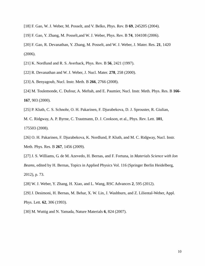
As previously mentioned, two different damage states have been investigated. Disorder
depth profiles extracted from RBS/C spectra are displayed in Fig. 1a for crystals that have been
irradiated to the highest Fe fluence prior to SHI irradiation. Complete amorphization is observed
in this damaged state, since the disorder fraction reaches the random level (i.e. fD=1) over a
thickness of approximately 50 nm (solid line in Fig.1a). After SHI irradiation (dashed and dotted
lines in Fig.1a), a decrease in thickness of the amorphous layer from the buried amorphous-
crystalline (a-c) interface is clearly evident. This finding suggests a recrystallization process.
TEM analysis (not shown here) confirms that the thickness of the amorphous layer decreased
after SHI irradiation, while no noticeable modification of the remaining amorphous region is
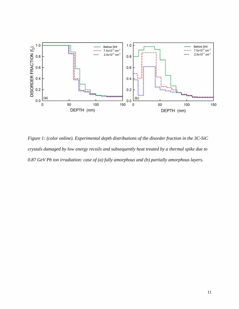
observed. The corresponding MD simulated amorphous layer (obtained after 70,000 recoils) is by
necessity thinner than the actual experimental layer, but is very similar in structure: a central
inner amorphous layer surrounded on each side by partially disordered interfacial layers that
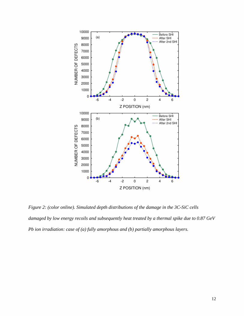
merge with the pristine, crystalline matrix. In this fully amorphous layer, the thermal spike is

6
found to induce recrystallization at the a-c interfaces, with minor additional recrystallization for a
second overlapped impact (Fig. 2a), consistent with experimental observations. This
recrystallization is illustrated in Fig. 3, where a section of the amorphous layer is shown before
and after the SHI energy is deposited as a thermal spike and allowed to relax.
For the samples irradiated to the lower Fe ion fluence, full amorphization is incomplete at
the damage peak (fD ~ 0.98) and, while a high degree of disorder is present over the entire
damaged thickness, some crystallinity remains (solid line in Fig. 1b). This structure is represented
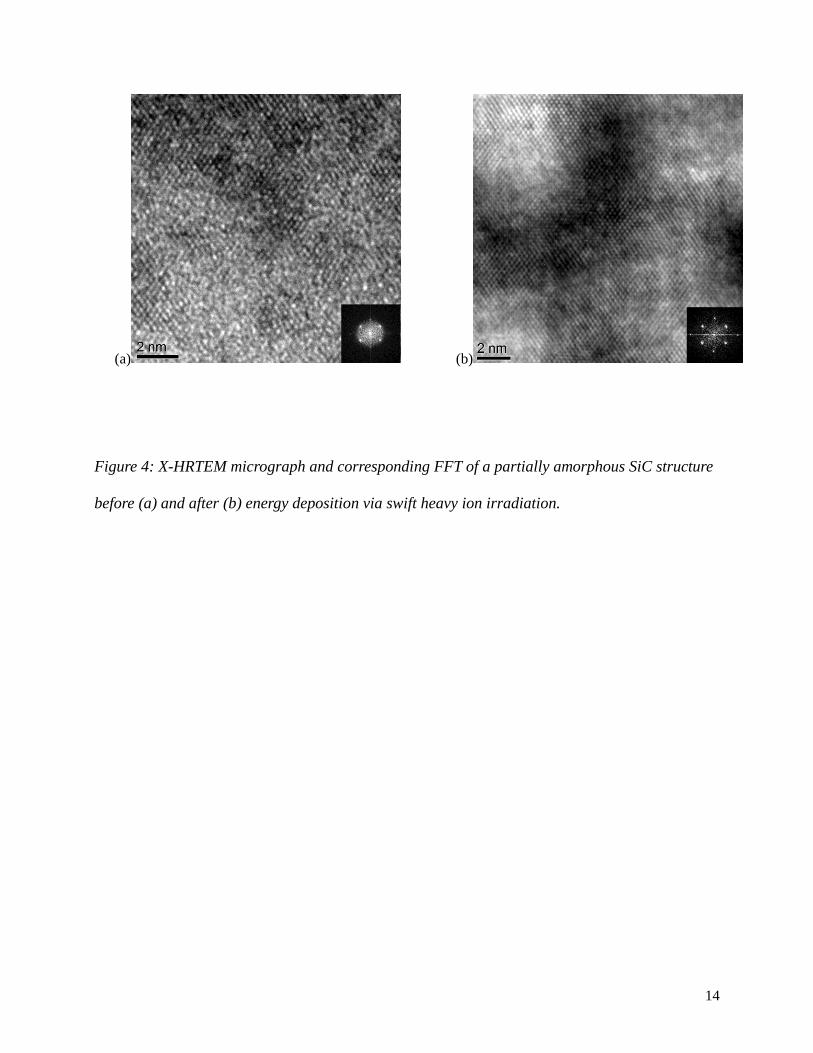
in Fig. 4a, which shows a high-resolution TEM image of the SiC crystal prior to SHI irradiation.
The image has been recorded in the vicinity of the damage peak (i.e. at a depth of ~25 nm), and it
shows a lattice with strongly disturbed (originally) crystalline regions which can be considered as
amorphous pockets. The corresponding FFT displayed in the inset supports this description. Upon
SHI, this partially amorphous structure behaves in a completely different manner than that
observed for fully amorphous crystals. Indeed, a decrease in fD over the whole damaged thickness
is readily evidenced after Pb ion irradiation (dashed and dotted lines in Fig. 1b), meaning that the
recovery is not only localized at the buried a-c interface (which is consistent with previous
results, see [6]). The observed recovery process is furthermore corroborated by high-resolution
TEM analysis. The initial damage state (Fig. 4a) contains substantial amorphous pockets;
however, following SHI irradiation, the amorphous pockets are clearly less numerous (Fig. 4b)
and have been superseded by disturbed, crystalline regions. The partial vanishing of the diffuse
scattering component in the FFT pattern, shown in inset of Fig. 4b, is consistent with this
interpretation. The corresponding MD partially amorphous layer (obtained after 30,000 recoils)
also shows significant recovery, within the central effective SHI track radius, over the whole
damaged thickness (Fig. 2b), in good agreement with the experimental results.
7
Despite the apparently different behavior between the two sets of experimental samples, it
is believed that the same recovery and recrystallization processes take place. In the fully
amorphous sample, recovery of point defects and recrystallization occurs primarily at the buried
a-c interface region, which TEM indicates (not shown here) to be rather coarse, leading to
sharpening of the disordered interface. A similar mechanism occurs in the partially amorphous
crystal, where crystalline areas are present over the entire damaged thickness. Consequently, it is
conjectured that discontinuous a-c interfaces act as seeds for recrystallization. Owing to the
exceptionally good agreement between experiments and simulations, it is very likely that the
observed damage recovery induced by swift heavy ions can, in fact, be explained by a thermal
spike annealing mechanism.
In conclusion, experimental and molecular dynamics simulation methods demonstrate that
room-temperature SHI irradiation induces recovery of pre-existing irradiation damage in SiC by a
thermal spike phenomenon. Considering that ion-beam-induced epitaxial crystallization (IBIEC),
which generally occurs with lower ion energy at temperatures above RT, has been previously
reported in semiconductors [27], insulators [28] or metal silicides [29], it is believed that the
room-temperature SHI induced recovery processes (SHIBIEC) reported here may also take place
in materials other than SiC. Thus, whether controlled in a laboratory or as a consequence of a
radiation environment, SHIBIEC may have beneficial healing effects on damaged structures.
Furthermore, it would be interesting to investigate the occurrence of this effect in chalcogenide
materials that are used in phase-change data-storage media [30]. Indeed, laser or electrical current
pulses are currently preferred to ion irradiation to induce local phase-changes because of a lack of
understanding of physical mechanisms occurring during ion irradiation; this lack is partially filled
in with the results presented in this Letter.
Acknowledgments
8
Authors from the CSNSM would like to warmly thank I. Monnet (CIMAP-Caen) for performing
SHI irradiations at Grand Accélérateur National d’Ions Lourds (GANIL) Caen, France.
W. J. Weber was supported by the U.S. Department of Energy, Basic Energy Sciences, Materials
Science and Engineering Division. The computational work used the supercomputer resources at
the National Energy Research Scientific Computing Center located at Lawrence Berkeley
National Laboratory, and the Newton computer cluster at the University of Tennessee.
References
9
[1] R. L. Fleischer, P. B. Price, and R. M. Walker, Science 149, 383 (1965).
[2] M. Toulemonde, W. Assmann, C. Dufour, A. Meftah, F. Studer, and C. Trautmann, Mat. Fys.
Medd. 52, 263 (2006).
[3] S. J. Zinkle, V. A. Skuratov, and D. T. Hoelzer, Nucl. Instrum. Meth. Phys. Res. B 191, 758
(2002).
[4] A. Benyagoub and A. Audren, Nucl. Instrum. Meth. Phys. Res. B 267, 1255 (2009).
[5] S. Sorieul, X. Kerbiriou, J.-M. Costantini, L. Gosmain, G. Calas, and C. Trautmann, J. Phys.:
Condens. Matter 24, 125801 (2012).
[6] A. Benyagoub, A. Audren, L. Thomé, and F. Garrido, Appl. Phys. Lett. 89, 241914 (2006).
[7] C. R. Eddy, Jr. and D. K. Gaskill, Science 324, 1398 (2009).
[8] F. Baletto and R. Ferrando, Rev. Mod. Phys. 77, 371 (2005).
[9] N. G. Wright and A. B. Horsfall, J. Phys. D: Appl. Phys. 40, 6345 (2007).
[10] Y. Katoh, L. L. Snead, I. Szlufarska, and W. J. Weber, Curr. Opin. Solid State Mater. Sci. 16,
143 (2012).
[11] E. D. Herderick and K. Cooper, Adv. Mater. Processes 170, 24 (2012).
[12] W. J. Weber, N. Yu and L. M. Wang, J. Nucl. Mater. 253, 53 (1998).
[13] A. Debelle, L. Thomé, D. Dompoint, A. Boulle, F. Garrido, J. Jagielski, D. Chaussende,
J. Phys. D: Appl. Phys. 43, (2010) 455408.
[14] L. Nowicki, A. Turos, R. Ratajczak, A. Stonert, and F. Garrido, Nucl. Instrum. Meth. Phys.
Res. B 240, 277 (2005).
[15] W. J. Weber and F. Gao, J. Mater. Res. 25, 2349 (2010).
[16] K. Nordlund, M. Ghaly, R. S. Averback, M. Caturla, T. Diaz de la Rubia, and J. Tarus, Phys.
Rev. B 57, 7556 (1998).
[17] F. Gao and W. J. Weber, Nucl. Instrum. Meth. Phys. Res. B 191, 504 (2002).
10
[18] F. Gao, W. J. Weber, M. Posselt, and V. Belko, Phys. Rev. B 69, 245205 (2004).
[19] F. Gao, Y. Zhang, M. Posselt,and W. J. Weber, Phys. Rev. B 74, 104108 (2006).
[20] F. Gao, R. Devanathan, Y. Zhang, M. Posselt, and W. J. Weber, J. Mater. Res. 21, 1420
(2006).
[21] K. Nordlund and R. S. Averback, Phys. Rev. B 56, 2421 (1997).
[22] R. Devanathan and W. J. Weber, J. Nucl. Mater. 278, 258 (2000).
[23] A. Benyagoub, Nucl. Instr. Meth. B 266, 2766 (2008).
[24] M. Toulemonde, C. Dufour, A. Meftah, and E. Paumier, Nucl. Instr. Meth. Phys. Res. B 166-
167, 903 (2000).
[25] P. Kluth, C. S. Schnohr, O. H. Pakarinen, F. Djurabekova, D. J. Sprouster, R. Giulian,
M. C. Ridgway, A. P. Byrne, C. Trautmann, D. J. Cookson, et al., Phys. Rev. Lett. 101,
175503 (2008).
[26] O. H. Pakarinen, F. Djurabekova, K. Nordlund, P. Kluth, and M. C. Ridgway, Nucl. Instr.
Meth. Phys. Res. B 267, 1456 (2009).
[27] J. S. Williams, G. de M. Azevedo, H. Bernas, and F. Fortuna, in Materials Science with Ion
Beams, edited by H. Bernas, Topics in Applied Physics Vol. 116 (Springer Berlin Heidelberg,
2012), p. 73.
[28] W. J. Weber, Y. Zhang, H. Xiao, and L. Wang, RSC Advances 2, 595 (2012).
[29] J. Desimoni, H. Bernas, M. Behar, X. W. Lin, J. Washburn, and Z. Liliental-Weber, Appl.
Phys. Lett. 62, 306 (1993).
[30] M. Wuttig and N. Yamada, Nature Materials 6, 824 (2007).
11
Figure 1: (color online). Experimental depth distributions of the disorder fraction in the 3C-SiC
crystals damaged by low energy recoils and subsequently heat treated by a thermal spike due to
0.87 GeV Pb ion irradiation: case of (a) fully amorphous and (b) partially amorphous layers.
12
Figure 2: (color online). Simulated depth distributions of the damage in the 3C-SiC cells
damaged by low energy recoils and subsequently heat treated by a thermal spike due to 0.87 GeV
Pb ion irradiation: case of (a) fully amorphous and (b) partially amorphous layers.
13
Figure 3: Atomistic model of the fully amorphous layer (a) before and (b) after the thermal spike.
The gray scale represents the structure factor of the atoms, i.e. the deviation from the zinc blende
bond angle. The cross-section is chosen from the area within the effective track recovery radius.
14
(a) (b)
Figure 4: X-HRTEM micrograph and corresponding FFT of a partially amorphous SiC structure
before (a) and after (b) energy deposition via swift heavy ion irradiation.


![A COMBINED EXPERIMENTAL AND … Paper/p107.pdfA COMBINED EXPERIMENTAL AND COMPUTATIONAL INVESTIGATION ON THE SYNTHESIS OF ACETALDEHYDE [CH 3CHO(X 1A0)] IN INTERSTELLAR ICES Chris J](https://img.pdfslide.us/doc/110x75/5e4490c81794884e045dcb8d/a-combined-experimental-and-paperp107pdf-a-combined-experimental-and-computational.jpg)