Embed Size (px)
Citation preview
1
CPEN 315 - Digital System Design
Combinational Logic Design
Chapter 3
© Logic and Computer Design Fundamentals, 4rd Ed., Mano
© 2008 Pearson Prentice Hall
Design Concepts and Automation
• A top-down design proceeds from an abstract, high-
level specification to a more and more detailed design
by decomposition and successive refinement
• A bottom-up design starts with detailed primitive blocks
and combines them into larger and more complex
functional blocks
• Designs usually proceed from both directions
simultaneously
– Top-down design answers: What are we building?
– Bottom-up design answers: How do we build it?
• Top-down controls complexity while bottom-up focuses
on the details
2
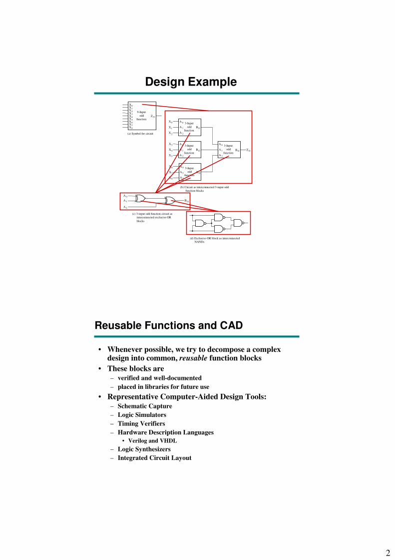
BO
X0X1X2X3X4X5X6X7X8
Z O
9-Input
odd
function
(a) Symbol for circuit
3-Input
odd
function
A 0
A 1
A 2
BO
3-Input
odd
function
A 0
A 1
A 2
BO
3-Input
odd
function
A 0
A 1
A 2
BO
3-Input
odd
function
A 0
A 1
A 2
X0
X1
X2
X3
X4
X5
X6
X7
X8
Z O
(b) Circuit as interconnected 3-input odd
function blocks
BO
A 0
A 1
A 2
(c) 3-input odd function circuit as
interconnected exclusive-OR
blocks
(d) Exclusive-OR block as interconnected
NANDs
Design Example
• Whenever possible, we try to decompose a complex design into common, reusable function blocks
• These blocks are
– verified and well-documented
– placed in libraries for future use
• Representative Computer-Aided Design Tools:
– Schematic Capture
– Logic Simulators
– Timing Verifiers
– Hardware Description Languages
• Verilog and VHDL
– Logic Synthesizers
– Integrated Circuit Layout
Reusable Functions and CAD
3
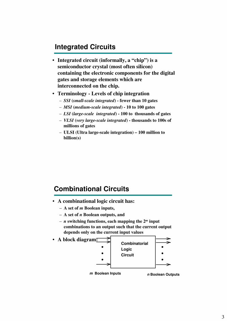
• Integrated circuit (informally, a “chip”) is a
semiconductor crystal (most often silicon)
containing the electronic components for the digital
gates and storage elements which are
interconnected on the chip.
• Terminology - Levels of chip integration
– SSI (small-scale integrated) - fewer than 10 gates
– MSI (medium-scale integrated) - 10 to 100 gates
– LSI (large-scale integrated) - 100 to thousands of gates
– VLSI (very large-scale integrated) - thousands to 100s of
millions of gates
– ULSI (Ultra large-scale integration) – 100 million to
billion(s)
Integrated Circuits
Combinational Circuits
• A combinational logic circuit has:
– A set of m Boolean inputs,
– A set of n Boolean outputs, and
– n switching functions, each mapping the 2m input
combinations to an output such that the current output
depends only on the current input values
• A block diagram:
m Boolean Inputsn Boolean Outputs
Combinatorial
Logic
Circuit

4
Simplification with
Don’t care conditions
There are applications in which the function is not
specified for certain input combinations:
- Input combinations never occur
- Input combinations are expected to occur but we simply
don’t care what the outputs are in response to the input
combinations.
These conditions can be used on a map to provide further
simplification of the function.
Simplification with
Don’t care conditions (example)
∑= )15,11,7,3,1(),,,( mDCBAF ''BACDF +=
DACDF '+=
x x
x x
xx
'' BACDF +=
∑= )15,11,7,3,1(),,,( mDCBAF
∑= )5,2,0(),,,( mDCBAd

5
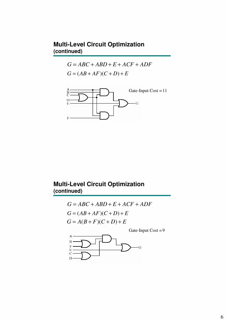
Multi-Level Circuit Optimization
Multi-Level circuits can reduce the cost of Combinational
Logic Circuits.
ADFACFEABDABCG ++++=
Gate-Input Cost = 17
Multi-Level Circuit Optimization (continued)
ADFACFEABDABCG ++++=
FDCAEDCABG )()( ++++=
Gate-Input Cost = 13
6
Multi-Level Circuit Optimization (continued)
EDCAFABG +++= ))((
ADFACFEABDABCG ++++=
Gate-Input Cost = 11
EDCAFABG +++= ))((
ADFACFEABDABCG ++++=
Multi-Level Circuit Optimization (continued)
EDCFBAG +++= ))((
Gate-Input Cost = 9
7
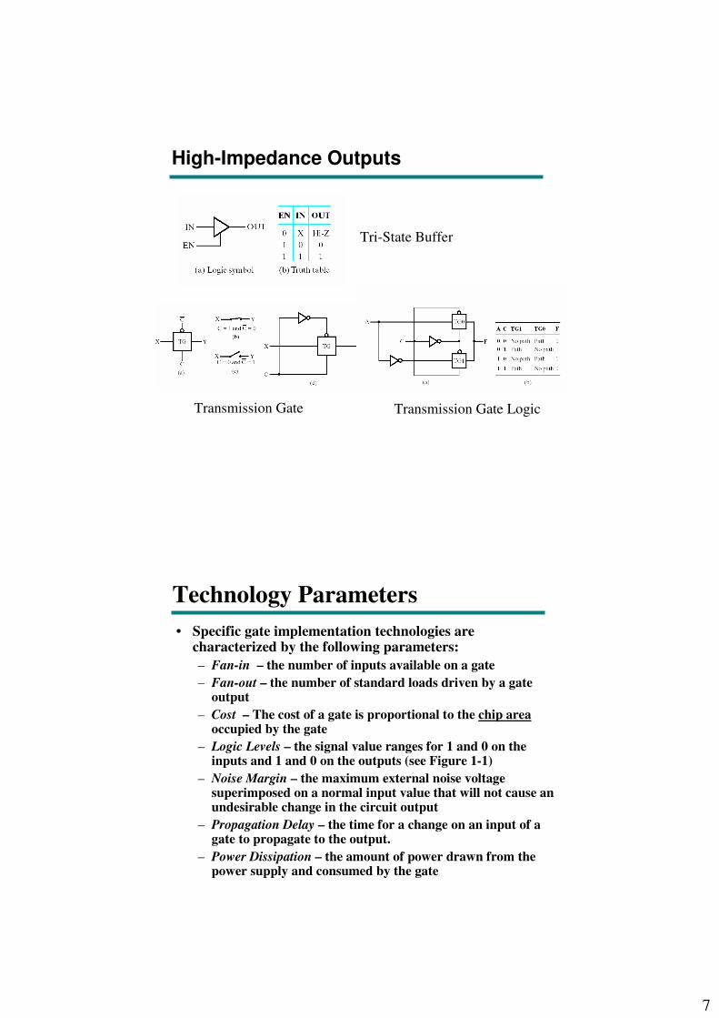
High-Impedance Outputs
Transmission Gate
Tri-State Buffer
Transmission Gate Logic
• Specific gate implementation technologies are characterized by the following parameters:
– Fan-in – the number of inputs available on a gate
– Fan-out – the number of standard loads driven by a gate output
– Cost – The cost of a gate is proportional to the chip areaoccupied by the gate
– Logic Levels – the signal value ranges for 1 and 0 on the inputs and 1 and 0 on the outputs (see Figure 1-1)
– Noise Margin – the maximum external noise voltage superimposed on a normal input value that will not cause an undesirable change in the circuit output
– Propagation Delay – the time for a change on an input of a gate to propagate to the output.
– Power Dissipation – the amount of power drawn from the power supply and consumed by the gate
Technology Parameters

8
Propagation Delay
• Propagation delay is the time for a change on an input
of a gate to propagate to the output.
• Delay is usually measured at the 50% point with
respect to the H and L output voltage levels.
• High-to-low (tPHL) and low-to-high (tPLH) output signal
changes may have different propagation delays.
• High-to-low (HL) and low-to-high (LH) transitions are
defined with respect to the output, not the input.
• An HL input transition causes:
– an LH output transition if the gate inverts and
– an HL output transition if the gate does not invert.
in Chapter 6
Propagation Delay (continued)
• A logic gate always takes some time to change states
• tPLH is the delay time before output changes from low to high
• tPHL is the delay time before output changes from high to low
• both tPLH & tPHL are measured between the 50% points on the
input and output transitions
tPHL tPLH
INPUT
OUTPUT
50%
tpd = max (tPHL, tPLH)
9
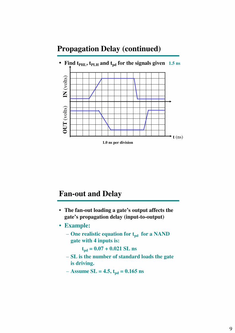
• Find tPHL, tPLH and tpd for the signals givenIN
(volt
s)O
UT
(volt
s)
t (ns)1.0 ns per division
Propagation Delay (continued)
1.5 ns
Fan-out and Delay
• The fan-out loading a gate’s output affects the
gate’s propagation delay (input-to-output)
• Example:
– One realistic equation for tpd for a NAND
gate with 4 inputs is:
tpd = 0.07 + 0.021 SL ns
– SL is the number of standard loads the gate
is driving.
– Assume SL = 4.5, tpd = 0.165 ns
10
Fan-out and Delay - example
• A 4-input NAND gate is attached to the inputs of the
following gates with a given number of standard loads
representing their inputs:
– 4-input NOR gate (0.8 standard load)
– 3-input NAND gate (1.00 standard load)
tpd = 0.07 + 0.021 SL ns (4-input NAND gate)
– What is the total tpd?
Note that in modern high-speed designs, the
portion of gate delay due to wiring capacitance is
often significant.
0.11 ns
Fan-in
• For high-speed technologies fan-in, the number
of inputs to a gate is often restricted to no more
than 4 or 5.
• Problem: Implement a 7-input NAND gate
using NAND gates with 4 inputs.
11
Cost
• In an integrated circuit:
– The cost of a gate is proportional to the chip
area occupied by the gate
– The gate area is roughly proportional to the
number and size of the transistors and the
amount of wiring connecting them
• If the actual chip area occupied by the gate is
known, it is a far more accurate measure.
Speed-Power Product
• Speed (propagation delay) and power consumption are the
two most important performance parameters of a digital IC.
• A simple means for measuring and comparing the overall
performance of an IC family is the speed-power product
(the smaller, the better).
• For example, an IC has
– an average propagation delay of 10 ns and
– an average power dissipation of 5 mW.
– What is the speed-power product ? 50 pico joules
12
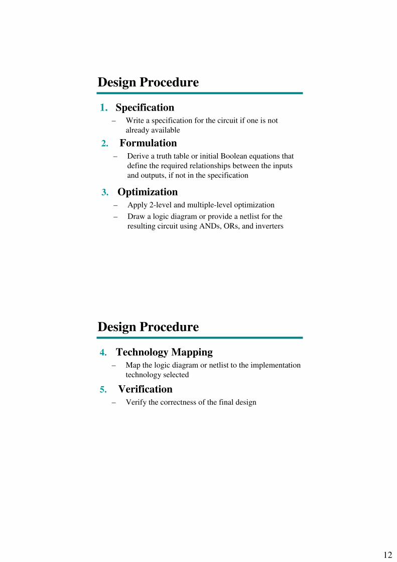
Design Procedure
1. Specification
– Write a specification for the circuit if one is not
already available
2. Formulation
– Derive a truth table or initial Boolean equations that
define the required relationships between the inputs
and outputs, if not in the specification
3. Optimization
– Apply 2-level and multiple-level optimization
– Draw a logic diagram or provide a netlist for the
resulting circuit using ANDs, ORs, and inverters
4. Technology Mapping
– Map the logic diagram or netlist to the implementation
technology selected
Design Procedure
5. Verification
– Verify the correctness of the final design

13
Design Example
1. Specification– BCD to Excess-3 code converter
– Transforms BCD code for the decimal digits to Excess-3 code for the decimal digits
– BCD code words for digits 0 through 9: 4-bit patterns 0000 to 1001, respectively
– Excess-3 code words for digits 0 through 9: 4-bit patterns consisting of 3 (binary 0011) added to each BCD code word
– Implementation:
• multiple-level circuit
• NAND gates (including inverters)
Design Example (continued)
2. Formulation
– Conversion of 4-bit codes can be most easily
formulated by a truth table
– Variables
- BCD:
A,B,C,D
– Variables
- Excess-3
W,X,Y,Z
– Don’t Cares
- BCD 1010
to 1111
Input BCD
A B C D
Output Excess-3
WXYZ
0 0 0 0 0 0 1 1 0 0 0 1 0 1 0 0 0 0 1 0 0 1 0 1 0 0 1 1 0 1 1 0 0 1 0 0 0 1 1 1 0 1 0 1 1 0 0 0 0 1 1 0 1 0 0 1 0 1 1 1 1 0 1 0 1 0 0 0 1 0 1 1 1 0 0 1 1 0 1 1
14
B
C
D
A
0 1 3 2
4 5 7 6
12 13 15 14
8 9 11 10
1
11
1
X X X
X X
X
1
B
C
D
A
0 1 3 2
4 5 7 6
12 13 15 14
8 9 11 10
1
11
1
X X X
X X
X
1
B
C
D
A
0 1 3 2
4 5 7 6
12 13 15 14
8 9 11 10
1 1
1
1
X X X
X X
X
1
B
C
D
A
0 1 3 2
4 5 7 6
12 13 15 14
8 9 11 10
1 1
1
X X X
X X
X
1
1
w
z y
x
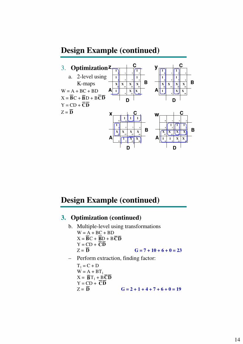
3. Optimization
a. 2-level using
K-maps
W = A + BC + BD
X = C + D + B
Y = CD +
Z =
B CDB
CD
D
Design Example (continued)
3. Optimization (continued)
b. Multiple-level using transformationsW = A + BC + BD
X = C + D + B
Y = CD +
Z = G = 7 + 10 + 6 + 0 = 23
– Perform extraction, finding factor:
T1 = C + D
W = A + BT1
X = T1 + B
Y = CD +
Z = G = 2 + 1 + 4 + 7 + 6 + 0 = 19
B CDB
CD
D
B CD
CD
D
Design Example (continued)

15
3. Optimization (continued)
b. Multiple-level using transformations
T1 = C + D
W = A + BT1
X = T1 + B
Y = CD +
Z = G = 19
– An additional extraction not shown in the text since it uses a
Boolean transformation: ( = C + D = ):
W = A + BT1
X = T1 + B
Y = CD +
Z = G = 2 +1 + 4 + 6 + 4 + 0 = 16
B CD
CD
D
B T1
D
T1
CD T1
Design Example (continued)
4. Technology Mapping• Mapping with a library containing inverters and 2-input NAND,
2-input NOR, and 2-2 AOI gates A
B
C
D
W
X
Y
Z
A
B
CD
W
X
Y
Z
Design Example (continued)
16
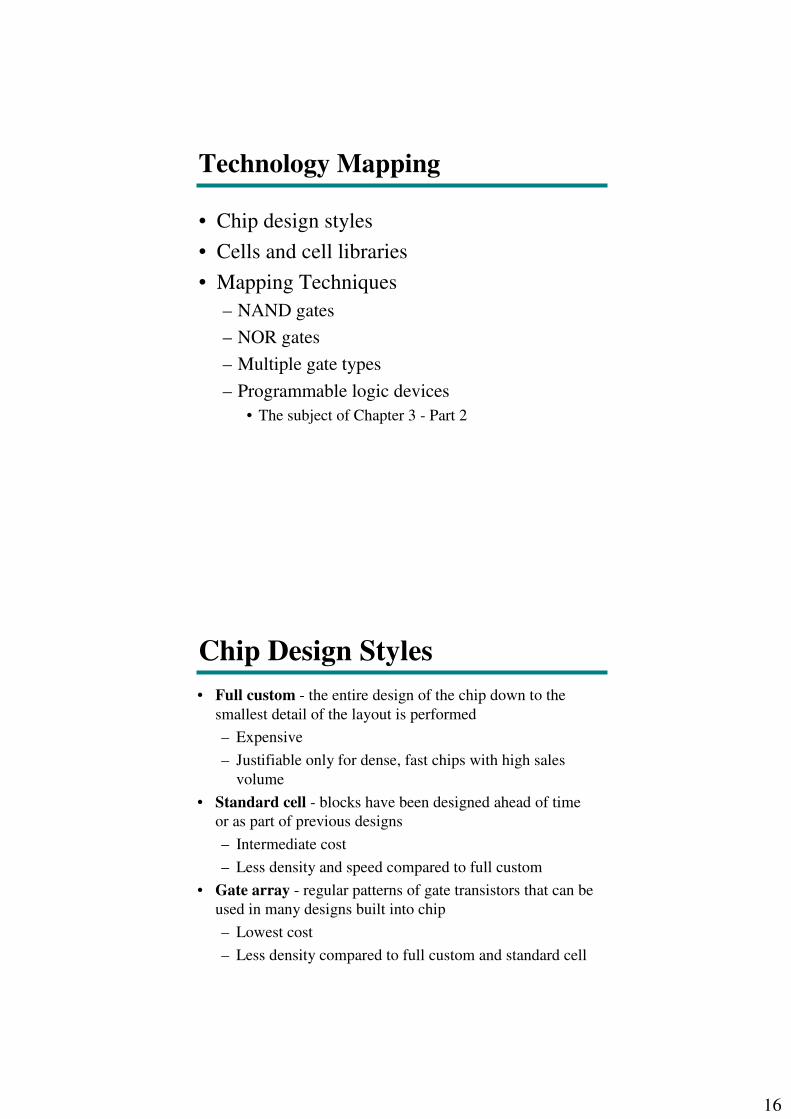
• Chip design styles
• Cells and cell libraries
• Mapping Techniques
– NAND gates
– NOR gates
– Multiple gate types
– Programmable logic devices
• The subject of Chapter 3 - Part 2
Technology Mapping
• Full custom - the entire design of the chip down to the
smallest detail of the layout is performed
– Expensive
– Justifiable only for dense, fast chips with high sales
volume
• Standard cell - blocks have been designed ahead of time
or as part of previous designs
– Intermediate cost
– Less density and speed compared to full custom
• Gate array - regular patterns of gate transistors that can be
used in many designs built into chip
– Lowest cost
– Less density compared to full custom and standard cell
Chip Design Styles

17
• Cell - a pre-designed primitive block
• Cell library - a collection of cells available for
design using a particular implementation
technology
• Cell characterization - a detailed specification of
a cell for use by a designer - often based on actual
cell design and fabrication and measured values
• Cells are used for gate array, standard cell, and in
some cases, full custom chip design
Cell Libraries
Cell
Name
Cell
Schematic
Normalized
Area
TypicalInput
Load
TypicalInput-to-Output
Delay
BasicFunction
Templates
Inverter 1.00 1.000.04
+ 0.012 x SL
2NAND 1.25 1.000.05
+ 0.014 x SL
2NOR 1.25 1.000.06
+ 0.018 x SL
2-2 AOI 2.25 0.950.07
+ 0.019 x SL
Example Cell Library
18
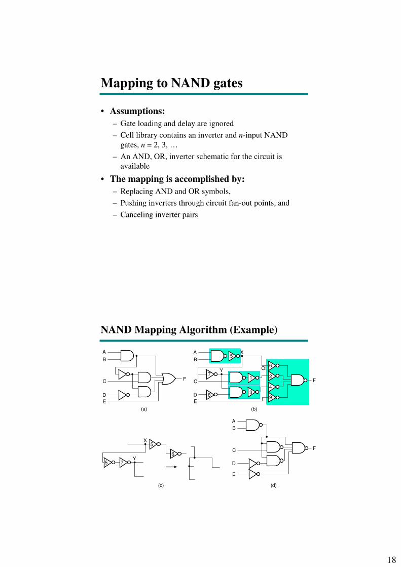
• Assumptions:
– Gate loading and delay are ignored
– Cell library contains an inverter and n-input NAND
gates, n = 2, 3, …
– An AND, OR, inverter schematic for the circuit is
available
• The mapping is accomplished by:
– Replacing AND and OR symbols,
– Pushing inverters through circuit fan-out points, and
– Canceling inverter pairs
Mapping to NAND gates
A
B
C
D
F
E
(a)
A
B
C
7
5
1
6
2
4
9
X
Y
38D
E
F
(b)
A
B
C
D
E
F
(d)
X
5
5
7
6Y
(c)
OI
NAND Mapping Algorithm (Example)
19
A
B
C
D
E
F
(c)
F
A
B
X
C
D
E(b)
A
B
C
D
E
F
(a)
2
3
1
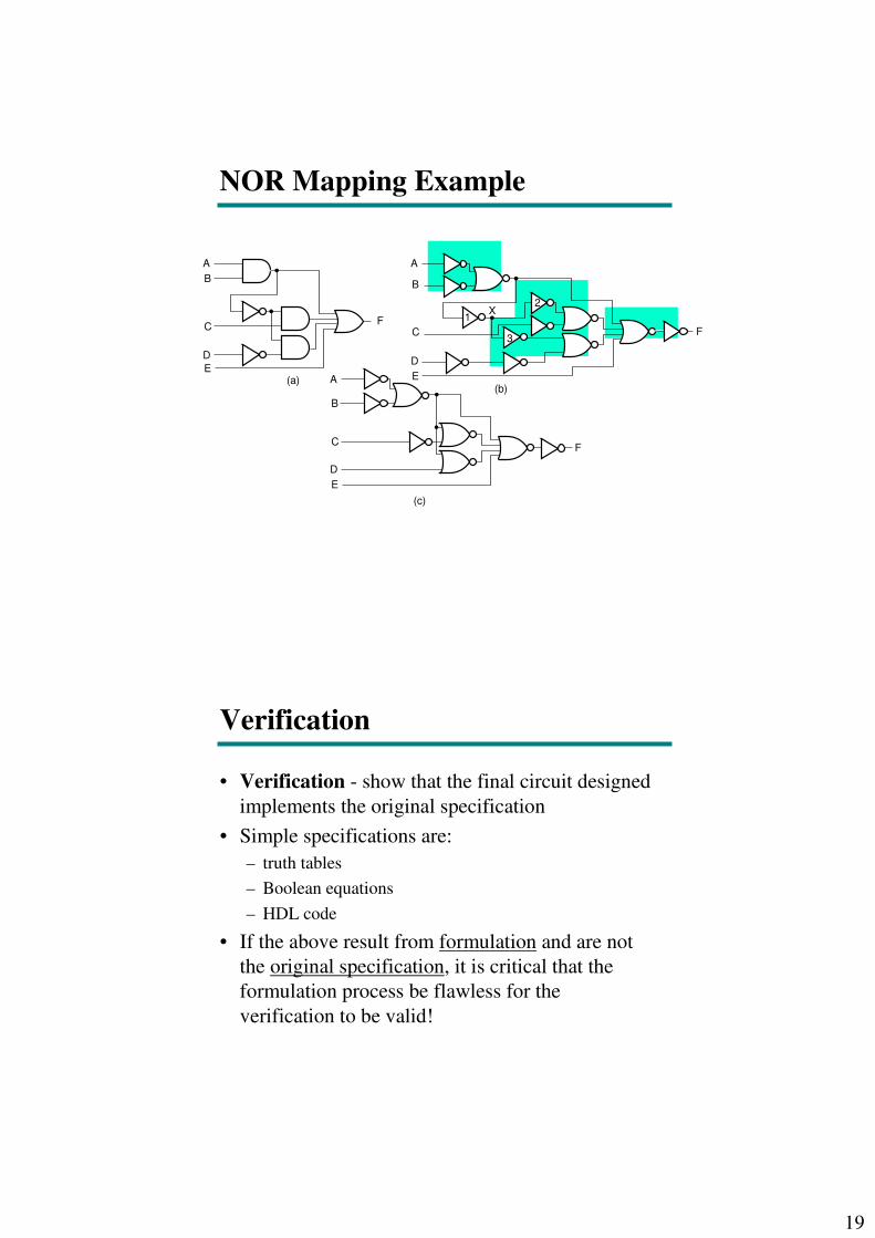
NOR Mapping Example
• Verification - show that the final circuit designed
implements the original specification
• Simple specifications are:
– truth tables
– Boolean equations
– HDL code
• If the above result from formulation and are not
the original specification, it is critical that the
formulation process be flawless for the
verification to be valid!
Verification
20
• Manual Logic Analysis
– Find the truth table or Boolean equations for the final circuit
– Compare the final circuit truth table with the specified truth table,
or
– Show that the Boolean equations for the final circuit are equal to
the specified Boolean equations
• Simulation
– Simulate the final circuit (or its netlist, possibly written as an
HDL) and the specified truth table, equations, or HDL description
using test input values that fully validate correctness.
– The obvious test for a combinational circuit is application of all
possible “care” input combinations from the specification
Basic Verification Methods
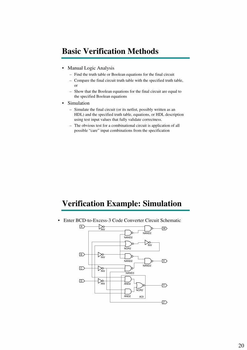
• Enter BCD-to-Excess-3 Code Converter Circuit Schematic
NAND2
NAND2
INV
NOR2
INV
NAND2
INV
NAND2
AND2
AND2
NAND3INV
INV
NOR2
W
B
A
C
D
X
AOI
Y
Z
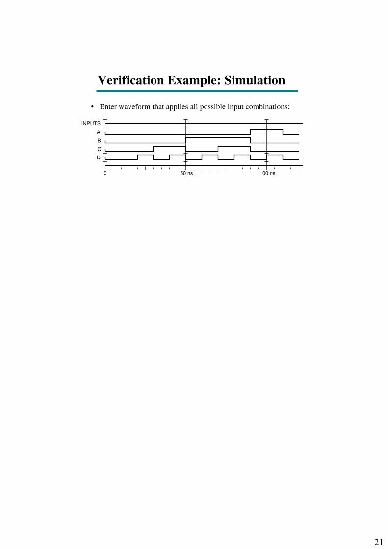
Verification Example: Simulation
21
• Enter waveform that applies all possible input combinations:
0 50 ns 100 ns
INPUTS
A
B
C
D
Verification Example: Simulation