Embed Size (px)
Citation preview
ORDER No.AD0211153C3
Portable MD Player
SJ-MJ55GHColour
(S)...................Silver Type
SPECIFICATIONS
Specifications

AudioSystem: MiniDisc digital audio systemBeam source: Semiconductor laserWave length: 780 nmSampling frequency: 44.1 kHzCoding: Adaptive Transform Acoustic
Coding (ATRAC/ ATRAC3)No. of channels: 2 (left and right, stereo)
1 (monaural)Frequency response: 20 Hz~20 kHz (+0 dB, -6dB)Wow and flutter: Below measurable limit
GeneralHeadphones:
Output level (approx.): 3.0 mW+3.0 mWInpedance (approx.): 32
Speakers (ceramic card type):Output level (approx.): 45 mW+45 mWInpedance (approx.): 200 / 1kHz
Power supplyRechargeable battery: DC 1.2V
(included rechargeable battery)Battery: DC 1.5V (One LR6, AA, UM-3 battery)
Dimensions (WxHxD)Cabinet dimensions: 79.9x72.7x14.1 mmincl.projecting parts: 80.9x74.2x17.0 mm
Weights: 96 g (with battery)69 g (without battery)
Play time[Approximate operating time in hours (in hold mode, at 25°C, on a flat, stable surface)]
Battery type: Play time (Stereo/ LP2/ LP4)Rechargeable: 40 hours/ 53 hours/ 70 hoursPanasonic alkaline: 63 hours/ 93 hours/ 121 hoursBoth together: 103 hours/ 148 hours/ 193 hours
[When the rechargeable battery (included) is fully recharged.]
AC adaptor and chargerAC adaptor input: AC220 V, 50/60 Hz, 5 VAAC adaptor output and Charger input:
DC 3.5 V, 0.5A
Charger output: DC 2V, 0.5 ARecharging time: About 3.5 hours

Notes:- The play time may be less depending on the operating
conditions.- Specifications are subject to change without notice. Weight
and dimensions are approximate.
2002 Matsushita Electric Industrial Co., Ltd. All rights reserved. Unauthorized copying and distribution is a violation of law.
1. Accessories- Stereo earphones...................................................1 pc. /
(L0BAB0000174)- Wired remote control..............................................1 pc. /
(N2QCBD000020)- External battery case..............................................1 pc. /
(K3ZZ00200038)- Nickel-metal hydride rechargeable battery.............1 pc. /
(RFKFFAZ01EM1)- Soft case.................................................................1 pc. / (RFC0074-H)- Speaker/Battery charger............................................1 pc. /
(L0EAAB000011)- AC adaptor...............................................................1 pc. /
(N0JCBD000001)
2. Precaution of Laser Diode

3. Operating Instructions4. Handling Precautions for MD Mechanism (Optical pickup)The laser diode in the MD mechanism (optical pickup) may break down due to potential difference caused by static electricity of clothes or human body.So, be careful of electrostatic breakdown during repair of the traverse deck (optical pickup).
4.1. Handling the MD mechanism (optical pickup)1. The MD mechanism (optical pickup) is an extremely high-
precision construction and must not be subjected to impact, excessive vibration, or other types of rough handling.
2. In order to prevent static electricity damage to the laser diode, use a short pin or similar tool to short the optical pickup’s flexible circuit boards after they have been disconnected from the main circuit board. (as shown in Fig. 1 )
3. Handle the flexible circuit boards with care; excessive force could cause them to be broken.
4. Do not turn the pre-set variable resistor (for adjustment of the laser power); it has been adjusted at the factory.(as shown in Fig. 2 )
Fig. 1

Fig. 2
4.2. Grounding for electrostatic breakdown prevention1. Human body grounding
Use the anti-static wrist strap to discharge the static electricity from your body. (as shown in Fig. 3 )
2. Work table groundingPut a conductive material (sheet) or steel sheet on the area where the traverse deck (optical pickup) is placed, and ground the sheet. (as shown in Fig. 4 )
CautionThe static electricity of your clothes will not be grounded through the wrist strap.So, take care not to let your clothes touch the traverse deck (optical pickup).
Fig. 3

Fig. 4
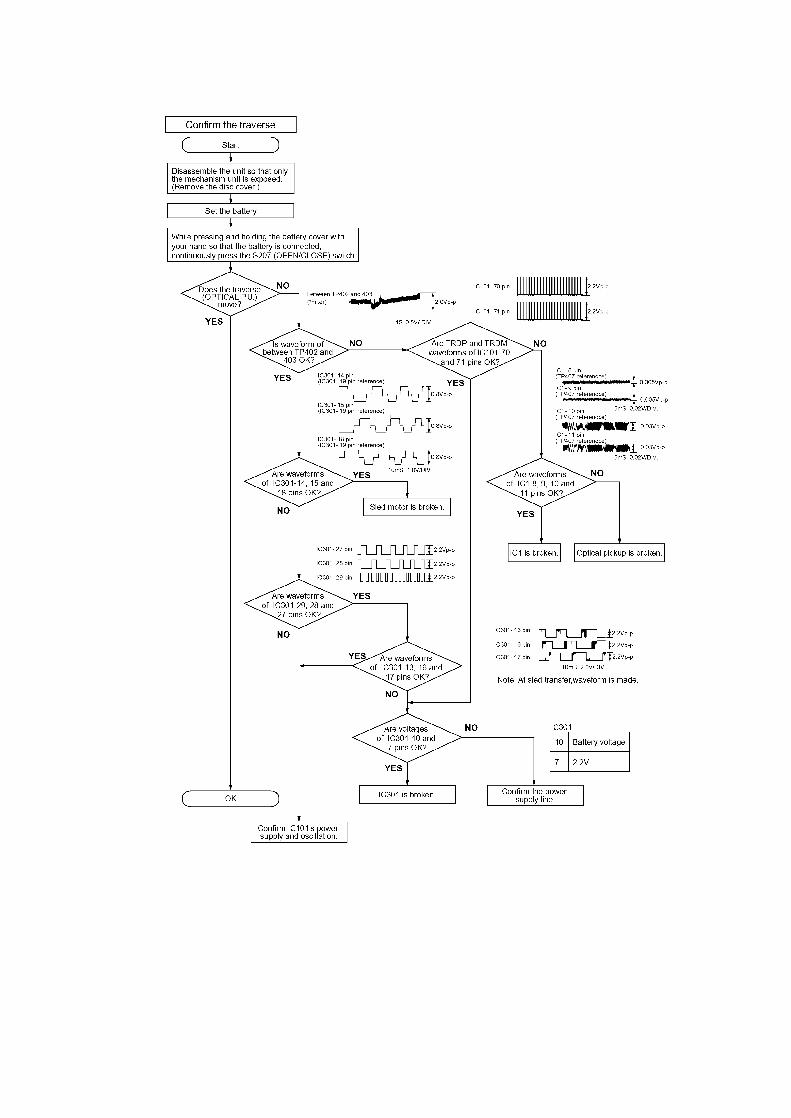
5. Operation Checks and Component Replacement Procedures- This section describes procedures for checking the operation of
the major printed circuit boards and replacing the main components.
- For reassembly after operation checks or replacement, reverse the respective procedures. Special reassembly procedures are described only when required.
- After replacing the main components (optical pickup or traverse motor, etc.) of mechanism unit block, change to the adjust mode, and then perform the adjustments (Laser power, off-set, ROM/RAM).
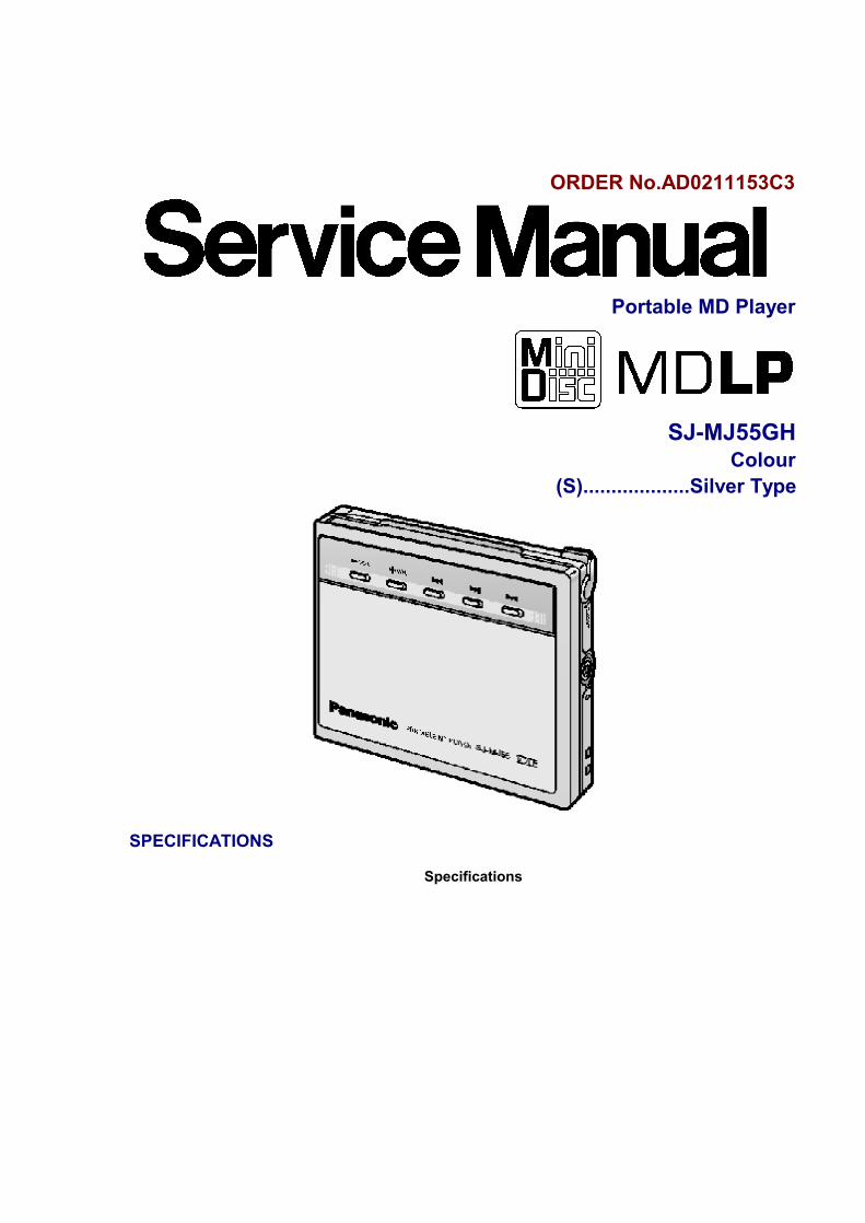
5.1. Checking for the P.C.B.
- Check the P.C.B. as shown below.

5.2. Replacement for the intermediate cabinet- Follow the (Step1)-(Step3) of item 5.1.

5.3. Replacement for the disk cover ass’y and the link units (L), (R)- Follow the (Step1)-(Step3) of item 5.1.- Follow the (Step1)-(Step4) of item 5.2.

5.4. Replacement for the traverse motor- Follow the (Step1)-(Step3) of item 5.1.

5.5. Replacement for the optical pickup- Follow the (Step1)-(Step3) of item 5.1.- Follow the (Step1)-(Step5) of item 5.4.


6. Measurements and AdjustmentsNote:After replacing the main components (optical pickup, traverse motor, IC201, IC202 or P.C.B. ass’y, etc.) of mechanism unit block, change to the adjust mode, and then perform the “Laser power adjustment”, “Off-setautomatic adjustment” and “Playback-only disc/magneto-optical disc automatic adjustment”.
6.1. Instruments to prepare1. Playback-only disc (Test disc RFKV0006)2. Commercially available recordable disc (fully recorded with
music) (magneto-optical disc)3. Laser power meter (LE8010 or compatible meter)4. Remote controller (Parts No: N2QCBD000020) [or Remote
controller of SJ-MJ88 etc. (Parts No: RFEV025P-SM)]
6.2. Laser power adjustment, Off-set automatic adjustment, Playback-only disc/magneto-optical disc automatic adjustment magnet6.2.1. Enter the adjustment mode
Note:For use of MD cartridge type laser power meter, disassemble this unit into the state of only the mechanism unit before perform the laser power adjustment (as for the method of disassembly, refer to “5.2. Replacement for the intermediatecabinet”).

1. Set the battery and connect the remote controller. (The position of the HOLD switch of remote controller is “OFF”.)
2. Turn off the power, and switch main unit’s HOLD switch off.3. Press the VOL+( ), VOL-( ), ( ), and ( )keys on the
remote controller within two seconds. (asshown in Fig. 5 )Fig. 5
4. When the adjustment mode is activated, “T0E ” will be displayed on the LCD of remote controller. After “T0E ” is displayed, select the desired adjustment item with the button or button of the remote controller. (If it is not displayed, perform the procedures written above again.)
*In the display of T0E ~ TFE shown above, you must adjust T0E , T1E , T2E and T3E . You must perform the adjustment by observing the order T0E T1E T2E T3E .
Note:If it is going to perform “T2E” and “T3E”, without performing “T1E”, it will be displayed as “NG”.If it is going to perform “T3E” when “T2E” is “NG”, it will be displayed as “NG”.

6.2.2. Laser Power AdjustmentAdjust each laser power: read power for reading (play).6.2.2.1. Set the Unit to the Adjustment Mode
CautionsAbout handling the optical pickup and the magnetic head.
- The optical pickup is structured precisely; therefore, it is very fragile. Be careful not to touch it with the edge of the laser power meter. Do not touch the lens.
- The sensor of the laser power meter is a very fine part. Be careful not to touch it to the optical pickup lens.
- The focus point of the laser reaches to 356°F. Therefore, avoid adjusting using laser power for a long time because the sensor of the laser power meter may be burned.
- Do not set the unit to the laser power adjustment mode with the MD loaded. Doing so may result in damage to the MD.
- Laser diode in the optical pickup may be destroyed by the static electricity generated in your clothes or body. Be especially careful with the static electricity.
6.2.2.2. Adjustment Procedure
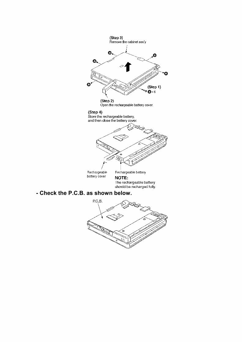
1. Have “T0**” indicated on display, and move the optical pickup to the most inside (only when a MD cartridge type laser power meter is used).
2. Set the laser power meter.[For use of stick type laser power meter.]2-1 Uncover the laser power meter (as shown in Fig. 6 ).2-2 Locate the sensor of the laser power meter right over above the optical pickup (horizontally at a level of the disc position). (as shown in Fig. 7 )[For use of MD cartridge type laser power meter.]2-1 Open the shutter of the laser power meter. (as shown in Fig. 9 )2-2 Set the laser power meter. (as shown in Fig. 8 )
Fig. 6

3. Press the key of the remote controller (“T0E ” changes to “LD ” of the LCD).
4. Press the key of the remote controller (“LD ” changes to “LP ” of the LCD).
5. Set the laser power at 600 W±10% by using VOL+ and VOL- key of the remote controller. / [Specified range: 600 W±10%]Caution:Proceeding on to the subsequent adjustment procedure with the read power exceeding “over 660 W” will result in damage to the optical pickup.
6. Set the laser power with the key of the remote controller (“LP ” changes to “LDOK ” in the LCD).
7. Press the key of the remote controller (“LDOK ” changes to “T0E ” on the LDC.
8. Remove the laser power meter. Laser power adjustment is finished.
<Stick type>Fig. 7
<MD cartridge type>Fig. 8
[How to open the shutter]
1. Insert a thin and hard card to the crevice between laser power meter, and pull a card in the direction of an arrow (1).
2. A stopper moves in the direction of an arrow (2).3. Move the shutter in the direction of an arrow (3) and the shutter
opens.
Caution:Please be sure to shut the shutter after the adjustment end.
Fig. 9

6.2.3. Off-set automatic adjustment
1. With “T1E ” displayed, leave the disc cover open.2. Pressing the key on the remote controller will start
adjustment.3. During adjustment, “FADJ ” is displayed on the LCD of the remote
controller. If there is no abnormality, “FOK ” will be displayed.4. Pressing the key while “FOK ” is displayed will return to the
“T1E ” display mode.
6.2.4. Magneto-optical disc automatically adjustment
1. Have “T2E ” indicated on display, and set the full-recorded magneto-optical disc. (Check to make sure the disc is properly seated.)
2. Press key of the remote controller. The adjustment is started.
3. During adjustment, “AADJ ” is displayed on the LCD of the

remote controller. / If there is no abnormality, “AOK ” will be displayed.
Note:If it is displayed “ANG ”, check “7. Troubleshooting Guide” in the order.
4. Press key (“AOK ” or “ANG ” changes to “T2E ”).5. After the adjustment is finished, remove the disc.
6.2.5. Playback-only disc automatic adjustment
1. Have “T3E ” indicated on display, set the playback-only disc. / (Check to make sure the disc is properly seated.)
2. Press key of the remote controller. The adjustment is started.
3. During adjustment. “AADJ ” is displayed on the LCD of the remote controller. / If there is no abnormality, “AOK ” will be displayed.
Note:If it is displayed “ONG ”, check “7. Troubleshooting Guide” in the order.
4. Press key (“OOK ” or “ONG ” changes to “T3E ”).5. After the adjustment is finished, remove the disc.
6.2.6. How to get out the adjustment modeRemove the battery when you finish the adjustment.
6.3. Checking the main unit's keys1. Set the battery and connect the remote controller.2. Turn off the power, and switch main unit’s HOLD switch ON. 3. Press the VOL+( ), VOL-( ), ( ), and ( ) keys on the
remote controller within two seconds. (asshown in Fig. 5 )4. When the unit enters the unit key check mode, the display shows
“E KEX ”. While “E KEX ” is displayed, press the , , , VOL+, VOL- and HOLD keys of the unit. / *When the first key is pressed, the display will change to “E ”.

Main unit’s keys LCD display position and lettersAfter the second key is pressed, the first digit displayed will change from “ ” to “O ”.HOLD OFF
VOL+ After the second key is pressed, the second digit displayed will change from “ ” to “O ”.VOL-After the second key is pressed, the third digit displayed will change from “ ” to “O ”.
5. After all keys have been pressed and there is no abnormality, “E OOO ” will be displayed.
6. Perform below voltage check about the keys come under if it is not displayed “E OOO ”.
Main unit’s keys Check points ON OFFIC201 48pin 0V 2.2V
HOLD TP428 0V 2.2VVOL+ TP421 0V 2.2VVOL- TP421 0.58V 2.2V
TP421 1.13V 2.2VTP421 1.69V 2.2V
Note:Refer to “12. Printed Circuit Board Diagram” for the test points.
7. Remove the battery when you exit from this mode.
7. Troubleshooting Guide


8. Precaution for Replacement of EEPROM IC (IC202) and SYSTEMCONTROL IC (IC201)8.1. Replacement of EEPROM IC (IC202)In case of replacing EEPROM IC (IC202), depending on the Parts No. of SYSTEMCONTROL (IC201), it is need to replace SYSTEMCONTROL simultaneously.For details, please refer to the following table.
Parts No. of SYSTEMCONTROL (IC201) ReplacementMN101C32GAG1 NeedMN101C32GAG2 Needlessness
NoteWhen “MN101C32GAG1” is mounted, please exchange for “MN101C32GAG2”.
8.2. Replacement of SYSTEMCONTROL IC (IC201)Exchange only SYSTEMCONTROL IC (IC201).
CautionAfter replacing either “IC201” or “IC202”, please be sure to perform the “laser power adjustment”, “Off-set automatic adjustment” and “Playback only disc/magneto-opticaldisc automatic adjustment”. (Refer to “6 Measurements and Adjustments ”)If the set is operated without adjusting, an error will be displayed and the set will not operate.
9. Precaution for Replacement of P.C.B. ASS’Y

After replacing P.C.B. ASS’Y, please be sure to perform the “laser power adjustment”, “Off-set automatic adjustment” and “Playback only disc/magneto-optical disc automatic adjustment”.(Refer to “6 Measurements and Adjustments ”)If the set is operated without adjusting, an error will be displayed and the set will not operate.
10. Schematic Diagram Notes10.1. Type Illustration of IC's, Transistors and Diodes
10.2. Schematic Diagram NotesThis schematic diagram may be modified at any time with the development of new technology.
Notes:
S207
: Cover open/close det. switch
S208
: Hold switch in “OFF” position. (HOLD)
SX201
: Volume control switch (-)
SX202
: Volume control switch (+)
SX203
: Skip/search switch ( )
SX204
: Skip/search switch ( )
SX206
: Play/stop switch ( )
- Indicated voltage values are the standard values for the unit measured by the DC electronic circuit tester (high-impedance) with the chassis taken as standard. Therefore, there may exist some errors in the voltage values, depending on theinternal impedance of the DC circuit tester.
No mark: MD STOP( ): MD play [1kHz, L+R, 0dB] (*) (*) The play of MD is performed in “Jitter measurement / (T4E)” mode. (Refer to “6.2.1. Enter the adjustment mode ” for the / method of going into “Jittermeasurement (T4E) mode”).
Important safety notice:Components identified by mark have special characteristics important for safety.Furthermore, special parts which have purpose of fire-retardant (resistors), high-quality sound (capacitors), low-noise (resistors), etc. are used. When replacing any of components, be sure to use only manufacture's specified parts shown in theparts list.
Caution!IC and LSI are sensitive to static electricity.

Secondary trouble can be prevented by taking care during repair.Cover the parts boxes made of plastics with aluminum foil.Ground the soldering iron.Put a conductive mat on the work table.Do not touch the legs of IC or LSI with the fingers directly.
Voltage and signal line: Positive voltage line: Playback signal line
11. Schematic Diagram12. Printed Circuit Board Diagram13. Block Diagram14. Terminal Function of IC’s14.1. IC1 (C1BB00000728): RF AMP
Pin No.
Mark I/O Division
Function
1 NC — Not used, open2 RVCC I Power supply input
terminal3 RF1 I RF 1 signal input terminal4 RF2 I RF 2 signal input terminal5 VCC I Power supply input
terminal6 F1 I F 1 signal input terminal7 F2 I F 2 signal input terminal8 A I A signal input terminal9 B I B signal input terminal10 C I C signal input terminal11 D I D signal input terminal12 GHSW I ROM/ RAM gain switching
signal input terminal13 BWCT I Wobble signal band pass
filter switcing input terminal

Pin No.
Mark I/O Division
Function
14 SETR I Band pass filter control input terminal
15 GND — GND terminal16 LDO O APC output terminal17 LDS I I/V converted laser quantity
of light input terminal18 LDREF I Laser control signal input
terminal19 VC O 1/2VCC (reference voltage)
output terminal20 VR I Connected to GND through
capacitor21 WOO O Wobble signal output
terminal22 CC O C signal dark-side detection
/ amplified output terminal23 DD O D signal dark-side detection
/ amplified output terminal24 BB O B signal IV conversion
output terminal25 AA O A signal IV conversion
output terminal26 FF2 O F2 signal IV conversion
output terminal27 FF1 O F1 signal IV conversion
output terminal28 RGND — GND terminal29 BOTTOM — RF bottom signal output
terminal (Not used, open)
30 PEAK O RF peak signal output terminal
31 HFL O Track detection signal output terminal
32 BHC O Connected to GND through capacitor
33 PHC O Connected to GND through capacitor
34 EQO O RF equalizer output terminal
35 EQI I RF equalizer input terminal36 RFO O RF signal output terminal

14.2. IC101 (C1BB00000729): DIGITAL SERVO PROCESSOR
Pin No.
Mark I/O Division
Function
1 VDD I Power supply input terminal
2 SLCO O HF signal slicing level output terminal
3 SLCISET I Slicing level adjustment bias resistor input terminal
4 EFMIN I HF signal input terminal5 TEST1 I Test terminal / (Connected
to power supply)6 RESET B I System reset input terminal7 HFL I Ttack detection signal
input terminal8 PDO O VCEC current charge pump
output terminal9 VCVDD — Power supply input
terminal for VCEC10 FR I VCEC oscillation frequency
bias resistor input terminal (Connected to GND through reistor)
11 ISET I VCEC current charge pump bias resistor input terminal (Connected to GND through reistor)
12 VCVSS — GND terminal13 AVDD1 — Power supply input
terminal14 PEAK I Peak signal input terminal15 FF1 I Focus error signal input
terminal16 FF2 I Focus error signal input
terminal17 AA I LNP error signal input
terminal18 BB I LNP error signal input
terminal19 CC I Tracking error signal input
terminal20 DD I Tracking error signal input
terminal

Pin No.
Mark I/O Division
Function
21 AVDD1D I Power supply input terminal
22 AVSS1 — GND terminal23 ADIPWO I Wobble signal input
terminal24 TEPWM — Not used, open25 FEPWM — Not used, open26 ABPWM — Not used, open27 SIN I Connected to GND through
reistor28 SOUT — Not used, open29 SCLK — Not used, open30 VSS — Connected to GND31 VDD I Power supply input
terminal32-38
NC — Not used, open
39 VCC2 O Power supply output terminal
40-43
NC — Not used, open
44 PCK — Not used, open45 VCC2 I Power supply input
terminal46 VSS — GND terminal47 DEFECT — Not used, open48-51
NC — Not used, open
52 VSS — GND terminal53-56
NC — Not used, open
57 TEST3 I Test terminal (Connected to power supply)
58 SPPWMF O Spindle PMW output terminal
59 SPPWMR O Spindle PMW output terminal
60 VSS — GND terminal61 VCC2 I Power supply input
terminal62 SLPWMF O Sled PMW output terminal63 SLPWMR O Sled PMW output terminal
Pin No.
Mark I/O Division
Function
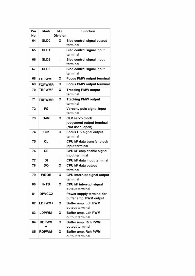
64 SLD0 O Sled control signal output terminal
65 SLD1 I Sled control signal input terminal
66 SLD2 I Sled control signal input terminal
67 SLD3 I Sled control signal input terminal
68 FOPWMF O Focus PMW output terminal69 FOPWMR O Focus PMW output terminal70 TRPWMF O Tracking PMW output
terminal71 TRPWMR O Ttacking PMW output
terminal72 FG I Verocity puls signal input
terminal73 D4M O CLV servo clock
judgement output terminal (Not used, open)
74 FOK O Focus OK signal output terminal
75 CL I CPU I/F data transfer clock input terminal
76 CE I CPU I/F chip enable signal input terminal
77 DI I CPU I/F data input terminal78 DO O CPU I/F data output
terminal79 WRQB O CPU interrupt signal output
terminal80 INTB O CPU I/F interrupt signal
output terminal81 DPVCC2 — Power supply terminal for
buffer amp. PWM output82 LDPWM+ O Buffer amp. Lch PWM
output terminal83 LDPWM- O Buffer amp. Lch PWM
output terminal84 RDPWM
+O Buffer amp. Rch PWM
output terminal85 RDPWM- O Buffer amp. Rch PWM
output terminal

Pin No.
Mark I/O Division
Function
86 DPVSS — GND terminal for buffer amp. PWM output
87 VDD I Power supply input terminal
88 XIN I 16.9344MHz oscillate input terminal
89 XOUT O 16.9344MHz oscillate output terminal
90 VSS — GND terminal91 VCC2 I Power supply input
terminal92 DDOUT O Digital audio output
terminal (Not used, open)93-105
NC — Not used, open
106 VSS — Connected to GND107 VCC2 I Power supply input
terminal108 TEST2 I Test terminal (Connected
to power supply)109-114
NC — Not used, open
115 SMON3 I Monitor signal output terminal (Not used, open)
116 SMON2 O Monitor signal output terminal
117 SMON1 O Monitor signal output terminal
118 SMON0 — Monitor signal output terminal (Not used, open)
119 NC — Not used, open120 VSS — Connected to GND
14.3. IC201 (MN101C32GAG2): SYSTEM CONTROL

Pin No.
Mark I/O Division
Function
1 VREF- — Connected to GND2 REM_KEY I Remote control key input
terminal3 KEYIN I Unit key input terminal4 BATT I Battery voltage detection
input terminal5 (AN3) — Connected to GND6 (AN4) — Connected to GND7 (AN5) — Connected to GND8 OUTC — Not used, open9 VPP I Power supply input
terminal10 VREF+ I Power supply input
terminal11 VDD I Power supply input
terminal12 OSC2 O System clock output
terminal (F=6MHz)13 OSC1 I System clock input
terminal (F=6MHz)14 VSS — Connected to GND15 XI — Sub clock input terminal
(Not used, connected to GND)
16 XO — Sub clock output terminal (Not used, open)
17 MMOD — Memory mode switching input terminal (Not used, connected to GND)
18 REM_DATA O LCD driver data output terminal
19 LINK_IN I LINK serial data input terminal
20 — — Not used, open21 — — Not used, open22 5V_CONT — Not used, open23 SC_DET — Not used, open24 BUZZER O Beep signal output terminal25 RST I Reset signal input terminal26 SETR O EQ frequency gain
switching output terminal27 — — Not used, open

Pin No.
Mark I/O Division
Function
28 BWCT O EQ frequency gain switching output terminal
29 CHARGE O Recharge control output terminal
30 LD_PWM O Laser power controlling PWM output terminal
31 DCIN_ WAKEUP
I Charger starting detection signal input terminal
32 INTB I IC101 interrupt signal input terminal
33 WRQB I IC101 interrupt signal input terminal
34 OPEN_SW I Lid open/ close detection input terminal (H: Open/ L: Close)
35 — — Not used, open36 SSDW O IC101 I/F write data output
terminal37 SSDR I IC101 I/F read data input
terminal38 SSCLK O IC101 I/F clock output
terminal39 SELAD O IC101 I/F address select
output terminal40 RESET B O IC101 I/F reset output
terminal41 ZDTCL I IC101 I/F monitor signal
input terminal42 ZDTCR I IC101 I/F monitor signal
input terminal43 — — Not used, open44 BATT_SW O Battery control signal
output terminal45 MUTE_C O Noise measure low pass
filter control terminal46 — — Not used, open47 — — Not used, open48 PLAY_KEY I PLAY key starting input
terminal49 REM_WUP I Remote control key wake
up input terminal

Pin No.
Mark I/O Division
Function
50 ELON O EL display control output terminal (L: Start)
51 — — Not used, open52 FOK I Focus OK signal input
terminal53 DRV_STBY O Driver IC standby output
terminal54 SP_STBY O Driver IC circuit spindle
standby output terminal55 MUTE_P — Not used, open56 — — Not used, open57 EEP_DATA_I I EEP ROM data input
terminal58EEP_DATA_O O EEP ROM data output
terminal59 EEP_CLK O EEP ROM clock output
terminal60 EEP_CS O EEP ROM chip select
output terminal61 LSI_
STATUS— Not used, open
62 ST_READ — Not used, open63 GHSW O Pit/ Group gain switching
signal output terminal64 RFCONT O RF amp. power supply
control output terminal (L: ON)
65 P.CONT O Power supply control output terminal (H: Power OFF/ L: Power ON)
66 NC — Not used, open67 MODEL
1I Model switching input
terminal (1)68 NC — Not used, open69 DOCTOR I Process inspection mode
input terminal (Connected to power supply through resistor)
70 HOLD I HOLD switch input terminal71 MUTEA O Analog mute A output
terminal

Pin No.
Mark I/O Division
Function
72 3DSW O Head phone surround mode change switch output terminal
73 MUTE_ MODE
I Mute mode dicision input terminal (Connect to GND)
74LED_CNT6_LP4_RO RED LED (PLAY1) control output terminal
75LED_CNT5_LP2_GO GREEN LED (PLAY2) control output terminal
76LED_CNT4_G O GREEN LED (R_SKIP) control output terminal
77LED_CNT3_G O GREEN LED (VOL-) control output terminal
78LED_CNT2_G O GREEN LED (F_SKIP) control output terminal
78LED_CNT1_G O GREEN LED (VOL+) control output terminal
80 ADJ_OK — Not used, open
14.4. IC301 (C0GBZ000009): FOCUS/TRACKING COIL/TRAVERSE MOTOR DRIVE/SPINDLE MOTOR DRIVE/ROTARY DETECTOR
Pin No.
Mark I/O Division
Function
1 IN1R I H bridge (1) logic reverse input terminal
2 CP1 O Charge pump gain puls output terminal
3 CPC1 I Charge pump gain input terminal
4 CP2 O Charge pump gain puls output terminal
5 CPC2 I Charge pump gain input terminal
6 VG O Charge pump gain output trminal (Connected to GND through capacitor)
7 VCC I Small signal block power supply input terminal
8 CLK I Reference clock signal input terminal

Pin No.
Mark I/O Division
Function
9 MODE I PWM frequency switching input terminal
10 VS I 3-phase sled drive power supply input terminal
11 BRK I Spindle motor block brake input terminal
12 PGND4 — GND terminal13 SUCO O Sled driver block position
detection comparator output terminal
14 SUO O 3-phase sled (U) output terminal
15 SVO O 3-phase sled (V) output terminal
16 SVCO O Sled driver block position detection comparator output terminal
17 SWCO O Sled driver block position detection comparator output terminal
18 SWO O 3-phase sled (W) output terminal
19 SCOM I Sled driver block position detection comparator input terminal
20 WOUT O 3-phase spindle (W) output terminal
21 VOUT O 3-phase spindle (V) output terminal
22 COM I Spindle motor COM point connect input terminal
23 UOUT O 3-phase spindle (U) output terminal
24 FG O FG pulse output terminal25 RF — Output current detection
input terminal (Connected to GND)
26 VS I Spindle motor drive power supply input terminal
27 S3 I 3-phase sled block logic input terminal
28 S2 I 3-phase sled block logic input terminal

Pin No.
Mark I/O Division
Function
29 S1 I 3-phase sled block logic input terminal
30 PWM I PWM signal input terminal (H: Output TR ON)
31 GND — GND terminal32 FIL O Spindle motor position
detection comparator filter output terminal
33 COMIN I Spindle motor position detection comparator filter input terminal
34 VCOIN I VCO control voltage input terminal (Connected to GND through capacitor)
35 VCO — VCO oscillation terminal (Connected to GND through capacitor)
36 RMAX — VCO highest frequency setting terminal (Connected to GND through resistor)
37 IN2R I H bridge (2) logic reverse input terminal
38 IN2F I H bridge (2) logic forward input terminal
39 MUTE I H bridge 1,2 and 3-phase sled mute input terminal
40 VS2 I H bridge (2) motor power supply input terminal
41 OUT2F O H bridge (2) forward output terminal
42 OUT2R O H bridge (2) reverse output terminal
43 PGND1 — GND terminal44 OUT1R O H bridge (1) reverse output
terminal45 OUT1F O H bridge (1) forward output
terminal46 VS1 I H bridge (1) motor power
supply input terminal47 S/S I Spindle motor block start/
stop input terminal (H: Start)

Pin No.
Mark I/O Division
Function
48 IN1F I H bridge (1) logic forward input terminal
15. Caution in Use of Rechargeable Battery Ass'y- Take Rechargeable Battery Ass’y out of Battery Carrying Case and
use it.- Be sure to carry Rechargeable Battery Carrying Case. If not, it may
either heat or ignite by shorting with a metal. (as shown in Fig. 10 )Fig. 10
16. Supply of Rechargeable Battery Ass'y as Replacement PartsPlease take note of the following points relating to Battery Carrying Case to be used for protection of Rechargeable Battery Ass’y from shorting. Replacement Parts:- Rechargeable Battery Ass’y (RFKFFAZ01EM1) supplied will be
provided with Battery Carrying Case (RFA0475-Q).- No replacement parts will be supplied for Rechargeable Battery
Ass’y without Battery Carrying Case.- Replacement parts will be supplied for Battery Carrying Case
(RFA0475-Q) without Rechargeable Battery Ass’y.- To your customers, delivery Rechargeable Battery Ass’y together
with Battery Carrying Case to prevent shorting accidents that may occur when Rechargeable Battery Ass’y is carried about Battery Carrying Case. (as shown in Fig. 11 )
Fig. 11

17. Replacement Parts ListNotes:*Important safety notice: / Components identified by mark have special characteristics important for safety.*Furthermore, special parts which have purposes of fire-retardant (resistors), high-quality sound (capacitors), low-noise (resistors), etc. are used.*When replacing any of components, be sure to use only manufacture’s specified parts shown in the parts list.*Warning: This product uses a laser diode. Refer to caution statements.*Capacity values are in microfarads (uF) unless specified otherwise, P=Pico-farads (pF) F=Farads (F)*Resistance values are in ohms, unless specified otherwise, 1K=1,000 (OHM), 1M=1,000K (OHM)*The marking <RTL> indicates that the Retention Time is limited for this item. After the discontinuation of this assembly in production, it will no longer be available.*"<IA>" mark in Remarks indicates languages of instruction manual.[<IA>: English/ Chinese]*All parts are supplied by MESA.

Ref. No. Part No. Part Name & Description Pcs Remarks
1 RDG0477 INTERMEDIATE GEAR 12 RHD14078 SCREW 13 RHW11011 WASHER 14 RMC0483 HOLDER SPRING 15 RXK0354-1 TRAVERSE UNIT 15-1 BRL1A1CWB TRAVERSE MOTOR 15-2 RHD14074 SCREW 15-3 RJC99038-2 RECHARGE.BATT.TERMINAL(-) 15-4 XQN14+B2FC SCREW 16 RAF2000A-4M OPTICAL PICK-UP 1 7 RXJ0025-1 DRIVE SHAFT 18 RHD14067 SCREW 59 RJC99039-1 RECHARGE.BATT.TERMINAL(+) 110 RJR0195-2 BATTERY SHAFT 112 RHQ0083-S SCREW 613 RXQ0982 LINK UNIT(R) 114 RXQ0984 LINK UNIT(L) 114-1 RGU2040-S1 EJECT KNOB 115 RYF0652-S DISC COVER 116 RYK1256-S INTERMEDIATE CABINET 117 RYK1257A-S CABINET ASS’Y 117-1 RGV0296-S HOLD KNOB 118 RHD14076-S SCREW 619 RKK0156-S BATTERY COVER 120 RMQ1205 SPACER 1
A1 K3ZZ00200038 EXTERNAL BATTERY CASE 1A2 L0BAB0000174 STEREO EARPHONES 1A3 L0EAAB000011 SPEAKER BATTERY CHARGER 1A4 N0JCBD000001 AC ADAPTOR 1 A5 N2QCBD000020 WIRED REMOTE CONTROLLER 1A5-1 RFKY0010 REMOCON PANLE ASS’Y 1A5-2 RFKY0004 REMOCON CLIP ASS’Y 1A6 RFKFFAZ01EM1 RECHARGE. BATTERY ASS’Y 1A6-1 RFA0475-Q RECHARGE. BATT.CASE 1A7 RFC0074-H SOFT CASE 1A8 RQT6640-K OPERATING INSTRUCTION 1 <IA>
C1 ECUE1E332KBQ 25V 3300P 1 F1G1E332A059C2 F5A421050001 4V 1U 1C4 F1G0J224A004 6.3V 0.22U 1C5 F3E0G226A002 4V 22U 1C7 F5A422240001 4V 0.22U 1C9 F1G1C103A044 16V 0.01U 1C10 F1G1H100A420 50V 10P 1C13 F1G1H2R0A424 50V 2P 1C20 F1J0J4750010 6.3V 4.7U 1C24 F1G1C103A044 16V 0.01U 1C28 F3E0G226A002 4V 22U 1C101,02 F1G1C103A044 16V 0.01U 2C103 ECJ1VB0J105K 6.3V 1U 1C105-07 ECUENA104KBQ 10V 0.1U 3 F1G1A104A014C108 ECUE1H102KBQ 50V 1000P 1 F1G1H102A457

C108 ECUE1H102KBQ 50V 1000P 1 F1G1H102A457

Ref. No. Part No. Part Name & Description Pcs RemarksC113 ECUENA104KBQ 10V 0.1U 1 F1G1A104A014C115 ECUENA104KBQ 10V 0.1U 1 F1G1A104A014C116 ECJ0EB1C822K 16V 8200P 1C117 ECUE1H102KBQ 50V 1000P 1 F1G1H102A457C130 ECJ1VB0J105K 6.3V 1U 1C131,32 F1G1E472A059 25V 4700P 2C133 F3E0G106A001 4V 10U 1C201 F1G1C103A044 16V 0.01U 1C202 ECJ0EB1H101K 50V 100P 1C203 F1J0J4750010 6.3V 4.7U 1C204 ECUENA104KBQ 10V 0.1U 1 F1G1A104A014C206 ECJ0EB1H101K 50V 100P 1C210 F1G1C103A044 16V 0.01U 1C211 ECUVNJ474KBV 6.3V 0.47U 1 F1H0J474A002C212 F1G1C103A044 16V 0.01U 1C214 F5A422240001 4V 0.22U 1C220 ECJ0EB1H101K 50V 100P 1C221 ECUE1H102KBQ 50V 1000P 1 F1G1H102A457C304 ECUE1E332KBQ 25V 3300P 1 F1G1E332A059C305 ECJ2YB0J225K 6.3V 2.2U 1C306 F1G1H222A416 50V 2200P 1C307 F1J0J4750010 6.3V 4.7U 1C310 F5A422240001 4V 0.22U 1C311 F1G0J224A004 6.3V 0.22U 1C330 ECJ1VB0J105K 6.3V 1U 1C401 F3Z0G107A003 4V 100U 1C402 F3E0G226A002 4V 22U 1C403 F1G1C103A044 16V 0.01U 1C404 F3G0G2270001 4V 220U 1C405 F3Z0J106A001 6.3V 10U 1C406,07 F1J0J4750010 6.3V 4.7U 2C410 ECUENA104KBQ 10V 0.1U 1 F1G1A104A014C411 F1G1C103A044 16V 0.01U 1C412 ECUENA104KBQ 10V 0.1U 1 F1G1A104A014C413 F3F1A226A008 10V 22U 1C415 F1G1C103A044 16V 0.01U 1C421 F1G1H330A422 50V 33P 1C501 F3E0G226A002 4V 22U 1C502 ECUENA104KBQ 10V 0.1U 1 F1G1A104A014C503 ECUVNJ334KBV 6.3V 0.33U 1 F1H0J334A002C504 F5A421050001 4V 1U 1C505 F3E0G106A001 4V 10U 1C507,08 F3G0E2270001 2.5V 220U 2C509 F1J0J4750010 6.3V 4.7U 1C511 F5A421020001 4V 1000P 1C515 F5A422240001 4V 0.22U 1C523 F5A421040002 4V 0.1U 1C551-53 F1G1C103A044 16V 0.01U 3C602,03 F1G1E472A059 25V 4700P 2C604,05 F5A421050001 4V 1U 2C608,09 F1G1H151A016 50V 150P 2C610 F3E0G106A001 4V 10U 1C611-13 F1G1H680A410 50V 68P 3C614 F3E0G106A001 4V 10U 1

Ref. No. Part No. Part Name & Description Pcs RemarksC615 ECUENA104KBQ 10V 0.1U 1 F1G1A104A014C616 F1G1H680A410 50V 68P 1C621,22 F1G1H271A401 50V 270P 2C801 F5A421050001 4V 1U 1C803-06 F1J0J4750010 6.3V 4.7U 4C807,08 F3F1A226A008 10V 22U 2
CP1 RJS2A7121T CONNECTOR(21P) 1 K1MN21B00028CP201 K1MN13B00065 CONNECTOR(13P) 1CP301,02 RJS2A7104T CONNECTOR(4P) 2 K1MN04A00014CP801 K4BZ07E00001 CONNECTOR(7P) 1
CX110,11 ECUE1E472KBQ 25V 4700P 2 F1G1E4720004CX222 ECUENA104KBQ 10V 0.1U 1 F1G1A104A014CX415 F1G1E472A059 25V 4700P 1CX451 F1J0J4750010 6.3V 4.7U 1CX811,12 ECUE1C153KBQ 16V 0.015U 2 F1G1C153A044
D402,03 B0JCJB000001 DIODE 2D406 MA2YD2100L DIODE 1
IC1 C1BB00000728 IC 1IC101 C1BB00000729 IC 1IC201 MN101C32GAG2 IC 1IC202 C3EBDG000039 IC 1IC203 C0EBC0000032 IC 1IC301 C0GBZ0000009 IC 1IC401 XC6367A151MR IC 1 C0DBAFZ00012IC402 C0DBAFZ00021 IC 1IC403 C0DBAGZ00016 IC 1IC404 B1KBB0000006 IC 1IC501 C1BB00000720 IC 1IC601 C1BB00000730 IC 1IC602 NJU7015RTE1 IC 1 C0ABHA000012IC801,02 NJM2135RTE1 IC 2 C0ZZZ0000014
JK501 RJJ36TA02-C JACK,HEADPHONE 1 K2HC106E0003
L201 G1C100Z00011 COIL 1L401 G1C100Z00011 COIL 1L402 G1A330D00007 COIL 1L403 RLQP100MT-W COIL 1 G1C100M00016L405 G1A150D00002 COIL 1L406 ELJEA470KF COIL 1L501,02 RLBV601V-W COIL 2 J0JCC0000059
P1 RPK1852 PACKING CASE 1P2 RPQ1442 PAD 1P3 RPF0257-1 PROTECTION BAG 1P4 RPQ1443 PAD 1
PCB1 REP3453A-M MAIN P.C.B. ASS’Y 1 (RTL)
Q1 B1ADMB000003 TRANSISTOR 1

Ref. No. Part No. Part Name & Description Pcs RemarksQ5 B1CHMC000001 TRANSISTOR 1Q201 2SD1819ASTX TRANSISTOR 1 2SD1819ASLQ202 B1ADMB000003 TRANSISTOR 1Q203-05 B1GFCFJN0013 TRANSISTOR 3Q402,03 B1CHMC000001 TRANSISTOR 2Q404,05 B1DFAC000003 TRANSISTOR 2Q406,07 2SB1218ASTX TRANSISTOR 2 2SB1218ASLQ408 B1HFCFA00005 TRANSISTOR 1Q410 B1DFAC000003 TRANSISTOR 1Q411 B1MBADA00001 TRANSISTOR 1Q412 B1DFAC000003 TRANSISTOR 1Q551 MCH6602-TL TRANSISTOR 1 B1CFHD000004
R1 D1H411320001 11K 1R2 ERJ2GEJ471X 1/4W 470 1 ERJ2RMJ471XR3 ERJ2GEJ391X 1/4W 390 1 ERJ2RMJ391XR4 ERJ2GEJ104 1/4W 100K 1R5 ERJ2GEJ1R0X 1/4W 1 1 ERJ2RMJ1R0XR7 ERJ2GEJ223X 1/4W 22K 1 ERJ2RMJ223XR8 ERJ2GEJ474X 1/4W 470K 1 ERJ2RMJ474XR9 ERJ2GEJ823X 1/4W 82K 1 ERJ2RMJ823XR101 ERJ2GEJ472X 1/4W 4.7K 1 ERJ2RMJ472XR102 ERJ2GEJ222X 1/4W 2.2K 1 ERJ2RMJ222XR103 ERJ2GEJ682X 1/4W 6.8K 1 ERJ2RMJ682XR104 ERJ2GEJ473X 1/4W 47K 1 ERJ2RMJ473XR106 ERJ2GEJ105 1/4W 1M 1 D0GA105JA001R107 ERJ2GE0R00X 1/4W 0 1 D0YAR0000003R108 ERJ2GEJ682X 1/4W 6.8K 1 ERJ2RMJ682XR109 ERJ2GEJ332X 1/4W 3.3K 1 ERJ2RMJ332XR112 ERJ2GEJ224 1/4W 220K 1R113 ERJ2GEJ103 1/4W 10K 1R115 ERJ2GEJ393X 1/4W 39K 1 ERJ2RMJ393XR116 ERJ2GEJ103 1/4W 10K 1R117 ERJ2GEJ101 1/4W 100 1R120 ERJ2GEJ473X 1/4W 47K 1 ERJ2RMJ473XR131 ERJ2GEJ101 1/4W 100 1R201 ERJ2GEJ103 1/4W 10K 1R202 ERJ2GEJ473X 1/4W 47K 1 ERJ2RMJ473XR203 ERJ2GEJ221 1/4W 220 1R204 ERJ2GEJ332X 1/4W 3.3K 1 ERJ2RMJ332XR205 ERJ2GEJ682X 1/4W 6.8K 1 ERJ2RMJ682XR206 ERJ2GEJ223X 1/4W 22K 1 ERJ2RMJ223XR207 ERJ2GEJ471X 1/4W 470 1 ERJ2RMJ471XR208 D1H422420001 220K 1R209 D1H410320002 10K 1R215 ERJ2GEJ223X 1/4W 22K 1 ERJ2RMJ223XR216 D1H422420001 220K 1R218 ERJ2RHD273X 1/4W 27K 1R219 ERJ2GEJ104 1/4W 100K 1R221 D1H410320002 10K 1R231 ERJ2GEJ101 1/4W 100 1R233,34 D1H410120001 100 2R301 ERJ2GEJ103 1/4W 10K 1R302 ERJ2GEJ1R0X 1/4W 1 1 ERJ2RMJ1R0X

Ref. No. Part No. Part Name & Description Pcs RemarksR303 ERJ2GEJ682X 1/4W 6.8K 1 ERJ2RMJ682XR305 ERJ2GEJ393X 1/4W 39K 1 ERJ2RMJ393XR401 ERJ2GEJ225X 1/4W 2.2M 1 ERJ2RMJ225XR402 D1H84744A024 470K 1R403 D1H447420001 470K 1R404 ERJ2GEJ274X 1/4W 270K 1 D0GA274JA001R405 ERJ2GEJ105 1/4W 1M 1 D0GA105JA001R406 D1H84744A024 470K 1R407 ERJ2GEJ103 1/4W 10K 1R408 ERJ3GEYJ101 1/16W 100 1 D0GB101JA002R410 ERJ6GEYJ4R7V 1/10W 4.7 1R412 ERJ2RKD684X 1/4W 680K 1R413 ERJ2RKD474X 1/4W 470K 1R421 ERJ2RKD684X 1/4W 680K 1R422 ERJ2GEJ104 1/4W 100K 1R423 ERJ2GEJ823X 1/4W 82K 1 ERJ2RMJ823XR501 D1H439220001 3.9K 1R504 D1H410320002 10K 1R506 EXB24V225JX 1/4W 2.2M 1R507 D1H410020002 10 1R509 ERJ2GEJ221 1/4W 220 1R551 D1H447420001 470K 1R553 ERJ2GEJ474X 1/4W 470K 1 ERJ2RMJ474XR602 ERJ2GEJ183 1/4W 18K 1R603 ERJ2GEJ682X 1/4W 6.8K 1 ERJ2RMJ682XR604 ERJ2GEJ104 1/4W 100K 1R605 D1H84734A024 47K 1R606 ERJ2GEJ470 1/4W 47 1R607 D1H427320001 27K 1R608 ERJ2GEJ273X 1/4W 27K 1 ERJ2RMJ273XR609 D1H422320002 22K 1R610 D1H84734A024 47K 1R611 ERJ2GEJ273X 1/4W 27K 1 ERJ2RMJ273XR621 D1H84734A024 47K 1R801,02 ERJ2GEJ152 1/4W 1.5K 2R803,04 ERJ2GEJ183 1/4W 18K 2R805,06 ERJ2GEJ224 1/4W 220K 2R810,11 ERJ2GEJ2R2X 1/4W 2.2 2 ERJ2RMJ2R2XR812,13 ERJ2GEJ150 1/4W 15 2
RX210 ERJ2GEJ104 1/4W 100K 1RX808,09 ERJ2GEJ821X 1/4W 820 2 ERJ2RMJ821X
S207 RSH1A039-A SW,OPEN/CLOSE DET. 1 K0L1BA000037S208 RSS2A010-1A SW,HOLD 1 K0D112B00071
X101 H2D169500017 OSCILLATOR 1X201 H2D400400010 OSCILLATOR 1
Z401 RJH9212-1 CONNECTOR TERMINAL 1 K4BC02E00007
18. Cabinet Parts Location

19. Packaging

20. Schematic Diagram for Printing with A4 SizeH0211TN/HH