Embed Size (px)
DESCRIPTION
CoinCraft+A1
Citation preview

Copyright © 2013 Bitmine AG – All rights reserved 1
Bitmine CoinCraft A1 Bitcoin mining dedicated ASIC Product outline: The CoinCraft A1 is a custom developed, highly optimized hardware implementation of the Bitcoin block hashing algorithm. The A1 uses an industry standard SPI interface and supports daisy chain configurations up to 253 units. The A1 can cover a wide range of applications, from ultra low power to high end, high performances. Specifications:
• Developed on 28nm HPP (High Performance Process) from Global Foundries.
• Custom IC package with power bars for low voltage, high current feeding.
• Configurable in daisy chain mode for distributed work with up to 253 ASICs.
• Standard SPI interface.
• 32 highly optimized hashing engines based on custom ASIC cells.
• Hashing power of 20 GH/s in low power, 25 GH/s in nominal and up to 40 GH/s in Turbo mode.
• Power usage of 0.35 W/GH in low power, 0.6 W/GH in nominal and 1 W/GH in Turbo
mode.
• Supply voltage of 0.65V in low power, 0.765 V in nominal and 0.85 V in Turbo mode.
• Product available starting from the second week of December 2013.

Copyright © 2013 Bitmine AG – All rights reserved 2
1. Protocol specification
1.1 General protocol specifications.
The CoinCraft A1 uses two SPI ports, one used in slave mode as an input from the uC or the previous A1 in the chain (pins SDO_R, SDI_R, SCK_R, CS_R) and one in master mode to the next A1 in the chain (pins SDO_L, SDI_L, SCK_L, CS_L), if any. The SPI bus can operate at any clock speed up to 20 MHz. The clock is supplied by the uC through the IN_SCLK pin and passed to the next A1 in the chain through OUT_SCLK. A 16 bit SPI bus is used all the time, every frame is made of 16 bit command/address field followed by 16 bit based data, if any data is to be followed by the command. The CS pins are used to qualify one frame from the master. There is no need for CS on the response frames because the uC has knowledge of the length that the frame should have. The first 8 bit in the frame is the command field which is listed on Table 1 below, the second 8 bit is the addressing. If the address is set to 00, the command is meant to be broadcast among all the A1 in the chain. At reset, an automatic configuration mode enumerates and assigns addresses to all the chips in the chain. The first one will get address 0x01, the second one 0x02 and so on up to the last chip in the chain or to the maximum possible address of 0xFF. Most command will loop back to uC through the chain to indicate to the uC that the job was executed. Some command such as BIST_ON or AUTO_ADDRESSING command will modify the 0x00 address field. For example, the AUTO_ADDRESSING command returns the frame with the highest chip address in the chain back to the uC.
Copyright © 2013 Bitmine AG – All rights reserved 3
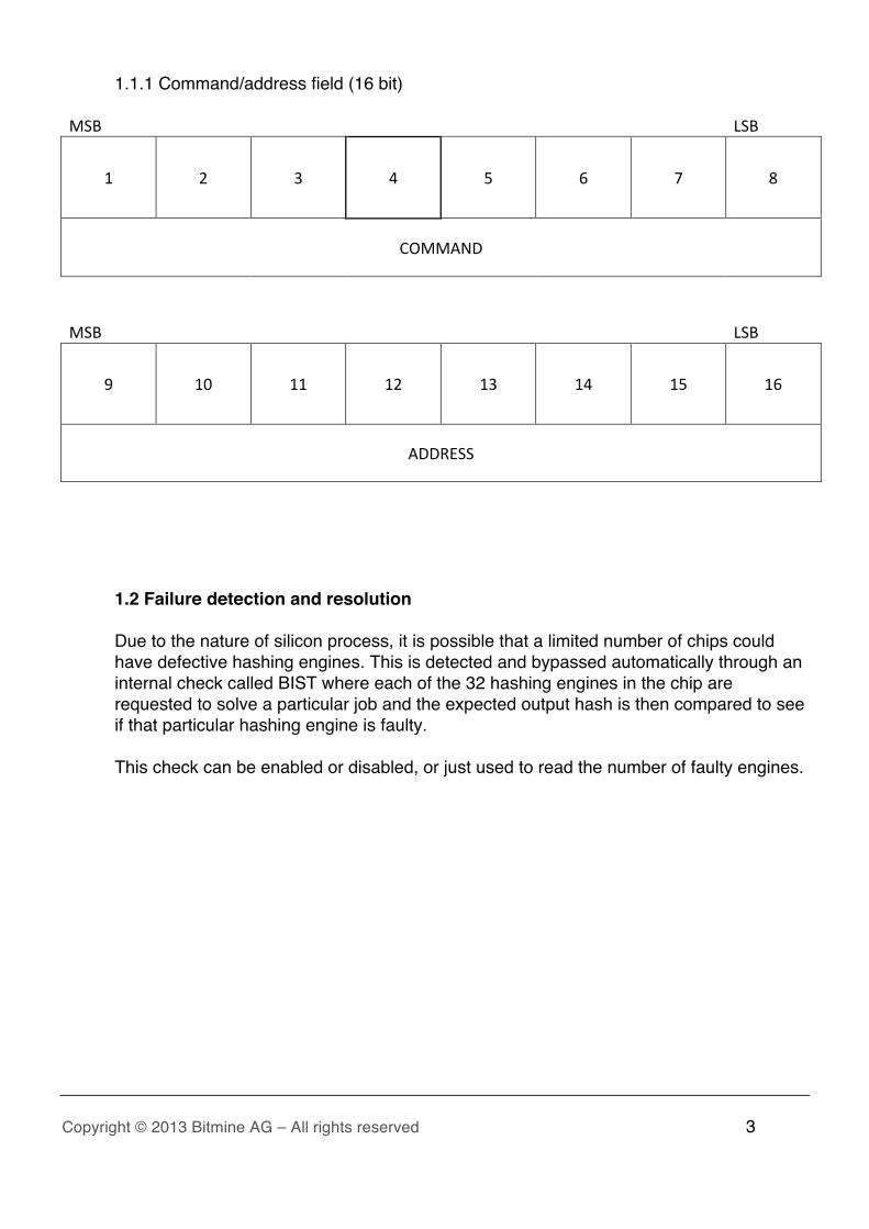
1.1.1 Command/address field (16 bit)
MSB
LSB
1 2 3 4 5 6 7 8
COMMAND
MSB
LSB
9 10 11 12 13 14 15 16
ADDRESS
1.2 Failure detection and resolution Due to the nature of silicon process, it is possible that a limited number of chips could have defective hashing engines. This is detected and bypassed automatically through an internal check called BIST where each of the 32 hashing engines in the chip are requested to solve a particular job and the expected output hash is then compared to see if that particular hashing engine is faulty. This check can be enabled or disabled, or just used to read the number of faulty engines.

Copyright © 2013 Bitmine AG – All rights reserved 4
2. Command reference Command format from uC
Name Broadcast / Individual type
Return format to uC
Description
0x0100 BIST_START / Auto Address
Broadcast 0x0100 0x00NN
Starts BIST check in all chips and auto addressing returns to uC. This returns one 16bit command and one 16 bit data. NN means the last device address in the chain.
0x01NN BIST_START Individual 0x01NN Starts BIST check in the address matching chip and report the same command back to uC.
0x0300 BIST_FIX Broadcast 0x0300
Ask each chip to mux out the bad hashing engines, fix all chips and bypass the hash engines that have been found to be faulty (if any).
0x03NN BIST_FIX Individual 0x03NN Fix one particular chip and bypass the faulty hash engines (if any).
0x0400 RESET Broadcast 0x0400
Reset all chips: reset SPI state machine, the status of the hashing units and the queues based on the configuration currently present in the registers.
0x04NN RESET Individual 0x04NN Reset a particular chip: reset SPI state machine, the status of the hashing units and the queues based on the configuration currently present in the registers.

Copyright © 2013 Bitmine AG – All rights reserved 5
Command format from uC
Name Broadcast / Individual type
Return format to uC
Description
0x17NN WRITE_JOB
Individual 0x17NN
Send a new job to a specific chip, pushing it in the input queue and assigning it the JOB_ID 1.
0x27NN WRITE_JOB
Individual 0x27NN Send a new job to a specific chip, pushing it in the input queue and assigning it the JOB_ID 2.
0x37NN WRITE_JOB
Individual 0x37NN Send a new job to a specific chip, pushing it in the input queue and assigning it the JOB_ID 3.
0x47NN WRITE_JOB
Individual 0x47NN Send a new job to a specific chip, pushing it in the input queue and assigning it the JOB_ID 4.
0x0800 READ_RESULT Broadcast
0x0800 if no match 0xY8NNDATA if match, JOB_ID is Y.
Read result frame from all chips, 1st chip in the chain that has a result in the output queue will swap command bit and return it as 0xY8NN, followed by the matched data. The Y identifies the JOB_ID of the returned nonce. The uC should store the data, then send out another 0x0800 to see if any other chip has results pending to be read, and so on till 0x0800 is read back, which means no more results are available in the chain. The uC can associate the returned nonce to a particular work by checking the JOB_ID field.
0x08NN READ_RESULT Individual 0x08NN if no match 0xY8NNDATA if match, JOB_ID is Y.
Read result frame from a specific chip, if it has a result in the output queue it will swap command bit and return it as 0xY8NN, followed by the matched data. The Y identifies the JOB_ID of the
Copyright © 2013 Bitmine AG – All rights reserved 6
returned nonce. The uC should store the data, then send out another 0x0800 to see if any other chip has results pending to be read, and so on till 0x0800 is read back, which means no more results are available in the output queue. The uC can associate the returned nonce to a particular work by checking the JOB_ID field.
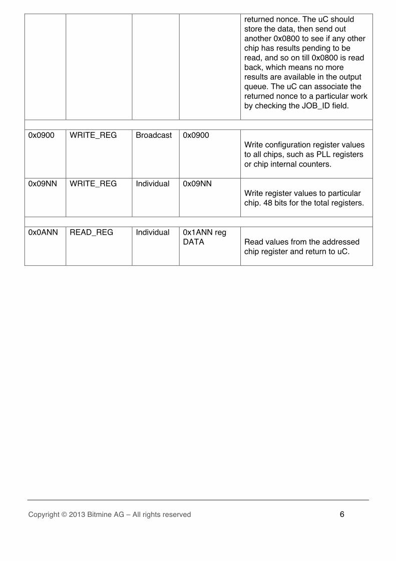
0x0900 WRITE_REG Broadcast 0x0900
Write configuration register values to all chips, such as PLL registers or chip internal counters.
0x09NN WRITE_REG Individual 0x09NN Write register values to particular chip. 48 bits for the total registers.
0x0ANN READ_REG Individual 0x1ANN reg
DATA Read values from the addressed chip register and return to uC.

Copyright © 2013 Bitmine AG – All rights reserved 7
Register Pins Description register[46:45] pll_postdiv[1:0] PLL post divider register[44:40] pll_prediv[4:0] PLL pre divider register[39:31] pll_fbdiv[7:0], pll_fbdiv[8] PLL fb divider register[30] pll_incz register[29] pll_lock_en register[28] pll_clock_out_enable register[27] pll_powerdown register[26] pll_test_enable register[25:24] pll_test_select register[23:8] reserved Reserved for future use register[7:0] bct_good_cnt[7:0]
Read only field, indicates how many hashing engines have passed the BIST self test. Maximum 32, minimum 1.
3. Registers reference The 48 bits register inside each chip is described as below. Through command 0x0900 WRITE_REG, the payload data is fed in the format of MSByte and MSBit first.

Copyright © 2013 Bitmine AG – All rights reserved 8
4. Firmware implementation reference guide All command follows the standard SPI format with CS to indicate the start and end of packet. There is a MPU and a chip chain which is driven by MPU clocks to flow through command/address/data packets. The SPI bus clock can run as high as 20MHz. Any command and data is 16 bits based and MPU will receive a response for each command execution. All payload data, such as register value, job data or hashout result are MSB first. The workflow follows the sequence, and this is what firmware should do. 1. System Initialization Power up and Hardware reset MPU broadcast the reset packet (0x0400) to all chips Command packet format: 0x0400 with CS then keep the SCLK going to push forward After the whole chain, MCU will receive a response: 0x0400 Action: All chips in the chain, when receiving this command, will all clear out any ongoing activities and reassert the reset values in the registers. 2. WRITE_REG, overwrite the PLL and any additional configuration registers if needed MPU broadcasts the wanted configuration register values to all chips if the default values aren’t already fine. REG_WRITE command format: 0x0900 0xXXXX 0xXXXX 0xXXXX (48 bit data payload) After the whole chain, MCU will receive a response: 0x0900 0xXXXX 0xXXXX 0xXXXX Action: The default values of register in the recipient chip will be overwritten by this command, such as PLL divider, reset_ and so on. This command consists of four 16 bit values. The first one is the WRITE_REG command. Next three are the assigned register values (0xXXXX indicates 16 bits value in hexadecimal format). 3. BIST_START/Auto addressing MPU broadcasts the BIST_START command to all chips, starts BIST and auto addressing

Copyright © 2013 Bitmine AG – All rights reserved 9
Command packet format: 0x0100 Response: 0x0100 0x00NN (NN comes back with auto addressing’s total number of chips in the chain). Action: This message starts the BIST mode for all the chips in the chain. In addition, system auto addressing completes (all chips will be assigned the address automatically). When the BIST runs for a certain period (66 internal clock cycles), the BIST will be finished and will store the number of good hashing units into each chip’s register but won’t disable the hashing engines found to be faulty. 4. BIST_FIX to bypass all bad hash engines inside a chip MPU broadcast the BIST_FIX to all chips Command packet format: 0x0300 Response: 0x0300 Action: This fixes all bad hashes inside chips and bypasses the faulty hash engines. 5. Read the register from specific chip such as good Hash count inside each chip MPU sends the READ_REG to specific chips in the chain. Command packet format: 0x0aNN (NN indicates the specific chip’s address) Response: 0x1ANN 0xXXXX 0xXXXX 0xXXXX Action: The good hashing engines number is stored in the register and can be read from the chip. 0x1ANN indicates that this command is acknowledged by the specific chip and returns its three 16 bit register values back to MPU (NN is the specific chip address, XX is the register value). 6. Write the job to individual chip and start the computation MPU broadcast the job to all chips Command packet format: 0xY7NN 0xXXXX … 0xXXXX Response: 0xY7NN Action: Jobs are pushed in the input queue of each chip and are identified by the Y parameter which can be anything from 1 to 4, these will be used later by the uC when the results are read to understand which nonce is associated to what job. The job payload has 448 bits data,

Copyright © 2013 Bitmine AG – All rights reserved 10
including 128 bits wData, 256 bits midState, 32 bits TargetDifficulty and 32 bits endNonce (NN is the individual chip address, 0xXXXX indicates 16 bits value). After the job assignment is finished, the hash engine will compute immediately and will push to the output queue all the hash results that are equal or better than the supplied TargetDifficulty parameter. Each chip has two input queue slots, so right after the reset, two distinct jobs should be sent to the chip in order to queue the work. The job ID doesn’t have to be sequential, just make sure that it doesn’t overlap with a job already queued or being processed. 7. Read the matched result from all chips MPU broadcast the command (0x0800) to all the chips in the chain. Command packet format: 0x0800, Response: 0x0800 if there are no chips get the matched hash value. 0xY8NN 0xXXXX … 0xXXXX if NN chip gets the matched hash result. Action: 0xY8NN is the acknowledge command returned back to MPU, followed by 32 bits Nonceout (NN is the response chip address, 0xXXXX indicates 16 bits value). The original job id of the resulting nonce is given back with the Y parameter. Depending on the set target difficulty, more than one match is possible within the same job, as such the searching will not stop when a match is found but will continue till the 32 bit nonce counter overflows. Each chip has five output queues so each chip has potentially enough room to hold results for any match given by the queues jobs. 8. Read the matched result and keep feeding new jobs Knowing the speed at which hashes are tried, the uC should keep trace of the elapsed time since the last job was sent and make sure that another new job is sent before the second job is pulled from the queue, so that optimal performances are achieved without the chip ever stopping to run. Otherwise, the uC can repeat step 7 until 0xY8NN is received. When 0x0800 is received, it means that the specific chip that answered has run out of jobs and that its input queue should be filled again by getting back to step 6. 9. Watch for new blocks coming from the network In the case that a new network block is broadcast by the Bitcoin network, all currently running jobs should be stopped and discarded to make place for the new ones. This can be achieved by sending the WRITE_REG command with the appropriate fields set to 1 for Input queue and

Copyright © 2013 Bitmine AG – All rights reserved 11
Output queue reset, while keeping the registers for BIST_FIX and BC set to 0 so that these are not reset. After this, send a broadcast RESET command with 0x0400 and return to step 6 for feeding the new jobs to the chain.

Copyright © 2013 Bitmine AG – All rights reserved 12
5. Electrical specifications 5.1 Pinout
TOP VIEW
Name Direction PIN Description VDD_CORE I 1,8,9,10,11,19,
20 Core supply voltage
AVDD I 2,18 IO reference supply voltage 1.8V RESETN I 3 Reset signal, active low. CS_L O 4 SPI master signal chip select SDI_L I 5 SPI master serial data in SDO_L O 6 SPI master serial data out SCK_L O 7 SPI master clock out SCK_R I 12 SPI slave clock in SDI_R I 13 SPI slave serial data in SDO_R O 14 SPI slave serial data out CS_R I 15 SPI chip select signal in

Copyright © 2013 Bitmine AG – All rights reserved 13
CLKMUX I 16 Mux the reference clock and internal PLL clock option: 0 for internal PLL clock as system clock, 1 for reference clock as internal system clock.
CLOCK I 17 Reference clock in, see CLKMUX for function of this pin.
GND Ground 5.2 Electrical specifications Parameter Unit Min. Typ. Max. Core supply voltage (VDD_CORE) V 0.65 0.765 0.85 Core supply current (VDD_CORE) A 12.5 20 30 I/O reference voltage (AVDD) V - 1.8 - I/O reference current (AVDD) A Reference clock for internal PLL (CLKMUX=0)
MHz 12 12 32
System clock (CLKMUX=1)
MHz 600 800 1000
SPI clock (SCK_R and SCK_L) MHz 4 8 20 Junction operating temperature °C 0 - 100 Dissipated power % 25 25 30

Copyright © 2013 Bitmine AG – All rights reserved 14
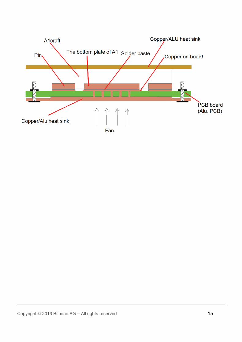
6. Thermal specifications The IC package of the CoinCraft A1 is specifically developed to withstand the high power figures implied in Bitcoin mining specific applications. The QFN package is engineered to transfer most of the generated heat through the ground pad, as illustrated in the typical thermal simulation below:
A system design should account for about 70% of the power being dissipated through the ground pad and about 30% through the top of the package. Appropriate dissipation through ground vias should be engineered in order to transfer the heat from the bottom pad to the bottom layer of the PCB board where an aluminum heat sink should be placed. The illustration below summarizes the typical application of the thermal design of a system featuring the CoinCraft A1.
Copyright © 2013 Bitmine AG – All rights reserved 15

Copyright © 2013 Bitmine AG – All rights reserved 16

Copyright © 2013 Bitmine AG – All rights reserved 17
Revision history Version Date Comments 0.1.A 09.10.13 First public release, work in progress. 0.1.B 17.10.13 Updated IC package to newest version.
Updated PINOUT list. Removed old references to RESP_BIT.
1.0.A 10.11.13 First final release. Updated package drawing. Added electrical specifications. Added thermal specifications.
1.0.B 25.11.13 Revised IC package specification to final (production) version.

Copyright © 2013 Bitmine AG – All rights reserved 18
Copyright © 2013 BITMINE AG BITMINE AG Centro La Monda 2 6528 Camorino Switzerland http://www.bitmine.ch


![3. (M1) 1. a A1 N2 (A1)(A1) A1 N4 - IB relics · P(jar B) 6 = 2 3 §· ¨¸= ©¹ A1 N1 (ii) () 6 PredjarB 8 = 3 4 §· ¨¸= ©¹ A1 N1 [2 marks] (d) recognizing conditional probability](https://img.pdfslide.us/doc/110x75/5ec42be7167ddc3c103f8900/3-m1-1-a-a1-n2-a1a1-a1-n4-ib-relics-pjar-b-6-2-3-a1.jpg)