Embed Size (px)
Citation preview
Coexistence Tips the Market for Wireless System Simulation Chris Aden, MathWorks
Introduction From time to time, marshalling events occur in stable markets placing difficult new requirements on
established system designs. Subsequently, innovative new design tools and processes emerge to address
shortcomings in the legacy design flows for the established systems. In the case of wireless systems, the
emergence of coexistence represents one of these marshalling events. In particular, the connectivity
boom in consumer electronics and the importance of electronic warfare in military environments is
requiring radios to perform in spectrally rich environments. As a consequence, system simulation is
emerging as a necessary complement to static analysis for designing wireless systems.
Wireless Communication System Design Wireless communications systems engineers fill the gap between product managers who define product
requirements and component design engineers who implement designs to meet a set of specifications.
The system engineer’s primary role in the product development process is to select a design
architecture capable of meeting the product requirements and to define a set of specifications for the
component design teams. The difficulties, and subsequent need for design tools, arise when the
product requirements dictate architectures containing coupled subsystems.
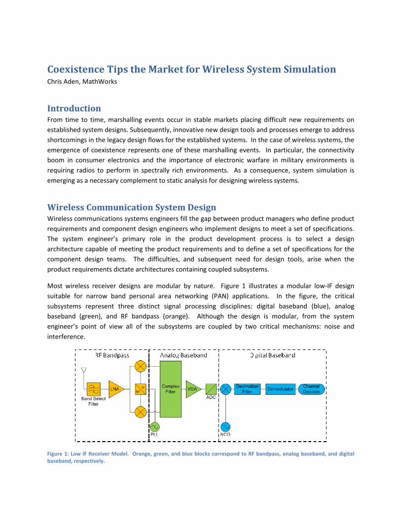
Most wireless receiver designs are modular by nature. Figure 1 illustrates a modular low-IF design
suitable for narrow band personal area networking (PAN) applications. In the figure, the critical
subsystems represent three distinct signal processing disciplines: digital baseband (blue), analog
baseband (green), and RF bandpass (orange). Although the design is modular, from the system
engineer’s point of view all of the subsystems are coupled by two critical mechanisms: noise and
interference.
Figure 1: Low IF Receiver Model. Orange, green, and blue blocks correspond to RF bandpass, analog baseband, and digital
baseband, respectively.
In contemporary receiver designs, the absolute performance bottleneck is determined by the signal to
noise ratio of the waveform incident on the digital receiver. Modules from the analog baseband and RF
domains contribute both noise and interference subsequently raising the required signal-to-noise-plus-
interference ratio (SNIR) of the waveform at the receiver input. After determining a suitable
architecture, the wireless system engineer budgets noise and interference and then assigns
specifications to each subsystem so that the system conforms to his budget.
Figure 2 presents three design structure matrices (DSMs) corresponding to Figure 1 to motivate the
design methodology described in this article. A DSM is a table that captures subsystem dependencies
for a given system architecture. Each subsystem is assigned to a row and column. A dependency
between subsystems is indicated by an entry in the matrix. For example, in DSM 1 all of the subsystems
depend on the design’s frequency plan. By inspection, the ADC carries additional dependencies on the
digital receiver and the analog complex filter. If in a factored DSM all of the dependencies fall below the
main diagonal then a waterfall or sequential design process is used to design the system. When a
factored DSM includes entries above the main diagonal, a spiral design process is often preferred. By
inspection of DSM 1, it can be seen that the low IF receiver in Figure 1 maps to a waterfall design
process.
To reiterate, the primary goal of the system engineer is to determine the radio architecture and a
consistent set of component specifications that enables component design teams (or suppliers) to work
independently. For the remainder of this article, the complete set of specifications for the receiver is
referred to simply as the receiver’s “design rules” [1]. DSM 2 illustrates the goal of the wireless system
engineer, a set of design rules that relaxes all of the dependencies from DSM 1. DSM 3 illustrates an
expanded version of DSM 2 and lists explicitly the design rules that the system engineer provides to the
downstream component design teams. Subsequent sections illustrate how static analysis and system
simulation are used to break the dependencies in DSM 1 to realize the design rules in DSM 3.
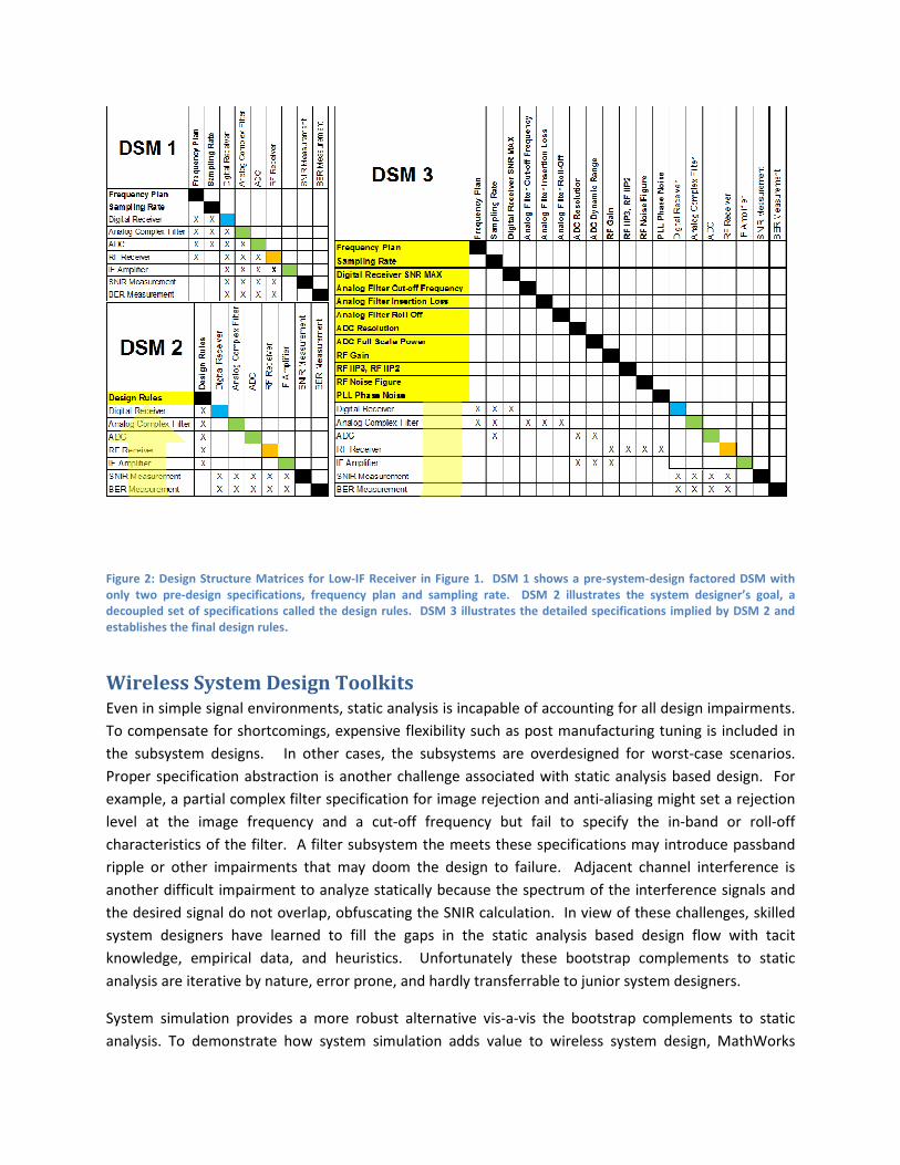
Figure 2: Design Structure Matrices for Low-IF Receiver in Figure 1. DSM 1 shows a pre-system-design factored DSM with
only two pre-design specifications, frequency plan and sampling rate. DSM 2 illustrates the system designer’s goal, a
decoupled set of specifications called the design rules. DSM 3 illustrates the detailed specifications implied by DSM 2 and
establishes the final design rules.
Wireless System Design Toolkits Even in simple signal environments, static analysis is incapable of accounting for all design impairments.
To compensate for shortcomings, expensive flexibility such as post manufacturing tuning is included in
the subsystem designs. In other cases, the subsystems are overdesigned for worst-case scenarios.
Proper specification abstraction is another challenge associated with static analysis based design. For
example, a partial complex filter specification for image rejection and anti-aliasing might set a rejection
level at the image frequency and a cut-off frequency but fail to specify the in-band or roll-off
characteristics of the filter. A filter subsystem the meets these specifications may introduce passband
ripple or other impairments that may doom the design to failure. Adjacent channel interference is
another difficult impairment to analyze statically because the spectrum of the interference signals and
the desired signal do not overlap, obfuscating the SNIR calculation. In view of these challenges, skilled
system designers have learned to fill the gaps in the static analysis based design flow with tacit
knowledge, empirical data, and heuristics. Unfortunately these bootstrap complements to static
analysis are iterative by nature, error prone, and hardly transferrable to junior system designers.
System simulation provides a more robust alternative vis-a-vis the bootstrap complements to static
analysis. To demonstrate how system simulation adds value to wireless system design, MathWorks
Simulink was used to model and simulate the PAN receiver shown in Figure 1. Simulink is unique by
virtue of it’s relevance across all of the critical modeling domains required for wireless system design
and simulation. In particular, MATLAB and Simulink foundation libraries, Control System Toolbox, and
SimPowerSystems support analog baseband design, SimRF supports RF bandpass design, and
Communications System Toolbox and DSP System Toolbox are the industry standard for digital
communication system and DSP design and simulation.
Example Design Intent The existence of the IMT-2000 band for UMTS spanning 2500 MHz to 2690 MHz presents a problem to
devices supporting PAN and local area networks (LAN) utilizing the 2400 MHz ISM band. Since the two
bands are separated by only 16.5 MHz, it is highly unlikely that the receive band filters for the ISM band
system will be selective enough to reject the high power signals originating from the WCDMA
transmitter. At the very least, intermodulation products and desensitization due to the high power
blocker will influence the design of the ISM band receiver.
Range is the dominant product differentiator in the market for wireless PAN receivers. To a wireless
system designer, range is a proxy for sensitivity. The Bluetooth receiver in this article is designed for -88
dBm sensitivity, 18 dB below the Bluetooth sensitivity specification. To meet the standard
requirements, the received waveform must possess a BER less than 0.1% across a wide range of
operating conditions, each established relative to the receiver sensitivity [2]. The set of design tasks
described in this article address specifications for sensitivity, adjacent channel and nearby channel
interference, and intermodulation distortion; all in the presence of a -20 dBm WCDMA interference
signal.
The order of the design tasks are determined by DSM 1 in Figure 2. Per the DSM, the frequency plan
and sampling rates are determined apriori. In this design, the intermediate frequency (IF) of 5MHz is
chosen in anticipation of even order intermodulation distortion (IMD) from the WCDMA interference.
The ADC sampling rate of 32 MHz is decimated to 4MHz prior to the signal entering the demodulator.
Per DSM 1, the digital baseband subsystem is designed next, then the analog baseband subsystem (sans
the IF amplifier), the RF receiver, and finally the IF amplifier.
Bluetooth Receiver Design for WCDMA Coexistence In the absence of historical data from an existing baseband design, system simulation of the baseband
receiver is used to set the minimum required SNIR that is referenced throughout the design process.
Figure 3 shows the simulation model that was used to design the digital baseband subsystem. The
overhead in the model includes a GFSK source, AWGN channel model, ideal passband converter, and an
ideal ADC (infinite resolution). The designed components include the digital down converter, the
decimation and low pass filters, and the GFSK envelope detector that is used to demodulate the
received signal. The GFSK demodulator used in this design closely follows the approach described in
Emira’s 2003 PhD Dissertation [3]. Per the system simulations, the AWGN block in the model indicates
that a 14.2 dB SNR will meet a performance specification of 0.05% BER. The graphs in Figure 3 show the
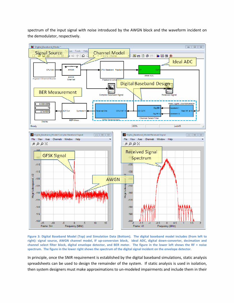
spectrum of the input signal with noise introduced by the AWGN block and the waveform incident on
the demodulator, respectively.
Figure 3: Digital Baseband Model (Top) and Simulation Data (Bottom). The digital baseband model includes (from left to
right): signal source, AWGN channel model, IF up-conversion block, ideal ADC, digital down-converter, decimation and
channel select filter block, digital envelope detector, and BER meter. The figure in the lower left shows the RF + noise
spectrum. The figure in the lower right shows the spectrum of the digital signal incident on the envelope detector.
In principle, once the SNIR requirement is established by the digital baseband simulations, static analysis
spreadsheets can be used to design the remainder of the system. If static analysis is used in isolation,
then system designers must make approximations to un-modeled impairments and include them in their
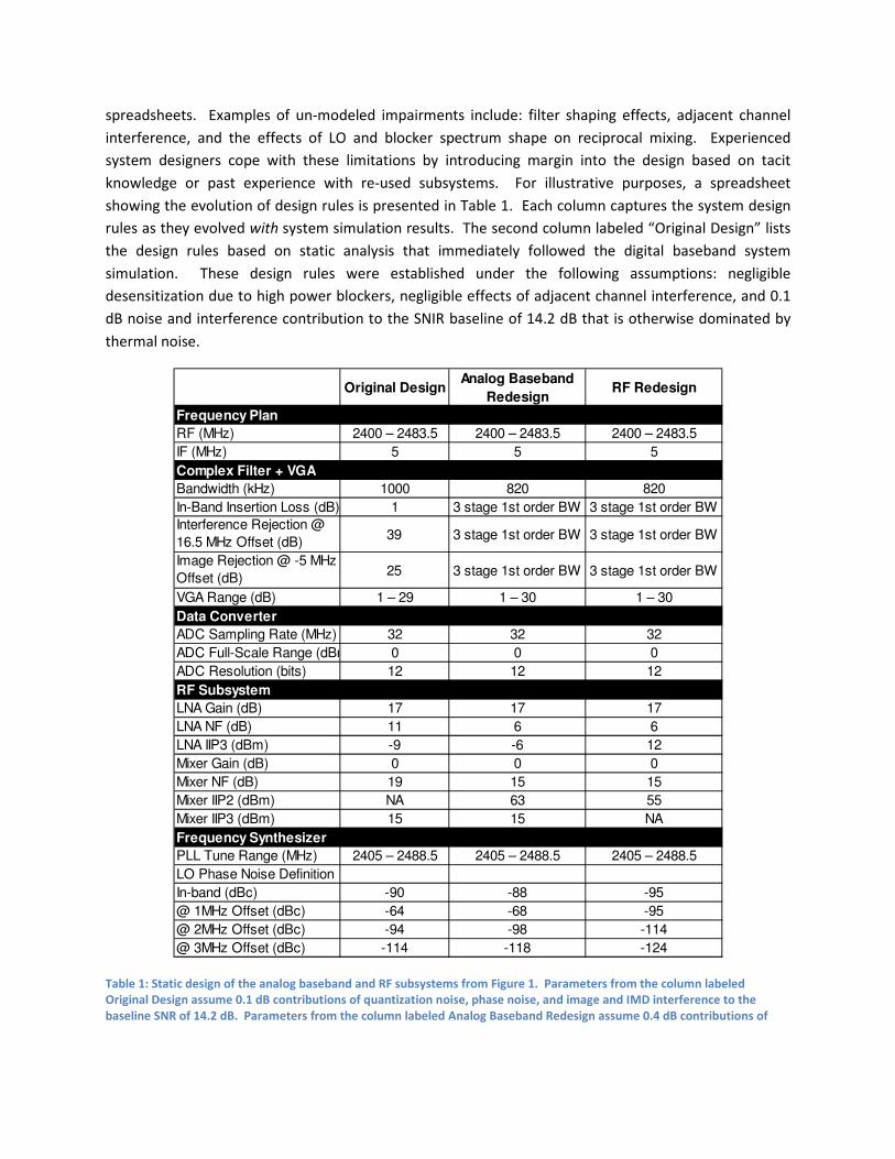
spreadsheets. Examples of un-modeled impairments include: filter shaping effects, adjacent channel
interference, and the effects of LO and blocker spectrum shape on reciprocal mixing. Experienced
system designers cope with these limitations by introducing margin into the design based on tacit
knowledge or past experience with re-used subsystems. For illustrative purposes, a spreadsheet
showing the evolution of design rules is presented in Table 1. Each column captures the system design
rules as they evolved with system simulation results. The second column labeled “Original Design” lists
the design rules based on static analysis that immediately followed the digital baseband system
simulation. These design rules were established under the following assumptions: negligible
desensitization due to high power blockers, negligible effects of adjacent channel interference, and 0.1
dB noise and interference contribution to the SNIR baseline of 14.2 dB that is otherwise dominated by
thermal noise.
Original DesignAnalog Baseband
RedesignRF Redesign
Frequency Plan
RF (MHz) 2400 – 2483.5 2400 – 2483.5 2400 – 2483.5
IF (MHz) 5 5 5
Complex Filter + VGA
Bandwidth (kHz) 1000 820 820
In-Band Insertion Loss (dB) 1 3 stage 1st order BW 3 stage 1st order BW
Interference Rejection @
16.5 MHz Offset (dB)39 3 stage 1st order BW 3 stage 1st order BW
Image Rejection @ -5 MHz
Offset (dB)25 3 stage 1st order BW 3 stage 1st order BW
VGA Range (dB) 1 – 29 1 – 30 1 – 30
Data Converter
ADC Sampling Rate (MHz) 32 32 32
ADC Full-Scale Range (dBm) 0 0 0
ADC Resolution (bits) 12 12 12
RF Subsystem
LNA Gain (dB) 17 17 17
LNA NF (dB) 11 6 6
LNA IIP3 (dBm) -9 -6 12
Mixer Gain (dB) 0 0 0
Mixer NF (dB) 19 15 15
Mixer IIP2 (dBm) NA 63 55
Mixer IIP3 (dBm) 15 15 NA
Frequency Synthesizer
PLL Tune Range (MHz) 2405 – 2488.5 2405 – 2488.5 2405 – 2488.5
LO Phase Noise Definition
In-band (dBc) -90 -88 -95
@ 1MHz Offset (dBc) -64 -68 -95
@ 2MHz Offset (dBc) -94 -98 -114
@ 3MHz Offset (dBc) -114 -118 -124
Table 1: Static design of the analog baseband and RF subsystems from Figure 1. Parameters from the column labeled
Original Design assume 0.1 dB contributions of quantization noise, phase noise, and image and IMD interference to the
baseline SNR of 14.2 dB. Parameters from the column labeled Analog Baseband Redesign assume 0.4 dB contributions of
thermal noise, quantization noise, phase noise, and image and IMD interference to the baseline SNR of 18.7 dB. The column
labeled RF Redesign captures the final set of design rules determined by complete system simulation.
Additional system simulation is used to test the feasibility of the design rules reported in the Original
Design column of Table 1. Following the design sequence from DSM 1, most of the analog baseband
subsystems are designed prior to the RF subsystem. The set of analog baseband subsystems in Figure 1
consist of a complex filter for image rejection and anti-aliasing, an IF amplifier, and finally a 12 bit ADC.
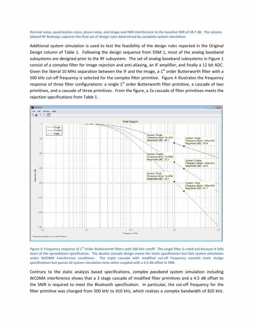
Given the liberal 10 MHz separation between the IF and the image, a 1st
order Butterworth filter with a
500 kHz cut-off frequency is selected for the complex filter primitive. Figure 4 illustrates the frequency
response of three filter configurations: a single 1st
order Butterworth filter primitive, a cascade of two
primitives, and a cascade of three primitives. From the figure, a 2x cascade of filter primitives meets the
rejection specifications from Table 1.
Figure 4: Frequency response of 1st
Order Butterworth filters with 500 kHz cutoff. The single filter is ruled out because it falls
short of the spreadsheet specification. The double cascade design meets the static specification but fails system simulation
under WCDMA interference conditions. The triple cascade with modified cut-off frequency exceeds static design
specifications but passes all system simulation tests when coupled with a 4.5 dB offset in SNR.
Contrary to the static analysis based specifications, complex passband system simulation including
WCDMA interference shows that a 3 stage cascade of modified filter primitives and a 4.5 dB offset to
the SNIR is required to meet the Bluetooth specification. In particular, the cut-off frequency for the
filter primitive was changed from 500 kHz to 410 kHz, which realizes a complex bandwidth of 820 kHz.
See Figure 5 for the block diagrams of the complex passband testbench and the filter primitive. Notice
that the filter primitive is described without reference to the actual implementation. This strategic
information hiding enables the system engineer to fully specify the filter shape without concern for the
actual filter implementation. Likewise, the downstream filter designer receives a meaningful
specification without the need to perform detailed system simulation to verify his design.
For the ADC, a sampling rate of 32 MHz ensures greater than four times oversampling of the filtered IF
waveform. Moreover, system simulation shows that an analog to digital converter with 12 bits of
resolution (i.e. 74 dB dynamic range) and 0dBm full-scale power requires a signal power level of -45 dBm
to meet the BER specification. In comparison, the quantization noise from system simulation need only
be 10.3 dB below the thermal noise floor, as opposed to the 16 dB that is determined by the general 0.1
dB heuristic captured in the static analysis and reported elsewhere [4].
The spectrum of the intermediate signals from the analog baseband simulations are shown on the graph
in lower right corner of Figure 5. Channel 1 shows the spectrum of the complex signal before the
polyphase filter whereas Channel 2 shows the spectrum of the signal immediately after the ADC. From
left to right, Channel 1 shows the image signal, the effect of WCDMA interference via even order IMD,
the desired Bluetooth signal, and the 3 MHz offset Bluetooth interference. By comparing Channel 1 with
Channel 2 it can be seen that the power in both the Bluetooth interference and the baseband IMD have
been significantly reduced by the analog baseband filter. See the column labeled “Analog Baseband
Redesign” in Table 1 for the new set of design rules determined by system simulation of both the analog
and digital subsystems.
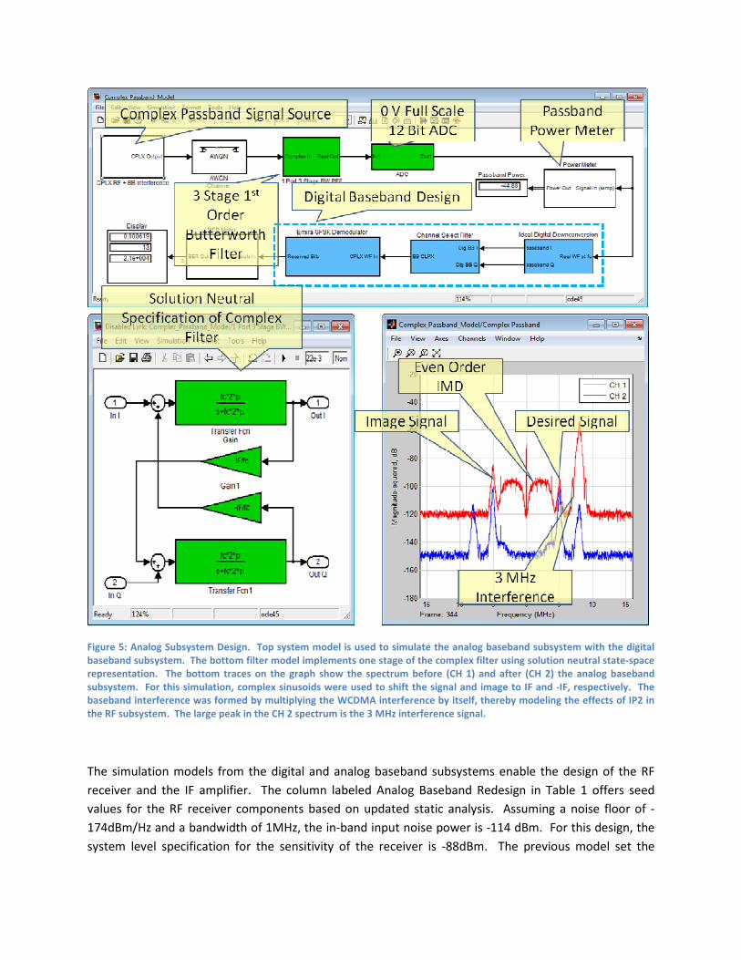
Figure 5: Analog Subsystem Design. Top system model is used to simulate the analog baseband subsystem with the digital
baseband subsystem. The bottom filter model implements one stage of the complex filter using solution neutral state-space
representation. The bottom traces on the graph show the spectrum before (CH 1) and after (CH 2) the analog baseband
subsystem. For this simulation, complex sinusoids were used to shift the signal and image to IF and -IF, respectively. The
baseband interference was formed by multiplying the WCDMA interference by itself, thereby modeling the effects of IP2 in
the RF subsystem. The large peak in the CH 2 spectrum is the 3 MHz interference signal.
The simulation models from the digital and analog baseband subsystems enable the design of the RF
receiver and the IF amplifier. The column labeled Analog Baseband Redesign in Table 1 offers seed
values for the RF receiver components based on updated static analysis. Assuming a noise floor of -
174dBm/Hz and a bandwidth of 1MHz, the in-band input noise power is -114 dBm. For this design, the
system level specification for the sensitivity of the receiver is -88dBm. The previous model set the
minimum SNIR to 18.7dB. Therefore, in the absence of interference the maximum noise figure for the
receiver design is 7.3 dB. Budgeting the noise contributions among the RF components is a trivial task
that is easily handled by static analysis tools. Similarly, once the system IP3 is known, static analysis can
be used to partition the interference sources among the receiver components.
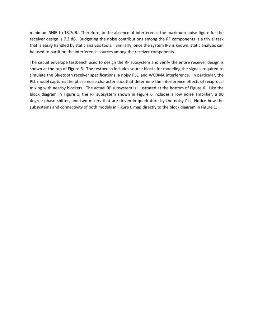
The circuit envelope testbench used to design the RF subsystem and verify the entire receiver design is
shown at the top of Figure 6. The testbench includes source blocks for modeling the signals required to
simulate the Bluetooth receiver specifications, a noisy PLL, and WCDMA interference. In particular, the
PLL model captures the phase noise characteristics that determine the interference effects of reciprocal
mixing with nearby blockers. The actual RF subsystem is illustrated at the bottom of Figure 6. Like the
block diagram in Figure 1, the RF subsystem shown in Figure 6 includes a low noise amplifier, a 90
degree phase shifter, and two mixers that are driven in quadrature by the noisy PLL. Notice how the
subsystems and connectivity of both models in Figure 6 map directly to the block diagram in Figure 1.
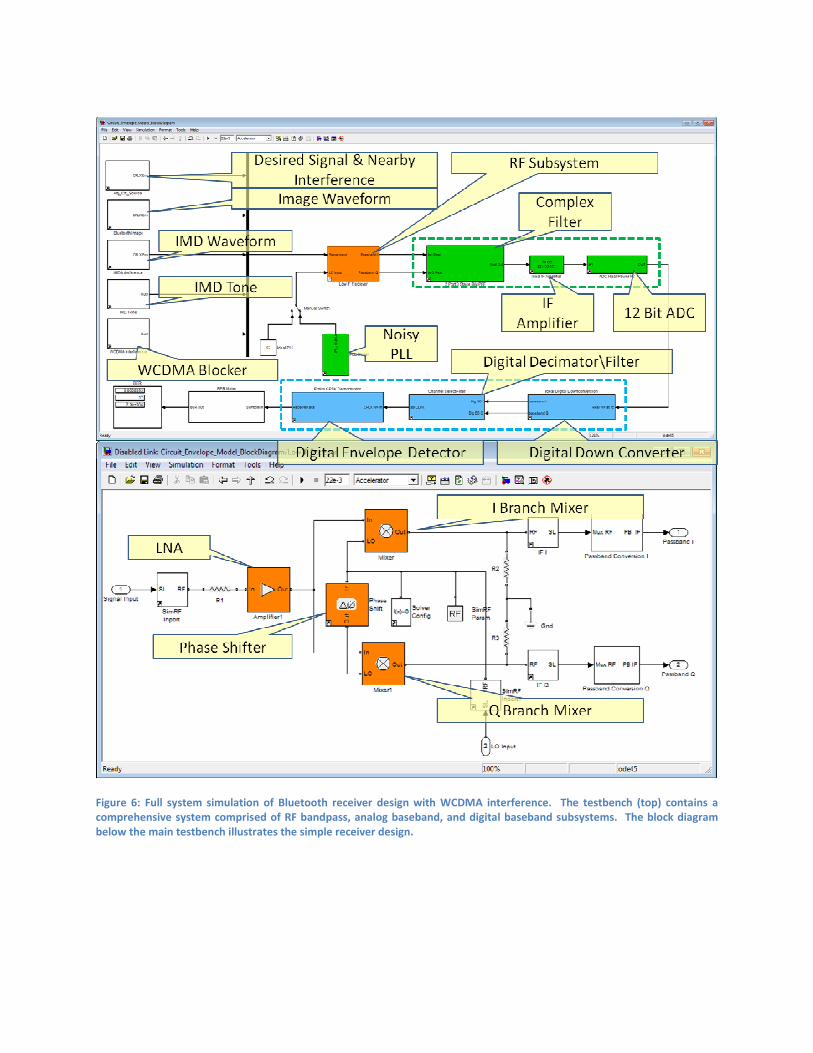
Figure 6: Full system simulation of Bluetooth receiver design with WCDMA interference. The testbench (top) contains a
comprehensive system comprised of RF bandpass, analog baseband, and digital baseband subsystems. The block diagram
below the main testbench illustrates the simple receiver design.
Figure 7: System Simulation Data. The spectrum of the input waveforms is shown in the graphs in the top row. For circuit
envelope simulation each of the input waveforms is assigned to a separate carrier. The bottom row shows plots of the
spectrum associated with the analog baseband and digital baseband waveforms. CH 1 on the left graph shows the analog
baseband waveform immediately following the RF receiver. CH 2 shows the spectrum of the analog baseband signal after
the filter and ADC. The figure on the right shows the spectrum of the signal just before the envelope detector.
The IF-amplifier gain is chosen to meet the ADC signal power (-45 dBm) determined by the analog
baseband design step. The final design rules are listed in the last column of Table 1 labeled “RF
Redesign”. Comparison of the three columns of Table 1 shows the convergence of the design rules to a
set of compliant specifications. The BER performance of the receiver design, from digital baseband to
RF, in the presence of WCDMA interference is captured in Table 2. Table 2 clearly shows that the design
meets the Bluetooth specifications with -88dBm sensitivity and in the presence of WCDMA interference.
Close examination of the table reveals the active constraints that heavily influenced the receiver design
rules. Namely, the non-zero BER suggests that this design was shaped largely by the sensitivity
specification and the 2 and 3 MHz interference specifications. What’s not shown in the table is the fact
that the design rules for a similar receiver with the same sensitivity requirement but without WCDMA
interference are indeed very different.
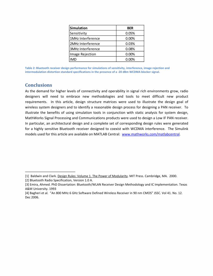
Simulation BER
Sensitivity 0.05%
1MHz Interference 0.00%
2MHz Interference 0.03%
3MHz Interference 0.08%
Image Rejection 0.00%
IMD 0.00%
Table 2: Bluetooth receiver design performance for simulations of sensitivity, interference, image rejection and
intermodulation distortion standard specifications in the presence of a -20 dBm WCDMA blocker signal.
Conclusions As the demand for higher levels of connectivity and operability in signal rich environments grow, radio
designers will need to embrace new methodologies and tools to meet difficult new product
requirements. In this article, design structure matrices were used to illustrate the design goal of
wireless system designers and to identify a reasonable design process for designing a PAN receiver. To
illustrate the benefits of using simulation tools in conjunction with static analysis for system design,
MathWorks Signal Processing and Communications products were used to design a Low IF PAN receiver.
In particular, an architectural design and a complete set of corresponding design rules were generated
for a highly sensitive Bluetooth receiver designed to coexist with WCDMA interference. The Simulink
models used for this article are available on MATLAB Central: www.mathworks.com/matlabcentral.
[1] Baldwin and Clark. Design Rules: Volume 1. The Power of Modularity. MIT Press. Cambridge, MA. 2000.
[2] Bluetooth Radio Specification, Version 1.0 A.
[3] Emira, Ahmed. PhD Dissertation: Bluetooth/WLAN Receiver Design Methodology and IC Implementation. Texas
A&M University. 1993
[4] Bagheri et al. ”An 800 MHz 6 GHz Software Defined Wireless Receiver in 90 nm CMOS” JSSC. Vol 41. No. 12.
Dec 2006.