Embed Size (px)
DESCRIPTION
CO Unit - II
Citation preview
Mailam Engineering College(Approved by AICTE, New Delhi, Affiliated to Anna University, Chennai & Accredited by
National Board of Accreditation (NBA), New Delhi)Mailam (Po), Villupuram (Dt). Pin: 604 304
DEPARTMENT OF COMPUTER APPLICATIONS
Unit–II [2 & 16 Marks]
Subject Incharge HOD Principal
Mailam Engineering College
Subject Name: Computer Organization
Subject Code: MC9211
Year : 2012 – 2013
Semester: I
Prepared By: Ms. A. Subathra Devi, MCA, M.Phil.,

(Approved by AICTE, New Delhi, Affiliated to Anna University, Chennai& Accredited by National Board of Accreditation (NBA), New Delhi)Mailam (Po), Villupuram (Dt). Pin: 604 304
DEPARTMENT OF COMPUTER APPLICATIONS
Computer Organization – MC9211
Part – A
1.
UNIT II COMBINATIONAL AND SEQUENTIAL CIRCUITS
Design of Combinational Circuits – Adder / Subtracter – Encoder – Decoder – MUX / DEMUX – Comparators, Flip Flops – Triggering – Master – Slave Flip Flop – State Diagram and Minimization – Counters – Registers.

Unit- II
Digital system consists of arithmetic and logic circuit (Gates & Flip-flops). It is divided into two types of circuit.
Combinational logic circuit Sequential logic circuit
Combinational logic circuitThe Combinational logic circuit consists of logic gates whose output at any time depends only on the input values at that time.
Types of Combinational logic circuit:Adder
Half AdderFull Adder
SubtractorHalf SubtractorFull Subtractor
DecoderEncoderMultiplexerDe-multiplexerMagnitude Comparators
Sequential logic circuit:
In Sequential logic circuit output at any time depends on the present input values as well as past output values.
Type of Sequential logic circuitFlip-FlopsRegisterCountersTriggersState diagram of minimization
Block diagram of Combinational logic circuit:
.
.
.
.
.
.
n – Input variables
m – Output variables
Combinational
Logic
Circuit
The Combinational logic circuit whose output at any time depends only on the input values at that time. The Output of the Combinational logic circuit does not depend on the any past output values. It accepts ‘n’ input binary variables, and generate ‘m’ output binary variable.Procedures or Rules for design the Combinational logic circuit:From the given word descriptions of the problem identify the number of input variables and required output.
The input and output variables are assigned letter symbols.
Draw truth table that describes the operation of the circuit for different Combinational of input.
Write down the switching expression for the output.
Simplify the switching expression using K-map or algebraic.
Implement the simplified expression using logic gates.
Adder (Addition):Half Adder:The Combinational circuit which performs the arithmetic addition of two binary digits and produce Sum and Carry.
It has 2 inputs and 2 outputs.The Input variables are A & B.The Output variables are Sum (S) and Carry (C).
Step: 1Block diagram of Half Adder:
Step: 2Truth Table
A B SUM (S)
CARRY (C)
0 0 0 0
CARRY(C)
SUM(S)
Input variables
Output variables
Half
Adder
A
B

0
1
1
1
0
1
1
1
0
0
0
1
Step: 3K-Map for Sum & Carry:
Sum = AB’ + A’B
= A (+) B
K-Map for Carry:
Carry = AB
Step: 4Logical diagram of half adder
Full Adder:
The Combinational circuit which performs the arithmetic addition of three binary digits and produce Sum and Carry.
A’
B’ B
A
0 1
01
Rules:
AB’ + A’B = A (+) B
A’B’ + AB = A (+) B
A’
B’ B
A
0 0
10

It has 3 inputs and 2 outputs.The Input variables are A, B & CThe Output variables are Sum (S) and Carry (C).
Step: 1Block diagram of Half Adder:
Step: 2Truth Table
A B C SUM (S)
CARRY (C)
0
0
0
0
1
1
1
1
0
0
1
1
0
0
1
1
0
1
0
1
0
1
0
1
0
1
1
0
1
0
0
1
0
0
0
1
0
1
1
1
Step: 3K-Map for Sum & Carry
CARRY(C)
SUM(S)
Input variables
Output variables
Full
Adder
A
C
B

Sum = AB’C’ + A’B’C + ABC + A’BC’Carry = AC + AB + BCStep: 4Logical diagram of Sum & Carry.
Subtractor (Subtraction):Half Subtractor:The Combinational circuit which performs the arithmetic subtraction of two binary digits and produce Difference and Borrow.
It has 2 inputs and 2 outputs.The Input variables are A & B.The Output variables are Difference (Diff) and Borrow (Bow).
Step: 1Block diagram of Half Subtractor:
Bow
DiffInput
variables
Output variable
s
Half
Subtractor
A
B

Step: 2Truth Table
A B Diff Borrow
0
0
1
1
0
1
0
1
0
1
1
0
0
1
0
0
Step: 3K-Map for Difference:
Sum = AB’ + A’B
= A (+) B
K-Map for Borrow:
Carry = A’B
Step: 4Logical diagram of half Subtactor
A’
B’ B
A
0 1
01
Rules:
AB’ + A’B = A (+) B
A’B’ + AB = A (+) B
A’
B’ B
A
0 1
00
Diff = AB
Bow = A’B’

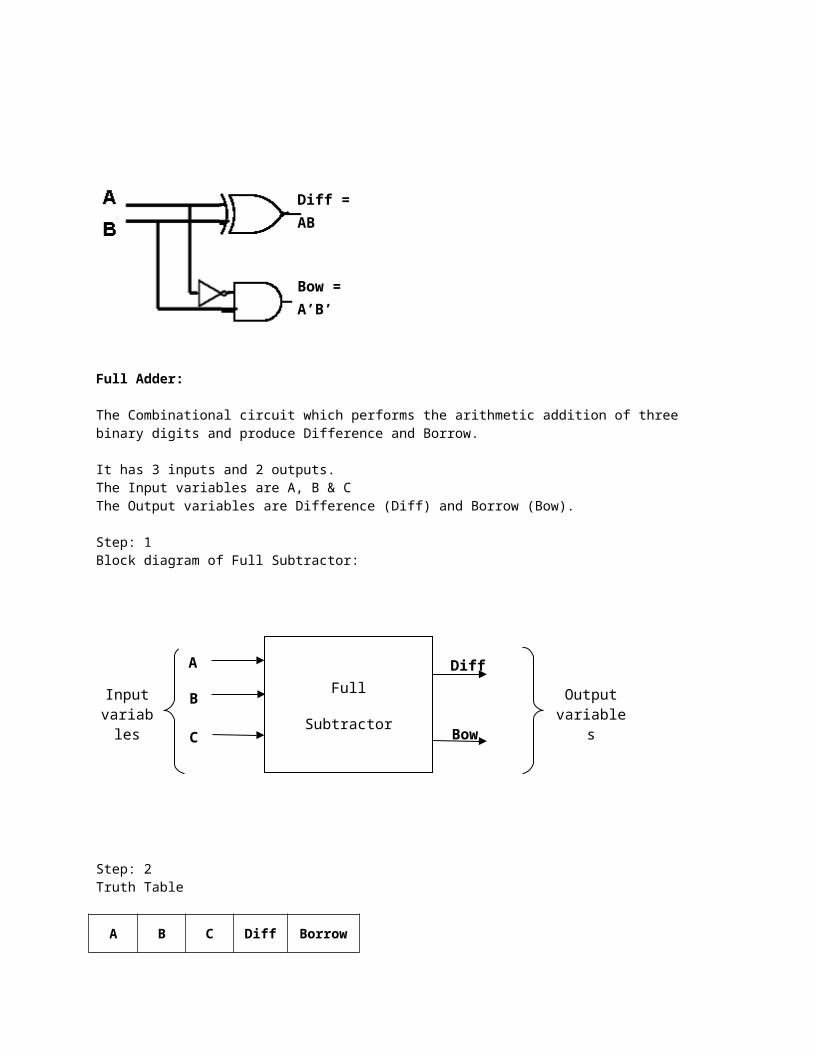
Full Adder:
The Combinational circuit which performs the arithmetic addition of three binary digits and produce Difference and Borrow.
It has 3 inputs and 2 outputs.The Input variables are A, B & CThe Output variables are Difference (Diff) and Borrow (Bow).
Step: 1Block diagram of Full Subtractor:
Step: 2Truth Table
A B C Diff Borrow
0
0
0
0
1
1
0
0
1
1
0
0
0
1
0
1
0
1
0
1
1
0
1
0
0
1
1
1
0
0
Bow
Diff
Input variables
Output variables
Full
Subtractor
A
C
B
1
1
1
1
0
1
0
1
0
1
Step: 3K-Map for Difference & Borrow:
Step: 4Logical diagram of Difference & Borrow:

Encoder:
An Encoder is a digital circuit that performs the inverse operation of a decoder. In encoder the output lines generates, the binary code corresponding to the input values.
Block diagram of Encoder:
For example take n=3, so inputs = 23 and output = 3
.
.
.
.
.
.
2n Input variables
n Output variables
Encoder
23 Input variables
3 Output variables
23 : 3
Encoder
D0
D1
D7
D2
D3
D4
D5
D6
A
B
C

Equation:
A = D4 + D5 + D6 + D7
B = D2 + D3 + D6 + D7
C = D1 + D3 + D5 + D7
Implementation of Encoder circuit:
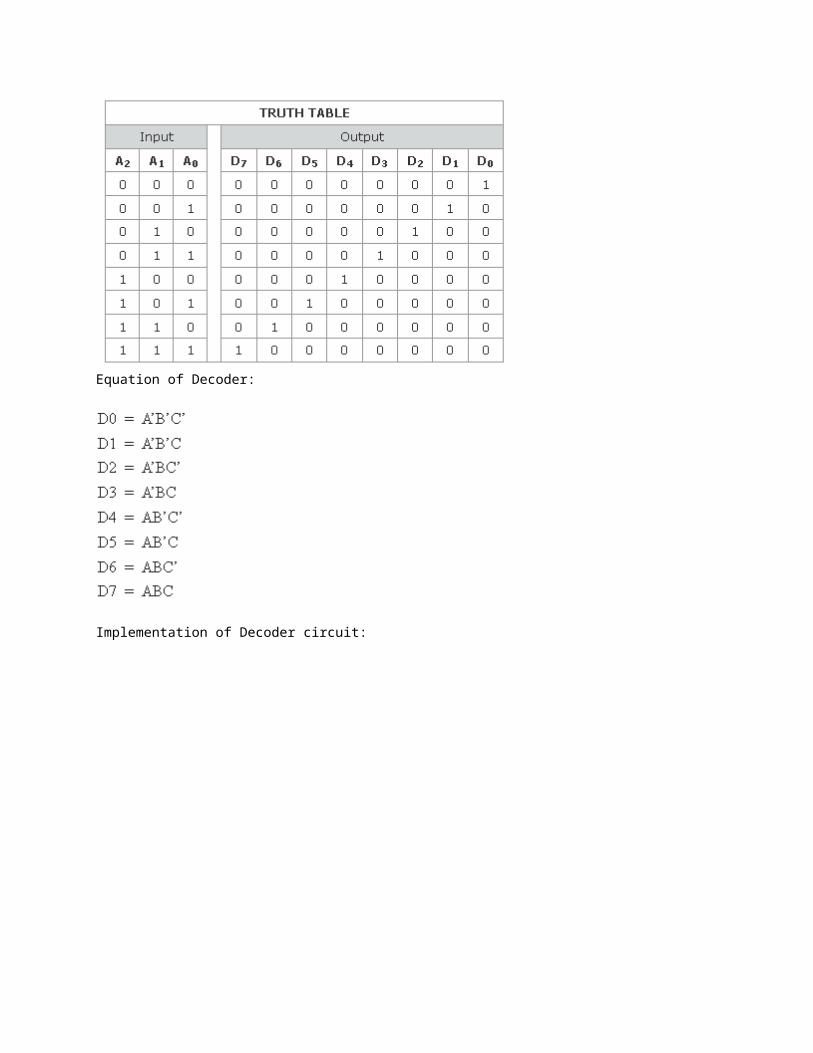
Decoder:

A Decoder is a logic circuit that converts an n-bit binary input code into 2n output lines, such that each output line will be activated for only one of the possible combination of inputs.
Block diagram of decoder:
For example take n=3, so inputs = 3 and output = 23
Truth table for Decoder
Equation of Decoder:
.
.
.
.
.
.
n Input variables
2n Output variables
Decoder
D0
D1
D7
D2
D3
D4
D5
D6
23 Input variables
3 Output variables
3 : 23
Decoder
A
B
C

Implementation of Decoder circuit:
MultiplexersThe Term ‘Multiplexer’ means many into one. Multiplexing is the process of transmitting a large number of information over a single line. A digital Multiplexer (MUX) is a combinational circuit that select one digital information from several sources and transmits the selected information on a single output line. It is otherwise called as data selector. It selects one of many inputs and steer the information to the output.
Normally, there are 2n inputs and n selected lines whose bit combine and determine which input is selected.
The Multiplexer is a very useful combinational device that has its uses in many different applications such as signal routing, data communications and data bus control. When used with a de-multiplexer, parallel data can be transmitted in serial form via a single data link such as a fiber-optic cable or telephone line. They can also be used to switch either analogue, digital or video signals, with the switching current in analogue power circuits limited to below 10mA to 20mA per channel in order to reduce heat dissipation.
Function Table:
= I0S’ + I1S
Logical Diagram:
Four : 1 MUX
It has four inputs I0 I1 I2 I3
S (Selected Input)
Input
0 I01 I1
0
1
MUX
I0
I1
S
Y
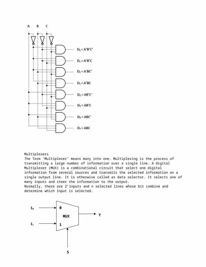
It has two selected inputs S0 S1
It has one output Y.
Block Diagram:
Function Table:
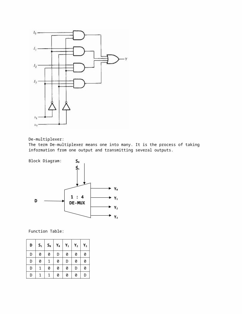
Y = I0S1’S0’ + I0S1’S0 + I1S1S0’ + I0S1S0
Logical Diagram:
S1 S0 Input
0 0 I00 1 I11 0 I21 1 I3
Y
0
1
4 : 1MUX
I0
I1
I2
I3
S1 S0

De-multiplexer:The term De-multiplexer means one into many. It is the process of taking information from one output and transmitting several outputs.
Block Diagram:
Function Table:
D S1 S0 Y0 Y1 Y2 Y3
D 0 0 D 0 0 0D 0 1 0 D 0 0D 1 0 0 0 D 0D 1 1 0 0 0 D
Y0 = DS1’S0’
Y1 = DS1’S0
S0 S1
1 : 4DE-MUX
Y0
Y1
Y2
Y3
D

Y2 = DS1S0’
Y3 = DS1S0
Logical Diagram:
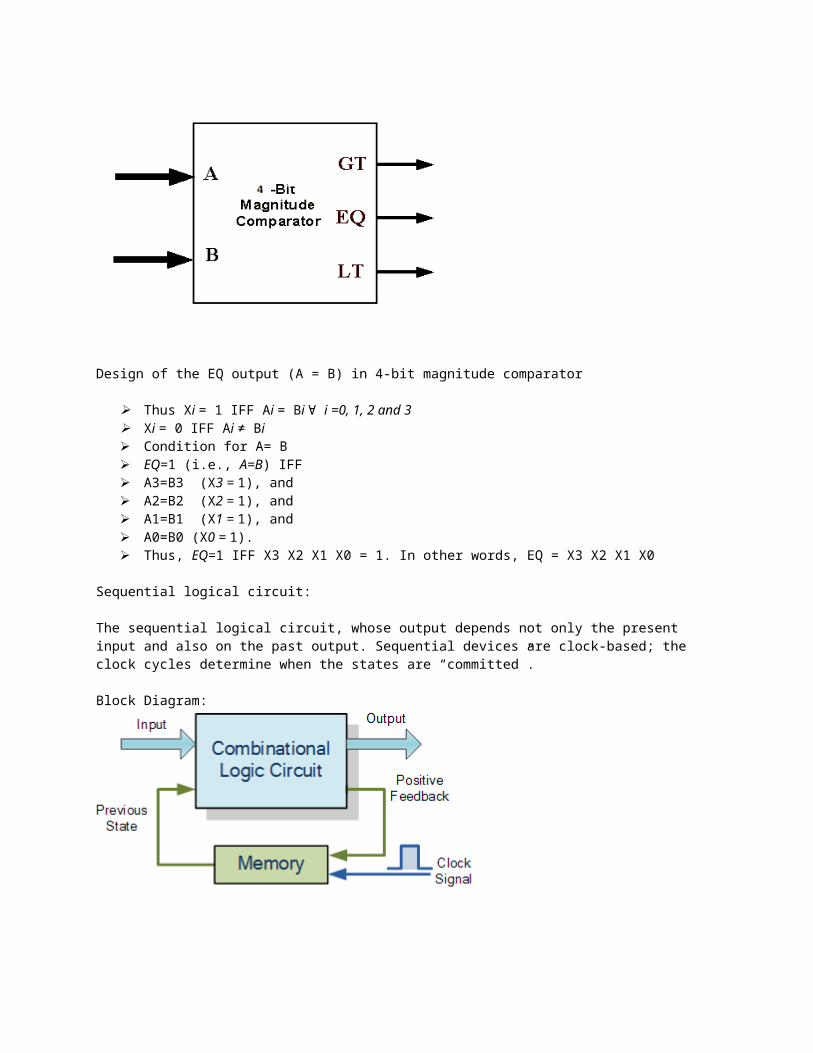
Magnitude comparator:
A digital comparator or magnitude comparator is a hardware electronic device that takes two numbers as input in binary form and determines whether one number is greater than, less than or equal to the other number. Comparators are used in a central processing units (CPU) and microcontrollers.
A magnitude comparator is a combinational circuit that compares two numbers A & B to determine whether:Type of Magnitude Comparator:
Two Bit Magnitude Comparator
A > B, or A = B, or A < B
Block Diagram:
3 output signals (GT, EQ, LT), where:
1. GT = 1 IFF A > B2. EQ = 1 IFF A = B3. LT = 1 IFF A < B
Note: Exactly One of these 3 outputs equals 1, while the other 2 outputs are 0`s
Four Bit Magnitude Comparator
Inputs: 8-bits (A ⇒ 4-bits , B ⇒ 4-bits) A and B are two 4-bit numbers Let A = A3, A2, A1, A0 and Let B = B3, B2, B1, B0 Inputs have 28 (256) possible combinations Not easy to design using conventional techniques
Design of the EQ output (A = B) in 4-bit magnitude comparator
Thus Xi = 1 IFF Ai = Bi ∀ i =0, 1, 2 and 3

Xi = 0 IFF Ai ≠ Bi Condition for A= B EQ=1 (i.e., A=B) IFF A3=B3 (X3 = 1), and A2=B2 (X2 = 1), and A1=B1 (X1 = 1), and A0=B0 (X0 = 1). Thus, EQ=1 IFF X3 X2 X1 X0 = 1. In other words, EQ = X3 X2 X1 X0
Sequential logical circuit:
The sequential logical circuit, whose output depends not only the present input and also on the past output. Sequential devices are clock-based; the clock cycles determine when the states are “committed”.
Block Diagram:
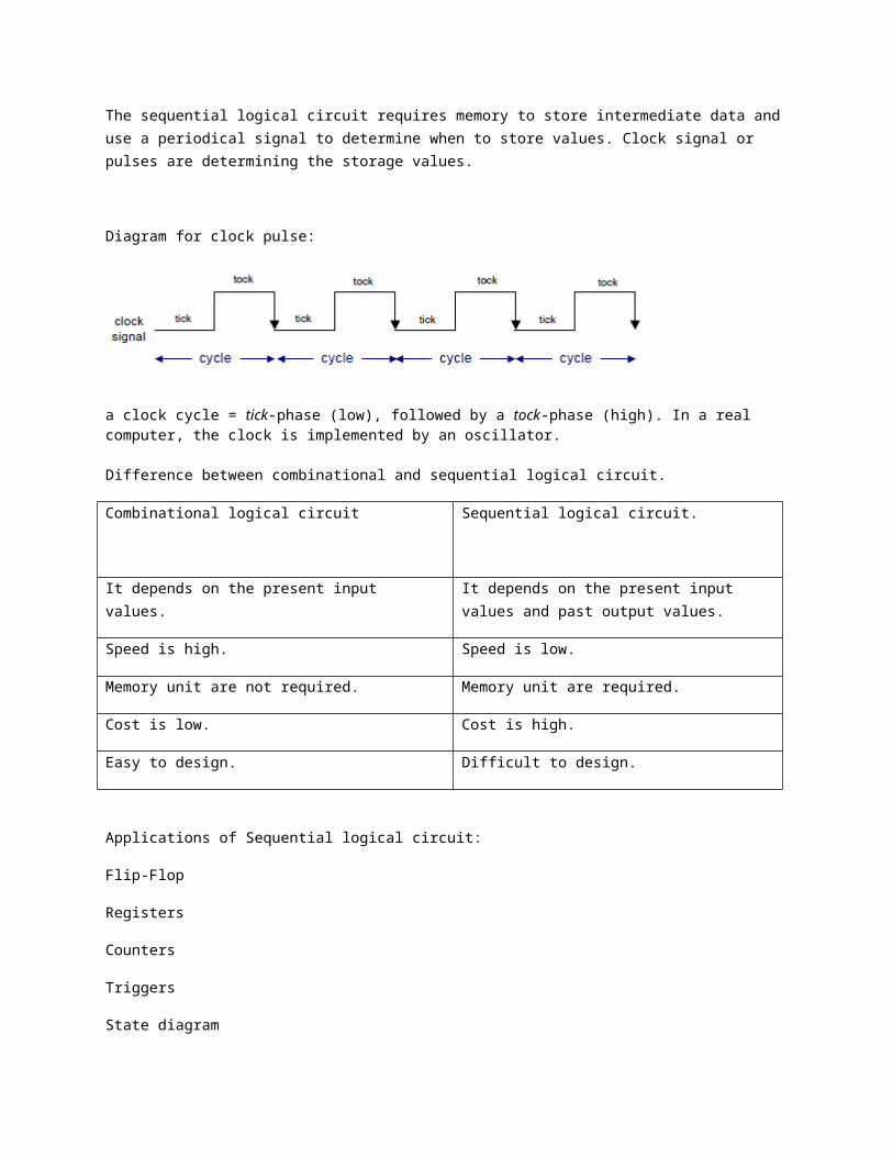
The sequential logical circuit requires memory to store intermediate data and use a periodical signal to determine when to store values. Clock signal or pulses are determining the storage values.
Diagram for clock pulse:
a clock cycle = tick-phase (low), followed by a tock-phase (high). In a real computer, the clock is implemented by an oscillator.
Difference between combinational and sequential logical circuit.
Combinational logical circuit Sequential logical circuit.

It depends on the present input values. It depends on the present input values and past output values.
Speed is high. Speed is low.
Memory unit are not required. Memory unit are required.
Cost is low. Cost is high.
Easy to design. Difficult to design.
Applications of Sequential logical circuit:
Flip-Flop
Registers
Counters
Triggers
State diagram
Flip-Flop:
The memory elements used in sequential circuit are called Flip-Flop. “A Flip-Flop circuit has two outputs, one for the normal value (1) and another for complement value (0) of the bit store in it. And input are depends upon the types of Flip-Flop”. It is otherwise called as Multi-Vibrators. Flip-flops and latches are a fundamental building block of digital electronics systems used in computers, communications, and many other types of systems.
Flip-flops and latches are used as data storage elements. Such data storage can be used for storage of state, and such a circuit is described as sequential logic. When used in a finite-state machine, the output and next state depend not only on its current input, but also on its current state. It can also be used for counting of pulses, and for synchronizing variably-timed input signals to some reference timing signal.
Block diagram:
Types of Flip-Flop:
It has four types in it. They are,
SR Flip-Flop
JK Flip-Flop
D Flip-Flop
T Flip-Flop
SR Flip-Flop:
The SR Flip-Flop has two inputs S (Set) and R (Reset). It has two outputs are Q (Normal) Q’ (Invertor).
Block Diagram:
Logical Diagram:
Rules:
When S = 0 and R = 0, the output Qn+1 in its Present State Qn ‘No Change‘.
When S = 0 and R = 1, the Flip-Flop ‘Reset’ to 0.
When S = 1 and R = 0, the Flip-Flop ‘Set’ to 1.
When S = 1 and R = 1, both the Qn+1 and Qn must be ‘indeterminate’ . Put Don’t care symbol ‘X’.
Characteristic Table:
Clock S R Present StateQn
Next StateQn+1
State
1 0 0 0 0No Change
1 0 0 1 1
1 0 1 0 0Reset
1 0 1 1 0
1 1 0 0 1Set
1 1 0 1 1
1 1 1 0 XIndeterminate
1 1 1 1 X
Implementation of Qn+1 into K-Map:
Extension Table:
Qn Qn+1 S R
0 0 0 X
0 1 1 0
1 0 0 1
1 1 X 0

State diagram of SR Flip-Flop:
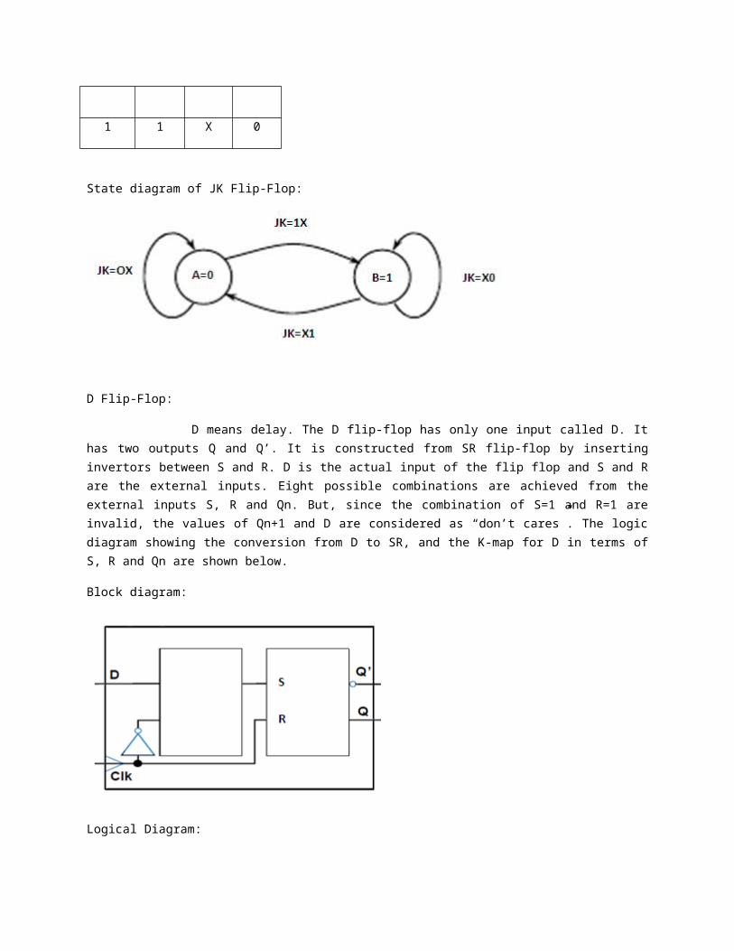
JK Flip-Flop:
JK means Jack Kilby, who is invented JK Flip-Flop is similar to SR Flip-Flop. It has two inputs J (Set) and K (Reset). It has four actions in it. This simple JK flip-Flop is the most widely used of all the flip-flop designs and is considered to be a universal flip-flop circuit.
Block diagram of JK Flip-Flop:
Logical Diagram:
Rules:
When J= 0 and K = 0, means ‘No Change‘.
When J= 0 and K = 1, means ‘Reset’ to 0.
When J= 1 and K = 0, means ‘Set’ to 1.

When J= 1 and K = 1, means ‘Toggle’.
Characteristic Table:
Clock J KPresent State
Qn
Next StateQn+1
State
1 0 0 0 0No Change
1 0 0 1 1
1 0 1 0 0Reset
1 0 1 1 0
1 1 0 0 1Set
1 1 0 1 1
1 1 1 0 1Toggle
1 1 1 1 0
Implementation of Qn+1 into K-Map:
Extension Table:
Qn Qn+1 S R
0 0 0 X
0 1 1 X
1 0 X 1
1 1 X 0

State diagram of JK Flip-Flop:
D Flip-Flop:
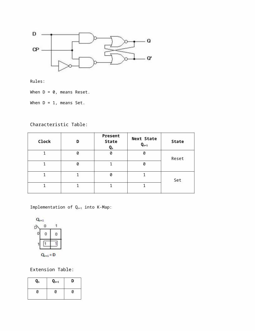
D means delay. The D flip-flop has only one input called D. It has two outputs Q and Q’. It is constructed from SR flip-flop by inserting invertors between S and R. D is the actual input of the flip flop and S and R are the external inputs. Eight possible combinations are achieved from the external inputs S, R and Qn. But, since the combination of S=1 and R=1 are invalid, the values of Qn+1 and D are considered as “don’t cares”. The logic diagram showing the conversion from D to SR, and the K-map for D in terms of S, R and Qn are shown below.
Block diagram:
Logical Diagram:
Rules:

When D = 0, means Reset.
When D = 1, means Set.
Characteristic Table:
Clock DPresent State
Qn
Next StateQn+1
State
1 0 0 0Reset
1 0 1 0
1 1 0 1Set
1 1 1 1
Implementation of Qn+1 into K-Map:
Extension Table:
Qn Qn+1 D
0 0 0
0 1 1
1 0 0
1 1 0
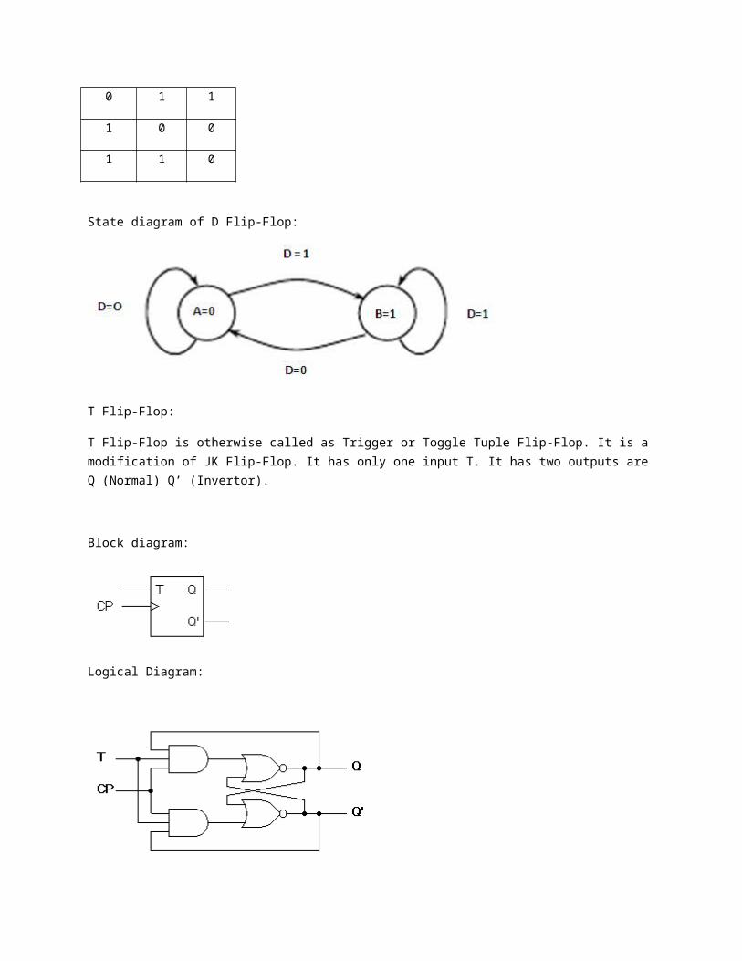
State diagram of D Flip-Flop:

T Flip-Flop:
T Flip-Flop is otherwise called as Trigger or Toggle Tuple Flip-Flop. It is a modification of JK Flip-Flop. It has only one input T. It has two outputs are Q (Normal) Q’ (Invertor).
Block diagram:
Logical Diagram:
Rules:
When T = 0, means ‘No change’.
When T = 1, means ‘Toggle’ (Complement).
Characteristic Table:
Clock t Present Next State State
StateQn
Qn+1
1 0 0 0No change
1 0 1 0
1 1 0 1Toggle
1 1 1 1
Implementation of Qn+1 into K-Map:
Extension Table:
Qn Qn+1 T
0 0 0
0 1 1
1 0 1
1 1 0
State diagram of D Flip-Flop:
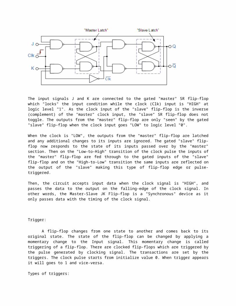
The Master-Slave Flip-flop
The Master-Slave Flip-Flop is basically two gated SR flip-flops connected together in a series configuration with the slave having an inverted clock pulse. The outputs from Q and Q from the "Slave" flip-flop are fed back to the inputs of the "Master" with the outputs of the "Master" flip-flop being connected to the two inputs of the "Slave" flip-flop. This feedback configuration from the slave's output to the master's input gives the characteristic toggle of the JK flip-flop as shown below.
Block diagram:
Logical diagram Master-Slave Flip-Flop
The input signals J and K are connected to the gated "master" SR flip-flop which "locks" the input condition while the clock (Clk) input is "HIGH" at logic level "1". As the clock input of the "slave" flip-flop is the inverse (complement) of the "master" clock input, the "slave" SR flip-flop does not toggle. The outputs from the "master" flip-flop are only "seen" by the gated "slave" flip-flop when the clock input goes "LOW" to logic level "0".
When the clock is "LOW", the outputs from the "master" flip-flop are latched and any additional changes to its inputs are ignored. The gated "slave" flip-flop now responds to the state of its inputs passed over by the "master" section. Then on the "Low-to-High" transition of the clock pulse the inputs of the "master" flip-flop are fed through to the gated inputs of the "slave" flip-flop and on the "High-to-Low" transition the same inputs are reflected on the output of the "slave" making this type of flip-flop edge or pulse-triggered.
Then, the circuit accepts input data when the clock signal is "HIGH", and passes the data to the output on the falling-edge of the clock signal. In other words, the Master-Slave JK Flip-flop is a "Synchronous" device as it only passes data with the timing of the clock signal.
Trigger:
A flip-flop changes from one state to another and comes back to its original state. The state of the flip-flop can be changed by applying a momentary change to the Input signal. This momentary change is called triggering of a flip-flop. There are clocked flip-flops which are triggered by the pulse generated by clocking signal. The transactions are set by the triggers. The clock pulse starts from initialize value 0. When trigger appears it will goes to 1 and vice-versa.
Types of triggers:
There are three types,
Level triggering
Edge triggering
Pulse triggering
Each trigger has two types in it. They are,
+ve triggering:
If the Flip-Flop changes it states when the clock is Positive.
–ve triggering:
If the Flip-Flop changes it states when the clock is Negative.
Level Triggering:
Level triggered flip-flops are dependent on the period of the pulse applied to it. If a flip-flop changes its state when the clock pulse applied is positive then it is called as positive level triggering. If the flip-flop changes its state when the clock pulse applied is negative then it is called negative level triggering.
Edge Triggering
The edge triggered flip flops changes state either at positive edges or negative edges of the clock pulse applied and accordingly they are classified into Positive edge triggered Flip flops and Negative edge triggered flip flops. A positive or rising transition is achieved from positive edge flip flops and negative or falling transition is achieved from negative edge flip flops.
Pulse Triggering:
The term pulse-triggered means that data are entered into the flip-flop on the rising edge of the clock pulse, but the output does not reflect the input state until the falling edge of the clock pulse. As this kind of flip-flops are sensitive to any change of the input levels during

the clock pulse is still HIGH, the inputs must be set up prior to the clock pulse's rising edge and must not be changed before the falling edge.
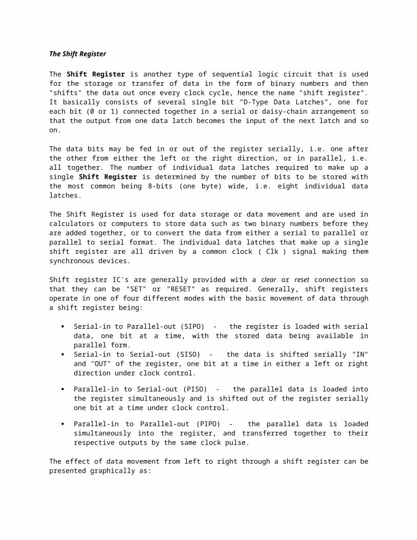
The Shift Register
The Shift Register is another type of sequential logic circuit that is used for the storage or transfer of data in the form of binary numbers and then "shifts" the data out once every clock cycle, hence the name "shift register". It basically consists of several single bit "D-Type Data Latches", one for each bit (0 or 1) connected together in a serial or daisy-chain arrangement so that the output from one data latch becomes the input of the next latch and so on.
The data bits may be fed in or out of the register serially, i.e. one after the other from either the left or the right direction, or in parallel, i.e. all together. The number of individual data latches required to make up a single Shift Register is determined by the number of bits to be stored with the most common being 8-bits (one byte) wide, i.e. eight individual data latches.
The Shift Register is used for data storage or data movement and are used in calculators or computers to store data such as two binary numbers before they are added together, or to convert the data from either a serial to parallel or parallel to serial format. The individual data latches that make up a single shift register are all driven by a common clock ( Clk ) signal making them synchronous devices.
Shift register IC's are generally provided with a clear or reset connection so that they can be "SET" or "RESET" as required. Generally, shift registers operate in one of four different modes with the basic movement of data through a shift register being:
Serial-in to Parallel-out (SIPO) - the register is loaded with serial data, one bit at a time, with the stored data being available in parallel form.
Serial-in to Serial-out (SISO) - the data is shifted serially "IN" and "OUT" of the register, one bit at a time in either a left or right direction under clock control.
Parallel-in to Serial-out (PISO) - the parallel data is loaded into the register simultaneously and is shifted out of the register serially one bit at a time under clock control.
Parallel-in to Parallel-out (PIPO) - the parallel data is loaded simultaneously into the register, and transferred together to their respective outputs by the same clock pulse.
The effect of data movement from left to right through a shift register can be presented graphically as:

Also, the directional movement of the data through a shift register can be either to the left, (left shifting) to the right, (right shifting) left-in but right-out, (rotation) or both left and right shifting within the same register thereby making it bidirectional. In this tutorial it is assumed that all the data shifts to the right, (right shifting).
Serial-in to Parallel-out (SIPO)
4-bit Serial-in to Parallel-out Shift Register
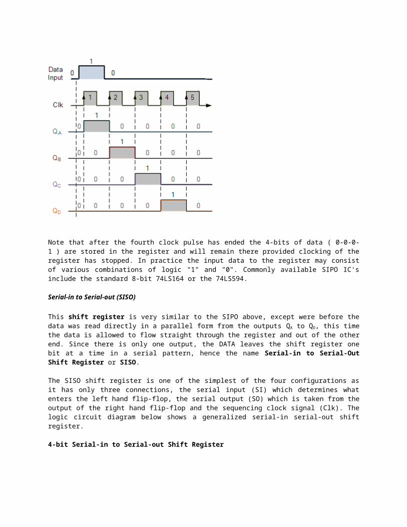
The operation is as follows. Lets assume that all the flip-flops ( FFA to FFD ) have just been RESET ( CLEAR input ) and that all the outputs QA to QD are at logic level "0" i.e, no parallel data output. If a logic "1" is connected to the DATA input pin of FFA then on the first clock pulse the output of FFA and therefore the resulting QA will be set HIGH to logic "1" with all the other outputs still remaining LOW at logic "0". Assume now that the DATA input pin of FFA has returned LOW again to logic "0" giving us one data pulse or 0-1-0.
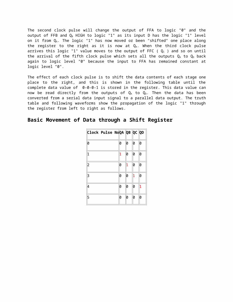
The second clock pulse will change the output of FFA to logic "0" and the output of FFB and QB HIGH to logic "1" as its input D has the logic "1" level on it from QA. The logic "1" has now moved or been "shifted" one place along the register to the right as it is now at QA. When the third clock pulse arrives this logic "1" value moves to the output of FFC ( QC ) and so on
until the arrival of the fifth clock pulse which sets all the outputs QA to QD back again to logic level "0" because the input to FFA has remained constant at logic level "0".
The effect of each clock pulse is to shift the data contents of each stage one place to the right, and this is shown in the following table until the complete data value of 0-0-0-1 is stored in the register. This data value can now be read directly from the outputs of QA to QD. Then the data has been converted from a serial data input signal to a parallel data output. The truth table and following waveforms show the propagation of the logic "1" through the register from left to right as follows.
Basic Movement of Data through a Shift Register
Clock Pulse NoQAQBQCQD
0 0 0 0 0
1 1 0 0 0
2 0 1 0 0
3 0 0 1 0
4 0 0 0 1
5 0 0 0 0
Note that after the fourth clock pulse has ended the 4-bits of data ( 0-0-0-1 ) are stored in
the register and will remain there provided clocking of the register has stopped. In practice the input data to the register may consist of various combinations of logic "1" and "0". Commonly available SIPO IC's include the standard 8-bit 74LS164 or the 74LS594.
Serial-in to Serial-out (SISO)
This shift register is very similar to the SIPO above, except were before the data was read directly in a parallel form from the outputs QA to QD, this time the data is allowed to flow straight through the register and out of the other end. Since there is only one output, the DATA leaves the shift register one bit at a time in a serial pattern, hence the name Serial-in to Serial-Out Shift Register or SISO.
The SISO shift register is one of the simplest of the four configurations as it has only three connections, the serial input (SI) which determines what enters the left hand flip-flop, the serial output (SO) which is taken from the output of the right hand flip-flop and the sequencing clock signal (Clk). The logic circuit diagram below shows a generalized serial-in serial-out shift register.
4-bit Serial-in to Serial-out Shift Register
You may think what's the point of a SISO shift register if the output data is exactly the same as the input data. Well this type of Shift Register also acts as a temporary storage device or as a time delay device for the data, with the amount of time delay being controlled by the number of stages in the register, 4, 8, 16 etc or by varying the application of the clock pulses. Commonly available IC's include the 74HC595 8-bit Serial-in/Serial-out Shift Register all with 3-state outputs.
Parallel-in to Serial-out (PISO)
The Parallel-in to Serial-out shift register acts in the opposite way to the serial-in to parallel-out one above. The data is loaded into the register in a parallel format i.e. all the data bits enter their inputs simultaneously, to the parallel input pins PA to PD of the register. The data is then read out sequentially in the normal shift-right mode from the register at Q representing the data present at PA to PD.
This data is outputted one bit at a time on each clock cycle in a serial format. It is important to note that with this system a clock pulse is not required to parallel load the register as it is already present, but four clock pulses are required to unload the data.
4-bit Parallel-in to Serial-out Shift Register
As this type of shift register converts parallel data, such as an 8-bit data word into serial format, it can be used to multiplex many different input lines into a single serial DATA stream which can be sent directly to a computer or transmitted over a communications line. Commonly available IC's include the 74HC166 8-bit Parallel-in/Serial-out Shift Registers.
Parallel-in to Parallel-out (PIPO)
The final mode of operation is the Parallel-in to Parallel-out Shift Register. This type of register also acts as a temporary storage device or as a time delay device similar to the SISO configuration above. The data is presented in a parallel format to the parallel input pins PA to PD and then transferred together directly to their respective output pins QA to QA by the same clock pulse. Then one clock pulse loads and unloads the register. This arrangement for parallel loading and unloading is shown below.
4-bit Parallel-in to Parallel-out Shift Register
The PIPO shift register is the simplest of the four configurations as it has only three connections, the parallel input (PI) which determines what enters the flip-flop, the parallel output (PO) and the sequencing clock signal (Clk).

Similar to the Serial-in to Serial-out shift register, this type of register also acts as a temporary storage device or as a time delay device, with the amount of time delay being varied by the frequency of the clock pulses. Also, in this type of register there are no interconnections between the individual flip-flops since no serial shifting of the data is required.
Universal Shift Register
Today, high speed bi-directional "universal" type Shift Registers such as the TTL 74LS194, 74LS195 or the CMOS 4035 are available as a 4-bit multi-function devices that can be used in either serial-to-serial, left shifting, right shifting, serial-to-parallel, parallel-to-serial, and as a parallel-to-parallel multifunction data register, hence the name "Universal". These devices can perform any combination of parallel and serial input to output operations but require additional inputs to specify desired function and to pre-load and reset the device.
4-bit Universal Shift Register 74LS194
Universal shift registers are very useful digital devices. They can be configured to respond to operations that require some form of temporary memory, delay information such as the SISO or PIPO configuration modes or transfer data from one point to another in either a serial or parallel format. Universal shift registers are frequently used in arithmetic operations to shift data to the left or right for multiplication or division.
The Ring Counter
In the previous Shift Register tutorial we saw that if we apply a serial data signal to the input of a serial-in to serial-out shift register, the same sequence of data will exit from the last flip-flip in the register chain after a preset number of clock cycles thereby acting as a sort of time delay circuit to the original signal.
But what if we were to connect the output of this shift register back to its input so that the output from the last flip-flop, QD becomes the input of the first flip-flop, DA. We would then have a closed loop circuit that "recirculates" the DATA around a continuous loop for every state of its sequence, and this is the principal operation of a Ring Counter. Then by looping the output back to the input, we can convert a standard shift register into a ring counter. Consider the circuit below.
4-bit Ring Counter
The synchronous Ring Counter example above, is preset so that exactly one data bit in the register is set to logic "1" with all the other bits reset to "0". To achieve this, a "CLEAR" signal is firstly applied to all the flip-flops together in order to "RESET" their outputs to a logic "0" level and then a "PRESET" pulse is applied to the input of the first flip-flop ( FFA ) before the clock pulses are applied. This then places a single logic "1" value into the circuit of the ring counter.
So on each successive clock pulse, the counter circulates the same data bit between the four flip-flops over and over again around the "ring" every fourth clock cycle. But in order to cycle the data correctly around the counter we must first "load" the counter with a suitable data pattern as all logic "0's" or all logic "1's" outputted at each clock cycle would make the ring counter invalid.
This type of data movement is called "rotation", and like the previous shift register, the effect of the movement of the data bit from left to right through a ring counter can be presented graphically as follows along with its timing diagram:
Rotational Movement of a Ring Counter
Since the ring counter example shown above has four distinct states, it is also known as a "modulo-4" or "mod-4" counter with each flip-flop output having a frequency value equal to one-fourth or a quarter (1/4) that of the main clock frequency.
The "MODULO" or "MODULUS" of a counter is the number of states the counter counts or sequences through before repeating itself and a ring counter can be made to output any modulo number. A "mod-n" ring counter will require "n" number of flip-flops connected together to circulate a single data bit providing "n" different output states.
For example, a mod-8 ring counter requires eight flip-flops and a mod-16 ring counter would require sixteen flip-flops. However, as in our example above, only four of the possible sixteen states are used, making ring counters very inefficient in terms of their output state usage.
Johnson Ring Counter
The Johnson Ring Counter or "Twisted Ring Counters", is another shift register with feedback exactly the same as the standard Ring Counter above, except that this time the inverted output Q of the last flip-flop is now connected back to the input D of the first flip-flop as shown below.

The main advantage of this type of ring counter is that it only needs half the number of flip-flops compared to the standard ring counter then its modulo number is halved. So a "n-stage" Johnson counter will circulate a single data bit giving sequence of 2n different states and can therefore be considered as a "mod-2n counter".
4-bit Johnson Ring Counter
This inversion of Q before it is fed back to input D causes the counter to "count" in a different way. Instead of counting through a fixed set of patterns like the normal ring counter such as for a 4-bit counter, "0001"(1), "0010"(2), "0100"(4), "1000"(8) and repeat, the Johnson counter counts up and then down as the initial logic "1" passes through it to the right replacing the preceding logic "0".
A 4-bit Johnson ring counter passes blocks of four logic "0" and then four logic "1" thereby producing an 8-bit pattern. As the inverted output Q is connected to the input D this 8-bit pattern continually repeats. For example, "1000", "1100", "1110", "1111", "0111", "0011", "0001", "0000" and this is demonstrated in the following table below.
Truth Table for a 4-bit Johnson Ring Counter
Clock Pulse No FFA FFB FFC FFD
0 0 0 0 0
1 1 0 0 0
2 1 1 0 0
3 1 1 1 0

4 1 1 1 1
5 0 1 1 1
6 0 0 1 1
7 0 0 0 1
As well as counting or rotating data around a continuous loop, ring counters can also be used to detect or recognise various patterns or number values within a set of data. By connecting simple logic gates such as the AND or the OR gates to the outputs of the flip-flops the circuit can be made to detect a set number or value. Standard 2, 3 or 4-stage Johnson ring counters can also be used to divide the frequency of the clock signal by varying their feedback connections and divide-by-3 or divide-by-5 outputs are also available.
A 3-stage Johnson Ring Counter can also be used as a 3-phase, 120 degree phase shift square wave generator by connecting to the data outputs at A, B and NOT-B. The standard 5-stage Johnson counter such as the commonly available CD4017 is generally used as a synchronous decade counter/divider circuit. The smaller 2-stage circuit is also called a "Quadrature" (sine/cosine) Oscillator/Generator and is used to produce four individual outputs that are each "phase shifted" by 90 degrees with respect to each other, and this is shown below.
2-bit Quadrature Generator

Output A B C D
QA+QB 1 0 0 0
QA+QB 0 1 0 0
QA+QB 0 0 1 0
QA+QB 0 0 0 1
2-bit Quadrature Oscillator, Count Sequence
As the four outputs, A to D are phase shifted by 90 degrees with regards to each other, they can be used with additional circuitry, to drive a 2-phase full-step stepper motor for position control or the ability to rotate a motor to a particular location as shown below.
Stepper Motor Control

2-phase (unipolar) Full-Step Stepper Motor Circuit
The speed of rotation of the Stepper Motor will depend mainly upon the clock frequency and additional circuitry would be require to drive the "power" requirements of the motor. As this section is only intended to give the reader a basic understanding of Johnson Ring Counters and its applications, other good websites explain in more detail the types and drive requirements of stepper motors.
Johnson Ring Counters are available in standard TTL or CMOS IC form, such as the CD4017 5-Stage, decade Johnson ring counter with 10 active HIGH decoded outputs or the CD4022 4-stage, divide-by-8 Johnson counter with 8 active HIGH decoded outputs.