Embed Size (px)
Citation preview

CMP Scratches; Their Detection and
Analysis on Root Causes
6th LEVITRONIX CMP and Ultrapure Conference The Westin Park Central, Dallas, Texas
May 11-12, 2011
May 11, 2011
Jin-Goo Park
Department of Materials Engineering, Hanyang University, Ansan, 426-791, Korea

2 Nano-Bio Electronic Materials and Processing Lab. 6th LEVITRONIX CMP and Ultrapure Conference
Outline
Introduction
Issues of CMP Defects(Scratch)
Motivation
Experimental
Results
Summary
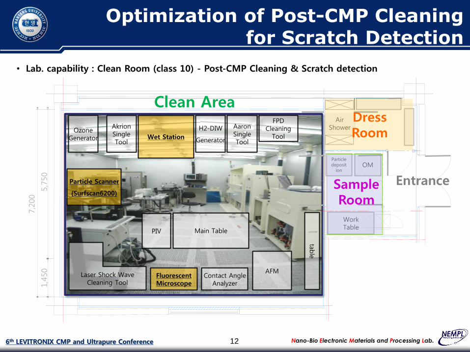
Lab. capability
Experiment tools & procedure
Post-CMP cleaning
Detection method of scratches
Scratch source & scratch shape (pad debris, dry particle, diamond particle)
Effect of Large Particle concentration
Effect of conditioner diamond

3 Nano-Bio Electronic Materials and Processing Lab. 6th LEVITRONIX CMP and Ultrapure Conference
ICPT 2011 in Seoul, Korea
• http://www.icpt2011.com/
• November 9 – 11, 2011
• Abstract due online July 4, 2011

4 Nano-Bio Electronic Materials and Processing Lab. 6th LEVITRONIX CMP and Ultrapure Conference
Scratch Sources in Oxide CMP
Polishing table
Polishing pad
Head
Pressure
Slurry
Conditioner Wafer
Slurry
Conditioner Surface
Pad Surface
CMP consumables : Pad, Slurry, Conditioner
These consumables should be controlled to achieve better performance

5 Nano-Bio Electronic Materials and Processing Lab. 6th LEVITRONIX CMP and Ultrapure Conference
The Migration of CMP Technology
CMP Tool
Polishing recipe
Pattern design
Slurry
Consumable part
Pressure control & table speed tuning
Chosen the tool equipped the head of retainer ring
and membrane
Applied optional slurry for
each process
Compounding the
consumable parts
AMAT MIRRA tool
CMP simulation & dummy
pattern insert
Removal profile & selectivity, dishing control
The alterative application of
consumable parts
Removal profile control

6 Nano-Bio Electronic Materials and Processing Lab. 6th LEVITRONIX CMP and Ultrapure Conference
The Type of defects Produced after oxide CMP
Surface
Void
Residual
Slurry Embedded
Particle
Scratch
Surface Particle
Common
CMP Defects
Scratch is the most deleterious defect compared to other type of defects.

7 Nano-Bio Electronic Materials and Processing Lab. 6th LEVITRONIX CMP and Ultrapure Conference
ITRS Roadmap
Micro-scratches and defects can lead to severe circuit failure, low yield and
potential reliability issue.
It is important to evaluate defects and their sources for CMP sustainability.
Among defects, scratch is still not well understood in CMP process

8 Nano-Bio Electronic Materials and Processing Lab. 6th LEVITRONIX CMP and Ultrapure Conference
The Factors that Play Key Role in the Scratch formation
Slurry
Pad
Conditioner
Wafer Surface
Wafer hardness : TEOS, HDP, BPSG
Abrasive size and Distribution
Large particle concentration
Abrasive type (Colloidal, Fumed, New type) and Agglomeration
Particle morphology
Diamond size & density
Diamond shape
Diamond patterns
Role of Active diamond
Diamond wearing or breaking
Pad asperity& contact area
Pad profile
Pad debris
Film Material : Cu, STI, ILD
Pad cutting rate
Design (asperities, pore and groove) Hardness

9 Nano-Bio Electronic Materials and Processing Lab. 6th LEVITRONIX CMP and Ultrapure Conference
Motivation
Detection of scratches formed on oxide wafer
Effect of CMP process and consumables
• CMP Process (pressure, velocity of head/platen)
• CMP Slurry
• CMP pad & conditioner
• Thin film materials
Study on Scratch
formation CMP
performance
To evaluate the post CMP cleaning process to detect the scratches
easily by a new technique

10 Nano-Bio Electronic Materials and Processing Lab. 6th LEVITRONIX CMP and Ultrapure Conference
Experimental (Modification of Polisher Head)
DOOPLA310 (300 mm) 12” Head 8” Head (scratch test)
• Modification and Installation of 8” polisher head for scratch
formation and detection

11 6th LEVITRONIX CMP and Ultrapure Conference Nano-Bio Electronic Materials and Processing Lab.
Experimental Procedure (Scratch Formation)
New Pad
Break-In
Conditioning
CMP
-Dummy (2)
- RR&N.U (2)
- Gathering (2)
-- Scratch (3)
Cleaning
Detection
Pad – IC1010
Break In
- Conditioning with DIW (30min)
- Conditioning with Slurry (10min)
Conditioning
- Conditioning with DIW (10min),
- Conditioning with Slurry (5min)
CMP
- Dummy CMP 2times
- CMP for CMP performance 2 times
- Dummy CMP for slurry gathering 2times
- CMP for scratch 3times
Cleaning
- SC-1 (10min)→Over Flower (3min) → DHF (3min)
→ Over Flower (210 Sec) → SC-1 (10min) → IPA Dry
Repeating
12 Nano-Bio Electronic Materials and Processing Lab. 6th LEVITRONIX CMP and Ultrapure Conference
Optimization of Post-CMP Cleaning for Scratch Detection
Contact Angle Analyzer
Wet Station Ozone
Generator
Aaron Single Tool
Particle Scanner
(Surfscan6200)
Laser Shock Wave Cleaning Tool
Fluorescent Microscope
AFM
H2-DIW
Generator
FPD Cleaning
Tool
table
Main Table PIV
Work Table
Particle deposit
ion OM
Air Shower Akrion
Single Tool
7,2
00 5
,750
1,4
50
• Lab. capability : Clean Room (class 10) - Post-CMP Cleaning & Scratch detection
Sample Room
Dress Room
Clean Area
Entrance

13 6th LEVITRONIX CMP and Ultrapure Conference Nano-Bio Electronic Materials and Processing Lab.
Analysis Tools for Scratch detection
Particle scanner
(Surfscan 6200, KLA-Tencor, USA)
• Surfscan6200 (KLA-Tencor)
: Detection of Scratch number
• Control the Gain value & Threshold value
Optical Microscope
(Nikon, LV-100D)
1000X 20μm
• Analysis of Scratch shape
• Counting the non-removed particle after cleaning
Defect number Scratch shape

14 6th LEVITRONIX CMP and Ultrapure Conference Nano-Bio Electronic Materials and Processing Lab.
Post-CMP Cleaning (Role of Scrubber Cleaning)
Wet Send
Indexer Brush
Module
DIW
1 min
Schematic of removal of particle
from surface by scrubber
A standard, hollow cylindrical
sponge with nodules
PVA Scrubber
• Scrubber Cleaning after slurry dipping during 1min
• PRE is increased by scrubber cleaning
0
5000
10000
15000
20000
No scrubber
LP
D (
ea)
Scrubber
Gain(4), Threshold(0.18)
: 0.18 um ~ 1.6 um
Gain(4), Threshold(0.36)
: 0.36 um ~ 1.6 um
Effect of Scrubber Cleaning

15 6th LEVITRONIX CMP and Ultrapure Conference Nano-Bio Electronic Materials and Processing Lab.
Optimization of RCA Cleaning (Wet station for 200/300mm wafer cleaning)
0
1000
2000
3000
4000
5000
6000
7000
Particle Size Range
SC-1 => HFSC-1
LP
D (
ea.)
Initial
0.18 ~ 0.6 um
0.21 ~ 7.7 um
0.32 ~ 28 um
2 ~ 63 um
Sequence : 1. SC1 – 2. HF
SC-1 SPM HF Sink IPA
vapor dryer
Quartz heater
1 MHz Megasonic
SC-1 Quartz bath • Optimization of SC1 process
- NH4OH : H2O2 : DIW = 1 : 2 : 50 @ 50°C with 1MHz megasonic
• Optimization of HF Cleaning and Etching (HF 0.5%)
- HF cleaning (30s) : Particle removal
- Scratch etching (180s) : Magnification of Scratch
• Optimization of IPA vapor dryer

16 6th LEVITRONIX CMP and Ultrapure Conference Nano-Bio Electronic Materials and Processing Lab.
Effect of HF etching for Scratch Detection
• Treatment of HF solution (30s) - Surface cleaning
• Treatment of HF solution (180s) – Extension of generated scratches
• Scratches were extended to defect easiliy by HF solution after CMP
Before HF etching After HF etching
17 6th LEVITRONIX CMP and Ultrapure Conference Nano-Bio Electronic Materials and Processing Lab.
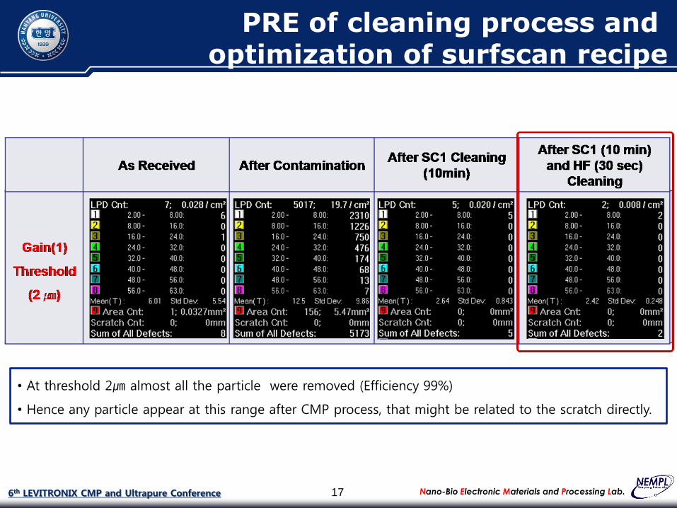
PRE of cleaning process and optimization of surfscan recipe
Gain(1)
Threshold
(2 ㎛)
• At threshold 2㎛ almost all the particle were removed (Efficiency 99%)
• Hence any particle appear at this range after CMP process, that might be related to the scratch directly.

18 6th LEVITRONIX CMP and Ultrapure Conference Nano-Bio Electronic Materials and Processing Lab.
CMP Performance & Scratch Number (Reference)
Removal Rate & Non-uniformity
• Evaluation of Reference process during 360 times CMP
- Process Condition : 4.5 psi, head 67rpm/ platen 73 rpm, 30s
- RR : Avg. 460 nm/min, WIWNU : below 5%
• Evaluation of Reference Scratch formation during 360 times CMP
- Reference scratch formation : below 15EA
0 50 100 150 200 250 300 350 4000
100
200
300
400
500
600
0 50 100 150 200 250 300 350 4000
5
10
15
20
Rem
oval
Rate
(n
m/m
in)
The time of CMP
Removal Rate
No
n-U
nifo
rmity
(%)
Non-uniformity
-50 0 50 100 150 200 250 300 350 400
0
30
60
90
120
150
Th
e n
um
ber
of
scra
tch
(E
A)
The time of CMP
2 ~ 63 m
Scratch Number (reference)
Control the high scratch using the break-in process
- 30min with DIW - 10 min with slurry

19 6th LEVITRONIX CMP and Ultrapure Conference Nano-Bio Electronic Materials and Processing Lab.
Scratch Detection Mathods
(0,0)
Surface Analyzer Image Section Paper
• The surface analyzer image exactly overlapped with section paper to detect the location of the defects
• Each individual defect was inspected by Optical Microscope using the above approach
(0,0)
Both surface analyzer image and
section paper exactly overlapped

20 6th LEVITRONIX CMP and Ultrapure Conference Nano-Bio Electronic Materials and Processing Lab.
CMP
Clean
Oxide Wafer
Post-CMP Cleaning
Scratch Image
By Optical Microscope ( LV-
100D, Nikon, Japan)
• Lap Scale (micron)
• Specific Scratch
at Specific Area
• Scratch Characterization
( Dimension, Shape)
≤ 15000 ea
≤ 20 ea
SC-1
(600C, 10min)
DHF
(0.5vol%,
210s)
Marangoni
IPA Dry
Removal of Slurry Reside
Extension of Scratch
Removal of Water Mark
By Surface Particle Scanner
(surfscan 6200 KLA, Tencor, USA)
Summary of Scratch Detection Method
SC-1
(600C, 10min)
Removal of
Re-contamination particle

21 6th LEVITRONIX CMP and Ultrapure Conference Nano-Bio Electronic Materials and Processing Lab.
Capturing the image of a scratch by the new method
• The specific scratch at specific region could be observed by a microscope using wafer matching method.
• Over 95% accuracy was observed in detecting the scratches
• And also, the scratch analysis was done by AFM
Wafer Matching Test after CMP
5.664 um
5.317 um
OM image
AFM image

22 6th LEVITRONIX CMP and Ultrapure Conference Nano-Bio Electronic Materials and Processing Lab.
Classification of Scratches Formed on Oxide Surface
Line chatter Broken chatter Group chatter
• The Major type of scratch shapes are Chatter on oxide surface : Chatter type occupies more than 70%
Continuous Line Broken Line Random
•Sliding of embedded large particle • Indentation depth determine the scratch shape
• Irregular scratch source and it’s behavior may generate the random type

23 Nano-Bio Electronic Materials and Processing Lab. 6th LEVITRONIX CMP and Ultrapure Conference
Scratch Formation Theory (Chatter Scratch Formation)
* H-J Kim, et al., “Modeling on the CMP Scratch”, 43th Technical Meeting of Korea CMPUGM (2009)
• Stick-Slip phenomena
- Stick friction is increased by the stress concentration,
which induce the Scratch formation
- Slip friction is generated after surface fracture, which
decide the distance between chatter scratch
Most probable mechanism

24 6th LEVITRONIX CMP and Ultrapure Conference Nano-Bio Electronic Materials and Processing Lab.
Vacuum
Pump
Slurry Delivery Atomizer
Head
Conditioner
After CMP
• To investigate the scratch sources generated during polishing, a gathering system was developed to collect the byproducts directly during the CMP process. • After examining the several locations , to gather byproducts, it was found that gathering of byproducts at the back position of the wafer would be the better position .
Gathering of CMP byproducts
Schematic diagram of slurry gathering system

25 6th LEVITRONIX CMP and Ultrapure Conference Nano-Bio Electronic Materials and Processing Lab.
• The comparison was performed among fresh pad and byproducts collected during just conditioning and actual polishing
• SEM images shows the presence of some large matter in byproducts
• EDX analysis confirms that the large matters related to pad debris. The byproducts of polishing also contains Si composition,
which is due to the slurry
• It could be concluded that generation of pad debris is significant during CMP process and their effect should be studied.
SEM and EDX analysis of gathered CMP byproducts

26 6th LEVITRONIX CMP and Ultrapure Conference Nano-Bio Electronic Materials and Processing Lab.
The number of Byproduct after CMP
5 10 15 20 25 30
0
500
1000
1500
2000
2500
3000
3500
4000
Slurry 100L
Nu
mb
er
of
Part
icle
Particle Size (m)
Fresh slurry
In-situ conditioning
• After CMP process, large particle number is increased in byproduct (byproduct 100 uL) • During in-situ conditioning, Pad debris is generated which affect to scratch formation
Number of Byproduct

27 6th LEVITRONIX CMP and Ultrapure Conference Nano-Bio Electronic Materials and Processing Lab.
0
20
40
60
80
100
Sc
ratc
h N
um
be
r (%
)
Addition of Pad Debris
Rolli
ng type
Total L
ine
Bro
ken L
ine
Contin
uous Lin
e
Total C
hatte
r
Gro
up Chat
ter
Dot C
hatte
r
Bro
ken C
hatte
r
Line
Chat
ter
Correlation between scratch source and scratch shape
0
20
40
60
80
100
Rolli
ng type
Total L
ine
Bro
ken L
ine
Contin
uous Lin
e
Total C
hatte
r
Gro
up Chat
ter
Dot C
hatte
r
Bro
ken C
hatte
r
Line
Chat
ter
Scra
tch
Nu
mb
er
(%) Reference Wafer
0
20
40
60
80
100
Sc
ratc
h N
um
be
r (%
)
Addition of Dried Slurry Particles
Rolli
ng type
Total L
ine
Bro
ken L
ine
Contin
uous Lin
e
Total C
hatte
r
Gro
up Chat
ter
Dot C
hatte
r
Bro
ken C
hatte
r
Line
Chat
ter 0
20
40
60
80
100
Sc
ratc
h N
um
be
r (%
)
Addition of Diamond Particles
Rol
ling
type
Tota
l Lin
e
Bro
ken
Line
Con
tinuo
us L
ine
Tota
l Cha
tter
Gro
up C
hatter
Dot
Cha
tter
Bro
ken
Cha
tter
Line
Cha
tter
• Different scratch sources added individually to the CMP process and then their effect on scratch shapes was studied
28 6th LEVITRONIX CMP and Ultrapure Conference Nano-Bio Electronic Materials and Processing Lab.
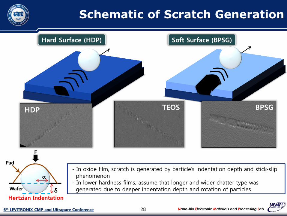
δ
α
Pad
F
Wafer
Hertzian Indentation
Schematic of Scratch Generation
Hard Surface (HDP) Soft Surface (BPSG)
- In oxide film, scratch is generated by particle’s indentation depth and stick-slip phenomenon
- In lower hardness films, assume that longer and wider chatter type was generated due to deeper indentation depth and rotation of particles.
HDP TEOS BPSG
29 6th LEVITRONIX CMP and Ultrapure Conference Nano-Bio Electronic Materials and Processing Lab.
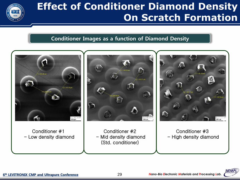
Conditioner #1 - Low density diamond
Conditioner #2 - Mid density diamond
(Std. conditioner)
Conditioner #3 - High density diamond
Effect of Conditioner Diamond Density On Scratch Formation
Conditioner Images as a function of Diamond Density

30 6th LEVITRONIX CMP and Ultrapure Conference Nano-Bio Electronic Materials and Processing Lab.
• In high density conditioner case, Lower RR (450 nm/min) is measured than that of other conditioners
• Conditioning with DIW
- Larger pad particle is generated during high density diamond conditioning
0
1
2
3
4
5
300
350
400
450
500
550
No
n-u
nifo
rmity
(%)
Rem
oval R
ate
(n
m/m
in)
Removal Rate
HighMidLow
Diamond Density
Non-uniformity
Removal Rate & Non-uniformity
CMP Performance as a function of Diamond Density
After conditioning with DIW
10 100 1000 10000 100000 10000000
10
20
30
40
50
60
Low
Mid
High
Dif
fere
nti
al n
um
be
r %
Diameter (nm)
Diamond Density

31 6th LEVITRONIX CMP and Ultrapure Conference Nano-Bio Electronic Materials and Processing Lab.
- Pad height probability is measured after conditioning - (Wyco-NT9100, VEECO, USA)
row
mid
high
• After conditioning using the High density diamond conditioning, Pad height probability is generated at high pad height • It means that conditioning is provided to only pad asperity area. Also, enough conditioning isn’t provided at the pore area • Because the pressure on each diamond of high density is lower than that of standard or low density conditioner
Pad height probability(Data for *Dow chemical Company)
Polishing Pad
Diamond conditioner
Pad Surface Analysis after conditioning

32 6th LEVITRONIX CMP and Ultrapure Conference Nano-Bio Electronic Materials and Processing Lab.
- The scratch number is measured after HF 0.5 vol% etching (210s)
- The highest number of scratch is generated during polishing with high density diamond
conditioner
- The scratch number may be affected by conditioner performance and generated Pad particle size
Scratch Number as a function of Diamond Density
0
10
20
30
40
50
60
70
3
3
3
2
2
2
1
1
HF 0.5% etching (210s)
1
High DensityMid Density
Th
e N
um
be
r o
f S
cra
tch
(E
A)
Low Density

33 6th LEVITRONIX CMP and Ultrapure Conference Nano-Bio Electronic Materials and Processing Lab.
Summary
Optimized Post CMP Cleaning Process
- Cleaning sequence : SC1 (10min) HF Cleaning (210s) SC1 (10min) wafer Dry
SC1 Cleaning : Removal of particles
HF Cleaning : Removal of particles and extension of scratches
Classification and sub classification of scratch shapes on oxide after CMP
- The major type of scratch shapes are Chatter on oxide surface
- Also, unstable friction between pad and wafer may generate the Broken/Group chatter scratches
Scratch Source Vs Scratch Shape
- Three different scratch sources were tested on the shape of scratch formation.
- It was found that specific scratch source has specific effect on scratch shape and size.
- The dried and diamond particles showed severe effect on scratch formation due to their hard nature
Characterization of Process Consumables
- Surface hardness : Indentation depth by abrasive particle affect to scratch number and shape
- LPC : Large particle of slurry can cause the unstable scratch formation
- Conditioner : Conditioner performance may affect to the pad debris generation and scratch formation

34 6th LEVITRONIX CMP and Ultrapure Conference Nano-Bio Electronic Materials and Processing Lab.