Embed Size (px)
Citation preview

CMOS Mixed Signal Design
CMOS Mixed Signal DesignPart I: OpAmp Design
Dinesh Sharma
Microelectronics Group, EE DepartmentIIT Bombay, Mumbai
September 19, 2010

CMOS Mixed Signal Design
Introduction
Linear Mode
Linear Mode of Operation
V
V
V V
OH
OL
iL iH
Inverter Transfer Curve
Analog circuits require theoutput voltage to be sensitiveto the input voltage.
Digital logic requires theoutput to be insensitive to theexact input voltage.
Circuits need to be biased for operation in the linear regime.
CMOS Mixed Signal Design
Single Transistor Amplifier
A Single Transistor Amplifier
v
vo
Vd
Id
i Vg
dId =∂Id∂Vg
dVg +∂Id∂Vd
dVd
∂Id∂Vg
= gm (Transconductance)
∂Id∂Vd
= go (O/P conductance)
The current source load keeps the drain current constant. So
dId = 0 = gmvi + govo
Hence, the voltage gain (Ao) is
Ao =vo
vi= −
gm
go= −gmro

CMOS Mixed Signal Design
Single Transistor Amplifier
Transistor Characteristics
Transistor Characteristics
gm and go depend on the transistor characteristics.In saturation,
Id ≃K2
(Vgs − VT )2
where, K is the conductivity factor given by:
K = K ′
(
WL
)
≡ µCox
(
WL
)
VT is the threshold voltageW and L are transistor width and length respectively.µ is the mobilityand Coxis the gate oxide capacitance per unit area.

CMOS Mixed Signal Design
Single Transistor Amplifier
Transistor Characteristics
Transconductance
Let VGT ≡ (Vgs − VT )
Then Id =KV 2
GT
2and VGT =
√
2IdK
gm =∂Id∂Vg
= KVGT = K ′
(
WL
)
VGT
Also gm = KVGT = K
√
2IdK
=√
2KId =
√
2K ′
(
WL
)
Id
Similarly, K =2Id
VGT2 ; Therefore gm =
2IdVGT
2 VGT =2IdVGT

CMOS Mixed Signal Design
Single Transistor Amplifier
Transistor Characteristics
Which formula?
gm = K ′
(
WL
)
VGT
gm =
√
2K ′
(
WL
)
Id
gm =2IdVGT
To increase gm
should we increase VGT ?or decrease it?Is gm linearly dependent ontransistor size?dependent on its square root?or is it independent of transistorsize?
In fact, which formula should be applied depends on how thetransistor is biased and sized. If size and VGT are known, thefirst formula applies. If the drain current and size are known, thesecond one does. If gate voltage and drain current are givenand the transistor is accordingly sized, the third formula shouldbe used.

CMOS Mixed Signal Design
Single Transistor Amplifier
Transistor Characteristics
Output conductance
Assuming a simple Early effect like model, we can write for go:
go ≃ λ′Id/L
where L is the channel length and λ is a technology dependentparameter. In terms of geometry and VGT , we can write:
go =λ′K ′
2WL2 V 2
GT
The Early Voltage VA is L/λ′. So,
go ≃ Id/VA =K ′W2λ′
(
VGT
VA
)2

CMOS Mixed Signal Design
Single Transistor Amplifier
DC Voltage Gain
Voltage Gain
The voltage gain in terms of geometry and VGT :
Ao =2L
λ′VGT
In terms of drain current and geometry:
Ao =1λ′
√
2K ′WLId
Thus, if the transistor is biased at constant current, the DC gainis determined by the square root of the gate area.
CMOS Mixed Signal Design
Single Transistor Amplifier
AC Behaviour
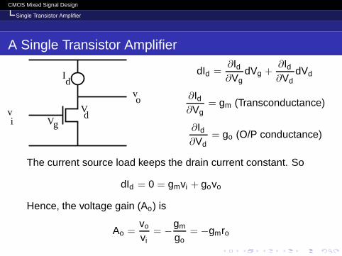
AC Behaviour
G
S
D
S
vi
vo
Cg
Cgd
gm vi ro Co
sCgd (vi − vo) − gmvi −vo
ro− sCovo = 0
vi(
sCgd − gm)
− vo
(
sCgd +1ro
+ sCo
)
= 0
So the AC gain A1 =vo
vi= −gmro
1 − sCgd/gm
1 + sro(cgd + co)

CMOS Mixed Signal Design
Single Transistor Amplifier
AC Behaviour
Bandwidth
A1 = −gmro1 − sCgd/gm
1 + sro(cgd + co)
Let Ctot ≡ Cgd + Co
Then, A1 = Ao1 − sCgd/gm
1 + sroCtot
Normally, ωCgd/gm << 1
Therefore, A1 ≃Ao
1 + sroCtot
This describes the frequency response of a system with onedominant pole. The bandwidth is given by 1/roCtot .

CMOS Mixed Signal Design
Single Transistor Amplifier
AC Behaviour
Gain Bandwidth Product
BW GBW
Gai
n (d
b)
oA
oA - 3db
0 db
Frequency
GBW = gmro ·1
roCtot=
gm
Ctot
The gain bandwidth product (or the cutoff frequency) isindependent of ro.

CMOS Mixed Signal Design
Single Transistor Amplifier
AC Behaviour
Maximum GBW
GBW is max. when there is no load connected and the load isentirely due to the device capacitance itself. Then the loadcapacitance is proportional to the device width.
Ctot = χW where χ is a technological parameter.
GBWmax =gm
χW
GBWmax =K ′VGT
χL
=1χ
√
2K ′IdWL
=2Id
χWVGT
CMOS Mixed Signal Design
Single Transistor Amplifier
AC Behaviour
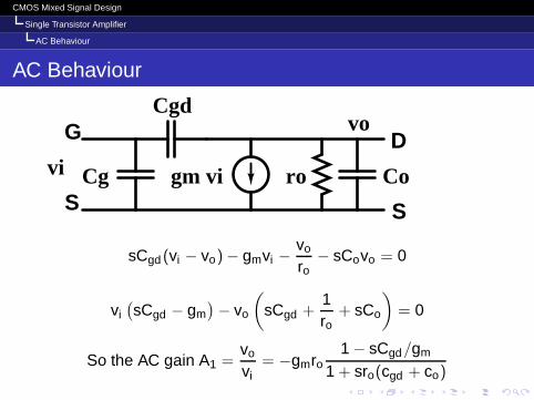
Summary
Free Design Variables:Parameters W , L, VGT W , L, Id L, VGT , Id
gm K ′WL VGT
√
2K ′ WL Id
2IdVGT
goλ′K ′WV 2
GT2L2
λ′IdL
λ′IdL
Ao2L
λ′VGT
1λ′
√
2K ′WLId
2Lλ′VGT
GBW K ′WVGTLCtot
√
2K ′WIdL
1Ctot
2IdVGT Ctot
GBW maxK ′VGT
χL1χ
√
2K ′IdWL
K ′VGTχL

CMOS Mixed Signal Design
Single Transistor Amplifier
AC Behaviour
Technological Constraint
Ao · GBWmax =2L
λ′VGT·
K ′VGT
χL=
1λ′
√
2K ′WLId
·1χ
√
2K ′IdWL
So Ao · GBWmax =2K ′
λ′χ
Therefore, this quantity is a technological constant and thedesigner has no control over it.What if an application requires a Gain-GBW product higherthan this value?

CMOS Mixed Signal Design
Cascode Amplifier
Cascode Amplifier
Id
V
Vd1
d2
M1
M2
V
V
v
v
g1
g2
in
outV
ref
dId = gmeqdVg1 + goeqdVd2
So gmeq =∂Id
∂Vg1with dVd2 = 0
and goeq =∂Id
∂Vd2with dVg1 = 0
To calculate gmeq, we put a voltage source atthe output node and calculate ∂Id
∂Vg1.
goeq is calculated by putting a voltage source atvg1 and calculating ∂Id
∂Vd2.

CMOS Mixed Signal Design
Cascode Amplifier
Cascode eq. gm
Equivalent gm of Cascode
Id
V
Vd1
d2
M1
M2
V
V
v
v
g1
g2
in
outV
ref
gmeq =∂Id
∂Vg1with dVd2 = 0
dVds2 = −dVd1 , dVgs2 = −dVd1
id = gm1vg1 + go1vd1
id = −gm2vd1 − go2vd1
So vd1 = −id
gm2 + go2
id = gm1vg1 − idgo1
gm2 + go2
gmeq =id
vg1= gm1
gm2 + go2
go1 + go2 + gm2≃ gm1

CMOS Mixed Signal Design
Cascode Amplifier
Cascode eq. go
Equivalent go of Cascode
goeq =∂Id
∂Vd2with dVg1 = 0
dVgs1 = 0, dVgs2 = −dVd1, dVds2 = dVd2 − dVd1
Id
V
Vd1
d2
M1
M2
V
V
v
v
g1
g2
in
outV
ref
id = 0 + go1vd1, sovd1 =id
go1
id = −gm2vd1 + go2(vd2 − vd1)
id = −idgm2 + go2
go1+ go2vd2
goeq =id
vd2=
go1go2
go1 + go2 + gm2
goeq ≃ go1go2
gm2

CMOS Mixed Signal Design
Cascode Amplifier
DC gain of Cascode
DC gain of Cascode
Ao = −gmeq
goeq= −
gm1(gm2 + go2)
g01 + g02 + gm2·
g01 + g02 + gm2
g01g02
So Ao = −gm1(gm2 + go2)
g01g02= −
gm1
g01·
(
1 +gm2
g02
)
Let A01 ≡ −gm1
g01common source gain
And A02 ≡ 1 +gm2
g02common gate gain
Then, Ao = −A01 · A02
DC gain = the product of the DC gain of the two transistors.

CMOS Mixed Signal Design
Cascode Amplifier
AC Behaviour of Cascode
AC Behaviour of Cascode
Id
V
Vd1
d2
M1
M2
V
V
v
v
g1
g2
in
outV
refG
S
vi
vo
CoCg1
Cdg1
gm1 viro1
vx
ro2
gm2 vx
We shall see presently that vx is quite small.
Initially, we shall ignore the effect of the drain capacitance ofthe lower transistor and the gate capacitance of the upper one.If necessary, we can always replace ro1 by ro1‖Cds1‖Cg2.

CMOS Mixed Signal Design
Cascode Amplifier
AC Behaviour of Cascode
G
S
vi
vo
CoCg1
Cdg1
gm1 viro1
vx
ro2
gm2 vx
gm2vx +vx − vo
ro2= sCovo
vx =1 + sro2Co
1 + gm2ro2vo =
1 + sro2Co
A2vo
Since A2 is quite large, vx is very small compared to vo.

CMOS Mixed Signal Design
Cascode Amplifier
AC Behaviour of Cascode
G
S
vi
vo
CoCg1
Cdg1
gm1 viro1
vx
ro2
gm2 vx
sCdg1(vi − vx ) = gm1vx +vx
ro1+ sCovo
vo
vi= −
(A1 − sro1Cdg)A2
(1 + sro2Co)(1 + sro1Cdg) + A2sCoro1
If sro1Cdg is small,
Voltage gain =vo
vi= −
A1A2
1 + sro1Co(A2 + ro2/ro1)
This shows that the DC gain is multiplied by A2 and thebandwidth is reduced by roughly the same factor.

CMOS Mixed Signal Design
Cascode Amplifier
AC Behaviour of Cascode
Example Cascode Design
We want to design a cascode amplifier with the followingspecifications:
DC gain = 2500
Gain-Bandwidth product = 100MHz.
Load capacitance = 1 pF
Id
V
Vd1
d2
M1
M2
V
V
v
v
g1
g2
in
outV
ref
The two transistors in cascodeconfiguration have identical geometriesand the load is an ideal current source.Assume the following technologicalparameters:K ′
n = 150µA/V 2, VTn = 0.5V , VE = 20VAssume the supply voltage to be 3.3V.

CMOS Mixed Signal Design
Cascode Amplifier
AC Behaviour of Cascode
Calculation of gm
The gain bandwidth product is given by gmC . So,
2π × 108 =gm
C=
gm1
10−12
So gm1 = 628.3µS
Since the same current flows through the two transistors andthey have the same geometry, gm1 = gm2, go1 = go2.
Let A =gm1
go1=
gm2
go2
Therefore,
2500 =gm1
go1·
(
1 +gm2
go2
)
= A(A + 1)
This gives A ≃ 49.5.

CMOS Mixed Signal Design
Cascode Amplifier
AC Behaviour of Cascode
Calculation of bias current and geometry
49.5 =628.3 × 10⁻⁶
go1so go1 = 12.7µS
Therefore go1 = 12.7 × 10−6 =IdVE
=Id20
From where, the drain current is 254µA.
Since gm1 =
√
2K ′WL
Id ,WL
=628.32 × 10⁻¹²
300 × 10−6 × 254 × 10−6 ≃ 5.2
Therefore gm = 628.3µS,WL
= 5.2, Id = 254µA
CMOS Mixed Signal Design
Cascode Amplifier
AC Behaviour of Cascode
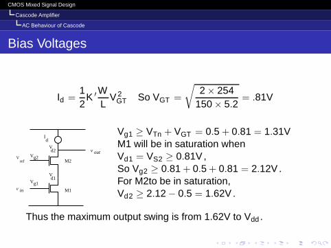
Bias Voltages
Id =12
K ′WL
V 2GT So VGT =
√
2 × 254150 × 5.2
= .81V
Id
V
Vd1
d2
M1
M2
V
V
v
v
g1
g2
in
outV
ref
Vg1 ≥ VTn + VGT = 0.5 + 0.81 = 1.31VM1 will be in saturation whenVd1 = VS2 ≥ 0.81V ,So Vg2 ≥ 0.81 + 0.5 + 0.81 = 2.12V .For M2to be in saturation,Vd2 ≥ 2.12 − 0.5 = 1.62V .
Thus the maximum output swing is from 1.62V to Vdd .

CMOS Mixed Signal Design
Cascode Amplifier
AC Behaviour of Cascode
DC level incompatibility
The output DC level of a cascode amplifier is higher than theinput DC level. This causes problems with direct connection tothe next stage, or with DC feed back to itself.
These problems can be reduced if we usea complementary arrangement of n and pchannel transistors for cascoding.
The upper transistor of the cascodearrangement can be thought of as asource follower to its bias voltage, whichkeeps the drain voltage of the loweramplifier transistor (nearly) constant.
Can we use a p channel transistor as asource follower?
Vout
Vbiasn
Vin
LoadVdd
Gnd

CMOS Mixed Signal Design
Cascode Amplifier
AC Behaviour of Cascode
Alternative Cascode
The p source follower will keep the drainvoltage of the amplifier at ≃ Vbiasp + |VTp|,allowing the cascode action as before.
Unfortunately, the circuit won’t work asthere is no path between Vdd and ground!
We can rectify this problem by providing acurrent source p load to the amplifiertransistor M1.
Vbiasp
LoadGnd
Vdd
Vout
M1M2

CMOS Mixed Signal Design
Cascode Amplifier
Folded Cascode
Folded Cascode
M1
M2
M3
Vin
Vbiasp1Vdd
GndLoad
Vbiasp2
Vout
This arrangement is called a folded cascode.M3 provides the bias current.M2 and M3 keep the drain voltage of M1 nearlyfixedId3 - Id1 flows through the p channelcascoding transistor M2, which providesamplification in a common gate configuration.
rout = (1 + gm2ro2)(ro1||ro3) + ro2
This is lower than the output resistance of the telescopiccascode stage, because of the paralleling of ro1 and ro3.
However, it is much higher than the single transistor outputresistance.

CMOS Mixed Signal Design
Current Mirrors
Current Source Loads
Up to now we have assumed current source loads. How do weimplement these?
A transistor in saturation has a (nearly) constant draincurrent.
Therefore single transistors (preferably with long channels)can be used as current sources/sinks.
These act as current sources/sinks only over some voltagerange — not for all voltages.
There is a weak dependence on voltage due to nonzerooutput conductance.
This dependence can be reduced by using a cascodestage.

CMOS Mixed Signal Design
Current Mirrors
A simple Current Mirror
M1 M2
Iref Io
Vref
For M1, Vds = Vgs > Vgs − VT
Therefore M1 is saturated.
Iref =K2
(Vref − VT )2
Therefore Vref = VT +
√
2Iref
K
If M2 is also saturated, Io = Iref
Thus M2 can act as a current source load
if Vo > Vref − VT i.e. Vo >
√
2Iref
K

CMOS Mixed Signal Design
Current Mirrors
Load for a Cascode stage
Vbiasp1
Vbiasp2
Vbiasn
Vin
Vout
Vdd
Gnd
The output resistance of the load appears inparallel with that of the amplifying stage.If we use a single transistor current load for acascode, the output resistance of the load willbe ≈ ro while that of the cascode stage will be≈ A × ro.The effective output resistance will thus bedominated by the much lower resistance of theload and we shall lose the advantages of thecascode stage.It is important, therefore, that the load alsoshould be a current source made from acascode pair.

CMOS Mixed Signal Design
Current Mirrors
A cascode current mirrorIref Io
VrefM1 M2
M3Vb
Vx Vy
A single transistor current mirror will havesome dependence on the drain voltagedue to its output resistance.This dependence can be reducedsubstantially by using a cascode stage.However, this reduces the availablevoltage range over which the transistorsare saturated.
For saturation of M2 Vy ≥ Vref − VT =
√
2Iref
K
Therefore Vb ≥ 2
√
2Iref
K+ VT
For saturation of M3 Vo ≥ 2
√
2Iref
K

CMOS Mixed Signal Design
Current Mirrors
Self biased Cascode current mirror
Iref
VrefM1 M2
M3
Vb
Vx Vy
Io
M0
This circuit does not need an externalvoltage bias.
The reference side of the mirror generatesthe bias voltages for both the transistors ofthe cascode output side.
However, this reduces the voltage rangeover which the the output may swing.
Vb = 2
√
2Iref
K+ 2VT
For saturation of M3 Vo ≥ 2
√
2Iref
K+ VT
The output voltage needs to be a VT higher than the minimum.

CMOS Mixed Signal Design
Current Mirrors
Folded Cascode with load
M1
M2
M3
Vin
Gnd
Vbiasp1
Vbiasp2
Vout
Vbiasn2
Vbiasn1
Vdd
The load for the folded cascode should also bea cascode pair.Here two n channel transistors in cascodeconfiguration are used as the load.
One major advantage of the folded cascode is that the outputcan be directly coupled to the input for negative feedback.

CMOS Mixed Signal Design
Current Mirrors
Folded Cascode with Load
M1
M2
M3
Vin
Gnd
Vbiasp1
Vbiasp2
Vout
Vbiasn2
Vbiasn1
Vdd
The single transistor amplifier can be replaced by anytransconductance, of course. In operational amplifiers, the
single transistor stage will be replaced by a differential amplifier.

CMOS Mixed Signal Design
Operational Amplifiers
Differential Amplifiers
Differential Amplifiers
Circuits which amplify the difference of two input voltages (eachof which has equal and opposite signal excursions) have manyadvantages over single ended amplifiers.
Noise picked up by both inputs gets canceled in the output.
Input and feedback paths can be isolated.
If both inputs have the same DC bias, the output isinsensitive to changes in the bias.
CMOS Mixed Signal Design
Operational Amplifiers
Differential Amplifiers
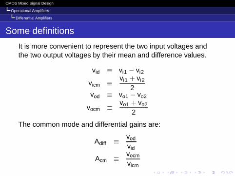
Some definitions
It is more convenient to represent the two input voltages andthe two output voltages by their mean and difference values.
vid ≡ vi1 − vi2
vicm ≡vi1 + vi2
2vod ≡ vo1 − vo2
vocm ≡vo1 + vo2
2
The common mode and differential gains are:
Adiff ≡vod
vid
Acm ≡vocm
vicm

CMOS Mixed Signal Design
Operational Amplifiers
Differential Amplifiers
Common Mode Rejection Ratio
For a good diff amp, the differential gain should be high andindependent of input common mode voltage, whereas thecommon mode gain should be as low as possible. Thecommon mode rejection ratio is:
CMRR ≡ 20 logAdiff
AcmdB

CMOS Mixed Signal Design
Operational Amplifiers
Differential Amplifiers
Will this do?
vi 1 vi 2
vo 1 vo 2
Vdd
One (not very good) way of implementing a diff amp is to usetwo single ended amplifiers as shown above.
Output = Vo1 − Vo2
Here the transistor currents, and hence the differential gain, willdepend on the common mode voltage. This is not desirable aswe would like the circuit to ignore the common mode voltageand to amplify just the difference signal.

CMOS Mixed Signal Design
Operational Amplifiers
Differential Amplifiers
The long tail pair
A better diff amp can be implemented by adding a currentsource to keep the total current constant.
vi 1 vi 2
vo 1 vo 2
Vdd
Is
Vs
If the common mode voltage appearing at thetwo inputs changes, it will only change thevoltage at the node where the two sources join(Vs). However, the current remains unchangeddue to the current source - and therefore, thedifferential gain is unaffected by the commonmode voltage.

CMOS Mixed Signal Design
Operational Amplifiers
Differential Amplifiers
Diff amp with single ended output
vi 1 vi 2
Vdd
Is
VsMn1 Mn2
Mp1 Mp2i out
iout = I(Mp2)− I(Mn2)
I(Mp2) = I(Mp1) (current mirror)I(Mp1) = I(Mn1) (series connection)
iout = I(Mn1) − I(Mn2) = gm(vi1 − vi2)
iout ≡ Gm(vi1 − vi2) = Gmvid
Thus we have a single output which is proportional to thedifference of inputs.The effective Gm is just the gmof either of the diff-pairtransistors.

CMOS Mixed Signal Design
Operational Amplifiers
Differential Amplifiers
Gain of the OTA
vi 1 vi 2
Vdd
Is
VsMn1 Mn2
Mp1 Mp2i out
This circuit is also called an operationaltransconductance amplifier (OTA) because theoutput is a current.
Rout = ro(Mn2)‖ro(Mp2)
So DC voltage gain = gm(ro(Mn2)‖ro(Mp2))
and GBW =gm
CL
CL includes Cdg and Cd for Mn2 and Mp2, as well as the loadcapacitance.

CMOS Mixed Signal Design
Operational Amplifiers
The two stage op-amp
Two stage op-amp
vi 1 vi 2
Vdd
VsMn1 Mn2
Mp1 Mp2i out
VbiasMn3
Mp3
Mn4
vout
A simple two stage op-amp can be constructedby following the diff amp by a common sourcestage with a constant current load.The current source for the diff amp isimplemented by an n channel MOS transistorin saturation.
The two stage design permits us to optimize the output stagefor driving the load and the input stage for providing gooddifferential gain and CMRR.A diff amp with n transistors and an output stage with p driver isshown. However, a p type diff amp with n type common sourcestage is better for low noise operation.

CMOS Mixed Signal Design
Operational Amplifiers
The two stage op-amp
op-amp eq. circuit
gm11 v1 gm22 v2
R1 R2C1 C2
v2 v0
Differential Stage Output Stage
Each stage of the opamp can be considered a gain stage with asingle pole frequency response.Notice that the phase of the output of each stage will undergo aphase change of 90o around its pole frequency.

CMOS Mixed Signal Design
Operational Amplifiers
The two stage op-amp
op-amp Compensation
Most opamps are used with negative feedback.If the opamp stages themselves contribute a phase differenceof 180o, the negative feedback will appear as positive feedback.If the gain at this frequency is > 1, the circuit will becomeunstable.Both stages of the opamp have a single pole frequencyresponse.The poles for both the stages can be quite close together.As a result, they can contribute a total of 180o phase shift overa relatively narrow frequency range.

CMOS Mixed Signal Design
Operational Amplifiers
The two stage op-amp
Pole Splitting
To avoid instability, we would like to arrange things suchthat the gain drops to below one by the time the phase shiftthrough the opamp becomes 180o.- Even if it means that we have to reduce the bandwidth ofthe op amp.
This is often achieved by a technique called pole splitting.
The lower frequency pole is brought to a low enoughfrequency, so that the gain diminishes to below one by thetime the second pole is reached.
One way of doing this is to use a Miller capacitor.

CMOS Mixed Signal Design
Operational Amplifiers
The two stage op-amp
Eq. Circuit of compensated Opamp
gm11 v1 gm22 v2
R1 R2C1 C2
v2 v0
Differential Stage Output StageCc
CMOS Mixed Signal Design
Operational Amplifiers
The two stage op-amp
Miller Compensation
C
A1 A2
The diff amp stage sees a load capacitance A 2C.This brings its pole to 1
ro1A2C .The total DC gain is A1A2.The bandwidth is set by the diff amp stage.
Therefore the gain-bandwidth product is:
A1A2
ro1A2C=
A1
ro1C

CMOS Mixed Signal Design
Operational Amplifiers
The two stage op-amp
Slew rate
Miller compensation also sets the slew rate of the op amp.
vi 1 vi 2
Vdd
VsMn1 Mn2
Mp1 Mp2i out
VbiasMn3
Mp3
Mn4
vout
For large signal input, the output current of theOTA = tail current.The effective load capacitance for this stage isA2 × C.
A2 × CdVdt
= I(Mn4)
Output of the OTA slews at a rate I(Mn4)A2×C .
So the op amp slews at a rate which is A2 times this value.
Hence the slew rate of the op amp is I(Mn4)C .

CMOS Mixed Signal Design
Operational Amplifiers
The two stage op-amp
Design Equations-I
vi 1 vi 2
Vdd
VsMn1 Mn2
Mp1 Mp2i out
VbiasMn3
Mp3
Mn4
vout
All transistors must be saturated
I(Mn1) = I(Mn2) =I(Mn4)
2I(Mn1) = I(Mp1) (Series connection)
I(Mp1) = I(MP2) (Mirror)
Mp1 is always saturated.Mp1, Mp2 have the same Vs, Vg, IdSince W/L(Mp2) = W/L(Mp1), MP2 will have the same Vd asMp1, and so, will be saturated.
CMOS Mixed Signal Design
Operational Amplifiers
The two stage op-amp
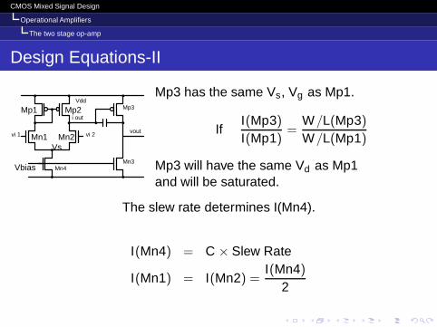
Design Equations-II
vi 1 vi 2
Vdd
VsMn1 Mn2
Mp1 Mp2i out
VbiasMn3
Mp3
Mn4
vout
Mp3 has the same Vs, Vg as Mp1.
IfI(Mp3)
I(Mp1)=
W/L(Mp3)
W/L(Mp1)
Mp3 will have the same Vd as Mp1and will be saturated.
The slew rate determines I(Mn4).
I(Mn4) = C × Slew Rate
I(Mn1) = I(Mn2) =I(Mn4)
2
CMOS Mixed Signal Design
Operational Amplifiers
The two stage op-amp
Design Equations-III
vi 1 vi 2
Vdd
VsMn1 Mn2
Mp1 Mp2i out
VbiasMn3
Mp3
Mn4
vout
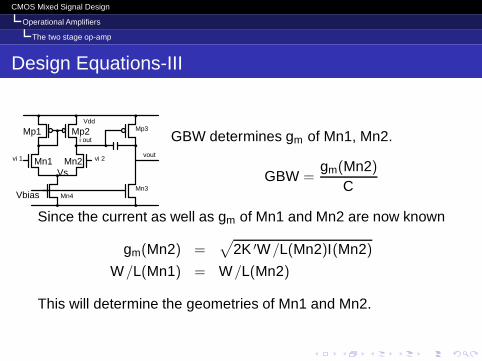
GBW determines gm of Mn1, Mn2.
GBW =gm(Mn2)
C
Since the current as well as gm of Mn1 and Mn2 are now known
gm(Mn2) =√
2K ′W/L(Mn2)I(Mn2)
W/L(Mn1) = W/L(Mn2)
This will determine the geometries of Mn1 and Mn2.

CMOS Mixed Signal Design
Operational Amplifiers
The two stage op-amp
Design Equations-IV
Currents through Mn2,Mp2, Mp3 and Mn3 are known
(go = Id/VA) where VA is the Early voltage = L/λ′
The overall DC gain is given by
A =gm(Mn2)gm(Mp3)
(go(Mn2)||go(Mp2))(go(Mp3)||go(Mn3))
As gmfor Mn2 and all govalues are known, this determines thegmfor MP3.Once we know the gmas well as the current for Mp3, we cancalculate its geometry.
CMOS Mixed Signal Design
Operational Amplifiers
The two stage op-amp
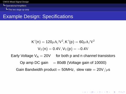
Example Design: Specifications
K ′(n) = 120µA/V2, K ′(p) = 60µA/V2
VT (n) = 0.4V, VT (p) = −0.4V
Early Voltage VA = 20V for both p and n channel transistors
Op amp DC gain = 80dB (Voltage gain of 10000)
Gain Bandwidth product = 50MHz, slew rate = 20V/µs

CMOS Mixed Signal Design
Operational Amplifiers
The two stage op-amp
Example Design-1
vi 1 vi 2
Vdd
VsMn1 Mn2
Mp1 Mp2i out
VbiasMn3
Mp3
Mn4
vout
We choose a compensation capacitor value of 2 pF.
We shall bias the second stage at 5 times the tail current ofthe differential stage.
From the slew rate, I(Mn4) = 2 × 10−12 × 2010−6 = 40µA
Therefore I(Mn1) = I(Mn2) = I(Mp1) = I(Mp2) = 20µAand I(Mp3) = I(Mn3) = = 200µA

CMOS Mixed Signal Design
Operational Amplifiers
The two stage op-amp
Example Design-2
vi 1 vi 2
Vdd
VsMn1 Mn2
Mp1 Mp2i out
VbiasMn3
Mp3
Mn4
vout
From the GBW requirement,
2π × 50 × 106 =gm(Mn2)
2 × 10⁻¹²
This gives gm(Mn2) ≃ 628µ℧.To get a gmof 628 µ℧ with a current of 20µA,
628 × 10−6 =√
2 × 120 × 10−6 × (W/L) × 20 × 10−6
this gives W/L(Mn2) ≈ 82 = W/L(Mn1)

CMOS Mixed Signal Design
Operational Amplifiers
The two stage op-amp
Example Design-3
vi 1 vi 2
Vdd
VsMn1 Mn2
Mp1 Mp2i out
VbiasMn3
Mp3
Mn4
vout
goof Mn2 and Mp2 = 20µA/20V = 1µ℧.Therefore go(Mn2)‖go(Mp2) = 2µ℧.goof Mn3 and Mp3 is = 200µA/20V = 10µ℧.Therefore go(Mp3)‖go(Mn3) = 20µ℧.
DC gain = 10000 =628µ℧
2µ℧×
gm(Mp3)
20µ℧
So, gm(Mp3) ≃ 637µ℧
CMOS Mixed Signal Design
Operational Amplifiers
The two stage op-amp
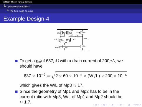
Example Design-4
vi 1 vi 2
Vdd
VsMn1 Mn2
Mp1 Mp2i out
VbiasMn3
Mp3
Mn4
vout
To get a gmof 637µ℧ with a drain current of 200µA, weshould have
637 × 10−6 =√
2 × 60 × 10−6 × (W/L) × 200 × 10−6
which gives the W/L of Mp3 ≈ 17.Since the geometry of Mp1 and Mp2 has to be in thecurrent ratio with Mp3, W/L of Mp1 and Mp2 should be≈ 1.7.

CMOS Mixed Signal Design
Operational Amplifiers
The two stage op-amp
Example Design-5
vi 1 vi 2
Vdd
VsMn1 Mn2
Mp1 Mp2i out
VbiasMn3
Mp3
Mn4
vout
Finally, we assume that an n type reference bias transistorof W/L = 4 is available with a current of 10 µA. This willgive the W/L of Mn4 and Mn3 as 16 and 80 respectively.
This completes the design for the simple two stage op amp.

CMOS Mixed Signal Design
Operational Amplifiers
Cascode Opamps
Telescopic Cascode Opamp
Vdd
Gnd
Vbiasp1Vbiasp2
Vbiasn2
Vbiasn1
Vout
Vin + Vin -
+
-
The telescopic cascode is a differential versionof the cascode amplifier discussed earlier.
Its gain is comparable to the two stage op-amp.
The output impedance is (very) high!
The output impedance in conjunction with theload capacitance constitutes the dominant poleof the system.

CMOS Mixed Signal Design
Operational Amplifiers
Cascode Opamps
Telescopic Cascode Opamp
Gain is comparable to the two stage opamp (product of twosingle stage amplifiers).
It needs a higher supply voltage compared to a two stageopamp.
The output stage is high impedance, so the dominant poleis at the output.
Compensation is provided by the load capacitance. So aminimum value of load capacitance is required for stability.
The output common mode voltage is different from theinput common mode voltage range.
This presents difficulties in direct coupling to the next stageand DC feedback to its own input.

CMOS Mixed Signal Design
Operational Amplifiers
Cascode Opamps
Folded Cascode
The common mode voltage incompatibility of a telescopiccascode can be solved by using a folded cascode.
-+
Vdd
Gnd
Vbiasp1
Vbiasp2
Vbiasn2
Vbiasn1
VoutVin + Vin -

CMOS Mixed Signal Design
Push Pull Output Stage
Push-Pull Op Amp
Differential to single ended conversion can be done in theoutput stage, by using a push-pull driver. The output loads inthe differential stage (Mp1 and Mp2) are diode connected.
Vdd
Gnd
Mp1 Mp2
Mn1 Mn2
Mn3 Mn4
Mp3
Vbias
vi- vi+
Mp4
Mn5
Vs
Out
Current through Mp2 is mirrored inthe output p transistor Mp4.
Current through Mp1 is mirrored intoa pMOS (Mp3) and passed througha diode connected nMOS (Mn3).
This current is mirrored in the outputstage nMOS (Mn4).
Mirroring ratio of Mp4 to Mp2 andMn4 to Mn3 should be identical (andcan be large).


![Ece-V-fundamentals of Cmos Vlsi [10ec56]-Solution](https://img.pdfslide.us/doc/110x75/55cf9d28550346d033ac77f4/ece-v-fundamentals-of-cmos-vlsi-10ec56-solution.jpg)

![Ece-V-fundamentals of Cmos Vlsi [10ec56]-Notes](https://img.pdfslide.us/doc/110x75/55cf9c56550346d033a97884/ece-v-fundamentals-of-cmos-vlsi-10ec56-notes-56310235399c2.jpg)