Embed Size (px)
Citation preview

EE1411
CMOS logicCMOS logic

EE1412
Properties of CMOS Gates SnapshotProperties of CMOS Gates SnapshotHigh noise margins:
VOH and VOL are at VDD and GND, respectively.
No static power consumption:There never exists a direct path between VDD and VSS (GND) in steady-state mode.
Comparable rise and fall times:(under appropriate sizing conditions)
Extremely high input resistance:nearly zero steady-state input current.
Always a path to Vdd or Gnd in steady state:low output impedance.

EE1413
Static CMOS CircuitStatic CMOS Circuit
- At every point in time (except during the switching transients) each gate output is connected to eitherVDD or Vss via a low-resistive path.
- The outputs of the gates assume at all times the value of the Boolean function, implemented by the circuit (ignoring, once again, the transient effects during switching periods).
- This is in contrast to the dynamic circuit class, which relies on temporary storage of signal values on the capacitance of high impedance circuit nodes.

EE1414
Static Complementary CMOSStatic Complementary CMOS
VDD
F(In1,In2,…InN)
In1In2
InN
In1In2InN
PUN
PDN
PMOS only
NMOS only
PUN and PDN are dual logic networks
……

EE1415
Threshold DropsThreshold DropsVDD
VDD → 0PDN
0 → VDD
CL
CL
PUN
VDD
0 → VDD - VTn
CL
VDD
VDD
VDD → |VTp|
CL
S
D S
D
VGS
S
SD
D
VGS

EE1416
NMOS Transistors NMOS Transistors in Series/Parallel Connectionin Series/Parallel Connection
Transistors can be thought as a switch controlled by its gate signal
NMOS switch closes when switch control input is high
X Y
A B
Y = X if A and B
X Y
A
B Y = X if A OR B
NMOS Transistors pass a “strong” 0 but a “weak” 1

EE1417
PMOS Transistors PMOS Transistors in Series/Parallel Connectionin Series/Parallel Connection
X Y
A B
Y = X if A AND B = A + B
X Y
A
B Y = X if A OR B = AB
PMOS Transistors pass a “strong” 1 but a “weak” 0
PMOS switch closes when switch control input is low

EE1418
Complementary CMOS Logic StyleComplementary CMOS Logic Style

EE1419
Example Gate: NANDExample Gate: NAND

EE14110
Example Gate: NORExample Gate: NOR

EE14111
Two-input CMOS NOR gate and reference inverter

EE14112
CMOS NOR Gate Truth Table and Transistor States
EE14113
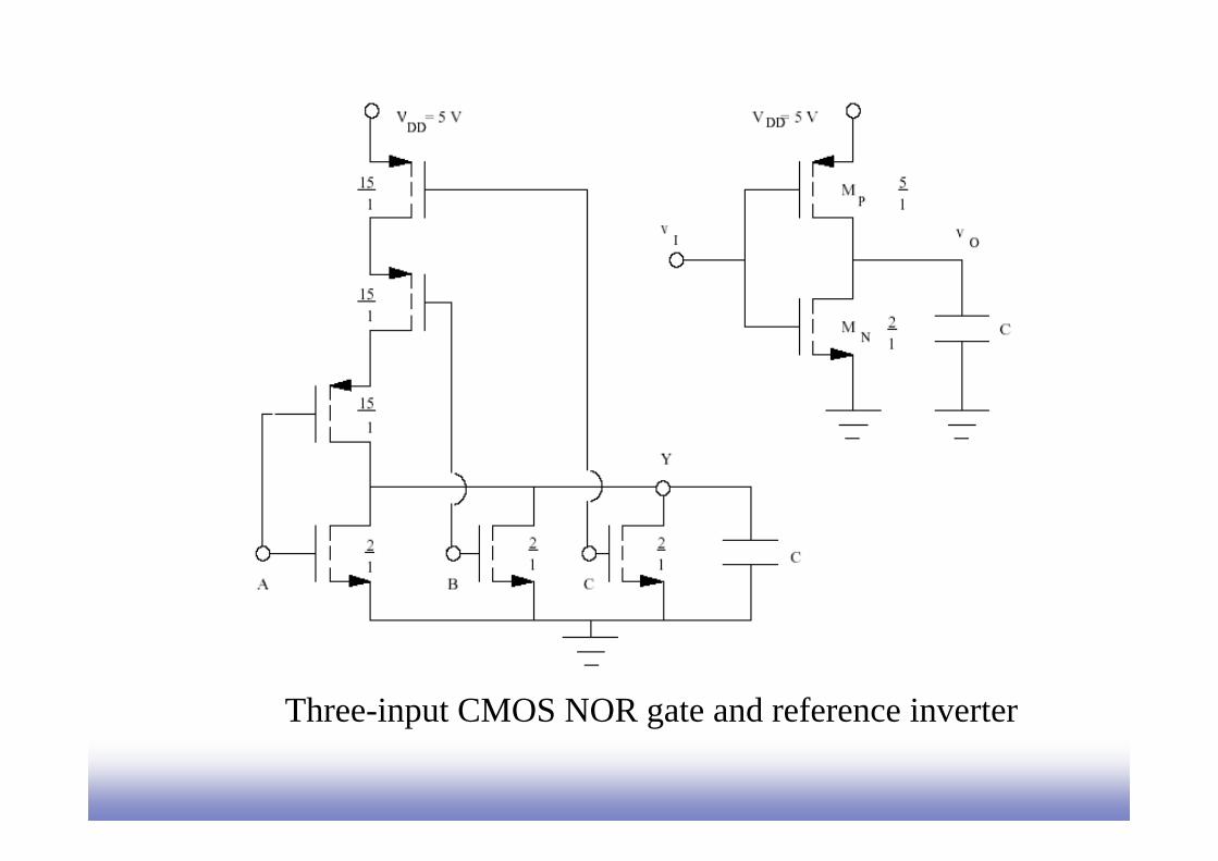
Three-input CMOS NOR gate and reference inverter

EE14114
Two-input CMOS NAND gate and reference inverter

EE14115
Switch Delay ModelSwitch Delay Model
A
Req
A
Rp
A
Rp
A
Rn CL
A
CL
B
Rn
A
Rp
B
Rp
A
Rn Cint
B
Rp
A
Rp
A
Rn
B
Rn CL
Cint
NAND2 INV NOR2

EE14116
Input Pattern Effects on DelayInput Pattern Effects on Delay
Delay is dependent on the pattern of inputsLow to high transition
both inputs go low– delay is 0.69 Rp/2 CL
one input goes low– delay is 0.69 Rp CL
High to low transitionboth inputs go high
– delay is 0.69 2Rn CL
CL
B
Rn
A
Rp
B
Rp
A
Rn Cint

EE14117
Delay Dependence on Input PatternsDelay Dependence on Input Patterns
-0,5
0
0,5
1
1,5
2
2,5
3
0 100 200 300 400
A=B=1→0
A=1, B=1→0
A=1 →0, B=1
time [ps]
Vol
tage
[V]
76A= 1→0, B=1
57A=1, B=1→0
35A=B=1→0
62A= 0→1, B=1
50A=1, B=0→1
69A=B=0→1
Delay(psec)
Input DataPattern
NMOS = 0.5μm/0.25 μmPMOS = 0.75μm/0.25 μmCL = 100 fF

EE14118
FanFan--In ConsiderationsIn Considerations
DCBA
D
C
B
A CL
C3
C2
C1
Distributed RC model(Elmore delay)
tpHL = 0.69 Reqn(C1+2C2+3C3+4CL)
Propagation delay deteriorates rapidly as a function of fan-in –quadratically in the worst case.
M1
M2
M3
M4

EE14119
ttpp of CMOS NAND as a functionof CMOS NAND as a functionof Fanof Fan--InIn
0
250
500
750
1000
1250
2 4 6 8 10 12 14 16
tpHL
quadratic
lineartpLH
t p(p
sec)
fan-in
Gates with a fan-in greater than 4 should be avoided.
tp

EE14120
ttpp as a Function of Fanas a Function of Fan--OutOut
2 4 6 8 10 12 14 16
tpNOR2
t p(p
sec)
eff. fan-out
All gates have the same drive current.
tpNAND2
tpINV
Slope is a function of “driving strength”
EE14121
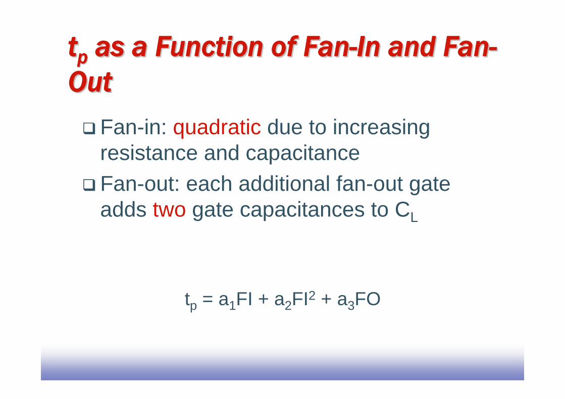
ttpp as a Function of Fanas a Function of Fan--In and FanIn and Fan--OutOut
Fan-in: quadratic due to increasing resistance and capacitanceFan-out: each additional fan-out gate adds two gate capacitances to CL
tp = a1FI + a2FI2 + a3FO

EE14122
Design Techniques for large fanDesign Techniques for large fan--ininTransistor sizing
as long as fan-out capacitance dominatesProgressive sizingInN CL
C3
C2
C1In1
In2
In3
M1
M2
M3
MNDistributed RC line
M1 > M2 > M3 > … > MN(the fet closest to theoutput is the smallest)
Can reduce delay by more than 20%; decreasing gains as technology shrinks

EE14123
Transistor ordering
C2
C1In1
In2
In3
M1
M2
M3 CL
C2
C1In3
In2
In1
M1
M2
M3 CL
critical path critical path
charged1
0→1charged
charged1
delay determined by time to discharge CL, C1 and C2
delay determined by time to discharge CL
1
1
0→1 charged
discharged
discharged

EE14124
Alternative logic structures
F = ABCDEFGH

EE14125
Isolating fan-in from fan-out using buffer insertion
CLCL

EE14126
Power consumption in CMOS logic gatesPower consumption in CMOS logic gates

EE14127
A
B
C
ZX
A
BZ
X
Example illustrating the effect of signal correlations

EE14128
Glitching in Static CMOS

EE14129
Example: Chain of NAND Gates

EE14130
How to Cope with Glitching?
A
B
CD
A
B
C
D
,
,
,
A
B
CD
A
B
C
D
,
,
,
A
B
CD
A
B
C
D
,
,
,

EE14131
Reordering of inputs affects the circuit activity
A
B
C
ZX
C
B
A
ZY
P(A=1) = 0.5
P(B=1) = 0.2
P(C=1) = 0.1
Input ordering

EE14132
Time multiplexing resources

EE14133
RatioedRatioed LogicLogic
VDD
VSS
PDNIn1In2In3
F
RLLoad
VDD
VSS
In1In2In3
F
VDD
VSS
PDNIn1In2In3
FVSS
PDN
Resistive DepletionLoad
PMOSLoad
(a) resistive load (b) depletion load NMOS (c) pseudo-NMOS
VT < 0
Goal: to reduce the number of devices over complementary CMOS

EE14134
VDD
VSS
PDNIn1In2In3
F
RLLoadResistive
N transistors + Load
• VOH = VDD
• VOL = RPN
RPN + RL
• Assymetrical response
• Static power consumption
•
• tpL= 0.69 RLCL
Resistive Resistive LoadLoad

EE14135
Active LoadsActive LoadsVDD
VSS
In1In2In3
F
VDD
VSS
PDNIn1In2In3
F
VSS
PDN
DepletionLoad
PMOSLoad
depletion load NMOS pseudo-NMOS
VT < 0

EE14136
PseudoPseudo--NMOS Inverter VTCNMOS Inverter VTC
0.0 0.5 1.0 1.5 2.0 2.50.0
0.5
1.0
1.5
2.0
2.5
3.0
Vin [V]
Vou
t[V
]
W/Lp = 4
W/Lp = 2
W/Lp = 1
W/Lp = 0.25
W/Lp = 0.5

EE14137

EE14138
FourFour--input pseudoinput pseudo--NMOS NORNMOS NOR

EE14139
Improved LoadsImproved Loads
A B C D
F
CL
M1M2 M1 >> M2Enable
VDD
Adaptive Load

EE14140
Improved Loads (2)Improved Loads (2)VDD
VSS
PDN1
Out
VDD
VSS
PDN2
Out
AABB
M1 M2
Differential Cascode Voltage Switch Logic (DCVSL)

EE14141
0 0.2 0.4 0.6 0.8 1.0-0.5
0.5
1.5
2.5
Time [ns]
Vol
tage
[V] A B
A B
A,BA, B
DCVSL AND/NAND Transient ResponseDCVSL AND/NAND Transient Response

EE14142
PassPass--Transistor LogicTransistor LogicIn
puts Switch
Network
OutOut
A
B
B
B
• N transistors• No static consumption

EE14143
Example: AND GateExample: AND Gate
B
B
A
F = AB
0

EE14144
NMOSNMOS--only Switchonly Switch
A = 2.5 V
X
C = 2.5 V
CL
A = 2.5 V
C = 2.5 V
XM2
M1
Mn
Threshold voltage loss causesstatic power consumption
VB does not pull up to 2.5V, but 2.5V -VTN
NMOS has higher threshold than PMOS (body effect)

EE14145
NMOSNMOS--Only LogicOnly Logic
VDD
In
Outx
0.5μm/0.25μm0.5μm/0.25μm
1.5μm/0.25μm
0 0.5 1 1.5 20.0
1.0
2.0
3.0
Time [ns]
Volta
ge[V
] xOut
In

EE14146
Pass-transistor output (drain-source) terminal should not drive other terminals to avoid multiple threshold drops

EE14147
PassPass--Transistor AND Gate VTCTransistor AND Gate VTC

EE14148
NMOS Only Logic: NMOS Only Logic: Level Restoring TransistorLevel Restoring Transistor
M2
M1
Mn
Mr
OutA
B
VDDVDDLevel Restorer
X
• Advantage: Full Swing• Restorer adds capacitance, takes away pull down current at X• Ratio problem

EE14149
Restorer SizingRestorer Sizing
0 100 200 300 400 5000.0
1.0
2.0
W / Lr
=1.0/0.25 W /L r =1.25/0.25
W /Lr
=1.50/0.25
W /L r =1.75/0.25
Vo l
tag e
[V]
Time [ps]
3.0
W/Ln= 0.5/0.25
Upper limit on restorer size
EE14150
Transmission GateTransmission Gate
A B
C
C
A B
C
C
BCL
C = 0 V
A = 2.5 V
C = 2.5 V

EE14151
Transmission Gate XORTransmission Gate XOR
A
B
F
B
A
B
BM1
M2
M3/M4

EE14152
Resistance of Transmission GateResistance of Transmission Gate
Vout
0 V
2.5 V
2.5 VRn
Rp
0.0 1.0 2.00
10
20
30
Vout, V
Res
ista
nce,
ohm
s
Rn
Rp
Rn || RpRes
ista
nce,
Koh
ms
Vou t
0 V
2.5 V
2.5 VRn
Rp
0.0 1.0 2.00
10
20
30
Vout, V
Res
ista
nce,
ohm
s
Rn
Rp
Rn || Rp
Vout
0 V
2.5 V
2.5 VRn
Rp
0.0 1.0 2.00
10
20
30
Vout, V
Res
ista
nce,
ohm
s
Rn
Rp
Rn || RpRes
ista
nce,
Koh
ms
(W/L)p = (W/L)n = 0.5/0.25

EE14153
Delay in Transmission Gate NetworksDelay in Transmission Gate NetworksV 1 V i-1
C
2.5 2.5
0 0
V i V i+1
CC
2.5
0
V n-1 V n
CC
2.5
0
In
V 1 V i V i+1
C
V n-1 V n
CC
In
R eqR eq R eq R eq
CC
(a)
(b)
C
R eq R eq
C C
R eq
C C
R eq R eq
C C
R eq
C
In
m
(c)

EE14154
Delay OptimizationDelay Optimization