Embed Size (px)
Citation preview
CMOS Image Sensors in Cell Phones, Cars and Beyond
Patrick Feng
General manager BYD Microelectronics
October 8, 2013
2
BYD Microelectronics (BME) is a subsidiary of BYD Company
Limited, Shenzhen, China. Formed in 2004, BME focuses on
CMOS image sensors, touch solutions, power management IC,
and power devices.
CMOS Image Sensor (CIS) Markets
CIS Applications and Requirements
CIS Technical Efforts
1
2
3
CONTENTS
3
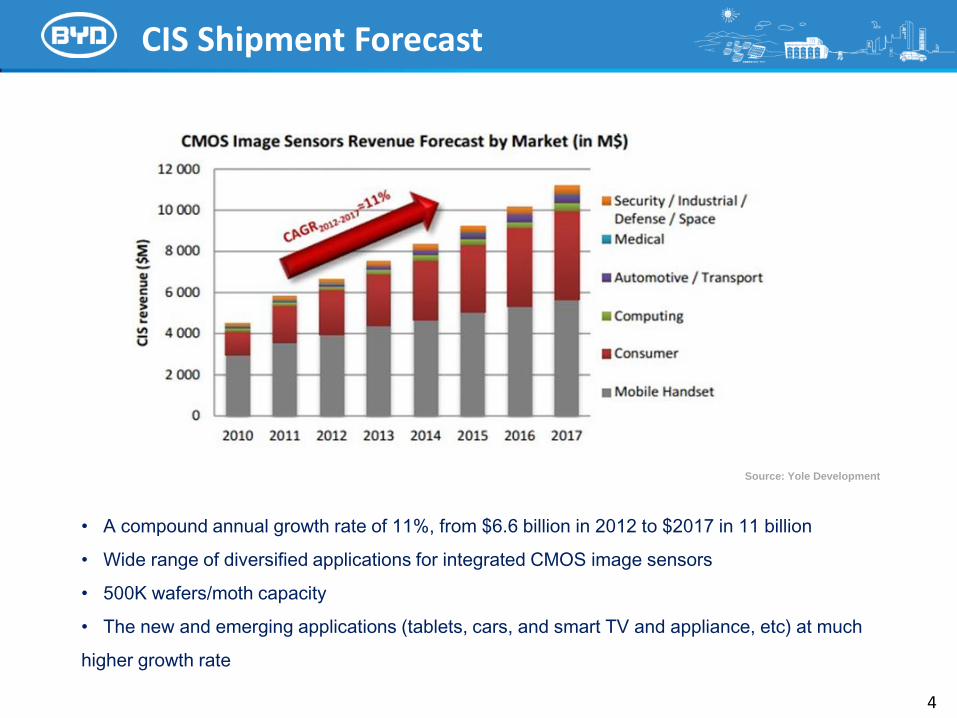
CIS Shipment Forecast
4
• A compound annual growth rate of 11%, from $6.6 billion in 2012 to $2017 in 11 billion
• Wide range of diversified applications for integrated CMOS image sensors
• 500K wafers/moth capacity
• The new and emerging applications (tablets, cars, and smart TV and appliance, etc) at much
higher growth rate
Source: Yole Development
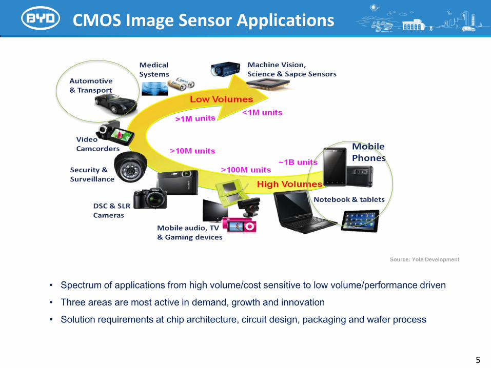
CMOS Image Sensor Applications
5
• Spectrum of applications from high volume/cost sensitive to low volume/performance driven
• Three areas are most active in demand, growth and innovation
• Solution requirements at chip architecture, circuit design, packaging and wafer process
Source: Yole Development
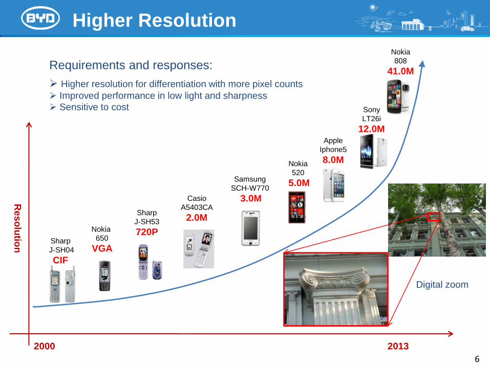
Higher Resolution
6
Sharp
J-SH04
CIF
Nokia
650
VGA
Sharp
J-SH53
720P
Nokia
808
41.0M
Sony
LT26i
12.0M Apple
Iphone5
8.0M
Casio
A5403CA
2.0M
Nokia
520
5.0M Samsung
SCH-W770
3.0M
Requirements and responses:
Higher resolution for differentiation with more pixel counts
Improved performance in low light and sharpness
Sensitive to cost
Digital zoom
Re
so
lutio
n
2000 2013
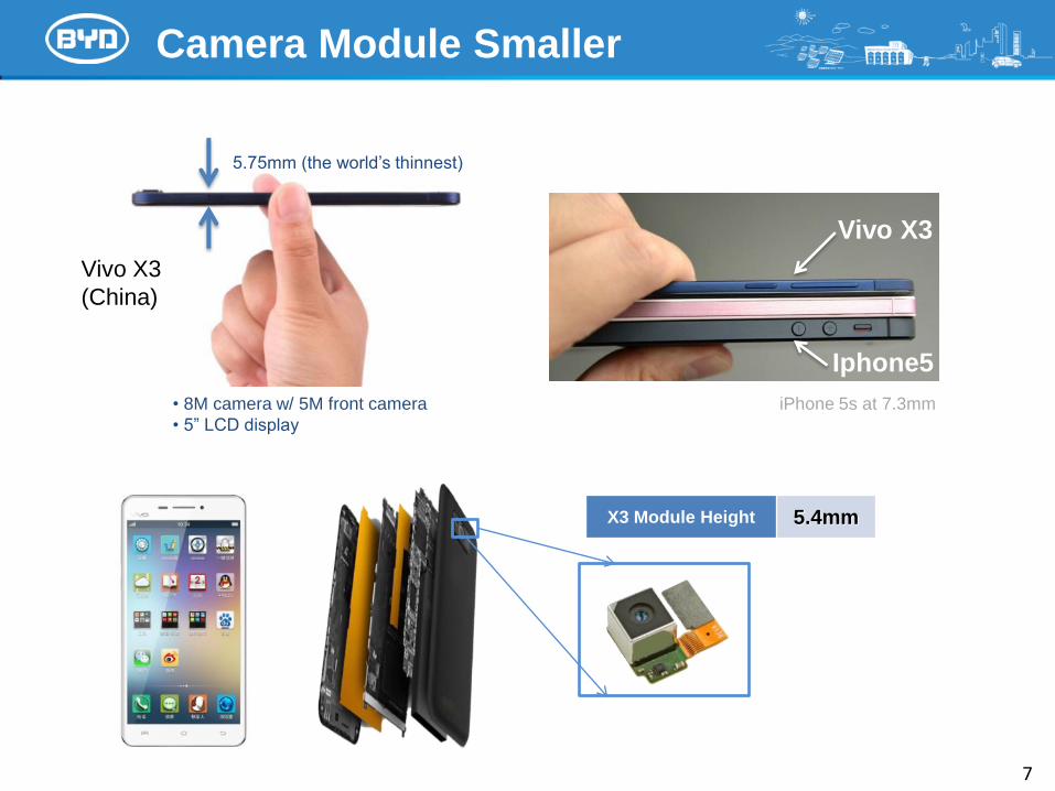
Camera Module Smaller
7
Vivo X3
Iphone5
Vivo X3
(China)
5.75mm (the world’s thinnest)
X3 Module Height 5.4mm
• 8M camera w/ 5M front camera
• 5” LCD display
iPhone 5s at 7.3mm
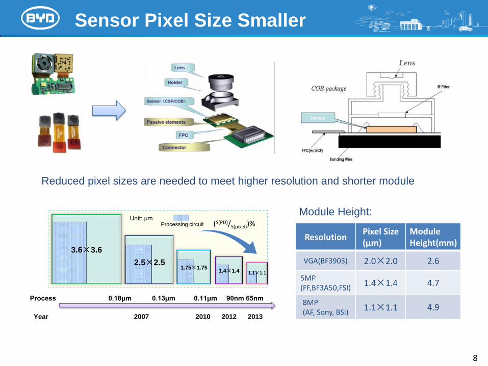
Sensor Pixel Size Smaller
8
Lens
Reduced pixel sizes are needed to meet higher resolution and shorter module
Processing circuit
(S(PD)/S(pixel))%
Process 0.18μm 0.13μm 0.11μm 90nm 65nm
Resolution Pixel Size (μm)
Module Height(mm)
VGA(BF3903) 2.0× 2.0 2.6
5MP (FF,BF3A50,FSI)
1.4× 1.4 4.7
8MP (AF, Sony, BSI)
1.1× 1.1 4.9
3.6× 3.6
Unit: μm
2.5× 2.5 1.75× 1.75
1.4× 1.4 1.1× 1.1
Year 2007 2010 2012 2013
Module Height:
Sensor Performance Challenge
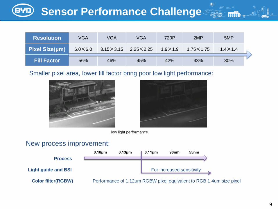
9
Resolution VGA VGA VGA 720P 2MP 5MP
Pixel Size(μm) 6.0× 6.0 3.15× 3.15 2.25× 2.25 1.9× 1.9 1.75× 1.75 1.4× 1.4
Fill Factor 56% 46% 45% 42% 43% 30%
Smaller pixel area, lower fill factor bring poor low light performance:
0.18μm 0.13μm 0.11μm 90nm 55nm
Process
Light guide and BSI For increased sensitivity
Color filter(RGBW) Performance of 1.12um RGBW pixel equivalent to RGB 1.4um size pixel
low light performance
New process improvement:
Sensor Cost Efforts
10
Resolution Process Pixel Size (μm)
Die numbers (pcs)
VGA(BF3403) 0.18μm 2.8× 2.8 2618
VGA(BF3703) 0.13μm 2.25× 2.25 4784
VGA(BF3903) 0.13μm 2.0× 2.0 5524
2MP(BF3920) 0.13μm 1.75× 1.75 1716
5MP(BF3A50) 0.11μm 1.4× 1.4 1134 8’’ Wafer
(CMOS Image Sensor)
Cost reduction through wafer process and design improvement
2618
4784
5524
$0.34
$0.13 $0.12
$0.00
$0.05
$0.10
$0.15
$0.20
$0.25
$0.30
$0.35
$0.40
0
1000
2000
3000
4000
5000
6000
2.8×2.8 0.18μm
2.25×2.25 0.13μm
2.0×2.0 0.13μm
Industry’s Effort and Results
Die numbers(pcs) Cost per Die
Cost per Die Die counts
11
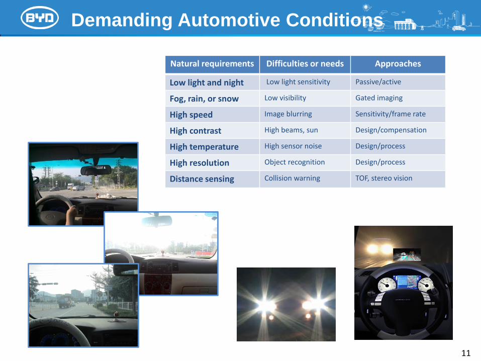
Demanding Automotive Conditions
Natural requirements Difficulties or needs Approaches
Low light and night Low light sensitivity Passive/active
Fog, rain, or snow Low visibility Gated imaging
High speed Image blurring Sensitivity/frame rate
High contrast High beams, sun Design/compensation
High temperature High sensor noise Design/process
High resolution Object recognition Design/process
Distance sensing Collision warning TOF, stereo vision
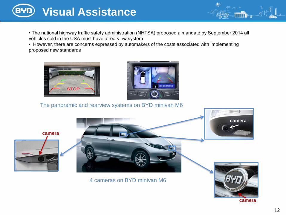
Visual Assistance
12 12
The panoramic and rearview systems on BYD minivan M6
• The national highway traffic safety administration (NHTSA) proposed a mandate by September 2014 all
vehicles sold in the USA must have a rearview system
• However, there are concerns expressed by automakers of the costs associated with implementing
proposed new standards
Camera
camera
camera
camera
4 cameras on BYD minivan M6
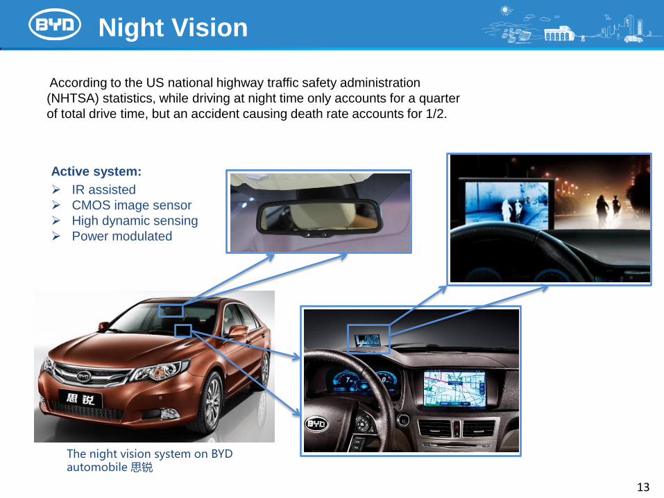
13
The night vision system on BYD automobile 思锐
According to the US national highway traffic safety administration
(NHTSA) statistics, while driving at night time only accounts for a quarter
of total drive time, but an accident causing death rate accounts for 1/2.
Night Vision
Active system:
IR assisted
CMOS image sensor
High dynamic sensing
Power modulated
14
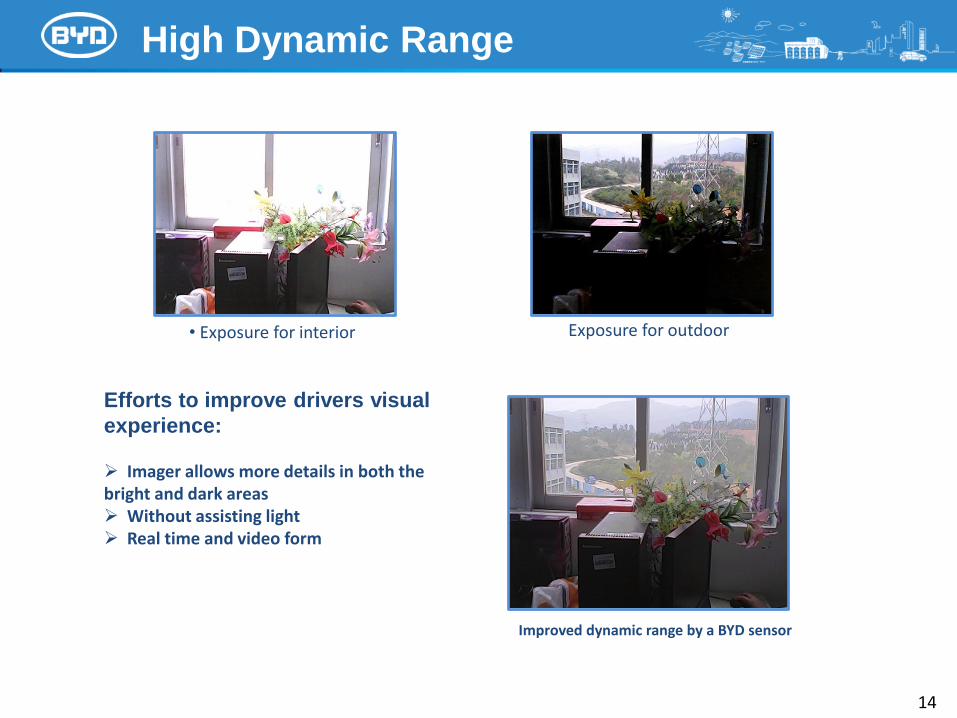
Exposure for outdoor
Improved dynamic range by a BYD sensor
• Exposure for interior
High Dynamic Range
Efforts to improve drivers visual
experience: Imager allows more details in both the bright and dark areas Without assisting light Real time and video form
15
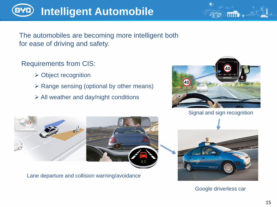
Lane departure and collision warning/avoidance
Object recognition
Range sensing (optional by other means)
All weather and day/night conditions
Google driverless car
Intelligent Automobile
The automobiles are becoming more intelligent both
for ease of driving and safety.
Signal and sign recognition
Requirements from CIS:
Papago
16
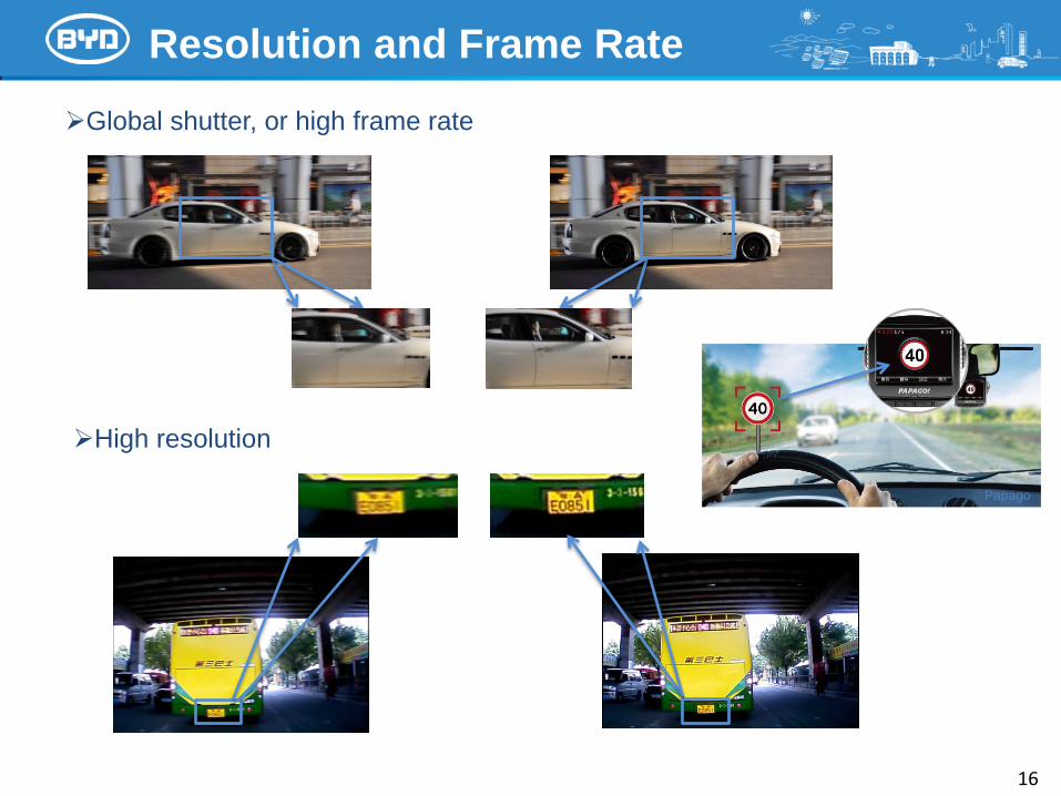
Resolution and Frame Rate
Global shutter, or high frame rate
High resolution
Papago
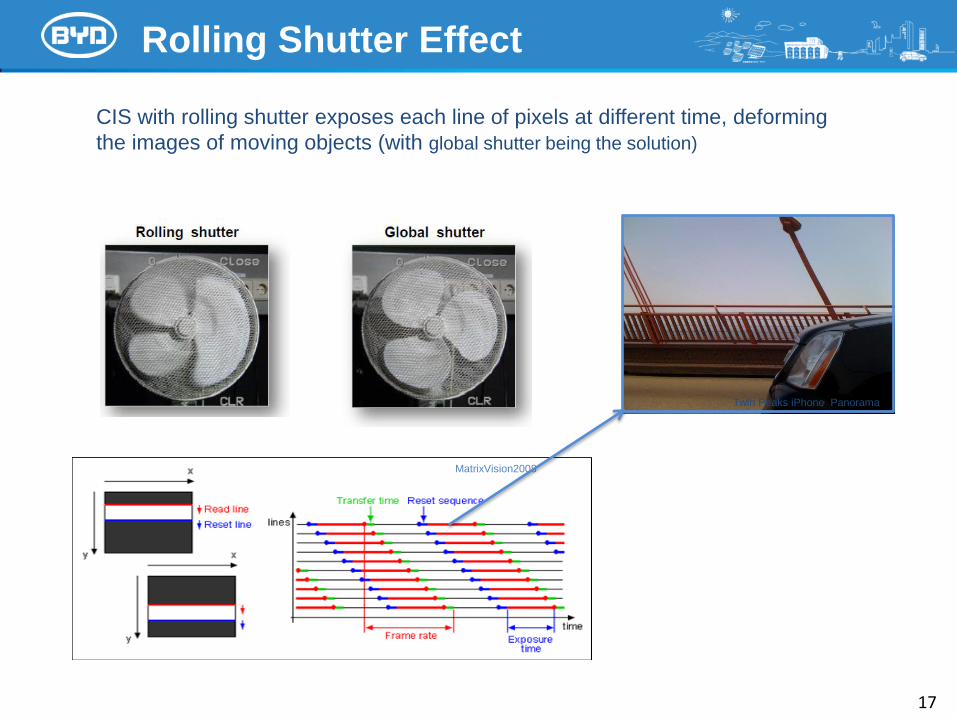
Rolling Shutter Effect
17
Twin Peaks iPhone Panorama
MatrixVision2008
CIS with rolling shutter exposes each line of pixels at different time, deforming
the images of moving objects (with global shutter being the solution)
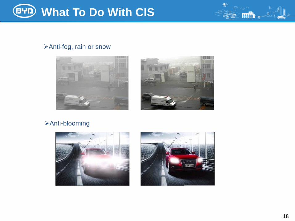
What To Do With CIS
18
Anti-fog, rain or snow
Anti-blooming
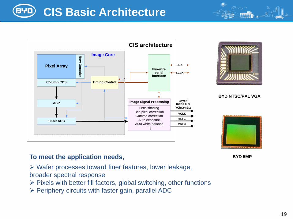
CIS Basic Architecture
19
Pixel Array
Column CDS
ASP
Ro
w D
ec
od
er
10-bit ADC
two-wire serial
Interface
Image Signal Processing Bayer/
RGB5:6:5/
YCbCr4:2:2
VCLK
HSYC
VSYC
SCLK
Lens shading
Bad pixel correction
Gamma correction
Auto exposure
Auto white balance
Timing Control
SDA
Image Core
……
CIS architecture
To meet the application needs,
Wafer processes toward finer features, lower leakage,
broader spectral response
Pixels with better fill factors, global switching, other functions
Periphery circuits with faster gain, parallel ADC
BYD NTSC/PAL VGA
BYD 5MP

FSI With Light Guide
20
Standard FSI FSI with
Light guide
480mV/Lux.s 600mV/Lux.s
• Light Guide Process Standard FSI
FSI with Light guide
Better sensitivity and uniformity
• Sensitivity improvement of 25-45%
• Uniformity improvement of 30%
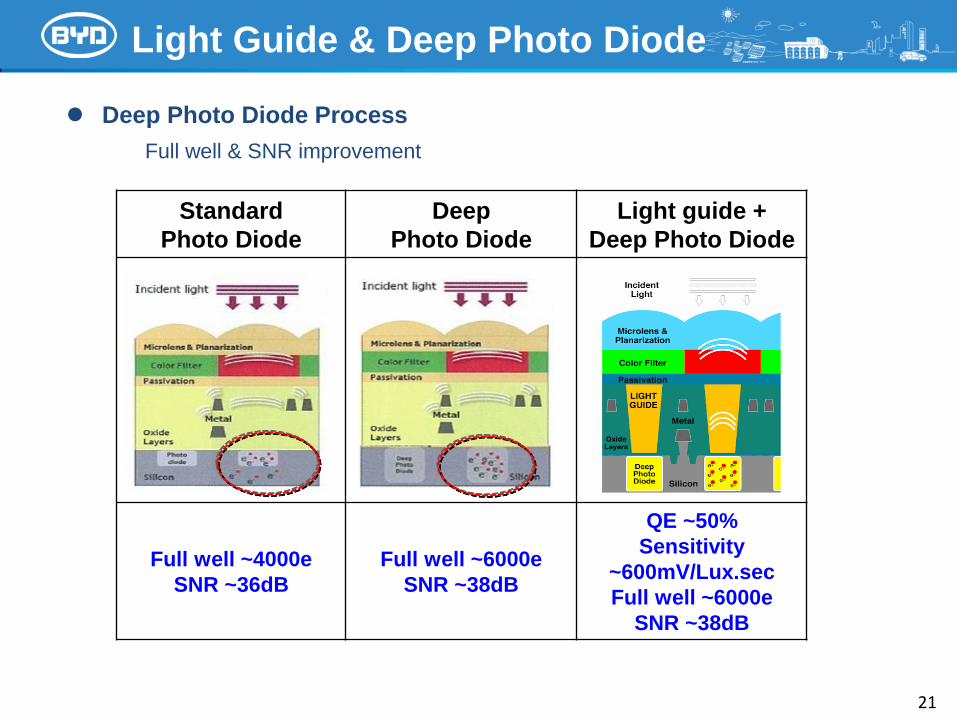
Light Guide & Deep Photo Diode
21
Standard
Photo Diode
Deep
Photo Diode
Light guide +
Deep Photo Diode
Full well ~4000e
SNR ~36dB
Full well ~6000e
SNR ~38dB
QE ~50%
Sensitivity
~600mV/Lux.sec
Full well ~6000e
SNR ~38dB
Deep Photo Diode Process
Full well & SNR improvement
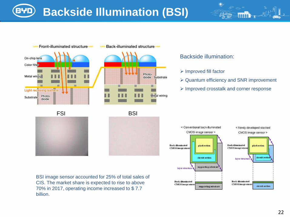
Backside Illumination (BSI)
22
Backside illumination:
Improved fill factor
Quantum efficiency and SNR improvement
Improved crosstalk and corner response
BSI image sensor accounted for 25% of total sales of
CIS. The market share is expected to rise to above
70% in 2017, operating income increased to $ 7.7
billion.
BSI FSI
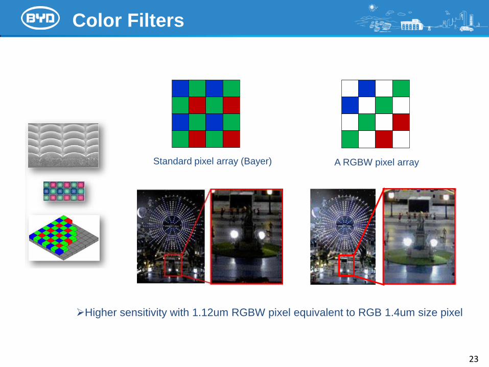
Color Filters
23
Standard pixel array (Bayer) A RGBW pixel array
Higher sensitivity with 1.12um RGBW pixel equivalent to RGB 1.4um size pixel
24
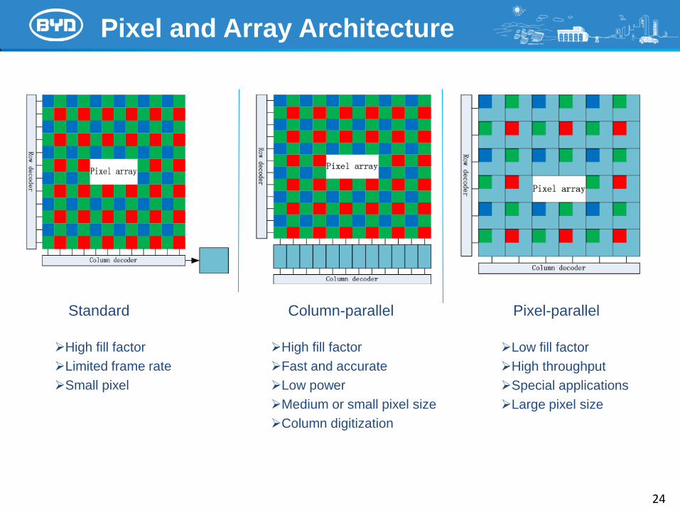
Pixel and Array Architecture
Standard Column-parallel Pixel-parallel
High fill factor
Fast and accurate
Low power
Medium or small pixel size
Column digitization
Low fill factor
High throughput
Special applications
Large pixel size
High fill factor
Limited frame rate
Small pixel
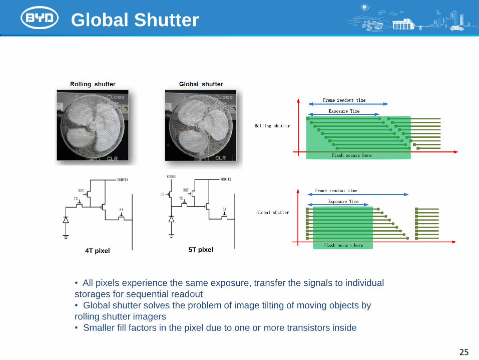
Global Shutter
25
• All pixels experience the same exposure, transfer the signals to individual
storages for sequential readout
• Global shutter solves the problem of image tilting of moving objects by
rolling shutter imagers
• Smaller fill factors in the pixel due to one or more transistors inside
4T pixel 5T pixel
26
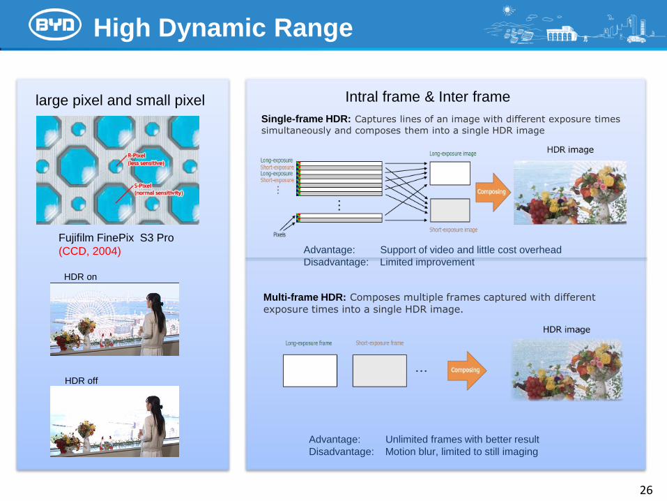
High Dynamic Range
Single-frame HDR: Captures lines of an image with different exposure times
simultaneously and composes them into a single HDR image
Multi-frame HDR: Composes multiple frames captured with different
exposure times into a single HDR image.
Intral frame & Inter frame
Fujifilm FinePix S3 Pro
(CCD, 2004)
large pixel and small pixel
Advantage: Support of video and little cost overhead
Disadvantage: Limited improvement
Advantage: Unlimited frames with better result
Disadvantage: Motion blur, limited to still imaging
HDR on
HDR off
Summary
27
CMOS image sensors for cellphones and automobiles/
surveillance present exciting but different types of
challenges
Collective efforts in wafer processing, imager design
and system applications are providing end users better
solutions
There are areas that need technical solutions,
especially for the automotive applications.

Questions?

Thanks


![[Tutorial] CMOS Image Sensors.pdf](https://img.pdfslide.us/doc/110x75/55cf9c66550346d033a9b510/tutorial-cmos-image-sensorspdf.jpg)