Embed Size (px)
Citation preview

CMOS FabricationCMOS FabricationCMOS FabricationCMOS Fabrication
EMT 251EMT 251
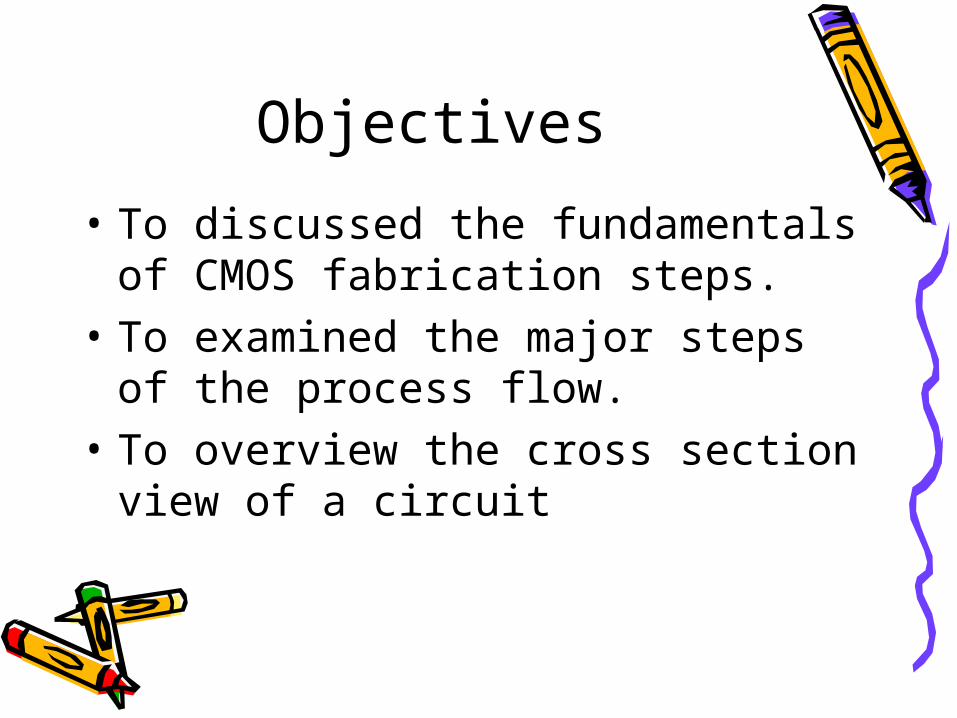
Objectives
• To discussed the fundamentals of CMOS fabrication steps.
• To examined the major steps of the process flow.
• To overview the cross section view of a circuit

• Photolithography (photo)– Process of transferring pattern on mask to photoresist
layer on wafer surface (pre-pattern the chip)• Etching
– Process of permanently removed the unwanted part of design on wafer surface to get the desired pattern
• Diffusion– Process of introducing dophant layer by movement of
dophant atoms from high concentration to low concentration area at high temperature
• Ion implantation– Process of introducing dophant layer by bombardment
of high energy dophant ion in high electric field chamber
• Oxidation– Process of growing thick or thin SiO2 layer depend on
oxide application• CMP
– Process to physically grind flat to have a planar surface for better exposure at photo process.

Chip making Process
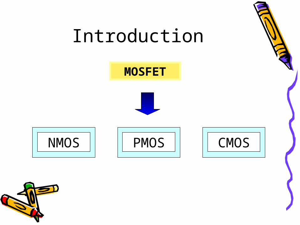
Introduction
MOSFET
CMOSPMOSNMOS

SourceDrain
Gate
Metal Oxide Semiconductor Field Effect Transistor
Source (Arsenic, Phosphorous, Boron)
Drain (Arsenic, Phosphorous, Boron)
Gate (Aluminum, Polysilicon)
MOSFET

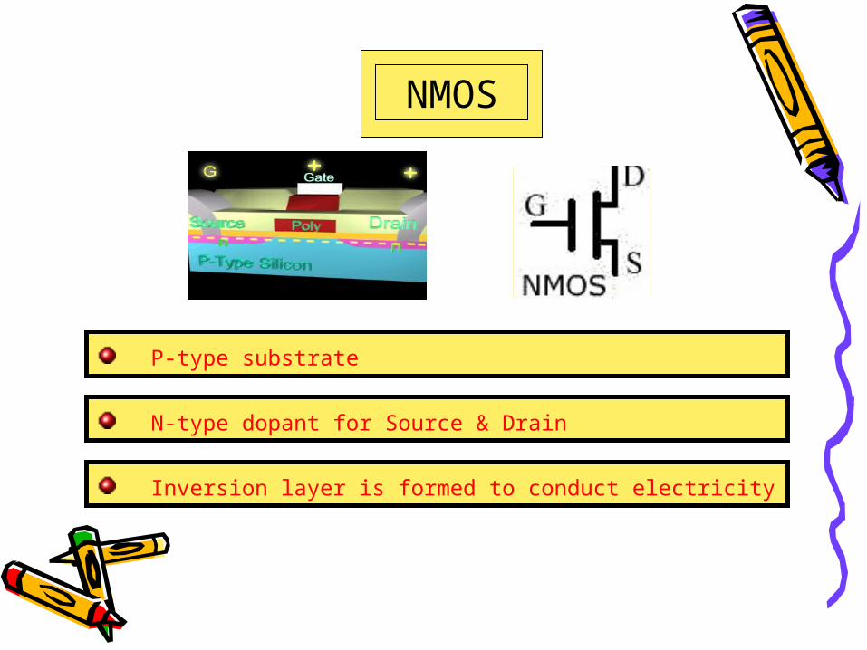
NMOS
P-type substrate
N-type dopant for Source & Drain
Inversion layer is formed to conduct electricity
NMOS
P-type substrate
N-type dopant for Source & Drain
Inversion layer is formed to conduct electricity

PMOS
N-type substrate
P-type dopant for Source & Drain
Inversion layer is formed to conduct electricity

PMOS
N-type substrate
P-type dopant for Source & Drain
Inversion layer is formed to conduct electricity

CMOS
A combination of both NMOS & PMOS technology
Most basic example: inverter

WELL FORMATIONWELL FORMATION
ISOLATION FORMATIONISOLATION FORMATION
TRANSISTOR MAKINGTRANSISTOR MAKING
INTERCONNECTIONINTERCONNECTION
PASSIVATIONPASSIVATION
PROCESS FLOW
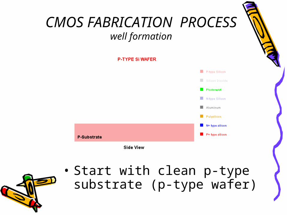
CMOS FABRICATION PROCESSwell formation
• Start with clean p-type substrate (p-type wafer)

CMOS FABRICATION PROCESSwell formation
• Grow epitaxy layer (made from SiO2) as mask layer for well formation

CMOS FABRICATION PROCESSwell formation
• By *photolithography and etching process, well opening are made
*photolithography and etch processes are shown in next slides
Well will be formed here
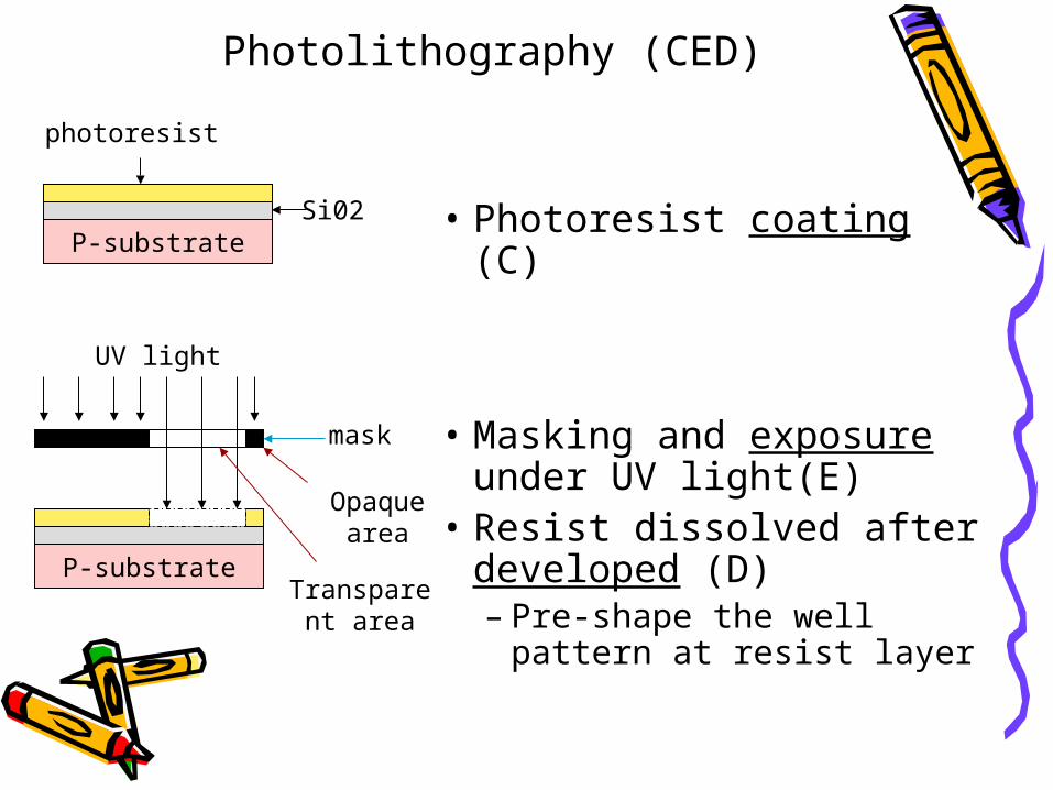
Photolithography (CED)
P-substrateSi02
photoresist
• Photoresist coating (C)
• Masking and exposure under UV light(E)
• Resist dissolved after developed (D)– Pre-shape the well
pattern at resist layer
P-substrate
mask
UV light
Opaque area
Transparent area

etching
• Removing the unwanted pattern by wet etching
• Resist clean• Desired pattern
formed
P-substrate
P-substrate

CMOS FABRICATION PROCESSwell formation
• Ion bombardment by ion implantation• SiO2 as mask, uncovered area will
exposed to dophant ion
Phosphorus ion

CMOS FABRICATION PROCESSisolation formation
• Increase SiO2 thickness by oxidation at high temperature
• Oxide will electrically isolates nmos and pmos devices
Thick oxide

CMOS FABRICATION PROCESStransistor making
• By photolithography and etching process, pmos and nmos areas are defined
pmos will be formed
here
nmos will be formed
here
LOCOS (isolation structure)

CMOS FABRICATION PROCESStransistor making
• Grow very thin gate oxide at elevated temperature in very short time
Gate oxide

• Deposit polisilicon layer
CMOS FABRICATION PROCESStransistor making
polisilicon

• Photolithography (photo) and etching to form gate pattern
CMOS FABRICATION PROCESStransistor making
gate

CMOS FABRICATION PROCESStransistor making
• Photo process to define the nmos’s active (source and drain) area and VDD contact
• Ion implantation with Arsenic ion for n+ dophant.
• Photoresist and polisilicon gate act as mask
photoresist
Arsenic ion

CMOS FABRICATION PROCESStransistor making
• Nmos’s Source and drain with VDD contact formation
• Resist removal
source drainVDD
contact

CMOS FABRICATION PROCESStransistor making
• Photo process to define the GND contact and pmos’s active area (source and drain)
• Ion implantation with boron ionto have p+ dophant
• Photoresist and gate act as mask
Boron ion
photoresist

CMOS FABRICATION PROCESStransistor making
• Pmos’s source and drain formation with GND contact
• Resist removal
GND contact Pmos’
source
Pmos’s drain

CMOS FABRICATION PROCESSinterconnection
• Deposit SiO2 layer through out wafer surface
SiO2

• Photo and etching process to make contact
CMOS FABRICATION PROCESSinterconnection
contact

• Metal 1 deposition throughout wafer surface
CMOS FABRICATION PROCESSinterconnection
Metal 1
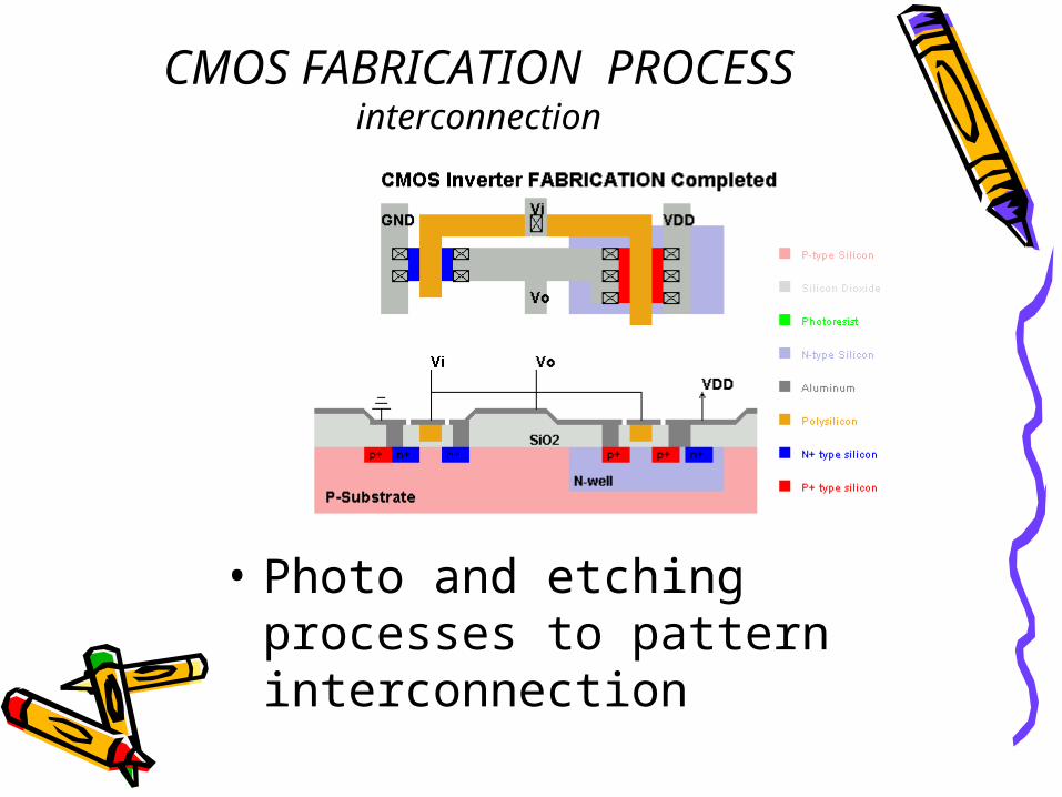
CMOS FABRICATION PROCESSinterconnection
• Photo and etching processes to pattern interconnection

Mask Layout

Mask Layout

Mask Layout

Mask Layout

AA’
oxide
p-substrate
n+ n+
N-well
p+p+
Metal 1
n+

ExerciseB
B’
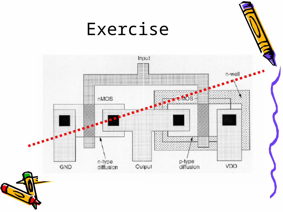
Exercise

GLOSSARY• Photolithography (photo)
– Process of transferring pattern on mask to photoresist layer on wafer surface (pre-pattern the chip)
• Etching– Process of permanently removed the unwanted part of design on
wafer surface to get the desired pattern• Diffusion
– Process of introducing dophant layer by movement of dophant atoms from high concentration to low concentration area at high temperature
• Ion implantation– Process of introducing dophant layer by bombardment of high
energy dophant ion in high electric field chamber• Oxidation
– Process of growing thick or thin SiO2 layer depend on oxide application
• CMP– Process to physically grind flat to have a planar surface for better
exposure at photo process.

THE END


![CMOS Fabrication [Compatibility Mode]](https://img.pdfslide.us/doc/110x75/577cdf861a28ab9e78b17027/cmos-fabrication-compatibility-mode.jpg)