Embed Size (px)
Citation preview

Rev. 1.1
CMOS 16-BIT SINGLE CHIP MICROCONTROLLER
S1C17W12/W13Technical Manual

© SEIKO EPSON CORPORATION 2017, All rights reserved.
NOTICENo part of this material may be reproduced or duplicated in any form or by any means without the written permission of Seiko Epson. Seiko Epson reserves the right to make changes to this material without notice. Seiko Epson does not assume any liability of any kind arising out of any inaccuracies contained in this material or due to its application or use in any product or circuit and, further, there is no representation that this material is applicable to products requiring high level reliability, such as, medical prod-ucts. Moreover, no license to any intellectual property rights is granted by implication or otherwise, and there is no representation or warranty that anything made in accordance with this material will be free from any patent or copyright infringement of a third party. When exporting the products or technology described in this material, you should comply with the applicable export control laws and regulations and follow the procedures required by such laws and regulations. You are requested not to use, to resell, to export and/or to otherwise dispose of the products (and any technical information furnished, if any) for the development and/or manufacture of weapon of mass destruction or for other military purposes.
All brands or product names mentioned herein are trademarks and/or registered trademarks of their respective companies.

DevicesS1 C 17xxx F 00E1
Packing specifications 00 : Besides tape & reel 0A : TCP BL 2 directions 0B : Tape & reel BACK 0C : TCP BR 2 directions 0D : TCP BT 2 directions 0E : TCP BD 2 directions 0F : Tape & reel FRONT 0G : TCP BT 4 directions 0H : TCP BD 4 directions 0J : TCP SL 2 directions 0K : TCP SR 2 directions 0L : Tape & reel LEFT 0M : TCP ST 2 directions 0N : TCP SD 2 directions 0P : TCP ST 4 directions 0Q : TCP SD 4 directions 0R : Tape & reel RIGHT 99 : Specs not fixed
Specification
Package D: die form; F: QFP, B: BGA, WCSP
Model number
Model name C: microcomputer, digital products
Product classification S1: semiconductor
Development toolsS5U1 C 17000 H2 1
Packing specifications 00: standard packing
Version 1: Version 1
Tool type Hx : ICE Dx : Evaluation board Ex : ROM emulation board Mx : Emulation memory for external ROM Tx : A socket for mounting
Cx : Compiler package Sx : Middleware package Yx : Writer software
Corresponding model number 17xxx: for S1C17xxx
Tool classification C: microcomputer use
Product classification S5U1: development tool for semiconductor products
00
00
Configuration of product number
CONFIGURATION OF PRODUCT NUMBER
S1C17W12/W13 TECHNICAL MANUAL Seiko Epson Corporation i(Rev. 1.1)
Configuration of product number

PREFACE
ii Seiko Epson Corporation S1C17W12/W13 TECHNICAL MANUAL (Rev. 1.1)
Preface This is a technical manual for designers and programmers who develop a product using the S1C17W12/W13.
This document describes the functions of the IC, embedded peripheral circuit operations, and their control methods.
For the CPU functions and instructions, refer to the “S1C17 Family S1C17 Core Manual.” For the functions and operations of the debugging tools, refer to the respective tool manuals. (Our “Products: Document Down-loads” website provides the downloadable manuals.)
Notational conventions and symbols in this manual Register address
Peripheral circuit chapters do not provide control register addresses. Refer to “Peripheral Circuit Area” in the “Memory and Bus” chapter or “List of Peripheral Circuit Control Registers” in the Appendix.
Register and control bit names In this manual, the register and control bit names are described as shown below to distinguish from signal
and pin names.XXX register: Represents a register including its all bits.XXX.YYY bit: Represents the one control bit YYY in the XXX register.XXX.ZZZ[1:0] bits: Represents the two control bits ZZZ1 and ZZZ0 in the XXX register.
Register table contents and symbolsInitial: Value set at initialization
Reset: Initialization condition. The initialization condition depends on the reset group (H0, H1, or S0). For more information on the reset groups, refer to “Initialization Conditions (Reset Groups)” in the “Power Supply, Reset, and Clocks” chapter.
R/W: R = Read only bit W = Write only bit WP = Write only bit with a write protection using the MSCPROT.PROT[15:0] bits R/W = Read/write bit R/WP = Read/write bit with a write protection using the MSCPROT.PROT[15:0] bits
Control bit read/write values This manual describes control bit values in a hexadecimal notation except for one-bit values (and except
when decimal or binary notation is required in terms of explanation). The values are described as shown below according to the control bit width.
1 bit: 0 or 1 2 to 4 bits: 0x0 to 0xf 5 to 8 bits: 0x00 to 0xff 9 to 12 bits: 0x000 to 0xfff 13 to 16 bits: 0x0000 to 0xffff
Decimal: 0 to 9999... Binary: 0b0000... to 0b1111...
Channel number Multiple channels may be implemented in some peripheral circuits (e.g., 16-bit timer, etc.). The peripheral
circuit chapters use ‘n’ as the value that represents the channel number in the register and pin names regard-less of the number of channel actually implemented. Normally, the descriptions are applied to all channels. If there is a channel that has different functions from others, the channel number is specified clearly.Example) T16_nCTL register of the 16-bit timer If one channel is implemented (Ch.0 only): T16_nCTL = T16_0CTL only If two channels are implemented (Ch.0 and Ch.1): T16_nCTL = T16_0CTL and T16_1CTL
For the number of channels implemented in the peripheral circuits of this IC, refer to “Features” in the “Overview” chapter.

CONTENTS
S1C17W12/W13 TECHNICAL MANUAL Seiko Epson Corporation iii(Rev. 1.1)
– Contents –
Configuration of product number..............................................................................................iPreface ..................................................................................................................................... iiNotational conventions and symbols in this manual ............................................................... ii
1 Overview ........................................................................................................................1-11.1 Features .......................................................................................................................... 1-11.2 Block Diagram ................................................................................................................. 1-41.3 Pins ................................................................................................................................. 1-6
1.3.1 Pin Configuration Diagram (Package) ............................................................... 1-61.3.2 Pad Configuration Diagram (Chip) ................................................................... 1-101.3.3 Pin Descriptions ............................................................................................... 1-11
2 Power Supply, Reset, and Clocks ...............................................................................2-12.1 Power Generator (PWG2) ................................................................................................ 2-1
2.1.1 Overview ........................................................................................................... 2-12.1.2 Pins ................................................................................................................... 2-12.1.3 Operations ........................................................................................................ 2-2
2.2 System Reset Controller (SRC) ....................................................................................... 2-42.2.1 Overview ........................................................................................................... 2-42.2.2 Input Pin ............................................................................................................ 2-42.2.3 Reset Sources .................................................................................................. 2-42.2.4 Initialization Conditions (Reset Groups) ............................................................ 2-5
2.3 Clock Generator (CLG) .................................................................................................... 2-62.3.1 Overview ........................................................................................................... 2-62.3.2 Input/Output Pins ............................................................................................. 2-72.3.3 Clock Sources .................................................................................................. 2-72.3.4 Operations ....................................................................................................... 2-10
2.4 Operating Mode ............................................................................................................. 2-152.4.1 Initial Boot Sequence ....................................................................................... 2-152.4.2 Transition between Operating Modes .............................................................. 2-15
2.5 Interrupts ........................................................................................................................ 2-172.6 Control Registers ........................................................................................................... 2-17
PWG2 Control Register ............................................................................................................ 2-17PWG2 Timing Control Register ................................................................................................ 2-18PWG2 Interrupt Flag Register .................................................................................................. 2-18PWG2 Interrupt Enable Register .............................................................................................. 2-18CLG System Clock Control Register ........................................................................................ 2-18CLG Oscillation Control Register ............................................................................................. 2-20CLG IOSC Control Register ..................................................................................................... 2-20CLG OSC1 Control Register .................................................................................................... 2-21CLG OSC3 Control Register .................................................................................................... 2-22CLG Interrupt Flag Register ..................................................................................................... 2-24CLG Interrupt Enable Register ................................................................................................. 2-24CLG FOUT Control Register ..................................................................................................... 2-25CLG Oscillation Frequency Trimming Register ........................................................................ 2-26
3 CPU and Debugger ......................................................................................................3-13.1 Overview ......................................................................................................................... 3-13.2 CPU Core ........................................................................................................................ 3-2
3.2.1 CPU Registers .................................................................................................. 3-23.2.2 Instruction Set .................................................................................................. 3-23.2.3 Reading PSR .................................................................................................... 3-23.2.4 I/O Area Reserved for the S1C17 Core ............................................................ 3-2

CONTENTS
iv Seiko Epson Corporation S1C17W12/W13 TECHNICAL MANUAL (Rev. 1.1)
3.3 Debugger ........................................................................................................................ 3-23.3.1 Debugging Functions........................................................................................ 3-23.3.2 Resource Requirements and Debugging Tools ................................................ 3-23.3.3 List of debugger input/output pins ................................................................... 3-33.3.4 External Connection ......................................................................................... 3-33.3.5 Flash Security Function .................................................................................... 3-3
3.4 Control Register .............................................................................................................. 3-4MISC PSR Register ................................................................................................................... 3-4Debug RAM Base Register ....................................................................................................... 3-4
4 Memory and Bus ..........................................................................................................4-14.1 Overview ......................................................................................................................... 4-14.2 Bus Access Cycle ........................................................................................................... 4-14.3 Flash Memory ................................................................................................................. 4-2
4.3.1 Flash Memory Pin ............................................................................................. 4-24.3.2 Flash Bus Access Cycle Setting ....................................................................... 4-24.3.3 Flash Programming ........................................................................................... 4-3
4.4 RAM ................................................................................................................................ 4-34.5 Display Data RAM ........................................................................................................... 4-34.6 Peripheral Circuit Control Registers ................................................................................ 4-4
4.6.1 System-Protect Function .................................................................................. 4-74.7 Control Registers ............................................................................................................ 4-7
MISC System Protect Register ................................................................................................. 4-7MISC IRAM Size Register.......................................................................................................... 4-8FLASHC Flash Read Cycle Register ......................................................................................... 4-8
5 Interrupt Controller (ITC) .............................................................................................5-15.1 Overview ......................................................................................................................... 5-15.2 Vector Table .................................................................................................................... 5-1
5.2.1 Vector Table Base Address (TTBR) ................................................................... 5-35.3 Initialization ..................................................................................................................... 5-35.4 Maskable Interrupt Control and Operations ................................................................... 5-3
5.4.1 Peripheral Circuit Interrupt Control ................................................................... 5-35.4.2 ITC Interrupt Request Processing .................................................................... 5-35.4.3 Conditions to Accept Interrupt Requests by the CPU...................................... 5-4
5.5 NMI .................................................................................................................................. 5-45.6 Software Interrupts ......................................................................................................... 5-45.7 Interrupt Processing by the CPU .................................................................................... 5-45.8 Control Registers ............................................................................................................ 5-5
MISC Vector Table Address Low Register ................................................................................ 5-5MISC Vector Table Address High Register ................................................................................ 5-5ITC Interrupt Level Setup Register x ......................................................................................... 5-5
6 I/O Ports (PPORT) .........................................................................................................6-16.1 Overview ......................................................................................................................... 6-16.2 I/O Cell Structure and Functions ..................................................................................... 6-2
6.2.1 Schmitt Input .................................................................................................... 6-36.2.2 Over Voltage Tolerant Fail-Safe Type I/O Cell ................................................... 6-36.2.3 Pull-Up/Pull-Down ............................................................................................ 6-36.2.4 CMOS Output and High Impedance State ....................................................... 6-36.2.5 LED Drive Pin .................................................................................................... 6-3
6.3 Clock Settings ................................................................................................................. 6-46.3.1 PPORT Operating Clock ................................................................................... 6-46.3.2 Clock Supply in SLEEP Mode .......................................................................... 6-4

CONTENTS
S1C17W12/W13 TECHNICAL MANUAL Seiko Epson Corporation v(Rev. 1.1)
6.3.3 Clock Supply in DEBUG Mode ......................................................................... 6-46.4 Operations ...................................................................................................................... 6-4
6.4.1 Initialization ....................................................................................................... 6-46.4.2 Port Input/Output Control ................................................................................. 6-6
6.5 Interrupts ......................................................................................................................... 6-76.6 Control Registers ............................................................................................................ 6-7
Px Port Data Register ................................................................................................................ 6-7Px Port Enable Register ............................................................................................................ 6-8Px Port Pull-up/down Control Register ..................................................................................... 6-8Px Port Interrupt Flag Register .................................................................................................. 6-9Px Port Interrupt Control Register ............................................................................................. 6-9Px Port Chattering Filter Enable Register .................................................................................. 6-9Px Port Mode Select Register ................................................................................................... 6-9Px Port Function Select Register ............................................................................................. 6-10P Port Clock Control Register .................................................................................................. 6-10P Port Interrupt Flag Group Register ........................................................................................ 6-11
6.7 Control Register and Port Function Configuration of this IC ......................................... 6-126.7.1 P0 Port Group .................................................................................................. 6-126.7.2 P1 Port Group .................................................................................................. 6-136.7.3 P2 Port Group .................................................................................................. 6-146.7.4 P3 Port Group .................................................................................................. 6-156.7.5 P4 Port Group .................................................................................................. 6-166.7.6 Pd Port Group .................................................................................................. 6-176.7.7 Common Registers between Port Groups....................................................... 6-18
7 Universal Port Multiplexer (UPMUX) ...........................................................................7-17.1 Overview ......................................................................................................................... 7-17.2 Peripheral Circuit I/O Function Assignment .................................................................... 7-17.3 Control Registers ............................................................................................................ 7-2
Pxy–xz Universal Port Multiplexer Setting Register ................................................................... 7-2
8 Watchdog Timer (WDT2) ..............................................................................................8-18.1 Overview ......................................................................................................................... 8-18.2 Clock Settings ................................................................................................................. 8-1
8.2.1 WDT2 Operating Clock ..................................................................................... 8-18.2.2 Clock Supply in DEBUG Mode ......................................................................... 8-1
8.3 Operations ...................................................................................................................... 8-28.3.1 WDT2 Control ................................................................................................... 8-28.3.2 Operations in HALT and SLEEP Modes............................................................ 8-3
8.4 Control Registers ............................................................................................................ 8-3WDT2 Clock Control Register ................................................................................................... 8-3WDT2 Control Register ............................................................................................................. 8-4WDT2 Counter Compare Match Register ................................................................................. 8-5
9 Real-Time Clock (RTCA) ..............................................................................................9-19.1 Overview ......................................................................................................................... 9-19.2 Output Pin and External Connection .............................................................................. 9-1
9.2.1 Output Pin ......................................................................................................... 9-19.3 Clock Settings ................................................................................................................. 9-2
9.3.1 RTCA Operating Clock ..................................................................................... 9-29.3.2 Theoretical Regulation Function ....................................................................... 9-2
9.4 Operations ...................................................................................................................... 9-39.4.1 RTCA Control ................................................................................................... 9-39.4.2 Real-Time Clock Counter Operations ............................................................... 9-49.4.3 Stopwatch Control ............................................................................................ 9-4
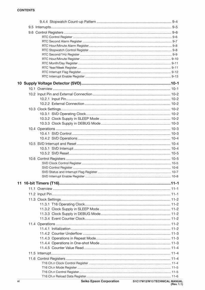
CONTENTS
vi Seiko Epson Corporation S1C17W12/W13 TECHNICAL MANUAL (Rev. 1.1)
9.4.4 Stopwatch Count-up Pattern ........................................................................... 9-49.5 Interrupts ......................................................................................................................... 9-59.6 Control Registers ............................................................................................................ 9-6
RTC Control Register ................................................................................................................ 9-6RTC Second Alarm Register ..................................................................................................... 9-7RTC Hour/Minute Alarm Register .............................................................................................. 9-8RTC Stopwatch Control Register .............................................................................................. 9-8RTC Second/1Hz Register ........................................................................................................ 9-9RTC Hour/Minute Register ....................................................................................................... 9-10RTC Month/Day Register ......................................................................................................... 9-11RTC Year/Week Register .......................................................................................................... 9-11RTC Interrupt Flag Register ...................................................................................................... 9-12RTC Interrupt Enable Register ................................................................................................. 9-13
10 Supply Voltage Detector (SVD) .................................................................................10-110.1 Overview ...................................................................................................................... 10-110.2 Input Pin and External Connection .............................................................................. 10-2
10.2.1 Input Pin ......................................................................................................... 10-210.2.2 External Connection ...................................................................................... 10-2
10.3 Clock Settings .............................................................................................................. 10-210.3.1 SVD Operating Clock ..................................................................................... 10-210.3.2 Clock Supply in SLEEP Mode ....................................................................... 10-210.3.3 Clock Supply in DEBUG Mode ...................................................................... 10-3
10.4 Operations ................................................................................................................... 10-310.4.1 SVD Control ................................................................................................... 10-310.4.2 SVD Operations ............................................................................................. 10-4
10.5 SVD Interrupt and Reset .............................................................................................. 10-410.5.1 SVD Interrupt ................................................................................................. 10-410.5.2 SVD Reset ...................................................................................................... 10-5
10.6 Control Registers ......................................................................................................... 10-5SVD Clock Control Register ..................................................................................................... 10-5SVD Control Register ............................................................................................................... 10-6SVD Status and Interrupt Flag Register ................................................................................... 10-7SVD Interrupt Enable Register ................................................................................................. 10-8
11 16-bit Timers (T16) .....................................................................................................11-111.1 Overview ...................................................................................................................... 11-111.2 Input Pin ....................................................................................................................... 11-111.3 Clock Settings .............................................................................................................. 11-2
11.3.1 T16 Operating Clock ...................................................................................... 11-211.3.2 Clock Supply in SLEEP Mode ....................................................................... 11-211.3.3 Clock Supply in DEBUG Mode ...................................................................... 11-211.3.4 Event Counter Clock ...................................................................................... 11-2
11.4 Operations ................................................................................................................... 11-211.4.1 Initialization .................................................................................................... 11-211.4.2 Counter Underflow ........................................................................................ 11-311.4.3 Operations in Repeat Mode ........................................................................... 11-311.4.4 Operations in One-shot Mode ....................................................................... 11-311.4.5 Counter Value Read ....................................................................................... 11-4
11.5 Interrupt ........................................................................................................................ 11-411.6 Control Registers ......................................................................................................... 11-4
T16 Ch.n Clock Control Register ............................................................................................. 11-4T16 Ch.n Mode Register .......................................................................................................... 11-5T16 Ch.n Control Register ........................................................................................................ 11-5T16 Ch.n Reload Data Register ................................................................................................ 11-6

CONTENTS
S1C17W12/W13 TECHNICAL MANUAL Seiko Epson Corporation vii(Rev. 1.1)
T16 Ch.n Counter Data Register .............................................................................................. 11-6T16 Ch.n Interrupt Flag Register .............................................................................................. 11-6T16 Ch.n Interrupt Enable Register .......................................................................................... 11-7
12 UART (UART2) ............................................................................................................12-112.1 Overview ...................................................................................................................... 12-112.2 Input/Output Pins and External Connections .............................................................. 12-2
12.2.1 List of Input/Output Pins ................................................................................ 12-212.2.2 External Connections .................................................................................... 12-212.2.3 Input Pin Pull-Up Function............................................................................. 12-212.2.4 Output Pin Open-Drain Output Function ...................................................... 12-212.2.5 Input/Output Signal Inverting Function .......................................................... 12-2
12.3 Clock Settings .............................................................................................................. 12-212.3.1 UART2 Operating Clock ................................................................................ 12-212.3.2 Clock Supply in SLEEP Mode ....................................................................... 12-312.3.3 Clock Supply in DEBUG Mode ...................................................................... 12-312.3.4 Baud Rate Generator ..................................................................................... 12-3
12.4 Data Format ................................................................................................................. 12-312.5 Operations ................................................................................................................... 12-4
12.5.1 Initialization .................................................................................................... 12-412.5.2 Data Transmission ......................................................................................... 12-512.5.3 Data Reception .............................................................................................. 12-612.5.4 IrDA Interface ................................................................................................. 12-7
12.6 Receive Errors .............................................................................................................. 12-712.6.1 Framing Error ................................................................................................. 12-712.6.2 Parity Error ..................................................................................................... 12-812.6.3 Overrun Error ................................................................................................. 12-8
12.7 Interrupts ...................................................................................................................... 12-812.8 Control Registers ......................................................................................................... 12-9
UART2 Ch.n Clock Control Register ........................................................................................ 12-9UART2 Ch.n Mode Register ..................................................................................................... 12-9UART2 Ch.n Baud–Rate Register ........................................................................................... 12-10UART2 Ch.n Control Register ................................................................................................. 12-11UART2 Ch.n Transmit Data Register ....................................................................................... 12-11UART2 Ch.n Receive Data Register ........................................................................................ 12-11UART2 Ch.n Status and Interrupt Flag Register ..................................................................... 12-12UART2 Ch.n Interrupt Enable Register.................................................................................... 12-13
13 Synchronous Serial Interface (SPIA) ........................................................................13-113.1 Overview ...................................................................................................................... 13-113.2 Input/Output Pins and External Connections .............................................................. 13-2
13.2.1 List of Input/Output Pins ................................................................................ 13-213.2.2 External Connections .................................................................................... 13-213.2.3 Pin Functions in Master Mode and Slave Mode ............................................ 13-313.2.4 Input Pin Pull-Up/Pull-Down Function .......................................................... 13-3
13.3 Clock Settings .............................................................................................................. 13-313.3.1 SPIA Operating Clock .................................................................................... 13-313.3.2 Clock Supply in DEBUG Mode ...................................................................... 13-413.3.3 SPI Clock (SPICLKn) Phase and Polarity ...................................................... 13-4
13.4 Data Format ................................................................................................................. 13-513.5 Operations ................................................................................................................... 13-5
13.5.1 Initialization .................................................................................................... 13-513.5.2 Data Transmission in Master Mode ............................................................... 13-513.5.3 Data Reception in Master Mode .................................................................... 13-7

CONTENTS
viii Seiko Epson Corporation S1C17W12/W13 TECHNICAL MANUAL (Rev. 1.1)
13.5.4 Terminating Data Transfer in Master Mode .................................................... 13-813.5.5 Data Transfer in Slave Mode .......................................................................... 13-813.5.6 Terminating Data Transfer in Slave Mode ..................................................... 13-10
13.6 Interrupts ..................................................................................................................... 13-1013.7 Control Registers ........................................................................................................ 13-11
SPIA Ch.n Mode Register ....................................................................................................... 13-11SPIA Ch.n Control Register ..................................................................................................... 13-12SPIA Ch.n Transmit Data Register .......................................................................................... 13-13SPIA Ch.n Receive Data Register ........................................................................................... 13-13SPIA Ch.n Interrupt Flag Register ........................................................................................... 13-13SPIA Ch.n Interrupt Enable Register ....................................................................................... 13-14
14 I2C (I2C) .......................................................................................................................14-114.1 Overview ...................................................................................................................... 14-114.2 Input/Output Pins and External Connections .............................................................. 14-2
14.2.1 List of Input/Output Pins ................................................................................ 14-214.2.2 External Connections .................................................................................... 14-2
14.3 Clock Settings .............................................................................................................. 14-314.3.1 I2C Operating Clock ...................................................................................... 14-314.3.2 Clock Supply in DEBUG Mode ...................................................................... 14-314.3.3 Baud Rate Generator ..................................................................................... 14-3
14.4 Operations ................................................................................................................... 14-414.4.1 Initialization .................................................................................................... 14-414.4.2 Data Transmission in Master Mode ............................................................... 14-514.4.3 Data Reception in Master Mode .................................................................... 14-714.4.4 10-bit Addressing in Master Mode ................................................................ 14-914.4.5 Data Transmission in Slave Mode................................................................. 14-1014.4.6 Data Reception in Slave Mode ..................................................................... 14-1214.4.7 Slave Operations in 10-bit Address Mode .................................................... 14-1414.4.8 Automatic Bus Clearing Operation ............................................................... 14-1414.4.9 Error Detection .............................................................................................. 14-15
14.5 Interrupts ..................................................................................................................... 14-1614.6 Control Registers ........................................................................................................ 14-17
I2C Ch.n Clock Control Register ............................................................................................. 14-17I2C Ch.n Mode Register .......................................................................................................... 14-18I2C Ch.n Baud-Rate Register .................................................................................................. 14-18I2C Ch.n Own Address Register ............................................................................................. 14-18I2C Ch.n Control Register ....................................................................................................... 14-19I2C Ch.n Transmit Data Register ............................................................................................. 14-20I2C Ch.n Receive Data Register .............................................................................................. 14-20I2C Ch.n Status and Interrupt Flag Register ........................................................................... 14-20I2C Ch.n Interrupt Enable Register ......................................................................................... 14-21
15 16-bit PWM Timers (T16B) ........................................................................................15-115.1 Overview ...................................................................................................................... 15-115.2 Input/Output Pins ......................................................................................................... 15-215.3 Clock Settings .............................................................................................................. 15-3
15.3.1 T16B Operating Clock ................................................................................... 15-315.3.2 Clock Supply in SLEEP Mode ....................................................................... 15-315.3.3 Clock Supply in DEBUG Mode ...................................................................... 15-315.3.4 Event Counter Clock ...................................................................................... 15-3
15.4 Operations ................................................................................................................... 15-415.4.1 Initialization .................................................................................................... 15-415.4.2 Counter Block Operations ............................................................................. 15-515.4.3 Comparator/Capture Block Operations ......................................................... 15-8

CONTENTS
S1C17W12/W13 TECHNICAL MANUAL Seiko Epson Corporation ix(Rev. 1.1)
15.4.4 TOUT Output Control ................................................................................... 15-1615.5 Interrupt ....................................................................................................................... 15-2215.6 Control Registers ........................................................................................................ 15-22
T16B Ch.n Clock Control Register .......................................................................................... 15-22T16B Ch.n Counter Control Register ...................................................................................... 15-23T16B Ch.n Max Counter Data Register ................................................................................... 15-24T16B Ch.n Timer Counter Data Register................................................................................. 15-24T16B Ch.n Counter Status Register ........................................................................................ 15-25T16B Ch.n Interrupt Flag Register........................................................................................... 15-26T16B Ch.n Interrupt Enable Register ...................................................................................... 15-27T16B Ch.n Comparator/Capture m Control Register .............................................................. 15-28T16B Ch.n Compare/Capture m Data Register ....................................................................... 15-30
16 Sound Generator (SNDA) ..........................................................................................16-116.1 Overview ...................................................................................................................... 16-116.2 Output Pins and External Connections ........................................................................ 16-2
16.2.1 List of Output Pins ......................................................................................... 16-216.2.2 Output Pin Drive Mode .................................................................................. 16-216.2.3 External Connections .................................................................................... 16-2
16.3 Clock Settings .............................................................................................................. 16-316.3.1 SNDA Operating Clock .................................................................................. 16-316.3.2 Clock Supply in SLEEP Mode ....................................................................... 16-316.3.3 Clock Supply in DEBUG Mode ...................................................................... 16-3
16.4 Operations ................................................................................................................... 16-316.4.1 Initialization .................................................................................................... 16-316.4.2 Buzzer Output in Normal Buzzer Mode ......................................................... 16-316.4.3 Buzzer Output in One-shot Buzzer Mode...................................................... 16-616.4.4 Output in Melody Mode ................................................................................. 16-7
16.5 Interrupts ...................................................................................................................... 16-916.6 Control Registers ......................................................................................................... 16-9
SNDA Clock Control Register .................................................................................................. 16-9SNDA Select Register ............................................................................................................. 16-10SNDA Control Register ............................................................................................................ 16-11SNDA Data Register ................................................................................................................ 16-11SNDA Interrupt Flag Register .................................................................................................. 16-12SNDA Interrupt Enable Register .............................................................................................. 16-13
17 IR Remote Controller (REMC2) ................................................................................17-117.1 Overview ...................................................................................................................... 17-117.2 Input/Output Pins and External Connections .............................................................. 17-1
17.2.1 Output Pin ...................................................................................................... 17-117.2.2 External Connections .................................................................................... 17-2
17.3 Clock Settings .............................................................................................................. 17-217.3.1 REMC2 Operating Clock ............................................................................... 17-217.3.2 Clock Supply in SLEEP Mode ....................................................................... 17-217.3.3 Clock Supply in DEBUG Mode ...................................................................... 17-2
17.4 Operations ................................................................................................................... 17-217.4.1 Initialization .................................................................................................... 17-217.4.2 Data Transmission Procedures ...................................................................... 17-317.4.3 REMO Output Waveform ............................................................................... 17-317.4.4 Continuous Data Transmission and Compare Buffers................................... 17-5
17.5 Interrupts ...................................................................................................................... 17-617.6 Application Example: Driving EL Lamp ........................................................................ 17-717.7 Control Registers ......................................................................................................... 17-7

CONTENTS
x Seiko Epson Corporation S1C17W12/W13 TECHNICAL MANUAL (Rev. 1.1)
REMC2 Clock Control Register ................................................................................................ 17-7REMC2 Data Bit Counter Control Register .............................................................................. 17-8REMC2 Data Bit Counter Register ........................................................................................... 17-9REMC2 Data Bit Active Pulse Length Register ....................................................................... 17-10REMC2 Data Bit Length Register ............................................................................................ 17-10REMC2 Status and Interrupt Flag Register ............................................................................. 17-10REMC2 Interrupt Enable Register ........................................................................................... 17-11REMC2 Carrier Waveform Register ......................................................................................... 17-11REMC2 Carrier Modulation Control Register .......................................................................... 17-12
18 LCD Driver (LCD4A) ...................................................................................................18-118.1 Overview ...................................................................................................................... 18-118.2 Output Pins and External Connections ........................................................................ 18-2
18.2.1 List of Output Pins ......................................................................................... 18-218.2.2 External Connections .................................................................................... 18-2
18.3 Clock Settings .............................................................................................................. 18-218.3.1 LCD4A Operating Clock ................................................................................ 18-218.3.2 Clock Supply in SLEEP Mode ....................................................................... 18-318.3.3 Clock Supply in DEBUG Mode ...................................................................... 18-318.3.4 Frame Frequency ........................................................................................... 18-3
18.4 LCD Power Supply ....................................................................................................... 18-318.4.1 Internal Generation Mode .............................................................................. 18-418.4.2 External Voltage Application Mode 1............................................................. 18-418.4.3 External Voltage Application Mode 2............................................................. 18-418.4.4 LCD Voltage Regulator Settings .................................................................... 18-518.4.5 LCD Voltage Booster Setting ......................................................................... 18-518.4.6 LCD Contrast Adjustment .............................................................................. 18-5
18.5 Operations ................................................................................................................... 18-518.5.1 Initialization .................................................................................................... 18-518.5.2 Display On/Off ............................................................................................... 18-618.5.3 Inverted Display ............................................................................................. 18-618.5.4 Drive Duty Switching ..................................................................................... 18-618.5.5 Drive Waveforms ............................................................................................ 18-618.5.6 Partial Common Output Drive........................................................................ 18-918.5.7 n-Segment-Line Inverse AC Drive ................................................................. 18-9
18.6 Display Data RAM ....................................................................................................... 18-1018.6.1 Display Area Selection .................................................................................. 18-1018.6.2 Segment Pin Assignment ............................................................................. 18-1018.6.3 Common Pin Assignment ............................................................................. 18-10
18.7 Interrupt ....................................................................................................................... 18-1718.8 Control Registers ........................................................................................................ 18-17
LCD4A Clock Control Register ................................................................................................ 18-17LCD4A Control Register .......................................................................................................... 18-18LCD4A Timing Control Register 1 ........................................................................................... 18-18LCD4A Timing Control Register 2 ........................................................................................... 18-19LCD4A Power Control Register ............................................................................................... 18-19LCD4A Display Control Register ............................................................................................. 18-20LCD4A COM Pin Control Register 0 ....................................................................................... 18-21LCD4A Interrupt Flag Register ................................................................................................ 18-21LCD4A Interrupt Enable Register ............................................................................................ 18-21
19 R/F Converter (RFC) ..................................................................................................19-119.1 Overview ...................................................................................................................... 19-119.2 Input/Output Pins and External Connections .............................................................. 19-2
19.2.1 List of Input/Output Pins ................................................................................ 19-2

CONTENTS
S1C17W12/W13 TECHNICAL MANUAL Seiko Epson Corporation xi(Rev. 1.1)
19.2.2 External Connections .................................................................................... 19-219.3 Clock Settings .............................................................................................................. 19-3
19.3.1 RFC Operating Clock ..................................................................................... 19-319.3.2 Clock Supply in SLEEP Mode ....................................................................... 19-319.3.3 Clock Supply in DEBUG Mode ...................................................................... 19-3
19.4 Operations ................................................................................................................... 19-319.4.1 Initialization .................................................................................................... 19-319.4.2 Operating Modes ........................................................................................... 19-419.4.3 RFC Counters ................................................................................................ 19-419.4.4 Converting Operations and Control Procedure ............................................. 19-519.4.5 CR Oscillation Frequency Monitoring Function ............................................. 19-7
19.5 Interrupts ...................................................................................................................... 19-719.6 Control Registers ......................................................................................................... 19-8
RFC Ch.n Clock Control Register ............................................................................................ 19-8RFC Ch.n Control Register ....................................................................................................... 19-8RFC Ch.n Oscillation Trigger Register ...................................................................................... 19-9RFC Ch.n Measurement Counter Low and High Registers .................................................... 19-10RFC Ch.n Time Base Counter Low and High Registers ......................................................... 19-10RFC Ch.n Interrupt Flag Register ............................................................................................ 19-11RFC Ch.n Interrupt Enable Register ........................................................................................ 19-11
20 Multiplier/Divider (COPRO2) .....................................................................................20-120.1 Overview ...................................................................................................................... 20-120.2 Operation Mode and Output Mode .............................................................................. 20-120.3 Multiplication ................................................................................................................ 20-220.4 Division ......................................................................................................................... 20-320.5 MAC ............................................................................................................................. 20-520.6 Reading Operation Results .......................................................................................... 20-7
21 Electrical Characteristics .........................................................................................21-121.1 Absolute Maximum Ratings ......................................................................................... 21-121.2 Recommended Operating Conditions ......................................................................... 21-121.3 Current Consumption ................................................................................................... 21-221.4 System Reset Controller (SRC) Characteristics ........................................................... 21-421.5 Clock Generator (CLG) Characteristics........................................................................ 21-421.6 Flash Memory Characteristics ..................................................................................... 21-721.7 Input/Output Port (PPORT) Characteristics ................................................................. 21-821.8 Supply Voltage Detector (SVD) Characteristics ........................................................... 21-921.9 UART (UART2) Characteristics ................................................................................... 21-1121.10 Synchronous Serial Interface (SPIA) Characteristics ................................................ 21-1121.11 I2C (I2C) Characteristics ............................................................................................ 21-1221.12 LCD Driver (LCD4A) Characteristics ......................................................................... 21-1321.13 R/F Converter (RFC) Characteristics......................................................................... 21-15
22 Basic External Connection Diagram .......................................................................22-123 Package ......................................................................................................................23-1Appendix A List of Peripheral Circuit Control Registers ......................................... AP-A-1
0x4000–0x4008 Misc Registers (MISC) ................................................................ AP-A-10x4020–0x4026 Power Generator (PWG2) ........................................................... AP-A-10x4040–0x4052 Clock Generator (CLG) ............................................................... AP-A-10x4080–0x4090 Interrupt Controller (ITC) ............................................................. AP-A-30x40a0–0x40a4 Watchdog Timer (WDT2) ............................................................ AP-A-4

CONTENTS
xii Seiko Epson Corporation S1C17W12/W13 TECHNICAL MANUAL (Rev. 1.1)
0x40c0–0x40d2 Real-time Clock (RTCA) ............................................................. AP-A-40x4100–0x4106 Supply Voltage Detector (SVD)................................................... AP-A-60x4160–0x416c 16-bit Timer (T16) Ch.0 .............................................................. AP-A-60x41b0 Flash Controller (FLASHC) ......................................................... AP-A-70x4200–0x42e2 I/O Ports (PPORT) ...................................................................... AP-A-70x4300–0x4316 Universal Port Multiplexer (UPMUX) ......................................... AP-A-100x4380–0x438e UART (UART2) Ch.0 .................................................................. AP-A-110x43a0–0x43ac 16-bit Timer (T16) Ch.1 ............................................................. AP-A-120x43b0–0x43ba Synchronous Serial Interface (SPIA) Ch.0 ................................. AP-A-130x43c0–0x43d2 I2C (I2C) Ch.0............................................................................. AP-A-140x5000–0x501a 16-bit PWM Timer (T16B) Ch.0 ................................................. AP-A-150x5040–0x505a 16-bit PWM Timer (T16B) Ch.1 ................................................. AP-A-160x5200–0x520e UART (UART2) Ch.1 .................................................................. AP-A-170x5260–0x526c 16-bit Timer (T16) Ch.2 ............................................................. AP-A-180x5300–0x530a Sound Generator (SNDA) .......................................................... AP-A-190x5320–0x5332 IR Remote Controller (REMC2) ................................................. AP-A-190x5400–0x5412 LCD Driver (LCD4A)................................................................... AP-A-200x5440–0x5450 R/F Converter (RFC) Ch.0 ......................................................... AP-A-210xffff90 Debugger (DBG) ........................................................................ AP-A-22
Appendix B Power Saving .......................................................................................... AP-B-1B.1 Operating Status Configuration Examples for Power Saving ...................................... AP-B-1B.2 Other Power Saving Methods ..................................................................................... AP-B-2
Appendix C Mounting Precautions ............................................................................ AP-C-1Appendix D Measures Against Noise ........................................................................ AP-D-1Appendix E Initialization Routine ............................................................................... AP-E-1Revision History

1 OVERVIEW
S1C17W12/W13 TECHNICAL MANUAL Seiko Epson Corporation 1-1(Rev. 1.1)
1 OverviewThe S1C17W12/W13 is a 16-bit MCU that features low-voltage operation from 1.2 V even though Flash memory is included. The embedded high-efficiency DC-DC converter generates the constant-voltage to drive the IC with lower power consumption than 4-bit MCUs. This IC includes a real-time clock, a stopwatch, an LCD driver, and a PWM timer capable of being used to generate drive waveforms for a motor driver as well as a high-performance 16-bit CPU. It is suitable for battery-driven applications that require an LCD display.
1.1 FeaturesTable 1.1.1 Features
Model S1C17W12 S1C17W13
SQFN7-48pin Chip TQFP12-48pin SQFN7-48pin QFP13-64pin or chip
CPUCPU core Seiko Epson original 16-bit RISC CPU core S1C17Other On-chip debuggerEmbedded Flash memoryCapacity 48K bytes (for both instructions and data)Erase/program count 1,000 times (min.) * Programming by the debugging tool ICDminiOther Security function to protect from reading/programming by ICDmini
On-board programming function using ICDmini * An external smoothing capacitor is required.
Embedded RAMCapacity 2K bytesEmbedded display RAMCapacity 26 bytesClock generator (CLG)System clock source 4 sources (IOSC/OSC1/OSC3/EXOSC)System clock frequency (operating frequency)
1.1 MHz (max.) VDD = 1.2 to 1.6 V4.2 MHz (max.) VDD = 1.6 to 3.6 V
IOSC oscillator circuit (boot clock source)
700 kHz (typ.) embedded oscillator23 µs (max.) starting time (time from cancelation of SLEEP state to vector table read by the CPU)
OSC1 oscillator circuit – 32.768 kHz (typ.) crystal oscillator32 kHz (typ.) embedded oscillator
– Oscillation stop detection circuit includedOSC3 oscillator circuit – 4.2 MHz (max.)
crystal/ceramic oscillator– 4.2 MHz (max.)
crystal/ceramic oscillator
250, 384, 500 kHz, 1, 2, and 4 MHz-switchable embedded oscillator– 2.1 MHz (max.)
CR oscillator (an external R is required)– 2.1 MHz (max.)
CR oscillator (an external R is required)
EXOSC clock input 4.2 MHz (max.) square or sine wave inputOther Configurable system clock division ratio
Configurable system clock used at wake up from SLEEP stateOperating clock frequency for the CPU and all peripheral circuits is selectable.
I/O port (PPORT)Number of general-purpose ports
I/O ports 25 bits (max.) 31 bits (max.) 25 bits (max.) 31 bits (max.)Output ports 1 bit (max.)Other Pins are shared with the peripheral I/O.
Number of input interrupt ports 23 bits (max.) 27 bits (max.) 21 bits (max.) 23 bits (max.) 27 bits (max.)Number of ports that support uni-versal port multiplexer (UPMUX)
23 bits 21 bits 23 bitsA peripheral circuit I/O function selected via software can be assigned to each port.
LED drive pin 2 bits, Nch open drain, output current 5 mA (max.)
– 2 bits, Nch open drain, output current 5 mA (max.)
TimersWatchdog timer (WDT2) Generates NMI or watchdog timer reset.
Programmable NMI/reset generation cycleReal-time clock (RTCA) 128–1 Hz counter, second/minute/hour/day/day of the week/month/year counters
Theoretical regulation function for 1-second correctionAlarm and stopwatch functions

1 OVERVIEW
1-2 Seiko Epson Corporation S1C17W12/W13 TECHNICAL MANUAL (Rev. 1.1)
Model S1C17W12 S1C17W13
SQFN7-48pin Chip TQFP12-48pin SQFN7-48pin QFP13-64pin or chip
Timers16-bit timer (T16) 3 channels
Generates the SPIA master clock.16-bit PWM timer (T16B) 2 channels
Event counter/capture functionPWM waveform generation functionNumber of PWM output or capture input ports: 2 ports/channel
Supply voltage detector (SVD)Detection level 30 levels (1.2 to 3.6 V)Detection accuracy ±3 %Other Intermittent operation mode
Generates an interrupt or reset according to the detection level evaluation.Serial interfacesUART (UART2) 2 channels
Baud-rate generator included, IrDA1.0 supportedOpen drain output, signal polarity, and baud rate division ratio are configurable.
Synchronous serial interface (SPIA)
1 channel2 to 16-bit variable data lengthThe 16-bit timer (T16) can be used for the baud-rate generator in master mode.
I2C (I2C) 1 channelBaud-rate generator included
Sound generator (SNDA)Buzzer output function 512 Hz to 16 kHz output frequencies
One-shot output functionMelody generation function Pitch: 128 Hz to 16 kHz ≈ C3 to C6
Duration: 7 notes/rests (Half note/rest to thirty-second note/rest)Tempo: 16 tempos (30 to 480)Tie/slur may be specified.
IR remote controller (REMC2)Number of transmitter channels 1 channelOther EL lamp drive waveform can be generated for an application example.LCD driver (LCD4A)LCD output 18 SEG ×
1–4 COM (max.)26 SEG × 1–4 COM (max.)
20 SEG × 1–4 COM (max.)
18 SEG × 1–4 COM (max.)
26 SEG × 1–4 COM (max.)
LCD contrast 16 levels – 16 levelsLCD drive power supply 1/3 bias power supply included
(External voltage can be applied.)External power supply
1/3 bias power supply included(External voltage can be applied.)
R/F converter (RFC)Conversion method CR oscillation type with 24-bit counters – CR oscillation type with 24-bit countersNumber of conversion channels 1 channel
(Up to two sensors can be connected.)1 channel (Up to two sensors can be connected.)
Supported sensors DC-bias resistive sensors, AC-bias resistive sensors
DC-bias resistive sensors, AC-bias resistive sensors
Other Low power consumption type –Multiplier/divider (COPRO2)Arithmetic functions 16-bit × 16-bit multiplier
16-bit × 16-bit + 32-bit multiply and accumulation unit32-bit ÷ 32-bit divider
Reset#RESET pin Reset when the reset pin is set to low.Power-on reset Reset at power on.Key entry reset Reset when the P00 to P01/P02/P03 keys are pressed simultaneously (can be enabled/disabled
using a register).Watchdog timer reset Reset when the watchdog timer overflows (can be enabled/disabled using a register).Supply voltage detector reset Reset when the supply voltage detector detects the set voltage level (can be enabled/disabled using
a register).InterruptNon-maskable interrupt 4 systems (Reset, address misaligned interrupt, debug, NMI)Programmable external interrupt 1 system (8 levels)Programmable internal interrupt 18 systems
(8 levels)17 systems (8 levels)
18 systems (8 levels)
Power supply voltageVDD operating voltage 1.2 to 3.6 VVDD operating voltage for Flash programming
2.4 to 3.6 V (VPP = 7.5 V external power supply is required.)
VDD operating voltage for super economy mode
– 2.5 to 3.6 V – 2.5 to 3.6 V

1 OVERVIEW
S1C17W12/W13 TECHNICAL MANUAL Seiko Epson Corporation 1-3(Rev. 1.1)
Model S1C17W12 S1C17W13
SQFN7-48pin Chip TQFP12-48pin SQFN7-48pin QFP13-64pin or chip
Operating temperatureOperating temperature range -40 to 85 °CCurrent consumption (Typ. value)SLEEP mode 0.15 µA
IOSC = OFF, OSC1 = OFF, OSC3 = OFFHALT mode 1.5 µA
OSC1 = 32 kHz (internal oscillator), RTC = ON
0.5 µAOSC1 = 32.768 kHz (crystal oscillator), RTC = ON
– 0.3 µAOSC1 = 32.768 kHz (crystal oscillator), RTC = ON, super economy mode
– 0.3 µAOSC1 = 32.768 kHz (crystal oscillator), RTC = ON, super economy mode
RUN mode 5 µAOSC1 = 32 kHz (internal oscillator), RTC = ON, CPU = OSC1
4 µAOSC1 = 32.768 kHz (crystal oscillator), RTC = ON, CPU = OSC1
– 2 µAOSC1 = 32.768 kHz (crystal oscillator), RTC = ON, CPU = OSC1, super economy mode
– 2 µAOSC1 = 32.768 kHz (crystal oscillator), RTC = ON, CPU = OSC1, super economy mode
140 µAOSC3 = 1 MHz (ceramic oscillator), OSC1 = 32.768 kHz (crystal oscillator), RTC = ON, CPU = OSC3
Shipping form1 SQFN7-48pin (Lead pitch: 0.5 mm)2 Die form (Pad pitch: 80 µm (min.))3 – QFP13-64pin (Lead pitch: 0.5 mm)4 – TQFP12-48pin (Lead pitch: 0.5 mm)

1 OVERVIEW
1-4 Seiko Epson Corporation S1C17W12/W13 TECHNICAL MANUAL (Rev. 1.1)
1.2 Block DiagramS1C17W12
CPU core & debugger(S1C17)
Internal RAM2K bytes
System clock Interrupt request
Interrupt signal
DCLKDSIODST2
32-bit RAM bus
Multiplier/divider (COPRO2)
Coprocessor bus
Instruction bus
16-bit internal bus
IOSCoscillator
OSC1oscillator
EXOSCinput circuit
Clock generator(CLG)
Power-on reset(POR)
Power generator(PWG2)
System reset controller(SRC)
VDD
VSS
VD1
VD2
CV1
CV2
RTC1S
SDA0SCL0
EXSVD
P00–06P07P10–11P12P13–17P20–26P30–31P40–43PD0–D1PD2PD3–D4
FOUT
OSC1OSC2
OSC3OSC4
EXOSC
BZOUT#BZOUT
#RESET
OSC3oscillator
Interrupt controller
(ITC)
I/O port(PPORT)
Watchdog timer(WDT2)
Real-time clock(RTCA)
I2C(I2C)1 Ch.
Supply voltage detector
(SVD)
16-bit timer(T16)3 Ch.
TOUT00–01 TOUT10–11CAP00–01CAP10–11EXCL00–01EXCL10–11
16-bit PWM timer(T16B)2 Ch.
SDI0SDO0SPICLK0#SPISS0
Sound generator(SNDA)
Synchronous serial interface
(SPIA)1 Ch.
USIN0–1USOUT0–1
UART(UART2)
2 Ch.
Flash memory48K bytes
VPP
REMOCLPLS
IR remote controller(REMC2)
1 Ch.
∗1
∗1
∗1
∗1
∗1
∗1
R/F converter(RFC)1 Ch.
RFIN0REF0SENA0SENB0
VC1–3
CP1–2
COM0–3SEG0–1SEG2–19SEG20–25LFRO
LCD driver(LCD4A)
Display RAM26 bytes
*1 These pins do not exist in the SQFN7-48pin package.Figure 1.2.1 S1C17W12 Block Diagram

1 OVERVIEW
S1C17W12/W13 TECHNICAL MANUAL Seiko Epson Corporation 1-5(Rev. 1.1)
S1C17W13
CPU core & debugger(S1C17)
Internal RAM2K bytes
System clock Interrupt request
Interrupt signal
DCLKDSIODST2
32-bit RAM bus
Multiplier/divider (COPRO2)
Coprocessor bus
Instruction bus
16-bit internal bus
IOSCoscillator
OSC1oscillator
EXOSCinput circuit
Clock generator(CLG)
Power-on reset(POR)
Power generator(PWG2)
System reset controller(SRC)
VDD
VSS
VD1
VD2
CV1
CV2
RTC1S
SDA0SCL0
EXSVD
P00–06P07P10–11P12P13–17P20–26P30–31P40–43PD0–D1PD2PD3–D4
FOUT
OSC1OSC2
OSC3OSC4
EXOSC
BZOUT#BZOUT
#RESET
OSC3oscillator
Interrupt controller
(ITC)
I/O port(PPORT)
Watchdog timer(WDT2)
Real-time clock(RTCA)
I2C(I2C)1 Ch.
Supply voltage detector
(SVD)
16-bit timer(T16)3 Ch.
TOUT00–01 TOUT10–11CAP00–01CAP10–11EXCL00–01EXCL10–11
16-bit PWM timer(T16B)2 Ch.
SDI0SDO0SPICLK0#SPISS0
Sound generator(SNDA)
Synchronous serial interface
(SPIA)1 Ch.
USIN0–1USOUT0–1
UART(UART2)
2 Ch.
Flash memory48K bytes
VPP
REMOCLPLS
IR remote controller(REMC2)
1 Ch.
∗1∗2
∗1∗2
∗2
∗2
∗1
∗1
∗1
∗1, ∗2∗1
∗2
∗1
∗1R/F converter
(RFC)1 Ch.
RFIN0REF0SENA0SENB0
VC1–3
CP1–2
COM0–3SEG0–1SEG2–19SEG20–25LFRO
LCD driver(LCD4A)
Display RAM26 bytes
*1 These pins do not exist in the TQFP12-48pin package. *2 These pins do not exist in the SQFN7-48pin package.
Figure 1.2.2 S1C17W13 Block Diagram

1 OVERVIEW
1-6 Seiko Epson Corporation S1C17W12/W13 TECHNICAL MANUAL (Rev. 1.1)
1.3 Pins
1.3.1 Pin Configuration Diagram (Package)
S1C17W12 (SQFN7-48pin)
1 2 3 4 5 6 7 8 9 10 11 12
36 35 34 33 32 31 30 29 28 27 26 25
SE
G7
SE
G6
SE
G5
SE
G4
SE
G3
SE
G2
CO
M3
CO
M2
CO
M1
CO
M0
CP
1
CP
2
SE
G7
SE
G6
SE
G5
SE
G4
SE
G3
SE
G2
CO
M3
CO
M2
CO
M1
CO
M0
CP
1
CP
2
VP
P
PD
2P
D1
PD
0P
12P
11P
10P
07P
06P
05P
04V
D1
VP
P
DC
LK/P
D2
DS
IO/P
D1
DS
T2/
PD
0P
12/L
FR
O/U
PM
UX
/EX
SV
DP
11/E
XO
SC
/UP
MU
XP
10/F
OU
T/U
PM
UX
P07
/RF
IN0/
UP
MU
XP
06/R
EF
0/U
PM
UX
P05
/SE
NA
0/U
PM
UX
P04
/SE
NB
0/U
PM
UX
VD
1
24
23
22
21
20
19
18
17
16
15
14
13
(Top View)
37
38
39
40
41
42
43
44
45
46
47
48
VDD
VSS
#RESETP31P30P03P02P01P00VC3
VC2
VC1
VDD
VSS
#RESETP31/TOUT11P32/TOUT10P03/#BZOUT/UPMUXP02/BZOUT/UPMUXP01/CLPLS/UPMUXP00/REMO/UPMUXVC3
VC2
VC1
Pinname
P13P14P15P16P17P20P21P22P23P24P25P26
Port functionor signal
assignmentP13/RFCLKO0/UPMUX/SEG19
P14/EXCL10/UPMUX/SEG18P15/EXCL11/UPMUX/SEG17
P16/UPMUX/SEG16P17/RTC1S/UPMUX/SEG15
P20/EXCL00/UPMUX/SEG14P21/EXCL01/UPMUX/SEG13
P22/UPMUX/SEG12P23/UPMUX/SEG11P24/UPMUX/SEG10P25/UPMUX/SEG9P26/UPMUX/SEG8
Figure 1.3.1.1 S1C17W12 Pin Configuration Diagram (SQFN7-48pin)
Note: The model in this package cannot be placed into super economy mode, as it does not have the VD2, CV1, and CV2 pins.

1 OVERVIEW
S1C17W12/W13 TECHNICAL MANUAL Seiko Epson Corporation 1-7(Rev. 1.1)
S1C17W13 (QFP13-64pin)
1 2 3 4 5 6 7 8 9 10 11 12 13 14 15 16
48 47 46 45 44 43 42 41 40 39 38 37 36 35 34 33
SE
G7
SE
G6
SE
G5
SE
G4
SE
G3
SE
G2
SE
G1
SE
G0
SE
G21
SE
G20
CO
M3
CO
M2
CO
M1
CO
M0
CP
1
CP
2
SE
G7
SE
G6
SE
G5
SE
G4
SE
G3
SE
G2
SE
G1
SE
G0
SE
G21
SE
G20
CO
M3
CO
M2
CO
M1
CO
M0
CP
1
CP
2
PD
4P
D3
VP
P
PD
2P
D1
PD
0P
12P
11P
10P
07P
06P
05P
04V
D1
CV
2
CV
1
PD
4/O
SC
4P
D3/
OS
C3
VP
P
DC
LK/P
D2
DS
IO/P
D1
DS
T2/
PD
0P
12/L
FR
O/U
PM
UX
/EX
SV
DP
11/E
XO
SC
/UP
MU
XP
10/F
OU
T/U
PM
UX
P07
/RF
IN0/
UP
MU
XP
06/R
EF
0/U
PM
UX
P05
/SE
NA
0/U
PM
UX
P04
/SE
NB
0/U
PM
UX
VD
1
CV
2
CV
1
32313029282726252423222120191817
49505152535455565758596061626364
VD2
VDD
VSS
#RESETOSC1OSC2P31P30P03P02P01P00VDD
VC3
VC2
VC1
VD2
VDD
VSS
#RESETOSC1OSC2P31/TOUT11P30/TOUT10P03/#BZOUT/UPMUXP02/BZOUT/UPMUXP01/CLPLS/UPMUXP00/REMO/UPMUXVDD
VC3
VC2
VC1
Pin nameP13P14P15P16P17P40P41P42P43P20P21P22P23P24P25P26
Port function or signal
assignmentP13/RFCLKO0/UPMUX/SEG19
P14/EXCL10/UPMUX/SEG18P15/EXCL11/UPMUX/SEG17
P16/UPMUX/SEG16P17/RTC1S/UPMUX/SEG15
P40/SEG25P41/SEG24P42/SEG23P43/SEG22
P20/EXCL00/UPMUX/SEG14P21/EXCL01/UPMUX/SEG13
P22/UPMUX/SEG12P23/UPMUX/SEG11P24/UPMUX/SEG10P25/UPMUX/SEG9P26/UPMUX/SEG8
Figure 1.3.1.2 S1C17W13 Pin Configuration Diagram (QFP13-64pin)

1 OVERVIEW
1-8 Seiko Epson Corporation S1C17W12/W13 TECHNICAL MANUAL (Rev. 1.1)
S1C17W13 (SQFN7-48pin)
1 2 3 4 5 6 7 8 9 10 11 12
36 35 34 33 32 31 30 29 28 27 26 25
SE
G7
SE
G6
SE
G5
SE
G4
SE
G3
SE
G2
CO
M3
CO
M2
CO
M1
CO
M0
CP
1
CP
2
SE
G7
SE
G6
SE
G5
SE
G4
SE
G3
SE
G2
CO
M3
CO
M2
CO
M1
CO
M0
CP
1
CP
2
VP
P
PD
2P
D1
PD
0P
12P
11P
10P
07P
06P
05P
04V
D1
VP
P
DC
LK/P
D2
DS
IO/P
D1
DS
T2/
PD
0P
12/L
FR
O/U
PM
UX
/EX
SV
DP
11/E
XO
SC
/UP
MU
XP
10/F
OU
T/U
PM
UX
P07
/RF
IN0/
UP
MU
XP
06/R
EF
0/U
PM
UX
P05
/SE
NA
0/U
PM
UX
P04
/SE
NB
0/U
PM
UX
VD
1
24
23
22
21
20
19
18
17
16
15
14
13
(Top View)
37
38
39
40
41
42
43
44
45
46
47
48
VDD
VSS
#RESETOSC1OSC2P03P02P01P00VC3
VC2
VC1
VDD
VSS
#RESETOSC1OSC2P03/#BZOUT/UPMUXP02/BZOUT/UPMUXP01/CLPLS/UPMUXP00/REMO/UPMUXVC3
VC2
VC1
Pinname
P13P14P15P16P17P20P21P22P23P24P25P26
Port functionor signal
assignmentP13/RFCLKO0/UPMUX/SEG19
P14/EXCL10/UPMUX/SEG18P15/EXCL11/UPMUX/SEG17
P16/UPMUX/SEG16P17/RTC1S/UPMUX/SEG15
P20/EXCL00/UPMUX/SEG14P21/EXCL01/UPMUX/SEG13
P22/UPMUX/SEG12P23/UPMUX/SEG11P24/UPMUX/SEG10P25/UPMUX/SEG9P26/UPMUX/SEG8
Figure 1.3.1.3 S1C17W13 Pin Configuration Diagram (SQFN7-48pin)
Note: The model in this package cannot be placed into super economy mode, as it does not have the VD2, CV1, and CV2 pins.

1 OVERVIEW
S1C17W12/W13 TECHNICAL MANUAL Seiko Epson Corporation 1-9(Rev. 1.1)
S1C17W13 (TQFP12-48pin)
1 2 3 4 5 6 7 8 9 10 11 12
36 35 34 33 32 31 30 29 28 27 26 25
SE
G7
SE
G6
SE
G5
SE
G4
SE
G3
SE
G2
SE
G1
SE
G0
CO
M3
CO
M2
CO
M1
CO
M0
SE
G7
SE
G6
SE
G5
SE
G4
SE
G3
SE
G2
SE
G1
SE
G0
CO
M3
CO
M2
CO
M1
CO
M0
PD
4P
D3
VP
P
PD
2P
D1
PD
0P
11P
10P
06P
05P
04V
D1
PD
4/O
SC
4P
D3/
OS
C3
VP
P
DC
LK/P
D2
DS
IO/P
D1
DS
T2/
PD
0P
11/E
XO
SC
/UP
MU
XP
10/F
OU
T/U
PM
UX
P06
/UP
MU
XP
05/U
PM
UX
P04
/UP
MU
XV
D1
242322212019181716151413
373839404142434445464748
VDD
VSS
#RESETOSC1OSC2P03P02P01P00VC3
VC2
VC1
VDD
VSS
#RESETOSC1OSC2P03/#BZOUT/UPMUXP02/BZOUT/UPMUXP01/CLPLS/UPMUXP00/REMO/UPMUXVC3
VC2
VC1
Pin nameP13P14P15P16P17P20P21P22P23P24P25P26
Port function or signal
assignmentP13/UPMUX/SEG19
P14/EXCL10/UPMUX/SEG18P15/EXCL11/UPMUX/SEG17
P16/UPMUX/SEG16P17/RTC1S/UPMUX/SEG15
P20/EXCL00/UPMUX/SEG14P21/EXCL01/UPMUX/SEG13
P22/UPMUX/SEG12P23/UPMUX/SEG11P24/UPMUX/SEG10P25/UPMUX/SEG9P26/UPMUX/SEG8
Figure 1.3.1.4 S1C17W13 Pin Configuration Diagram (TQFP12-48pin)
Note: The model in this package cannot be placed into super economy mode, as it does not have the VD2, CV1, and CV2 pins.

1 OVERVIEW
1-10 Seiko Epson Corporation S1C17W12/W13 TECHNICAL MANUAL (Rev. 1.1)
1.3.2 Pad Configuration Diagram (Chip)
S1C17W12/W13
1 2 3 4 5 6 7 8 9 10 11 12 13 14 15 16
4950515253545556
5758596061626364
32313029
2827
26
25
24232221
20191817
48 47 46 45 44 43 42 41 40 39 38 37 36 35 34 33
Y
X(0, 0)
2.28
0 m
m
2.300 mm
SE
G7
SE
G6
SE
G5
SE
G4
SE
G3
SE
G2
SE
G1
SE
G0
SE
G21
SE
G20
CO
M3
CO
M2
CO
M1
CO
M0
CP
1C
P2
SE
G7
SE
G6
SE
G5
SE
G4
SE
G3
SE
G2
SE
G1
SE
G0
SE
G21
SE
G20
CO
M3
CO
M2
CO
M1
CO
M0
CP
1C
P2
PD
4P
D3
VP
PP
D2
PD
1P
D0
P12
P11
P10
P07
P06
P05
P04
VD
1
CV
2C
V1
PD
4/O
SC
4P
D3/
OS
C3
VP
PD
CLK
/PD
2D
SIO
/PD
1D
ST
2/P
D0
P12
/LF
RO
/UP
MU
X/E
XS
VD
P11
/EX
OS
C/U
PM
UX
P10
/FO
UT
/UP
MU
X
P07
/RF
IN0/
UP
MU
XP
06/R
EF
0/U
PM
UX
P05
/SE
NA
0/U
PM
UX
P04
/SE
NB
0/U
PM
UX
VD
1
CV
2C
V1
VD2VDDVSS#RESET
OSC1OSC2
P31
P30
P03P02P01P00
VDDVC3VC2VC1
VD2VDDVSS#RESET
OSC1OSC2
P31/TOUT11
P30/TOUT10
P03/#BZOUT/UPMUXP02/BZOUT/UPMUXP01/CLPLS/UPMUXP00/REMO/UPMUX
VDDVC3VC2VC1
Padname
P13P14P15P16P17P40P41P42
P43P20P21P22P23P24P25P26
Port function or signal
assignmentP13/RFCLKO0/UPMUX/SEG19
P14/EXCL10/UPMUX/SEG18P15/EXCL11/UPMUX/SEG17
P16/UPMUX/SEG16P17/RTC1S/UPMUX/SEG15
P40/SEG25P41/SEG24P42/SEG23
P43/SEG22P20/EXCL00/UPMUX/SEG14P21/EXCL01/UPMUX/SEG13
P22/UPMUX/SEG12P23/UPMUX/SEG11P24/UPMUX/SEG10
P25/UPMUX/SEG9P26/UPMUX/SEG8
Figure 1.3.2.1 S1C17W12/W13 Pad Configuration Diagram (Chip)
Pad opening: X = 68 µm, Y = 68 µmChip thickness: 400 µm
3.2.1 S1C17W12/W13 Pad CoordinatesNo. X µm Y µm No. X µm Y µm No. X µm Y µm No. X µm Y µm1 -815.0 -1,060.5 17 1,070.5 -796.0 33 901.8 1,060.5 49 -1,070.5 650.0 2 -735.0 -1,060.5 18 1,070.5 -716.0 34 821.8 1,060.5 50 -1,070.5 570.0 3 -655.0 -1,060.5 19 1,070.5 -636.0 35 717.4 1,060.5 51 -1,070.5 490.0 4 -575.0 -1,060.5 20 1,070.5 -556.0 36 610.0 1,060.5 52 -1,070.5 410.0 5 -495.0 -1,060.5 21 1,070.5 -356.0 37 530.0 1,060.5 53 -1,070.5 330.0 6 -415.0 -1,060.5 22 1,070.5 -276.0 38 450.0 1,060.5 54 -1,070.5 250.0 7 -335.0 -1,060.5 23 1,070.5 -196.0 39 370.0 1,060.5 55 -1,070.5 170.0 8 45.0 -1,060.5 24 1,070.5 -116.0 40 182.0 1,060.5 56 -1,070.5 90.0 9 125.0 -1,060.5 25 1,070.5 94.0 41 102.0 1,060.5 57 -1,070.5 -225.0 10 205.0 -1,060.5 26 1,070.5 254.0 42 -288.0 1,060.5 58 -1,070.5 -305.0 11 290.0 -1,060.5 27 1,070.5 386.6 43 -368.0 1,060.5 59 -1,070.5 -385.0 12 370.0 -1,060.5 28 1,070.5 486.6 44 -448.0 1,060.5 60 -1,070.5 -465.0 13 450.0 -1,060.5 29 1,070.5 612.6 45 -528.0 1,060.5 61 -1,070.5 -545.0 14 530.0 -1,060.5 30 1,070.5 692.6 46 -608.0 1,060.5 62 -1,070.5 -625.0 15 723.0 -1,060.5 31 1,070.5 772.6 47 -688.0 1,060.5 63 -1,070.5 -705.0 16 803.0 -1,060.5 32 1,070.5 852.6 48 -768.0 1,060.5 64 -1,070.5 -785.0

1 OVERVIEW
S1C17W12/W13 TECHNICAL MANUAL Seiko Epson Corporation 1-11(Rev. 1.1)
1.3.3 Pin DescriptionsSymbol meanings
Assigned signal: The signal listed at the top of each pin is assigned in the initial state. The pin function must be switched via software to assign another signal (see the “I/O Ports” chapter).
I/O: I = Input O = Output I/O = Input/output P = Power supply A = Analog signal Hi-Z = High impedance state
Initial state: I (Pull-up) = Input with pulled up I (Pull-down) = Input with pulled down Hi-Z = High impedance state O (H) = High level output O (L) = Low level output
Tolerant fail-safe structure: = Over voltage tolerant fail-safe type I/O cell included (see the “I/O Ports” chapter)
Table 1.3.3.1 Pin description
Pin/pad name
Assigned signal I/O Initial state
Tolerant fail-safe structure
Function
W12 W13
Chi
pSQ
FN7-
48pi
n64
pin/
Chi
pSQ
FN7-
48pi
nTQ
FP12
-48p
in
VDD VDD P – – Power supply (+)
VSS VSS P – – GND
VPP VPP P – – Power supply for Flash programming
VD1 VD1 A – – DC-DC converter output
VD2 VD2 A – – DC-DC converter stabilization capacitor connect pin – – –CV1–2 CV1–2 A – – DC-DC converter charge pump capacitor connect pins – – –VC1–3 VC1–3 P – – LCD panel driver power supply
CP1–2 CP1–2 A – – LCD power supply booster capacitor connect pins –OSC1 OSC1 A – – OSC1 oscillator circuit input –
OSC2 OSC2 A – – OSC1 oscillator circuit output –
#RESET #RESET I I (Pull-up) – Reset input
P00 P00 I/O Hi-Z I/O port
REMO O IR remote controller transmit data output
UPMUX I/O User-selected I/O (universal port multiplexer)
P01 P01 I/O Hi-Z I/O port
CLPLS O IR remote controller clear pulse output
UPMUX I/O User-selected I/O (universal port multiplexer)
P02 P02 I/O Hi-Z I/O port
BZOUT O Sound generator output
UPMUX I/O User-selected I/O (universal port multiplexer)
P03 P03 I/O Hi-Z I/O port
#BZOUT O Sound generator inverted output
UPMUX I/O User-selected I/O (universal port multiplexer)
P04 P04 I/O Hi-Z – I/O port
SENB0 A R/F converter Ch.0 sensor B oscillator pin –UPMUX I/O User-selected I/O (universal port multiplexer)
P05 P05 I/O Hi-Z – I/O port
SENA0 A R/F converter Ch.0 sensor A oscillator pin –UPMUX I/O User-selected I/O (universal port multiplexer)
P06 P06 I/O Hi-Z – I/O port
REF0 A R/F converter Ch.0 reference oscillator pin –UPMUX I/O User-selected I/O (universal port multiplexer)
P07 P07 I/O Hi-Z – I/O port –RFIN0 A R/F converter Ch.0 oscillation input –UPMUX I/O User-selected I/O (universal port multiplexer) –
P10 P10 I/O Hi-Z I/O port
FOUT O Clock external output
UPMUX I/O User-selected I/O (universal port multiplexer)

1 OVERVIEW
1-12 Seiko Epson Corporation S1C17W12/W13 TECHNICAL MANUAL (Rev. 1.1)
Pin/pad name
Assigned signal I/O Initial state
Tolerant fail-safe structure
Function
W12 W13
Chi
pSQ
FN7-
48pi
n64
pin/
Chi
pSQ
FN7-
48pi
nTQ
FP12
-48p
in
P11 P11 I/O Hi-Z I/O port
EXOSC I Clock generator external clock input
UPMUX I/O User-selected I/O (universal port multiplexer)
P12 P12 I/O Hi-Z I/O port –LFRO O LCD frame signal monitor output –UPMUX I/O User-selected I/O (universal port multiplexer) –EXSVD A External power supply voltage detection input –
P13 P13 I/O Hi-Z I/O port
RFCLKO0 O R/F converter Ch.0 clock monitor output –UPMUX I/O User-selected I/O (universal port multiplexer)
SEG19 A LCD segment output
P14 P14 I/O Hi-Z I/O port
EXCL10 I 16-bit PWM timer Ch.1 event counter input 0
UPMUX I/O User-selected I/O (universal port multiplexer)
SEG18 A LCD segment output
P15 P15 I/O Hi-Z I/O port
EXCL11 I 16-bit PWM timer Ch.1 event counter input 1
UPMUX I/O User-selected I/O (universal port multiplexer)
SEG17 A LCD segment output
P16 P16 I/O Hi-Z I/O port
UPMUX I/O User-selected I/O (universal port multiplexer)
SEG16 A LCD segment output
P17 P17 I/O Hi-Z I/O port
RTC1S O Real-time clock 1-second cycle pulse output
UPMUX I/O User-selected I/O (universal port multiplexer)
SEG15 A LCD segment output
P20 P20 I/O Hi-Z I/O port
EXCL00 I 16-bit PWM timer Ch.0 event counter input 0
UPMUX I/O User-selected I/O (universal port multiplexer)
SEG14 A LCD segment output
P21 P21 I/O Hi-Z I/O port
EXCL01 I 16-bit PWM timer Ch.0 event counter input 1
UPMUX I/O User-selected I/O (universal port multiplexer)
SEG13 A LCD segment output
P22 P22 I/O Hi-Z I/O port
UPMUX I/O User-selected I/O (universal port multiplexer)
SEG12 A LCD segment output
P23 P23 I/O Hi-Z I/O port
UPMUX I/O User-selected I/O (universal port multiplexer)
SEG11 A LCD segment output
P24 P24 I/O Hi-Z I/O port
UPMUX I/O User-selected I/O (universal port multiplexer)
SEG10 A LCD segment output
P25 P25 I/O Hi-Z I/O port
UPMUX I/O User-selected I/O (universal port multiplexer)
SEG9 A LCD segment output
P26 P26 I/O Hi-Z I/O port
UPMUX I/O User-selected I/O (universal port multiplexer)
SEG8 A LCD segment output
P30 P30 O Hi-Z – LED drive port – –TOUT10 O 16-bit PWM timer Ch.1 PWM output 0 – –
P31 P31 O Hi-Z – LED drive port – –TOUT11 O 16-bit PWM timer Ch.1 PWM output 1 – –
P40 P40 I/O Hi-Z I/O port – – –SEG25 A LCD segment output – – –
P41 P41 I/O Hi-Z I/O port – – –SEG24 A LCD segment output – – –
P42 P42 I/O Hi-Z I/O port – – –SEG23 A LCD segment output – – –
P43 P43 I/O Hi-Z I/O port – – –SEG22 A LCD segment output – – –
PD0 DST2 O O (L) On-chip debugger status output
PD0 I/O I/O port

1 OVERVIEW
S1C17W12/W13 TECHNICAL MANUAL Seiko Epson Corporation 1-13(Rev. 1.1)
Pin/pad name
Assigned signal I/O Initial state
Tolerant fail-safe structure
Function
W12 W13
Chi
pSQ
FN7-
48pi
n64
pin/
Chi
pSQ
FN7-
48pi
nTQ
FP12
-48p
in
PD1 DSIO I/O I (Pull-up) On-chip debugger data input/output
PD1 I/O I/O port
PD2 DCLK O O (H) – On-chip debugger clock output
PD2 O Output port
PD3 PD3 I/O Hi-Z – I/O port – –
OSC3 A OSC3 oscillator circuit input – –
PD4 PD4 I/O Hi-Z – I/O port – –
OSC4 A OSC3 oscillator circuit output – –
COM0–3 COM0–3 A Hi-Z – LCD common output
SEG0–1 SEG0–1 A Hi-Z – LCD segment output – –
SEG2–7 SEG2–7 A Hi-Z – LCD segment output
SEG20–21 SEG20–21 A Hi-Z – LCD segment output – – –
Note: In the peripheral circuit descriptions, the assigned signal name is used as the pin name.
Universal port multiplexer (UPMUX) The universal port multiplexer (UPMUX) allows software to select the peripheral circuit input/output function
to be assigned to each pin from those listed below.
Table 1.3.3.2 Peripheral Circuit Input/output Function Selectable by UPMUXPeripheral circuit Signal to be assigned I/O Channel number n Function
Synchronous serial interface (SPIA)
SDIn I n = 0 SPIA Ch.n data inputSDOn O SPIA Ch.n data outputSPICLKn I/O SPIA Ch.n clock input/output#SPISSn I SPIA Ch.n slave-select input
I2C(I2C)
SCLn I/O n = 0 I2C Ch.n clock input/outputSDAn I/O I2C Ch.n data input/output
UART(UART2)
USINn I n = 0, 1 UART2 Ch.n data inputUSOUTn O UART2 Ch.n data output
16-bit PWM timer (T16B)
TOUTn0/CAPn0 I/O n = 0, 1 T16B Ch.n PWM output/capture input 0TOUTn1/CAPn1 I/O T16B Ch.n PWM output/capture input 1
Note: Do not assign a function to two or more pins simultaneously.

2 POWER SUPPLY, RESET, AND CLOCKS
S1C17W12/W13 TECHNICAL MANUAL Seiko Epson Corporation 2-1(Rev. 1.1)
2 Power Supply, Reset, and ClocksThe power supply, reset, and clocks in this IC are managed by the embedded power generator, system reset control-ler, and clock generator, respectively.
2.1 Power Generator (PWG2)
2.1.1 OverviewPWG2 is the power generator that controls the internal power supply system to drive this IC with stability and low power. The main features of PWG2 are outlined below.
• High-efficiency DC-DC converter for driving internal circuits
• Supports four operating modes including automatic transition to power-saving operations (normal mode, econo-my mode, automatic mode, and super economy mode).
Figure 2.1.1.1 shows the PWG2 configuration.
Internal circuits
Interruptcontroller
Clock generator
DC-DC converter
Divider
Interrupt control circuit
VD1
OSC1CLK
PWGMOD[2:0]
MODCMPIE
MODCMPIF
DCCCLK[1:0]PWG2
VDD
VD1
VSS
VSS
VDD
VDD
VSS
VSS
CPW1
CPW2
VD2
CV1
CV2
CPW3
CCV
+
Figure 2.1.1.1 PWG2 Configuration
2.1.2 PinsTable 2.1.2.1 lists the PWG2 pins.
Table 2.1.2.1 List of PWG2 PinsPin name I/O Initial status Function
VDD P – Power supply (+)VSS P – GNDVD1 A – DC-DC converter output pinVD2 A – DC-DC converter stabilization capacitor connect pin
(Not available in the 48-pin package)CV1, CV2 A – DC-DC converter charge pump capacitor connect pins
(Not available in the 48-pin package)
For the VDD operating voltage and recommended external parts, refer to “Recommended Operating Conditions, Power supply voltage VDD” in the “Electrical Characteristics” chapter and the “Basic External Connection Dia-gram” chapter, respectively.
Note: Be sure to avoid using the VD1 and VD2 pin outputs for driving external circuits.

2 POWER SUPPLY, RESET, AND CLOCKS
2-2 Seiko Epson Corporation S1C17W12/W13 TECHNICAL MANUAL (Rev. 1.1)
2.1.3 OperationsPWG2 provides four operating modes listed in Table 2.1.3.1.
Table 2.1.3.1 PWG2 Operating ModeOperating mode Power consumption Conditions of use
Normal mode High↑
↓Low
NoneAutomatic mode NoneEconomy mode All the clock sources except for OSC1 are halted (RUN, HALT, or SLEEP mode) or all
the clock sources are halted (SLEEP mode).Super economy mode 1) VDD meets the voltage requirement. *1
2) OSC1 is operating with stability and all other clock sources are halted (when OSC1 is not configured to halt in RUN, HALT, or SLEEP mode).
*1 For the VDD voltage range to set super economy mode, refer to “Recommended Operating Conditions, Power supply voltage VDD” in the “Electrical Characteristics” chapter.
Normal mode Using this mode results in the highest power consumption within the four operating modes, however, it pro-
vides high-stability operations without being affected by voltage fluctuations.
Switching to normal mode from another mode (economy mode)1. Write 0x0096 to the MSCPROT.PROT[15:0] bits. (Remove system protection)
2. Set the PWGCTL.PWGMOD[2:0] bits to 0x2. (Set to normal mode)
3. Write a value other than 0x0096 to the MSCPROT.PROT[15:0] bits. (Set system protection)
Economy mode PWG2 performs power-saving operations. Power consumption can be reduced in comparison with normal
mode. However, this mode can be set only when the system is under light load conditions (see “Condition of use” for economy mode in Table 2.1.3.1) because of its lack of VD1 drive capability. Therefore, economy mode does not allow use of high-speed clocks (IOSC, OSC3, and EXOSC).
Switching to economy mode from another mode (normal mode)1. Write 0x0096 to the MSCPROT.PROT[15:0] bits. (Remove system protection)
2. Check to see if the OSC1 oscillation has stabilized (see “Oscillation start procedure for the OSC1 oscil-lator circuit” in Section 2.3.4.).
3. Stop the high-speed clock sources.
4. Set the PWGCTL.PWGMOD[2:0] bits to 0x3. (Set to economy mode)
5. Write a value other than 0x0096 to the MSCPROT.PROT[15:0] bits. (Set system protection)
Note: Be sure to avoid switching to economy mode while a high-speed clock source is operating, as it may cause a malfunction.
Automatic mode In this mode, the hardware automatically switches between normal mode and economy mode as described
above. Use PWG2 in automatic mode when no special control is required.
Switching to automatic mode from another mode1. Write 0x0096 to the MSCPROT.PROT[15:0] bits. (Remove system protection)
2. Set the PWGCTL.PWGMOD[2:0] bits to 0x0. (Set to automatic mode)
3. Write a value other than 0x0096 to the MSCPROT.PROT[15:0] bits. (Set system protection)
The following shows the conditions for the hardware to switch between normal mode and economy mode and its operations:
1. When all the clock sources except for OSC1 are stopped in normal mode After a lapse of 1 ms from stop of the clock source, the hardware switches from normal mode to economy
mode and sets the PWGINTF.MODCMPIF bit to 1.
2. When a clock source other than OSC1 is started in economy mode The hardware switches to normal mode at the same time the clock source is started.

2 POWER SUPPLY, RESET, AND CLOCKS
S1C17W12/W13 TECHNICAL MANUAL Seiko Epson Corporation 2-3(Rev. 1.1)
3. When the slp instruction is executed in normal mode (all the clocks are configured to stop during SLEEP) The hardware switches to economy mode at the same time the CPU enters SLEEP mode. The PWGINTF.
MODCMPIF bit is not set.
4. When the slp instruction is executed in normal mode (only OSC1 operates during SLEEP) After a lapse of 1 ms from transition to SLEEP mode, the hardware switches from normal mode to econo-
my mode and sets the PWGINTF.MODCMPIF bit to 1.
5. When the CPU wakes up from SLEEP state At the same time the CPU enters RUN mode, the hardware switches to economy mode when OSC1 only is
operating or to normal mode in other conditions.
For the PWGINTF.MODCMPIF bit set conditions, refer to “Interrupts.”
Super economy mode Super economy mode uses a charge pump to generate VD1 that is generated by the linear regulator in the three
operating modes described above. This achieves more power-saving operation in comparison with economy mode. However, the charge pump operation requires a VDD voltage that exceeds the prescribed value. Further-more, super economy mode does not allow use of high-speed clocks (IOSC, OSC3, and EXOSC) because of its lack of drive capability.
Switching to super economy mode from another mode (automatic mode)1. Check to see if VDD meets the requirement using the supply voltage detector.
2. Write 0x0096 to the MSCPROT.PROT[15:0] bits. (Remove system protection)
3. Check to see if the OSC1 oscillation has stabilized (see “Oscillation start procedure for the OSC1 oscil-lator circuit” in Section 2.3.4.).
4. Stop the high-speed clock sources.
5. Set the PWGTIM.DCCCLK[1:0] bits (first time only). (Set charge pump operating clock division ratio)
6. Set the PWGCTL.PWGMOD[2:0] bits to 0x5. (Set to super economy mode)
7. Write a value other than 0x0096 to the MSCPROT.PROT[15:0] bits. (Set system protection)
Notes: • Be sure to avoid setting to super economy mode under the conditions shown below, as it may cause a runaway CPU.1. VDD does not meet the requirement for super economy mode.2. A clock source other than OSC1 is operating.3. OSC1 clock is not stabilized.
• The charge pump operates with the OSC1 clock. Therefore, to put the CPU into SLEEP state in super economy mode, the clock sources must be configured so that OSC1 only will oper-ate in SLEEP mode (CLGOSC.OSC1SLPC bit = 0 and other CLGOSC.****SLPC bits = 1).
Switching to automatic mode/economy mode from super economy mode1. Write 0x0096 to the MSCPROT.PROT[15:0] bits. (Remove system protection)
2. Set the PWGCTL.PWGMOD[2:0] bits to 0x0. (Set to automatic mode) Or set the PWGCTL.PWGMOD[2:0] bits to 0x3. (Set to economy mode)
3. Write a value other than 0x0096 to the MSCPROT.PROT[15:0] bits. (Set system protection)
4. Check to see if the PWGINTF.MODCMPIF bit = 1 (mode transition completed).
For the PWGINTF.MODCMPIF bit set conditions, refer to “Interrupts.”
Notes: • Be sure to avoid switching to normal mode directly from super economy mode, as it may cause a malfunction. When using a high-speed clock, first switch to automatic mode before starting the clock source.
• The PWGINTF.MODCMPIF bit is set to 1 after a lapse of 10 ms from the switching operation from super economy mode to automatic mode (or economy mode). Do not perform heavy-load operations, such as starting a high-speed clock source, before the PWGINTF.MODC-MPIF bit is set to 1, as it may cause a malfunction.

2 POWER SUPPLY, RESET, AND CLOCKS
2-4 Seiko Epson Corporation S1C17W12/W13 TECHNICAL MANUAL (Rev. 1.1)
2.2 System Reset Controller (SRC)
2.2.1 OverviewSRC is the system reset controller that resets the internal circuits according to the requests from the reset sources to archive steady IC operations. The main features of SRC are outlined below.
• Embedded reset hold circuit maintains reset state to boot the system safely while the internal power supply is un-stable after power on or the oscillation frequency is unstable after the clock source is initiated.
• Supports reset requests from multiple reset sources.- #RESET pin- POR- Key-entry reset- Watchdog timer reset- Supply voltage detector reset- Peripheral circuit software reset (supports some peripheral circuits only)
• The CPU registers and peripheral circuit control bits will be reset with an appropriate initialization condition ac-cording to changes in status.
Figure 2.2.1.1 shows the SRC configuration.
Reset hold circuit
SRC
#RESET
Key-entry resetWatchdog timer reset
Supply voltage detector reset
Software reset 0
Software reset n
Internal reset signals (Reset group)
SYSRST_H0
SYSRST_H1
SYSRST_S0_0
SYSRST_S0_n
To CPU and peripheral circuits
To CPU and peripheral circuits
To peripheral circuit 0
To peripheral circuit n
Noise filter
Reset decoder
POR
Clock generator
Boot clock IOSCCLKReset request
signals
VDD
VSS
Figure 2.2.1.1 SRC Configuration
2.2.2 Input PinTable 2.2.2.1 shows the SRC pin.
Table 2.2.2.1 SRC PinPin name I/O Initial status Function
#RESET I I (Pull-up) Reset input
The #RESET pin is connected to the noise filter that removes pulses not conforming to the requirements. An inter-nal pull-up resistor is connected to the #RESET pin, so the pin can be left open. For the #RESET pin characteris-tics, refer to “#RESET pin characteristics” in the “Electrical Characteristics” chapter.
2.2.3 Reset SourcesThe reset source refers to causes that request system initialization. The following shows the reset sources.
#RESET pin Inputting a reset signal with a certain low level period to the #RESET pin issues a reset request.

2 POWER SUPPLY, RESET, AND CLOCKS
S1C17W12/W13 TECHNICAL MANUAL Seiko Epson Corporation 2-5(Rev. 1.1)
POR POR (Power On Reset) issues a reset request when the rise of VDD is detected. Reset requests from this circuit
ensure that the system will be reset properly when the power is turned on. Figure 2.2.3.1 shows an example of POR internal reset operation according to variations in VDD.
Indefinite (operating limit) RESET state CPU RUN stateX RST RUN
Internal state X RST RUN
VDD
VSS
Figure 2.2.3.1 Example of Internal Reset by POR
For the POR electrical specifications, refer to “POR characteristics” in the “Electrical Characteristics” chapter.
Key-entry reset Inputting a low level signal of a certain period to the I/O port pins configured to a reset input issues a reset re-
quest. This function must be enabled using an I/O port register. For more information, refer to the “I/O Ports” chapter.
Watchdog timer reset Setting the watchdog timer into reset mode will issue a reset request when the counter overflows. This helps re-
turn the runaway CPU to a normal operating state. For more information, refer to the “Watchdog timer” chapter.
Supply voltage detector reset By enabling the low power supply voltage detection reset function, the supply voltage detector will issue a reset
request when a drop in the power supply voltage is detected. This makes it possible to put the system into reset state if the IC must be stopped under a low voltage condition. For more information, refer to the “Supply Volt-age Detector” chapter.
Peripheral circuit software reset Some peripheral circuits provide a control bit for software reset (MODEN or SFTRST). Setting this bit initial-
izes the peripheral circuit control bits. Note, however, that the software reset operations depend on the periph-eral circuit. For more information, refer to “Control Registers” in each peripheral circuit chapter.
Note: The MODEN bit of some peripheral circuits does not issue software reset.
2.2.4 Initialization Conditions (Reset Groups)A different initialization condition is set for the CPU registers and peripheral circuit control bits, individually. The reset group refers to an initialization condition. Initialization is performed when a reset source included in a reset group issues a reset request. Table 2.2.4.1 lists the reset groups. For the reset group to initialize the registers and con-trol bits, refer to the “CPU and Debugger” chapter or “Control Registers” in each peripheral circuit chapter.
Table 2.2.4.1 List of Reset GroupsReset group Reset source Reset cancelation timing
H0 #RESET pinPORKey-entry resetSupply voltage detector resetWatchdog timer reset
Reset state is maintained for the reset hold time tRSTR after the reset request is canceled.
H1 #RESET pinPOR
S0 Peripheral circuit software reset(MODEN and SFTRST bits. The software reset operations de-pend on the peripheral circuit.
Reset state is canceled immediately after the reset request is canceled.

2 POWER SUPPLY, RESET, AND CLOCKS
2-6 Seiko Epson Corporation S1C17W12/W13 TECHNICAL MANUAL (Rev. 1.1)
2.3 Clock Generator (CLG)
2.3.1 OverviewCLG is the clock generator that controls the clock sources and manages clock supply to the CPU and the peripheral circuits. The main features of CLG are outlined below.
• Supports multiple clock sources.- IOSC oscillator circuit that oscillates with a fast startup and no external parts required- Low-power OSC1 oscillator circuit in which the oscillator type can be specified from high-precision 32.768
kHz crystal oscillator (an external resonator is required) and internal oscillator- OSC3 oscillator circuit in which the oscillator type can be specified from crystal/ceramic oscillator (an exter-
nal resonator is required), CR oscillator (an external R is required), and internal oscillator- EXOSC clock input circuit that allows input of square wave and sine wave clock signals
• The system clock (SYSCLK), which is used as the operating clock for the CPU and bus, and the peripheral cir-cuit operating clocks can be configured individually by selecting the suitable clock source and division ratio.
• IOSCCLK output from the IOSC oscillator circuit is used as the boot clock for fast booting.
• Controls the oscillator and clock input circuits to enable/disable according to the operating mode, RUN or SLEEP mode.
• Provides a flexible system clock switching function at SLEEP mode cancelation.- The clock sources to be stopped in SLEEP mode can be selected.- SYSCLK to be used at SLEEP mode cancelation can be selected from all clock sources.- The oscillator and clock input circuit on/off state can be maintained or changed at SLEEP mode cancelation.
• Provides the FOUT function to output an internal clock for driving external ICs or for monitoring the internal state.
Figure 2.3.1.1 shows the CLG configuration.
Table 2.3.1.1 CLG Configuration of S1C17W12/W13
Item S1C17W12 S1C17W13SQFN7-48pin Chip TQFP12-48pin SQFN7-48pin QFP13-64pin/Chip
IOSC oscillator circuit Available Available Available Available AvailableOSC1 crystal oscillator circuit Unavailable Available Available Available AvailableOSC1 internal oscillator circuit Available Available Available Available AvailableOSC1 oscillation stop detector Unavailable Available Available Available AvailableOSC3 crystal/ceramic oscillator circuit Unavailable Available Available Unavailable AvailableOSC3 CR oscillator circuit Unavailable Available Available Unavailable AvailableOSC3 internal oscillator circuit Available Available Available Available AvailableEXOSC clock input circuit Available Available Available Available Available

2 POWER SUPPLY, RESET, AND CLOCKS
S1C17W12/W13 TECHNICAL MANUAL Seiko Epson Corporation 2-7(Rev. 1.1)
(
)(
)
X’tal1
X’tal3/Ceramic3RCR3
CLG
IOSCCLK
SYSCLK
SLEEP, WAKE-UP
OSC1
OSC2
EXOSC
FOUT
IOSCEN
CLKSRC[1:0]CLKDIV[1:0]
WUPMD
CLKSRC[x:0]CLKDIV[x:0]
WUPSRC[1:0]WUPDIV[1:0]
FOUTDIV[2:0]
IOSCoscillator
circuitDivider
Clockselector
System clock
controller
OSC1CLK
OSC1EN
OSC1oscillator
circuitDivider
OSC3CLK
OSC3EN
OSC3oscillator
circuitDivider
EXOSCCLK
EXOSCEN
EXOSCclock input
circuit
FOUTEN
FOUToutput circuit
Clockselector
Peripheral circuit 1
CLKSRC[x:0]CLKDIV[x:0]
Clockselector
Peripheral circuit n
To CPU and busOSC3
OSC4
Inte
rnal
dat
a bu
s
Figure 2.3.1.1 CLG Configuration
2.3.2 Input/Output PinsTable 2.3.2.1 lists the CLG pins.
Table 2.3.2.1 List of CLG PinsPin name I/O* Initial status* Function
OSC1 A – OSC1 oscillator circuit inputOSC2 A – OSC1 oscillator circuit outputOSC3 A – OSC3 oscillator circuit inputOSC4 A – OSC3 oscillator circuit outputEXOSC I I EXOSC clock inputFOUT O O (L) FOUT clock output
* Indicates the status when the pin is configured for CLG.
If the port is shared with the CLG input/output function and other functions, the CLG function must be assigned to the port. For more information, refer to the “I/O Ports” chapter.
2.3.3 Clock SourcesIOSC oscillator circuit The IOSC oscillator circuit features a fast startup and no external parts are required for oscillating. Figure 2.3.3.1
shows the configuration of the IOSC oscillator circuit. The IOSC oscillator circuit output clock IOSCCLK is used as SYSCLK at booting. The IOSC oscillator circuit
is equipped with an auto-trimming function that automatically adjusts the frequency. This helps reduce fre-quency deviation due to unevenness in manufacturing quality, temperature, and changes in voltage. For more information on the auto-trimming function and the oscillation characteristics, refer to “IOSC oscillation auto-trimming function” in this chapter and “IOSC oscillator circuit characteristics” in the “Electrical Characteris-tics” chapter, respectively.

2 POWER SUPPLY, RESET, AND CLOCKS
2-8 Seiko Epson Corporation S1C17W12/W13 TECHNICAL MANUAL (Rev. 1.1)
IOSC oscillator circuit
Inte
rnal
dat
a bu
s
Clockoscillator
Oscillation stabilization
waiting circuit
Interrupt control circuit
OSC1CLKAuto-
trimmingcircuit
IOSCSTM
OSC1oscillator
circuit Interrupt controller
IOSCCLK
IOSCSTAIE IOSCSTAIFIOSCTEDIFIOSCTEDIE
IOSCEN IOSCAJ[5:0]
Figure 2.3.3.1 IOSC Oscillator Circuit Configuration
OSC1 oscillator circuit The OSC1 oscillator circuit is a low-power oscillator circuit that allows software to select the oscillator type
from two different types shown below. Figure 2.3.3.2 shows the configuration of the OSC1 oscillator circuit.
Crystal oscillator This oscillator circuit includes a gain-controlled oscillation inverter and a variable gate capacitor allowing
use of various crystal resonators (32.768 kHz typ.) with ranges from cylinder type through surface-mount type.
The oscillator circuit also includes a feedback resistor and a drain resistor, so no external parts are required except for a crystal resonator. The embedded oscillation stop detector, which detects oscillation stop and restarts the oscillator, allows the system to operate in safety under adverse environments that may stop the oscillation. The oscillation startup control circuit operates for a set period of time after the oscillation is en-abled to assist the oscillator in initiating, this makes it possible to use a low-power resonator that is difficult to start up.
Note: Depending on the circuit board or the crystal resonator type used, an external gate capacitor CG1 and a drain capacitor CD1 may be required.
Internal oscillator This 32 kHz oscillator circuit operates without any external parts. When the internal oscillator circuit is used, the OSC1 and OSC3 pins must be left open.
Gain-controlledoscillation inverter
Feedback resistor RF1
Drain resistor RD1
OSC1 oscillator circuit
External gate capacitor CG1 Internal variable
gate capacitor CGI1
Restart signal
External drain capacitor CD1
Internal drain capacitor CDI1
OSC1BUP
Oscillation startup control circuit
OSC1 oscillator circuit voltage regulator
Oscillation stabilization
waiting circuit
Oscillation stop detector
Noise filter
Interrupt control circuit
INV1N[1:0]
OSC1WT[1:0]
INV1B[1:0] OSDRB OSDEN
CGI1[2:0]
OSC1
(
)(
)
OSC2
X’tal1
OSC1STAIE OSC1STAIFOSC1STPIE OSC1STPIF
Interrupt controller
OSC1CLK
Inte
rnal
dat
a bu
s
Crystal oscillator
OSC1ENSelector
OSC1SELCR
Internal oscillator
Clock oscillator
Figure 2.3.3.2 OSC1 Oscillator Circuit Configuration
For the recommended parts and the oscillation characteristics, refer to the “Basic External Connection Dia-gram” chapter and “OSC1 oscillator circuit characteristics” in the “Electrical Characteristics” chapter, respec-tively.

2 POWER SUPPLY, RESET, AND CLOCKS
S1C17W12/W13 TECHNICAL MANUAL Seiko Epson Corporation 2-9(Rev. 1.1)
OSC3 oscillator circuit The OSC3 oscillator circuit is a high-speed oscillator circuit that allows software to select the oscillator type
from three types shown below. Figure 2.3.3.3 shows the configuration of the OSC3 oscillator circuit.
Crystal/ceramic oscillator This oscillator circuit includes a feedback resistor and a drain resistor, so no external part is required except
for a crystal/ceramic resonator. The embedded gain-controlled inverter allows selection of the resonator from a wide frequency range.
CR oscillator This oscillator circuit includes an oscillation capacitor (CCR3), and the frequency can be adjusted by the re-
sistor (RCR3). No external part is required except for RCR3.
Internal oscillator This oscillator circuit operates without any external parts, and its oscillation frequency can be selected via
software.
Notes: • The maximum value of the OSC3 oscillator circuit oscillation frequency fOSC3 depends on the supply voltage VDD value. For the oscillation frequency range, refer to “Recommended Oper-ating Conditions” in the “Electrical Characteristics” chapter.
• When the CR oscillator is selected, the changes in the signals output from the I/O pins adja-cent to the OSC3 and OSC4 pins may affect the oscillation frequency.
• When the internal oscillator is selected, be sure to avoid using the pins to which OSC3 and OSC4 are assigned as input pins, as it may affect the oscillation frequency.
OSC3 oscillator circuit
Gain-controlled
inverter
Feedback resistor RF3
Internal capacitor CCR3
Drain resistorRD3
Crystal/ceramic oscillator
OSC3EN
Oscillation stabilization
waiting circuit
Noise filter
Selector
OSC3INV[1:0]
OSC3WT[2:0]OSC3
OSC4
Interrupt controlcircuit
OSC3STAIE
OSC3STAIF
Interrupt controller
Clock oscillator
OSC3CLK
OSC3MD[1:0]
(
)(
)
X’tal3/Ceramic3
Inte
rnal
dat
a bu
s
CR oscillator
OSC3
OSC4Internal oscillator
External gate capacitor CG3
External resistorRCR3
External drain capacitor CD3
PeripheralI/O function 4
I/Oport
PeripheralI/O function 4
I/Oport
VSS
VSS
Internal gate capacitor CGI3C
Internal drain capacitor CDI3C
Noise filter
OSC3FQ[2:0]
OSC3AJ[4:0]
Figure 2.3.3.3 OSC3 Oscillator Circuit Configuration
For the recommended parts and the oscillation characteristics, refer to the “Basic External Connection Dia-gram” chapter and the “Electrical Characteristics” chapter, respectively.
EXOSC clock input EXOSC is an external clock input circuit that supports square wave and sine wave clocks. Figure 2.3.3.4 shows
the configuration of the EXOSC clock input circuit.

2 POWER SUPPLY, RESET, AND CLOCKS
2-10 Seiko Epson Corporation S1C17W12/W13 TECHNICAL MANUAL (Rev. 1.1)
EXOSC clock input circuit
Input control circuit
EXOSCEN
EXOSCEXOSCCLK
Inte
rnal
dat
a bu
s
Figure 2.3.3.4 EXOSC Clock Input Circuit
EXOSC has no oscillation stabilization waiting circuit included, therefore, it must be enabled when a stabilized clock is being supplied. For the input clock characteristics, refer to “EXOSC external clock input characteris-tics” in the “Electrical Characteristics” chapter.
2.3.4 OperationsOscillation start time and oscillation stabilization waiting time The oscillation start time refers to the time after the oscillator circuit is enabled until the oscillation signal is ac-
tually sent to the internal circuits. The oscillation stabilization waiting time refers to the time it takes the clock to stabilize after the oscillation starts. To avoid malfunctions of the internal circuits due to an unstable clock during this period, the oscillator circuit includes an oscillation stabilization waiting circuit that can disable sup-plying the clock to the system until the designated time has elapsed. Figure 2.3.4.1 shows the relationship be-tween the oscillation start time and the oscillation stabilization waiting time.
Oscillator circuit enable(∗OSC∗EN)
Oscillation waveform
Digitized oscillation waveform
Oscillator circuit output clock(∗OSC∗CLK)
Oscillation stabilization waiting completion flag(∗OSC∗STAIF)
System supply waiting timeOscillation start time
Oscillation stabilization waiting time
Figure 2.3.4.1 Oscillation Start Time and Oscillation Stabilization Waiting Time
The oscillation stabilization waiting times for the OSC1 and OSC3 oscillator circuits can be set using the CLGOSC1.OSC1WT[1:0] bits and CLGOSC3.OSC3WT[2:0] bits, respectively. To check whether the oscilla-tion stabilization waiting time is set properly and the clock is stabilized immediately after the oscillation starts or not, monitor the oscillation clock using the FOUT output function. The oscillation stabilization waiting time for the IOSC oscillator circuit is fixed at 16 IOSCCLK clocks. The oscillation stabilization waiting time for the OSC1 oscillator circuit should be set to 16,384 OSC1CLK clocks or more when crystal oscillator is selected, or 4,096 OSC1CLK clocks or more when internal oscillator is selected. The oscillation stabilization waiting time for the OSC3 oscillator circuit should be set to 1,024 OSC3CLK clocks or more when crystal/ceramic oscillator is selected, or four OSC3CLK clocks or more when CR oscillator or internal oscillator is selected.
When the oscillation stabilization waiting operation has completed, the oscillator circuit sets the oscillation sta-bilization waiting completion flag and starts clock supply to the internal circuits.
Note: The oscillation stabilization waiting time is always expended at start of oscillation even if the os-cillation stabilization waiting completion flag has not be cleared to 0.
When the oscillation startup control circuit in the OSC1 crystal oscillator circuit is enabled by setting the CLGOSC1.OSC1BUP bit to 1, it uses the high-gain oscillation inverter for a set period of time (startup boosting operation) after the oscillator circuit is enabled (by setting the CLGOSC.OSC1EN bit to 1) to reduce oscillation start time. Note, however, that the oscillation operation may become unstable if there is a large gain differential between normal operation and startup boosting operation. Furthermore, the oscillation start time being actually reduced depends on the characteristics of the resonator used. Figure 2.3.4.2 shows an operation example when the oscillation startup control circuit is used.

2 POWER SUPPLY, RESET, AND CLOCKS
S1C17W12/W13 TECHNICAL MANUAL Seiko Epson Corporation 2-11(Rev. 1.1)
(1) CLGOSC1.OSC1BUP bit = 0 (startup boosting operation disabled)
Normal operation
INV1N[1:0] setting gain
Oscillator circuit enable(CLGOSC.OSC1EN)
Oscillation inverter
Oscillation waveform
(2) CLGOSC1.OSC1BUP bit = 1 (startup boosting operation enabled)
Normal operationStartup boostingoperation
INV1N[1:0] setting gainINV1B[1:0] setting gain
Oscillator circuit enable(CLGOSC.OSC1EN)
Oscillation inverter
Oscillation waveform
Figure 2.3.4.2 Operation Example when the OSC1 Crystal Oscillation Startup Control Circuit is Used
Oscillation start procedure for the IOSC oscillator circuit Follow the procedure shown below to start oscillation of the IOSC oscillator circuit.
1. Write 1 to the CLGINTF.IOSCSTAIF bit. (Clear interrupt flag)
2. Write 1 to the CLGINTE.IOSCSTAIE bit. (Enable interrupt)
3. Write 0x0096 to the MSCPROT.PROT[15:0] bits. (Remove system protection)
4. Set the CLGTRIM.IOSCAJ[5:0] bits as necessary. (Finely adjust oscillation frequency)
5. Write a value other than 0x0096 to the MSCPROT.PROT[15:0] bits. (Set system protection)
6. Write 1 to the CLGOSC.IOSCEN bit. (Start oscillation)
7. IOSCCLK can be used if the CLGINTF.IOSCSTAIF bit = 1 after an interrupt occurs.
The setting value of the CLGTRIM.IOSCAJ[5:0] bits should be determined after performing evaluation using the populated circuit board.
Note: Make sure the CLGOSC.IOSCEN bit is set to 0 (while the IOSC oscillation is halted) when setting the CLGTRIM.IOSCAJ[5:0] bits.
Oscillation start procedure for the OSC1 oscillator circuit Follow the procedure shown below to start oscillation of the OSC1 oscillator circuit.
1. Write 1 to the CLGINTF.OSC1STAIF bit. (Clear interrupt flag)
2. Write 1 to the CLGINTE.OSC1STAIE bit. (Enable interrupt)
3. Write 0x0096 to the MSCPROT.PROT[15:0] bits. (Remove system protection)
4. Configure the following CLGOSC1 register bits:- CLGOSC1.OSC1SELCR bit (Select oscillator type)- CLGOSC1.OSC1WT[1:0] bits (Set oscillation stabilization waiting time)
In addition to the above, configure the following bits when using the crystal oscillator:- CLGOSC1.INV1N[1:0] bits (Set oscillation inverter gain)- CLGOSC1.CGI1[2:0] bits (Set internal gate capacitor)- CLGOSC1.INV1B[1:0] bits (Set oscillation inverter gain for startup boosting period)- CLGOSC1.OSC1BUP bit (Enable/disable oscillation startup control circuit)
5. Write a value other than 0x0096 to the MSCPROT.PROT[15:0] bits. (Set system protection)
6. Write 1 to the CLGOSC.OSC1EN bit. (Start oscillation)
7. OSC1CLK can be used if the CLGINTF.OSC1STAIF bit = 1 after an interrupt occurs.
The setting values of the CLGOSC1.INV1N[1:0], CLGOSC1.CGI1[2:0], CLGOSC1.OSC1WT[1:0], and CLGOSC1.INV1B[1:0] bits should be determined after performing evaluation using the populated circuit board.

2 POWER SUPPLY, RESET, AND CLOCKS
2-12 Seiko Epson Corporation S1C17W12/W13 TECHNICAL MANUAL (Rev. 1.1)
Note: Make sure the CLGOSC.OSC1EN bit is set to 0 (while the OSC3 oscillation is halted) when switching the oscillator within two types.
Oscillation start procedure for the OSC3 oscillator circuit Follow the procedure shown below to start oscillation of the OSC3 oscillator circuit.
1. Write 1 to the CLGINTF.OSC3STAIF bit. (Clear interrupt flag)
2. Write 1 to the CLGINTE.OSC3STAIE bit. (Enable interrupt)
3. Write 0x0096 to the MSCPROT.PROT[15:0] bits. (Remove system protection)
4. When using the internal oscillator, set the CLGTRIM.OSC3AJ[4:0] bits as necessary. (Finely adjust oscillation frequency)
5. Configure the following CLGOSC3 register bits.- CLGOSC3.OSC3MD[1:0] bits (Select oscillator type)- CLGOSC3.OSC3WT[2:0] bits (Set oscillation stabilization waiting time)
In addition to the above, configure the following bits when using the crystal/ceramic oscillator:- CLGOSC3.OSC3INV[1:0] bits (Set oscillation inverter gain)
Configure the following bits when using the internal oscillator:- CLGOSC3.OSC3FQ[2:0] bits (Select oscillation frequency)
6. Write a value other than 0x0096 to the MSCPROT.PROT[15:0] bits. (Set system protection)
7. When using the crystal/ceramic or CR oscillator, assign the OSC3 oscillator input/output functions to the ports. (Refer to the “I/O Ports” chapter.)
8. Write 1 to the CLGOSC.OSC3EN bit. (Start oscillation)
9. OSC3CLK can be used if the CLGINTF.OSC3STAIF bit = 1 after an interrupt occurs.
The setting values of the CLGOSC3.OSC3INV[1:0], CLGOSC3.OSC3WT[2:0], and CLGTRIM.OSC3AJ[4:0] bits should be determined after performing evaluation using the populated circuit board.
Note: Make sure the CLGOSC.OSC3EN bit is set to 0 (while the OSC3 oscillation is halted) when switching the oscillator within three types or when setting the CLGTRIM.OSC3AJ[4:0] bits.
System clock switching The CPU boots using IOSCCLK as SYSCLK. After booting, the clock source of SYSCLK can be switched ac-
cording to the processing speed required. The SYSCLK frequency can also be set by selecting the clock source division ratio, this makes it possible to run the CPU at the most suitable performance for the process to be ex-ecuted. The CLGSCLK.CLKSRC[1:0] and CLGSCLK.CLKDIV[1:0] bits are used for this control.
The CLGSCLK register bits are protected against writings by the system protect function, therefore, the system protection must be removed by writing 0x0096 to the MSCPROT.PROT[15:0] bits before the register setting can be altered. For the transition between the operating modes including the system clock switching, refer to “Oper-ating Mode.”
Clock control in SLEEP mode The CPU enters SLEEP mode when it executes the slp instruction. Whether the clock sources being operated
are stopped or not at this point can be selected in each source individually. This allows the CPU to fast switch between SLEEP mode and RUN mode, and the peripheral circuits to continue operating without disabling the clock in SLEEP mode. The CLGOSC.IOSCSLPC, CLGOSC.OSC1SLPC, CLGOSC.OSC3SLPC, and CLGOSC.EXOSCSLPC bits are used for this control. Figure 2.3.4.3 shows a control example.

2 POWER SUPPLY, RESET, AND CLOCKS
S1C17W12/W13 TECHNICAL MANUAL Seiko Epson Corporation 2-13(Rev. 1.1)
IOSCCLK(Unstable)
OSC1CLK(Unstable)
(1) When the CLGOSC.OSC1SLPC bit = 1
SYSCLK(CPU operating clock)
SLEEP mode(CPU stop, CLK stop)
Executing the slp instruction
Interrupt(Wake-up)
Oscillation stabilization waiting time
IOSCCLK IOSCCLKIOSCCLK(Unstable)
RTCAoperating clock
(CLK stop)
∗ The RTCA stops counting in SLEEP mode as the clock stops.
OSC1CLK OSC1CLK
(2) When the CLGOSC.OSC1SLPC bit = 0
SYSCLK(CPU operating clock)
SLEEP mode(CPU stop, CLK stop)
Executing the slp instruction
Interrupt(Wake-up)
IOSCCLK IOSCCLK
RTCAoperating clock
∗ The RTCA continues counting in SLEEP mode as the clock is being supplied.
OSC1CLK
Figure 2.3.4.3 Clock Control Example in SLEEP Mode
The SYSCLK condition (clock source and division ratio) at wake-up from SLEEP mode to RUN mode can also be configured. This allows flexible clock control according to the wake-up process. Configure the clock using the CLGSCLK.WUPSRC[1:0] and CLGSCLK.WUPDIV[1:0] bits, and write 1 to the CLGSCLK.WUPMD bit to enable this function.
(1) When the CLGSCLK.WUPMD bit = 0
SYSCLK(CPU operating clock)
SLEEP mode(CPU stop, CLK stop)
Executing the slp instruction
Interrupt(Wake-up)
OSC1CLK OSC1CLK
∗ Starting up with the same clock as one that used before SLEEP mode was entered.
(2) When the CLGSCLK.WUPMD bit = 1 and the CLGSCLK.WUPSRC[1:0] bits = 0x0
SYSCLK(CPU operating clock)
SLEEP mode(CPU stop, CLK stop)
Executing the slp instruction
Interrupt(Wake-up)
OSC1CLK IOSCCLK
∗ Switching to IOSC that features fast initiation allows high-speed processing.
OSC1CLK(Unstable)
Oscillation stabilization waiting time
IOSCCLK(Unstable)
CLGSCLK.CLKSRC[1:0] = 0x1 (OSC1)CLGSCLK.WUPSRC[1:0] = 0x0 (IOSC)
CLGSCLK.CLKSRC[1:0] = 0x0 (IOSC)CLGSCLK.WUPSRC[1:0] = 0x0 (IOSC)
CLGSCLK.CLKSRC[1:0] = 0x1 (OSC1)CLGSCLK.WUPSRC[1:0] = 0x1 (OSC1)
Figure 2.3.4.4 Clock Control Example at SLEEP Cancelation
Clock external output (FOUT) The FOUT pin can output the clock generated by a clock source or its divided clock to outside the IC. This al-
lows monitoring the oscillation frequency of the oscillator circuit or supplying an operating clock to external ICs. Follow the procedure shown below to start clock external output.
1. Assign the FOUT function to the port. (Refer to the “I/O Ports” chapter.)
2. Configure the following CLGFOUT register bits:- CLGFOUT.FOUTSRC[1:0] bits (Select clock source)- CLGFOUT.FOUTDIV[2:0] bits (Set clock division ratio)- Set the CLGFOUT.FOUTEN bit to 1. (Enable clock external output)

2 POWER SUPPLY, RESET, AND CLOCKS
2-14 Seiko Epson Corporation S1C17W12/W13 TECHNICAL MANUAL (Rev. 1.1)
IOSC oscillation auto-trimming function The auto-trimming function adjusts the IOSCCLK clock frequency by trimming the clock with reference to the
high precision OSC1CLK clock generated by the OSC1 crystal oscillator circuit. Follow the procedure shown below to enable the auto-trimming function.
1. After enabling the OSC1 oscillation, check if the stabilized clock is supplied (CLGINTF.OSC1STAIF bit = 1).
2. After enabling the IOSC oscillation, check if the stabilized clock is supplied (CLGINTF.IOSCSTAIF bit = 1).
3. Write 0x0096 to the MSCPROT.PROT[15:0] bits. (Remove system protection)
4. If the SYSCLK clock source is IOSC, set the CLGSCLK.CLKSRC[1:0] bits to a value other than 0x0 (IOSC).
5. Write 1 to the CLGINTF.IOSCTEDIF bit. (Clear interrupt flag)
6. Write 1 to the CLGINTE.IOSCTEDIE bit. (Enable interrupt)
7. Write 1 to the CLGIOSC.IOSCSTM bit. (Enable IOSC oscillation auto-trimming)
8. Write a value other than 0x0096 to the MSCPROT.PROT[15:0] bits. (Set system protection)
9. The trimmed IOSCCLK can be used if the CLGINTF.IOSCTEDIF bit = 1 after an interrupt occurs.
After the trimming operation has completed, the CLGIOSC.IOSCSTM bit automatically reverts to 0. Although the trimming time depends on the temperature, an average of several 10 ms is required. When IOSCCLK is being used as the system clock or a peripheral circuit clock, do not use the auto-trimming function.
OSC1 oscillation stop detection function The oscillation stop detection function restarts the OSC1 oscillator circuit when it detects oscillation stop under
adverse environments that may stop the oscillation. Follow the procedure shown below to enable the oscillation stop detection function.
1. After enabling the OSC1 oscillation, check if the stabilized clock is supplied (CLGINTF.OSC1STAIF bit = 1).
2. Write 1 to the CLGINTF.OSC1STPIF bit. (Clear interrupt flag)
3. Write 1 to the CLGINTE.OSC1STPIE bit. (Enable interrupt)
4. Write 0x0096 to the MSCPROT.PROT[15:0] bits. (Remove system protection)
5. Set the following CLGOSC1 register bits:- Set the CLGOSC1.OSDRB bit to 1. (Enable OSC1 restart function)- Set the CLGOSC1.OSDEN bit to 1. (Enable oscillation stop detection function)
6. Write a value other than 0x0096 to the MSCPROT.PROT[15:0] bits. (Set system protection)
7. The OSC1 oscillation stops if the CLGINTF.OSC1STPIF bit = 1 after an interrupt occurs. If the CLGOSC1.OSDRB bit = 1, the hardware restarts the OSC1 oscillator circuit.
Note: Enabling the oscillation stop detection function increase the oscillation stop detector current (IOSD1).

2 POWER SUPPLY, RESET, AND CLOCKS
S1C17W12/W13 TECHNICAL MANUAL Seiko Epson Corporation 2-15(Rev. 1.1)
2.4 Operating Mode
2.4.1 Initial Boot SequenceFigure 2.4.1.1 shows the initial boot sequence after power is turned on.
VDD
Reset request from POR
IOSCCLK(Initial SYSCLK)
Internal reset signalSYSRST, H0, H1
S1C17 coreprogram counter (PC)
Cancel reset request
Undefined
Undefined
∗1
∗1: Reset vector (reset handler start address)∗2: Address (reset vector + 2)
∗2
Cancel reset request
Reset hold time tRSTR
Figure 2.4.1.1 Initial Boot Sequence
Note: The reset cancelation time at power-on varies according to the power rise time and reset request cancelation time.
For the reset hold time tRSTR, refer to “Reset hold circuit characteristics” in the “Electrical Characteristics” chapter.
2.4.2 Transition between Operating ModesState transitions between operating modes shown in Figure 2.4.2.1 take place in this IC.
RUN mode RUN mode refers to the state in which the CPU is executing the program. A transition to this mode takes place
when the system reset request from the system reset controller is canceled. RUN mode is classified into “IOSC RUN,” “OSC1 RUN,” “OSC3 RUN,” and “EXOSC RUN” by the SYSCLK clock source.
HALT mode When the CPU executes the halt instruction, it suspends program execution and stops operating. This state is
HALT mode. In this mode, the clock sources and peripheral circuits keep operating. This mode can be set while no software processing is required and it reduces power consumption as compared with RUN mode. HALT mode is classified into “IOSC HALT,” “OSC1 HALT,” “OSC3 HALT,” and “EXOSC HALT” by the SYSCLK clock source.
SLEEP mode When the CPU executes the slp instruction, it suspends program execution and stops operating. This state is
SLEEP mode. In this mode, the clock sources stop operating as well. However, the clock source in which the CLGOSC.IOSCSLPC/OSC1SLPC/OSC3SLPC/EXOSCSLPC bit is set to 0 keeps operating, so the peripheral circuits with the clock being supplied can also operate. By setting this mode when no software processing and peripheral circuit operations are required, power consumption can be less than HALT mode.
Note: The current consumption when a clock source is active in SLEEP mode by setting the CLGOSC.IOSCSLPC/OSC1SLPC/OSC3SLPC/EXOSCSLPC bit to 0 is equivalent to the value in HALT mode with the same clock source condition (refer to “Current Consumption, Current consump-tion in HALT mode IHALT1, IHALT2, and IHALT3” in the “Electrical Characteristics” chapter).
DEBUG mode When a debug interrupt occurs, the CPU enters DEBUG mode. DEBUG mode is canceled when the retd in-
struction is executed. For more information on DEBUG mode, refer to “Debugger” in the “CPU and Debugger” chapter.

2 POWER SUPPLY, RESET, AND CLOCKS
2-16 Seiko Epson Corporation S1C17W12/W13 TECHNICAL MANUAL (Rev. 1.1)
IOSCRUN
OSC1RUN
IOSCHALT
OSC3HALT
OSC3RUN
RESET(Initial state)
RUN/HALT/SLEEP
DEBUG
Transition takes place automatically by the initial boot sequence after a request from the reset source is canceled.
∗ In RUN and HALT modes, the clock sources not used as SYSCLK can be all disabled.
HALT
/SLE
EP
ca
ncela
tion
sign
al
halt i
nstru
ction
Debug interrupt
retd instruction
RUN SLEEPslp instruction
HALT/SLEEPcancelation signal
(wake-up)
halt i
nstru
ction
HALT/S
LEEP
canc
elatio
n sig
nal
CLGSCLK
.CLK
SRC[1:0
] = 0
x1
CLGSCLK
.CLK
SRC[1:0
] = 0
x0
EXOSCRUN
CLGSCLK
.CLK
SRC[1:0
] = 0
x2
CLGSCLK
.CLK
SRC[1:0
] = 0
x3
CLGSCLK.CLKSRC[1:0] = 0x1
CLGSCLK.CLKSRC[1:0] = 0x3
OSC1HALT halt instruction
HALT/SLEEP
cancelation signal
EXOSCHALT
HALT/SLEEP
cancelation
signalhalt instruction
CLG
SC
LK.C
LKS
RC
[1:0
] = 0
x2
CLG
SC
LK.C
LKS
RC
[1:0
] = 0
x0
CLGSCLK.CLKSRC[1:0] = 0x0
CLGSCLK.CLKSRC[1:0] = 0x3
CLGSCLK.CLKSRC[1:0] = 0x1
CLGSCLK.CLKSRC[1:0] = 0x2
Figure 2.4.2.1 Operating Mode-to-Mode State Transition Diagram
Canceling HALT or SLEEP mode The conditions listed below generate the HALT/SLEEP cancelation signal to cancel HALT or SLEEP mode and
put the CPU into RUN mode. This transition is executed even if the CPU does not accept the interrupt request.
• Interrupt request from a peripheral circuit
• NMI from the watchdog timer
• Debug interrupt
• Reset request

2 POWER SUPPLY, RESET, AND CLOCKS
S1C17W12/W13 TECHNICAL MANUAL Seiko Epson Corporation 2-17(Rev. 1.1)
2.5 InterruptsPWG2 and CLG have a function to generate the interrupts shown in Table 2.5.1.
Table 2.5.1 PWG2 and CLG Interrupt FunctionsInterrupt Interrupt flag Set condition Clear condition
PWG2 mode transition completion
PWGINTF.MODCMPIF When the transition from super economy mode to another mode has completed, or when the transi-tion from normal mode to economy mode has completed in automatic mode (See Notes below.)
Writing 1
IOSC oscillation stabiliza-tion waiting completion
CLGINTF.IOSCSTAIF When the IOSC oscillation stabilization waiting operation has completed after the oscillation starts
Writing 1
OSC1 oscillation stabili-zation waiting completion
CLGINTF.OSC1STAIF When the OSC1 oscillation stabilization waiting operation has completed after the oscillation starts
Writing 1
OSC3 oscillation stabili-zation waiting completion
CLGINTF.OSC3STAIF When the OSC3 oscillation stabilization waiting operation has completed after the oscillation starts
Writing 1
OSC1 oscillation stop CLGINTF.OSC1STPIF When OSC1CLK is stopped, or when the CLGOSC.OSC1EN or CLGOSC1.OSDEN bit setting is al-tered from 1 to 0.
Writing 1
IOSC oscillation auto-trimming completion
CLGINTF.IOSCTEDIF When the IOSC oscillation auto-trimming opera-tion has completed
Writing 1
PWG2 and CLG provide interrupt enable bits corresponding to each interrupt flag. An interrupt request is sent to the interrupt controller only when the interrupt flag, of which interrupt has been enabled by the interrupt enable bit, is set. For more information on interrupt control, refer to the “Interrupt Controller” chapter.
Notes: • The PWGINTF.MODCMPIF bit is set to 1 if a condition shown above is met only when the OSC1 oscillator circuit is operating regardless of RUN or SLEEP mode.
• When a transition, from RUN mode in which the system runs with a high-speed clock to SLEEP mode in which the OSC1 oscillator circuit only operates (high-speed clocks are halt-ed), has occurred in automatic mode, the PWGINTF.MODCMPIF bit is set to 1 after a lapse of 1 ms from entering SLEEP mode. If the PWGINTE.MODCMPIE bit = 1 at this point, an interrupt occurs and the CPU wakes up from SLEEP mode. When putting the CPU to SLEEP mode with the OSC1 oscillator circuit activated, set the PWGINTE.MODCMPIE bit to 0.
2.6 Control Registers
PWG2 Control RegisterRegister name Bit Bit name Initial Reset R/W Remarks
PWGCTL 15–8 – 0x00 – R –7–3 – 0x00 – R2–0 PWGMOD[2:0] 0x0 H0 R/WP
Bits 15–3 Reserved
Bits 2–0 PWGMOD[2:0] These bits control the PWG2 operating mode.
Table 2.6.1 PWG2 Operating ModePWGCTL.PWGMOD[2:0] bits Operating mode
0x7–0x6 Reserved0x5 Super economy mode0x4 Reserved0x3 Economy mode0x2 Normal mode0x1 Reserved0x0 Automatic mode
Note: The PWGCTL.PWGMOD[2:0] bits are set to 0x0 when 0x7, 0x6, 0x4, or 0x1 is written.

2 POWER SUPPLY, RESET, AND CLOCKS
2-18 Seiko Epson Corporation S1C17W12/W13 TECHNICAL MANUAL (Rev. 1.1)
PWG2 Timing Control RegisterRegister name Bit Bit name Initial Reset R/W Remarks
PWGTIM 15–8 – 0x00 – R –7–2 – 0x00 – R1–0 DCCCLK[1:0] 0x0 H0 R/WP
Bits 15–2 Reserved
Bits 1–0 DCCCLK[1:0] These bits set the charge pump operating clock (select an OSC1 clock division ratio).
Table 2.6.2 Charge Pump Operating Clock SettingPWGTIM.DCCCLK[1:0] bits OSC1 division ratio
0x3 1/2560x2 1/1280x1 1/640x0 1/32
PWG2 Interrupt Flag RegisterRegister name Bit Bit name Initial Reset R/W Remarks
PWGINTF 15–8 – 0x00 – R –7–1 – 0x00 – R0 MODCMPIF 0 H0 R/W
Bits 15–1 Reserved
Bit 0 MODCMPIF This bit indicates the PWG2 mode transition completion interrupt cause occurrence status. 1 (R): Cause of interrupt occurred 0 (R): No cause of interrupt occurred 1 (W): Clear flag 0 (W): Ineffective
PWG2 Interrupt Enable RegisterRegister name Bit Bit name Initial Reset R/W Remarks
PWGINTE 15–8 – 0x00 – R –7–1 – 0x00 – R0 MODCMPIE 0 H0 R/W
Bits 15–1 Reserved
Bit 0 MODCMPIE These bits enable the PWG2 mode transition completion interrupt. 1 (R/W): Enable interrupt 0 (R/W): Disable interrupt
CLG System Clock Control RegisterRegister name Bit Bit name Initial Reset R/W Remarks
CLGSCLK 15 WUPMD 0 H0 R/WP –14 – 0 – R
13–12 WUPDIV[1:0] 0x0 H0 R/WP11–10 – 0x0 – R9–8 WUPSRC[1:0] 0x0 H0 R/WP7–6 – 0x0 – R5–4 CLKDIV[1:0] 0x0 H0 R/WP3–2 – 0x0 – R1–0 CLKSRC[1:0] 0x0 H0 R/WP

2 POWER SUPPLY, RESET, AND CLOCKS
S1C17W12/W13 TECHNICAL MANUAL Seiko Epson Corporation 2-19(Rev. 1.1)
Bit 15 WUPMD This bit enables the SYSCLK switching function at wake-up. 1 (R/WP): Enable 0 (R/WP): Disable
When the CLGSCLK.WUPMD bit = 1, setting values of the CLGSCLK.WUPSRC[1:0] bits and the CLGSCLK.WUPDIV[1:0] bits are loaded to the CLGSCLK.CLKSRC[1:0] bits and the CLGSCLK.CLKDIV[1:0] bits, respectively, at wake-up from SLEEP mode to switch SYSCLK. When the CLG-SCLK.WUPMD bit = 0, the CLGSCLK.CLKSRC[1:0] and CLGSCLK.CLKDIV[1:0] bits are not altered at wake-up.
Note: When the CLGSCLK.WUPMD bit = 1, the clock source enable bits (CLGOSC.EXOSCEN, CLGOSC.OSC1EN, CLGOSC.OSC3EN, CLGOSC.IOSCEN) except for the SYSCLK source selected by the CLGSCLK.CLKSRC[1:0] bits will be cleared to 0 to stop the clocks after a system wake-up. However, the enable bit of the clock source being operated during SLEEP mode by setting the CLGOSC.****SLPC bit retains 1 after a wake-up.
Bit 14 Reserved
Bits 13–12 WUPDIV[1:0] These bits select the SYSCLK division ratio for resetting the CLGSCLK.CLKDIV[1:0] bits at wake-up. This setting is ineffective when the CLGSCLK.WUPMD bit = 0.
Bits 11–10 Reserved
Bits 9–8 WUPSRC[1:0] These bits select the SYSCLK clock source for resetting the CLGSCLK.CLKSRC[1:0] bits at wake-up. When a currently stopped clock source is selected, it will automatically start oscillating or clock input
at wake-up. However, this setting is ineffective when the CLGSCLK.WUPMD bit = 0.
Table 2.6.3 SYSCLK Clock Source and Division Ratio Settings at Wake-up
CLGSCLK.WUPDIV[1:0] bits
CLGSCLK.WUPSRC[1:0] bits0x0 0x1 0x2 0x3
IOSCCLK OSC1CLK OSC3CLK EXOSCCLK0x3 1/8 Reserved 1/16 Reserved0x2 1/4 Reserved 1/8 Reserved0x1 1/2 1/2 1/2 Reserved0x0 1/1 1/1 1/1 1/1
Bits 7–6 Reserved
Bits 5–4 CLKDIV[1:0] These bits set the division ratio of the clock source to determine the SYSCLK frequency.
Bits 3–2 Reserved
Bits 1–0 CLKSRC[1:0] These bits select the SYSCLK clock source. When a currently stopped clock source is selected, it will automatically start oscillating or clock input.
Table 2.6.4 SYSCLK Clock Source and Division Ratio Settings
CLGSCLK.CLKDIV[1:0] bits
CLGSCLK.CLKSRC[1:0] bits0x0 0x1 0x2 0x3
IOSCCLK OSC1CLK OSC3CLK EXOSCCLK0x3 1/8 Reserved 1/16 Reserved0x2 1/4 Reserved 1/8 Reserved0x1 1/2 1/2 1/2 Reserved0x0 1/1 1/1 1/1 1/1

2 POWER SUPPLY, RESET, AND CLOCKS
2-20 Seiko Epson Corporation S1C17W12/W13 TECHNICAL MANUAL (Rev. 1.1)
CLG Oscillation Control RegisterRegister name Bit Bit name Initial Reset R/W Remarks
CLGOSC 15–12 – 0x0 – R –11 EXOSCSLPC 1 H0 R/W10 OSC3SLPC 1 H0 R/W9 OSC1SLPC 1 H0 R/W8 IOSCSLPC 1 H0 R/W
7–4 – 0x0 – R3 EXOSCEN 0 H0 R/W2 OSC3EN 0 H0 R/W1 OSC1EN 0 H0 R/W0 IOSCEN 1 H0 R/W
Bits 15–12 Reserved
Bit 11 EXOSCSLPCBit 10 OSC3SLPCBit 9 OSC1SLPCBit 8 IOSCSLPC These bits control the clock source operations in SLEEP mode. 1 (R/W): Stop clock source in SLEEP mode 0 (R/W): Continue operation state before SLEEP
Each bit corresponds to the clock source as follows: CLGOSC.EXOSCSLPC bit: EXOSC clock input CLGOSC.OSC3SLPC bit: OSC3 oscillator circuit CLGOSC.OSC1SLPC bit: OSC1 oscillator circuit CLGOSC.IOSCSLPC bit: IOSC oscillator circuit
Bits 7–4 Reserved
Bit 3 EXOSCENBit 2 OSC3ENBit 1 OSC1ENBit 0 IOSCEN These bits control the clock source operation. 1(R/W): Start oscillating or clock input 0(R/W): Stop oscillating or clock input
Each bit corresponds to the clock source as follows: CLGOSC.EXOSCEN bit: EXOSC clock input CLGOSC.OSC3EN bit: OSC3 oscillator circuit CLGOSC.OSC1EN bit: OSC1 oscillator circuit CLGOSC.IOSCEN bit: IOSC oscillator circuit
CLG IOSC Control RegisterRegister name Bit Bit name Initial Reset R/W Remarks
CLGIOSC 15–8 – 0x00 – R –7–5 – 0x0 – R4 IOSCSTM 0 H0 R/WP
3–0 – 0x0 – R
Bits 15–5 Reserved

2 POWER SUPPLY, RESET, AND CLOCKS
S1C17W12/W13 TECHNICAL MANUAL Seiko Epson Corporation 2-21(Rev. 1.1)
Bit 4 IOSCSTM This bit controls the IOSCCLK auto-trimming function. 1 (WP): Start trimming 0 (WP): Stop trimming 1 (R): Trimming is executing. 0 (R): Trimming has finished. (Trimming operation inactivated.)
This bit is automatically cleared to 0 when trimming has finished.
Notes: • Do not use IOSCCLK as the system clock or peripheral circuit clocks while the CLGIOSC.IOSCSTM bit = 1.
• The auto-trimming function does not work if the OSC1 oscillator circuit is stopped. Make sure the CLGINTF.OSC1STAIF bit is set to 1 before starting the trimming operation.
Bits 3–0 Reserved
CLG OSC1 Control RegisterRegister name Bit Bit name Initial Reset R/W Remarks
CLGOSC1 15 – 0 – R –14 OSDRB 1 H0 R/WP13 OSDEN 0 H0 R/WP12 OSC1BUP 1 H0 R/WP11 OSC1SELCR 0 H0 R/WP
10–8 CGI1[2:0] 0x0 H0 R/WP7–6 INV1B[1:0] 0x2 H0 R/WP5–4 INV1N[1:0] 0x1 H0 R/WP3–2 – 0x0 – R1–0 OSC1WT[1:0] 0x2 H0 R/WP
Bit 15 Reserved
Bit 14 OSDRB This bit enables the OSC1 oscillator circuit restart function by the oscillation stop detector when
OSC1 crystal oscillation stop is detected. 1 (R/WP): Enable (Restart the OSC1 oscillator circuit when oscillation stop is detected.) 0 (R/WP): Disable
Bit 13 OSDEN This bit controls the oscillation stop detector in the OSC1 oscillator circuit. 1 (R/WP): OSC1 oscillation stop detector on 0 (R/WP): OSC1 oscillation stop detector off
Note: Do not write 1 to the CLGOSC1.OSDEN bit before stabilized OSC1CLK is supplied. Furthermore, the CLGOSC1.OSDEN bit should be set to 0 when the CLGOSC.OSC1EN bit is set to 0.
Bit 12 OSC1BUP This bit enables the oscillation startup control circuit in the OSC1 crystal oscillator circuit. 1 (R/WP): Enable (Activate booster operation at startup.) 0 (R/WP): Disable
Bit 11 OSC1SELCR This bit selects an oscillator type of the OSC1 oscillator circuit. 1 (R/WP): Internal oscillator 0 (R/WP): Crystal oscillator
Bits 10–8 CGI1[2:0] These bits set the internal gate capacitance in the OSC1 crystal oscillator circuit.

2 POWER SUPPLY, RESET, AND CLOCKS
2-22 Seiko Epson Corporation S1C17W12/W13 TECHNICAL MANUAL (Rev. 1.1)
Table 2.6.4 OSC1 Internal Gate Capacitance SettingCLGOSC1.CGI1[2:0] bits Capacitance
0x7 Max.0x6 ↑0x50x40x30x20x1 ↓0x0 Min.
For more information, refer to “OSC1 oscillator circuit characteristics, Crystal oscillator internal gate capacitance CGI1C” in the “Electrical Characteristics” chapter.
Bits 7–6 INV1B[1:0] These bits set the oscillation inverter gain that will be applied at boost startup of the OSC1 crystal os-
cillator circuit.
Table 2.6.5 Setting Oscillation Inverter Gain at OSC1 Boost StartupCLGOSC1.INV1B[1:0] bits Inverter gain
0x3 Max.0x2 ↑0x1 ↓0x0 Min.
Note: The CLGOSC1.INV1B[1:0] bits must be set to a value equal to or larger than the CLGOSC1.INV1N[1:0] bits.
Bits 5–4 INV1N[1:0] These bits set the oscillation inverter gain applied at normal operation of the OSC1 crystal oscillator
circuit.
Table 2.6.6 Setting Oscillation Inverter Gain at OSC1 Normal OperationCLGOSC1.INV1N[1:0] bits Inverter gain
0x3 Max.0x2 ↑0x1 ↓0x0 Min.
Bits 3–2 Reserved
Bits 1–0 OSC1WT[1:0] These bits set the oscillation stabilization waiting time for the OSC1 oscillator circuit.
Table 2.6.7 OSC1 Oscillation Stabilization Waiting Time SettingCLGOSC1.OSC1WT[1:0] bits Oscillation stabilization waiting time
0x3 65,536 clocks0x2 16,384 clocks0x1 4,096 clocks0x0 Reserved
CLG OSC3 Control RegisterRegister name Bit Bit name Initial Reset R/W Remarks
CLGOSC3 15–13 – 0x0 – R –12–10 OSC3FQ[2:0] 0x3 H0 R/WP9–8 OSC3MD[1:0] 0x0 H0 R/WP7–6 – 0x0 – R5–4 OSC3INV[1:0] 0x1 H0 R/WP3 – 0 – R
2–0 OSC3WT[2:0] 0x6 H0 R/WP
Bits 15–13 Reserved

2 POWER SUPPLY, RESET, AND CLOCKS
S1C17W12/W13 TECHNICAL MANUAL Seiko Epson Corporation 2-23(Rev. 1.1)
Bits 12–10 OSC3FQ[2:0] These bits set the oscillation frequency when the internal oscillator is selected as the OSC3 oscillator.
Table 2.6.9 OSC3 Internal Oscillator Frequency SettingCLGOSC3.OSC3FQ[2:0] bits OSC3 internal oscillator frequency
0x7–0x6 Reserved0x5 250 kHz0x4 384 kHz0x3 4 MHz0x2 2 MHz0x1 1 MHz0x0 500 kHz
Bits 9–8 OSC3MD[1:0] These bits select an oscillator type of the OSC3 oscillator circuit.
Table 2.6.10 OSC3 Oscillator Type SelectionCLGOSC3.OSC3MD[1:0] bits OSC3 oscillator type
0x3 Reserved0x2 Crystal/ceramic oscillator0x1 CR oscillator0x0 Internal oscillator
Bits 7–6 Reserved
Bits 5–4 OSC3INV[1:0] These bits set the oscillation inverter gain when crystal/ceramic oscillator is selected as the OSC3 os-
cillator type.
Table 2.6.11 OSC3 Oscillation Inverter Gain SettingCLGOSC3.OSC3INV[1:0] bits Inverter gain
0x3 Max.0x2 ↑0x1 ↓0x0 Min.
Bit 3 Reserved
Bits 2–0 OSC3WT[2:0] These bits set the oscillation stabilization waiting time for the OSC3 oscillator circuit.
Table 2.6.12 OSC3 Oscillation Stabilization Waiting Time SettingCLGOSC3.OSC3WT[2:0] bits Oscillation stabilization waiting time
0x7 65,536 clocks0x6 16,384 clocks0x5 4,096 clocks0x4 1,024 clocks0x3 256 clocks0x2 64 clocks0x1 16 clocks0x0 4 clocks
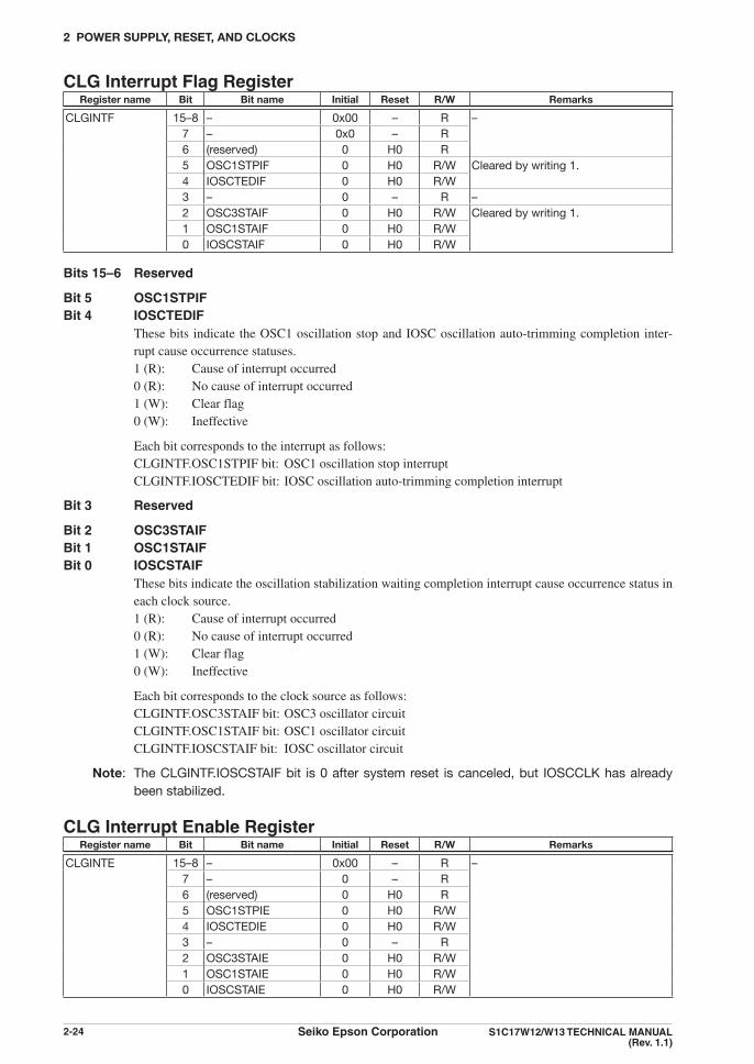
2 POWER SUPPLY, RESET, AND CLOCKS
2-24 Seiko Epson Corporation S1C17W12/W13 TECHNICAL MANUAL (Rev. 1.1)
CLG Interrupt Flag RegisterRegister name Bit Bit name Initial Reset R/W Remarks
CLGINTF 15–8 – 0x00 – R –7 – 0x0 – R6 (reserved) 0 H0 R5 OSC1STPIF 0 H0 R/W Cleared by writing 1.4 IOSCTEDIF 0 H0 R/W3 – 0 – R –2 OSC3STAIF 0 H0 R/W Cleared by writing 1.1 OSC1STAIF 0 H0 R/W0 IOSCSTAIF 0 H0 R/W
Bits 15–6 Reserved
Bit 5 OSC1STPIFBit 4 IOSCTEDIF These bits indicate the OSC1 oscillation stop and IOSC oscillation auto-trimming completion inter-
rupt cause occurrence statuses. 1 (R): Cause of interrupt occurred 0 (R): No cause of interrupt occurred 1 (W): Clear flag 0 (W): Ineffective
Each bit corresponds to the interrupt as follows: CLGINTF.OSC1STPIF bit: OSC1 oscillation stop interrupt CLGINTF.IOSCTEDIF bit: IOSC oscillation auto-trimming completion interrupt
Bit 3 Reserved
Bit 2 OSC3STAIFBit 1 OSC1STAIFBit 0 IOSCSTAIF These bits indicate the oscillation stabilization waiting completion interrupt cause occurrence status in
each clock source. 1 (R): Cause of interrupt occurred 0 (R): No cause of interrupt occurred 1 (W): Clear flag 0 (W): Ineffective
Each bit corresponds to the clock source as follows: CLGINTF.OSC3STAIF bit: OSC3 oscillator circuit CLGINTF.OSC1STAIF bit: OSC1 oscillator circuit CLGINTF.IOSCSTAIF bit: IOSC oscillator circuit
Note: The CLGINTF.IOSCSTAIF bit is 0 after system reset is canceled, but IOSCCLK has already been stabilized.
CLG Interrupt Enable RegisterRegister name Bit Bit name Initial Reset R/W Remarks
CLGINTE 15–8 – 0x00 – R –7 – 0 – R6 (reserved) 0 H0 R5 OSC1STPIE 0 H0 R/W4 IOSCTEDIE 0 H0 R/W3 – 0 – R2 OSC3STAIE 0 H0 R/W1 OSC1STAIE 0 H0 R/W0 IOSCSTAIE 0 H0 R/W

2 POWER SUPPLY, RESET, AND CLOCKS
S1C17W12/W13 TECHNICAL MANUAL Seiko Epson Corporation 2-25(Rev. 1.1)
Bits 15–6 Reserved
Bit 5 OSC1STPIEBit 4 IOSCTEDIE These bits enable the OSC1 oscillation stop and IOSC oscillation auto-trimming completion inter-
rupts. 1 (R/W): Enable interrupts 0 (R/W): Disable interrupts
Each bit corresponds to the interrupt as follows: CLGINTE.OSC1STPIE bit: OSC1 oscillation stop interrupt CLGINTE.IOSCTEDIE bit: IOSC oscillation auto-trimming completion interrupt
Bit 3 Reserved
Bit 2 OSC3STAIEBit 1 OSC1STAIEBit 0 IOSCSTAIE These bits enable the oscillation stabilization waiting completion interrupt of each clock source. 1 (R/W): Enable interrupts 0 (R/W): Disable interrupts
Each bit corresponds to the clock source as follows: CLGINTE.OSC3STAIE bit: OSC3 oscillator circuit CLGINTE.OSC1STAIE bit: OSC1 oscillator circuit CLGINTE.IOSCSTAIE bit: IOSC oscillator circuit
CLG FOUT Control RegisterRegister name Bit Bit name Initial Reset R/W Remarks
CLGFOUT 15–8 – 0x00 – R –7 – 0 – R
6–4 FOUTDIV[2:0] 0x0 H0 R/W3–2 FOUTSRC[1:0] 0x0 H0 R/W1 – 0 – R0 FOUTEN 0 H0 R/W
Bits 15–7 Reserved
Bits 6–4 FOUTDIV[2:0] These bits set the FOUT clock division ratio.
Bits 3–2 FOUTSRC[1:0] These bits select the FOUT clock source.
Table 2.6.13 FOUT Clock Source and Division Ratio Settings
CLGFOUT.FOUTDIV[2:0] bits
CLGFOUT.FOUTSRC[1:0] bits0x0 0x1 0x2 0x3
IOSCCLK OSC1CLK OSC3CLK SYSCLK0x7 1/128 1/32,768 1/128 Reserved0x6 1/64 1/4,096 1/64 Reserved0x5 1/32 1/1,024 1/32 Reserved0x4 1/16 1/256 1/16 Reserved0x3 1/8 1/8 1/8 Reserved0x2 1/4 1/4 1/4 Reserved0x1 1/2 1/2 1/2 Reserved0x0 1/1 1/1 1/1 1/1
Note: When the CLGFOUT.FOUTSRC[1:0] bits are set to 0x3, the FOUT output will be stopped in SLEEP/HALT mode as SYSCLK is stopped.
Bit 1 Reserved

2 POWER SUPPLY, RESET, AND CLOCKS
2-26 Seiko Epson Corporation S1C17W12/W13 TECHNICAL MANUAL (Rev. 1.1)
Bit 0 FOUTEN This bit controls the FOUT clock external output. 1 (R/W): Enable external output 0 (R/W): Disable external output
Note: Since the FOUT signal generated is out of sync with writings to the CLGFOUT.FOUTEN bit, a glitch may occur when the FOUT output is enabled or disabled.
CLG Oscillation Frequency Trimming RegisterRegister name Bit Bit name Initial Reset R/W Remarks
CLGTRIM 15–13 – 0x0 – R –12–8 OSC3AJ[4:0] * H0 R/WP * Determined by factory adjustment.7–6 – 0x0 – R –5–0 IOSCAJ[5:0] * H0 R/WP * Determined by factory adjustment.
Bits 15–13 Reserved
Bits 12–8 OSC3AJ[4:0] These bits sets the frequency trimming value for the OSC3 internal oscillator circuit. This setting affects all the frequencies from 250 kHz to 4 MHz.
Table 2.6.14 Frequency Trimming Setting of OSC3 Internal Oscillator CircuitCLGTRIM.OSC3AJ[4:0] bits OSC3 internal oscillator frequency
0x1f High: :
0x00 Low
Bits 7–6 Reserved
Bits 5–0 IOSCAJ[5:0] These bits sets the frequency trimming value for the IOSC internal oscillator circuit.
Table 2.6.15 Frequency Trimming Setting of IOSC Internal Oscillator CircuitCLGTRIM.IOSCAJ[5:0] bits IOSC internal oscillator frequency
0x3f High: :
0x00 Low
Note: The initial values of the CLGTRIM.OSC3AJ[4:0] and CLGTRIM.IOSCAJ[5:0] bits were adjusted so that the OSC3 and IOSC oscillator circuit characteristics described in the “Electrical Character-istics” chapter can be guaranteed. Be aware that the frequency characteristics may not be sat-isfied when these settings are altered. When altering these settings, always make sure that the relevant oscillator circuit is inactive.

3 CPU AND DEBUGGER
S1C17W12/W13 TECHNICAL MANUAL Seiko Epson Corporation 3-1(Rev. 1.1)
3 CPU and Debugger
3.1 OverviewThis IC incorporates the Seiko Epson original 16-bit CPU core (S1C17) with a debugger. The main features of the CPU core are listed below.
• Seiko Epson original 16-bit RISC processor- 24-bit general-purpose registers: 8- 24-bit special registers: 2- 8-bit special register: 1- Up to 16M bytes of memory space (24-bit address)- Harvard architecture using separated instruction bus and data bus
• Compact and fast instruction set optimized for development in C language- Code length: 16-bit fixed length- Number of instructions: 111 basic instructions (184 including variations)- Execution cycle: Main instructions are executed in one cycle.- Extended immediate instructions: Immediate data can be extended up to 24 bits.
• Supports reset, NMI, address misaligned, debug, and external interrupts.- Reads a vector from the vector table and branches to the interrupt handler routine directly.- Can generate software interrupts with a vector number specified (all vector numbers specifiable).
• HALT mode (halt instruction) and SLEEP mode (slp instruction) are provided as the standby function.
• Incorporates a debugger with three-wire communication interface to assist in software development.
Interruptcontroller
Flashmemory
Interrupt requestInterrupt levelVector number
Instruction bus
RAM RAM bus
Debugger
Bus controller
Internal bus
General-purpose registers
CPU core (S1C17)
Bit 23 Bit 0
R7
Processor status register
IL[2:0] (Bits [7:5]): Interrupt LevelIE (Bit 4): Interrupt EnableC (Bit 3): CarryV (Bit 2): OverflowZ (Bit 1): ZeroN (Bit 0): Negative
NMI
SYSCLK
DCLKDSIODST2
Bit 7 Bit 0
PSR
Special registers
Program counterBit 23 Bit 0
PC
Stack pointerBit 23 Bit 0
SP
R6R5R4R3R2R1R0
Figure 3.1.1 S1C17 Configuration

3 CPU AND DEBUGGER
3-2 Seiko Epson Corporation S1C17W12/W13 TECHNICAL MANUAL (Rev. 1.1)
3.2 CPU Core
3.2.1 CPU RegistersThe CPU includes eight general-purpose registers and three special registers (Table 3.2.1.1).
Table 3.2.1.1 Initialization of CPU RegistersCPU register name Initial Reset
General-purpose registers R0 to R7 0x000000 H0Special registers
Program counter PC The reset vector is automatically loaded. H0Stack pointer SP 0x000000 H0Processor status register PSR 0x00 H0
For details on the CPU registers, refer to the “S1C17 Family S1C17 Core Manual.” For more information on the reset vector, refer to the “Interrupt Controller” chapter.
3.2.2 Instruction SetThe CPU instruction codes are all fixed to 16 bits in length which, combined with pipelined processing, allows the most important instructions to be executed in one cycle. For details on the instructions, refer to the “S1C17 Family S1C17 Core Manual.”
3.2.3 Reading PSRThe PSR contents can be read through the MSCPSR register. Note, however, that data cannot be written to PSR through the MSCPSR register.
3.2.4 I/O Area Reserved for the S1C17 CoreThe address range from 0xfffc00 to 0xffffff is the I/O area reserved for the S1C17 core. Do not access this area ex-cept when it is required.
3.3 Debugger
3.3.1 Debugging FunctionsThe debugger provides the following functions:
• Instruction break: A debug interrupt is generated immediately before the set instruction address is executed. An instruction break can be set at up to four addresses.
• Single step: A debug interrupt is generated after each instruction has been executed.
• Forcible break: A debug interrupt is generated using an external input signal.
• Software break: A debug interrupt is generated when the brk instruction is executed.
When a debug interrupt occurs, the CPU enters DEBUG mode. The peripheral circuit operations in DEBUG mode depend on the setting of the DBRUN bit provided in the clock control register of each peripheral circuit. For more information on the DBRUN bit, refer to “Clock Supply in DEBUG Mode” in each peripheral circuit chapter. DE-BUG mode continues until a cancel command is sent from the personal computer or the CPU executes the retd in-struction. Neither hardware interrupts nor NMI are accepted during DEBUG mode.
3.3.2 Resource Requirements and Debugging ToolsDebugging work area Debugging requires a 64-byte debugging work area. For more information on the work area location, refer to
the “Memory and Bus” chapter. The start address of this debugging work area can be read from the DBRAM register.

3 CPU AND DEBUGGER
S1C17W12/W13 TECHNICAL MANUAL Seiko Epson Corporation 3-3(Rev. 1.1)
Debugging tools To perform debugging, connect ICDmini (S5U1C17001H) to the input/output pin for the debugger embedded
in this IC and control it from the personal computer. This requires the tools shown below.
• S1C17 Family In-Circuit Debugger ICDmini (S5U1C17001H)
• S1C17 Family C Compiler Package (e.g., S5U1C17001C)
3.3.3 List of debugger input/output pinsTable 3.3.3.1 lists the debug pins.
Table 3.3.3.1 List of Debug PinsPin name I/O Initial state Function
DCLK O O On-chip debugger clock output pinOutputs a clock to the ICDmini (S5U1C17001H).
DSIO I/O I On-chip debugger data input/output pinUsed to input/output debugging data and input the break signal.
DST2 O O On-chip debugger status output pinOutputs the processor status during debugging.
The debugger input/output pins are shared with general-purpose I/O ports and are initially set as the debug pins. If the debugging function is not used, these pins can be switched to general-purpose I/O port pins. For details, refer to the “I/O Ports” chapter.
Note: Do not drive the DCLK pin with a high level from outside (e.g. pulling up with a resistor). Also, do not connect (short-circuit) between the DCLK pin and another GPIO port. In the both cases, the IC may not start up normally due to unstable pin input/output status at power on.
3.3.4 External ConnectionFigure 3.3.4.1 shows a connection example between this IC and ICDmini when performing debugging.
DCLK
DSIODST2
DCLK
DSIODST2
VDD ICDmini(S5U1C17001H)
S1C17RDBG
Figure 3.3.4.1 External Connection
For the recommended pull-up resistor value, refer to “Recommended Operating Conditions, DSIO pull-up resis-tor RDBG” in the “Electrical Characteristics” chapter. RDBG is not required when using the DSIO pin as a general-purpose I/O port pin.
3.3.5 Flash Security FunctionThis IC provides a security function to protect the internal Flash memory from unauthorized reading and tampering by using the debugger through ICDmini. Figure 3.3.5.1 shows a Flash security function setting flow.
Development environmentGNU17 IDE
Factory shipment inspection process
UserEPSON
file.PA
Mask data file
Specify the unprotecting password.(6–12 alphanumeric characters (A–Z, a–z, 0–9))
ROM data and password are recorded.Programming with
ROM data and password
IC with protected Flash Shipment
Submission
Figure 3.3.5.1 Shipment of IC with ROM Data Programmed and Flash Security Function Setting Flow

3 CPU AND DEBUGGER
3-4 Seiko Epson Corporation S1C17W12/W13 TECHNICAL MANUAL (Rev. 1.1)
The following shows the status of the IC with protected Flash:
• The Flash memory data is undefined if it is read from the debugger.
• An error occurs if an attempt is made to program the Flash memory through ICDmini.
However, the Flash security function can be disabled by entering the unprotecting password predefined to GNU17 IDE (the security function will take effect again after a reset). For setting the password, refer to the “(S1C17 Family C Compiler Package) S5U1C17001C Manual.”
Note: Disable the Flash security function before debugging an IC with protected Flash via ICDmini. The debugging functions may not run normally if the Flash security function is enabled.
3.4 Control Register
MISC PSR RegisterRegister name Bit Bit name Initial Reset R/W Remarks
MSCPSR 15–8 – 0x00 – R –7–5 PSRIL[2:0] 0x0 H0 R4 PSRIE 0 H0 R3 PSRC 0 H0 R2 PSRV 0 H0 R1 PSRZ 0 H0 R0 PSRN 0 H0 R
Bits 15–8 Reserved
Bits 7–5 PSRIL[2:0] The value (0 to 7) of the PSR IL[2:0] (interrupt level) bits can be read out with these bits.
Bit 4 PSRIE The value (0 or 1) of the PSR IE (interrupt enable) bit can be read out with this bit.
Bit 3 PSRC The value (0 or 1) of the PSR C (carry) flag can be read out with this bit.
Bit 2 PSRV The value (0 or 1) of the PSR V (overflow) flag can be read out with this bit.
Bit 1 PSRZ The value (0 or 1) of the PSR Z (zero) flag can be read out with this bit.
Bit 0 PSRN The value (0 or 1) of the PSR N (negative) flag can be read out with this bit.
Debug RAM Base RegisterRegister name Bit Bit name Initial Reset R/W Remarks
DBRAM 31–24 – 0x00 – R –23–0 DBRAM[23:0] *1 H0 R
*1 Debugging work area start address
Bits 31–24 Reserved
Bits 23–0 DBRAM[23:0] The start address of the debugging work area (64 bytes) can be read out with these bits.

4 MEMORY AND BUS
S1C17W12/W13 TECHNICAL MANUAL Seiko Epson Corporation 4-1(Rev. 1.1)
4 Memory and Bus
4.1 OverviewThis IC supports up to 16M bytes of accessible memory space for both instructions and data.The features are listed below.
• Embedded Flash memory that supports on-board programming
• All memory and control registers are accessible in 16-bit width and one cycle.
• Write-protect function to protect system control registers
Figure 4.1.1 shows the memory map.
0xff ffff Reserved for core I/O area (1K bytes)(Device size: 32 bits)0xff fc00
0xff fbffReserved
0x01 40000x01 3fff
Flash area(48K bytes)
(Device size: 16 bits)
0x00 80000x00 7fff
Reserved0x00 78000x00 77ff
Display data RAM area (26 bytes)(Device size: 16 bits)0x00 7000
0x00 6fffReserved
0x00 60000x00 5fff
Peripheral circuit area(8K bytes)
(Device size: 16 bits)0x00 40000x00 3fff
Reserved0x00 08000x00 07ff0x00 07c0 Debug RAM area (64 bytes)0x00 07bf RAM area
(2K bytes)(Device size: 32 bits)0x00 0000
Figure 4.1.1 Memory Map
4.2 Bus Access CycleThe CPU uses the system clock for bus access operations. First, “Bus access cycle,” “Device size,” and “Access size” are defined as follows:
• Bus access cycle: One system clock period = 1 cycle
• Device size: Bit width of the memory and peripheral circuits that can be accessed in one cycle
• Access size: Access size designated by the CPU instructions (e.g., ld %rd, [%rb] → 16-bit data transfer)
Table 4.2.1 lists numbers of bus access cycles by different device size and access size. The peripheral circuits can be accessed with an 8-bit, 16-bit, or 32-bit instruction.

4 MEMORY AND BUS
4-2 Seiko Epson Corporation S1C17W12/W13 TECHNICAL MANUAL (Rev. 1.1)
Table 4.2.1 Number of Bus Access Cycles
Device size Access size Number of bus access cycles
8 bits 8 bits 116 bits 232 bits 4
16 bits 8 bits 116 bits 132 bits 2
32 bits 8 bits 116 bits 132 bits 1
Note: When data is transferred to a memory in 32-bit access, the eight high-order bits are written to the memory as 0x00 since the bit width of the S1C17 core general-purpose registers is 24 bits. Conversely when sending from a memory to a register, the eight high-order bits are ignored.
The CPU performs 32-bit access for stack operations in an interrupt handling. In this case, the CPU read/write 32-bit data that consists of the PSR value as the eight high-order bits and the return address as the 24 low-order bits. For more information, refer to the “S1C17 Family S1C17 Core Manual.”
The CPU adopts Harvard architecture that allows simultaneous processing of an instruction fetch and a data ac-cess. However, they are not performed simultaneously under one of the conditions listed below. This prolongs the instruction fetch cycle for the number of data area bus cycles.
• When the CPU executes an instruction stored in the Flash area and accesses data in the Flash area
• When the CPU executes an instruction stored in the Flash area and accesses data in the display data RAM area
• When the CPU executes an instruction stored in the internal RAM/display data RAM area and accesses data in the internal RAM/display data RAM area
4.3 Flash MemoryThe Flash memory is used to store application programs and data. Address 0x8000 in the Flash area is defined as the vector table base address by default, therefore a vector table must be located beginning from this address. For more information on the vector table, refer to “Vector Table” in the “Interrupt Controller” chapter.
4.3.1 Flash Memory PinTable 4.3.1.1 shows the Flash memory pin.
Table 4.3.1.1 Flash Memory PinPin name I/O Initial status Function
VPP P – Flash programming power supply
For the VPP voltage, refer to “Recommended Operating Conditions, Flash programming voltage VPP” in the “Elec-trical Characteristics” chapter.
Note: Always leave the VPP pin open except when programming the Flash memory.
4.3.2 Flash Bus Access Cycle SettingThere is a limit of frequency to access the Flash memory with no wait cycle, therefore, the number of bus access cycles for reading must be changed according to the system clock frequency. The number of bus access cycles for reading can be configured using the FLASHCWAIT.RDWAIT[1:0] bits. Select a setting for higher frequency than the system clock.

4 MEMORY AND BUS
S1C17W12/W13 TECHNICAL MANUAL Seiko Epson Corporation 4-3(Rev. 1.1)
4.3.3 Flash ProgrammingThe Flash memory supports on-board programming, so it can be programmed with the ROM data by using the de-bugger through an ICDmini. Figure 4.3.3.1 shows connection diagrams for on-board programming.
DCLK
DSIODST2
Flash VCC OUT
DCLK
DSIODST2
VPP
VDD ICDmini(S5U1C17001H)
S1C17RDBG
CVPP
Figure 4.3.3.1 External Connection
The VPP pin must be left open except when programming the Flash memory. However, it is not necessary to discon-nect the wire when using ICDmini to supply the VPP voltage, as ICDmini controls the power supply so that it will be supplied during Flash programming only. Be sure to connect CVPP for stabilizing the VPP voltage.For detailed information on ROM data programming method, refer to the “(S1C17 Family C Compiler Package) S5U1C17001C Manual.” The IC can also be shipped after being programmed in the factory with the ROM data developed. Should you desire to ship the IC with ROM data programmed from the factory, please contact our cus-tomer support.
Note: The Flash programming requires a 2.4 V or higher VDD voltage.
4.4 RAMThe RAM can be used to execute the instruction codes copied from another memory as well as storing variables or other data. This allows higher speed processing and lower power consumption than Flash memory.
Note: The 64 bytes at the end of the RAM is reserved as the debug RAM area. When using the debug functions under application development, do not access this area from the application program.
This area can be used for applications of mass-produced devices that do not need debugging.
The RAM size used by the application can be configured to equal or less than the implemented size using the MSCIRAMSZ.IRAMSZ[2:0] bits. For example, this function can be used to prevent creating programs that seek to access areas outside the RAM area of the target model when developing an application for a model in which the RAM size is smaller than this IC. After the limitation is applied, accessing an address outside the RAM area results in the same operation (undefined value is read out) as when a reserved area is accessed.
4.5 Display Data RAMThe embedded display data RAM is used to store display data for the LCD driver. Areas unused for display data in the display data RAM can be used as a general-purpose RAM. For specific information on the display data RAM, refer to “Display Data RAM” in the “LCD Driver” chapter.

4 MEMORY AND BUS
4-4 Seiko Epson Corporation S1C17W12/W13 TECHNICAL MANUAL (Rev. 1.1)
4.6 Peripheral Circuit Control RegistersThe control registers for the peripheral circuits are located in the 8K-byte area beginning with address 0x4000. Table 4.6.1 shows the control register map. For details of each control register, refer to “List of Peripheral Circuit Registers” in the appendix or “Control Registers” in each peripheral circuit chapter.
Table 4.6.1 Peripheral Circuit Control Register MapPeripheral circuit Address Register name
MISC registers (MISC) 0x4000 MSCPROT MISC System Protect Register0x4002 MSCIRAMSZ MISC IRAM Size Register0x4004 MSCTTBRL MISC Vector Table Address Low Register0x4006 MSCTTBRH MISC Vector Table Address High Register0x4008 MSCPSR MISC PSR Register
Power generator (PWG2) 0x4020 PWGCTL PWG2 Control Register0x4022 PWGTIM PWG2 Timing Control Register0x4024 PWGINTF PWG2 Interrupt Flag Register0x4026 PWGINTE PWG2 Interrupt Enable Register
Clock generator (CLG) 0x4040 CLGSCLK CLG System Clock Control Register0x4042 CLGOSC CLG Oscillation Control Register0x4044 CLGIOSC CLG IOSC Control Register0x4046 CLGOSC1 CLG OSC1 Control Register0x4048 CLGOSC3 CLG OSC3 Control Register0x404c CLGINTF CLG Interrupt Flag Register0x404e CLGINTE CLG Interrupt Enable Register0x4050 CLGFOUT CLG FOUT Control Register0x4052 CLGTRIM CLG Oscillation Frequency Trimming Register
Interrupt controller (ITC) 0x4080 ITCLV0 ITC Interrupt Level Setup Register 00x4082 ITCLV1 ITC Interrupt Level Setup Register 10x4084 ITCLV2 ITC Interrupt Level Setup Register 20x4086 ITCLV3 ITC Interrupt Level Setup Register 30x4088 ITCLV4 ITC Interrupt Level Setup Register 40x408a ITCLV5 ITC Interrupt Level Setup Register 50x408c ITCLV6 ITC Interrupt Level Setup Register 60x408e ITCLV7 ITC Interrupt Level Setup Register 70x4090 ITCLV8 ITC Interrupt Level Setup Register 8
Watchdog timer (WDT2) 0x40a0 WDTCLK WDT2 Clock Control Register0x40a2 WDTCTL WDT2 Control Register0x40a4 WDTCMP WDT2 Counter Compare Match Register
Real-time clock (RTCA) 0x40c0 RTCCTL RTC Control Register0x40c2 RTCALM1 RTC Second Alarm Register0x40c4 RTCALM2 RTC Hour/Minute Alarm Register0x40c6 RTCSWCTL RTC Stopwatch Control Register0x40c8 RTCSEC RTC Second/1Hz Register0x40ca RTCHUR RTC Hour/Minute Register0x40cc RTCMON RTC Month/Day Register0x40ce RTCYAR RTC Year/Week Register0x40d0 RTCINTF RTC Interrupt Flag Register0x40d2 RTCINTE RTC Interrupt Enable Register
Supply voltage detector (SVD) 0x4100 SVDCLK SVD Clock Control Register0x4102 SVDCTL SVD Control Register0x4104 SVDINTF SVD Status and Interrupt Flag Register0x4106 SVDINTE SVD Interrupt Enable Register
16-bit timer (T16) Ch.0 0x4160 T16_0CLK T16 Ch.0 Clock Control Register0x4162 T16_0MOD T16 Ch.0 Mode Register0x4164 T16_0CTL T16 Ch.0 Control Register0x4166 T16_0TR T16 Ch.0 Reload Data Register0x4168 T16_0TC T16 Ch.0 Counter Data Register0x416a T16_0INTF T16 Ch.0 Interrupt Flag Register0x416c T16_0INTE T16 Ch.0 Interrupt Enable Register
Flash controller (FLASHC) 0x41b0 FLASHCWAIT FLASHC Flash Read Cycle RegisterI/O ports (PPORT) 0x4200 P0DAT P0 Port Data Register
0x4202 P0IOEN P0 Port Enable Register

4 MEMORY AND BUS
S1C17W12/W13 TECHNICAL MANUAL Seiko Epson Corporation 4-5(Rev. 1.1)
Peripheral circuit Address Register nameI/O ports (PPORT) 0x4204 P0RCTL P0 Port Pull-up/down Control Register
0x4206 P0INTF P0 Port Interrupt Flag Register0x4208 P0INTCTL P0 Port Interrupt Control Register0x420a P0CHATEN P0 Port Chattering Filter Enable Register0x420c P0MODSEL P0 Port Mode Select Register0x420e P0FNCSEL P0 Port Function Select Register0x4210 P1DAT P1 Port Data Register0x4212 P1IOEN P1 Port Enable Register0x4214 P1RCTL P1 Port Pull-up/down Control Register0x4216 P1INTF P1 Port Interrupt Flag Register0x4218 P1INTCTL P1 Port Interrupt Control Register0x421a P1CHATEN P1 Port Chattering Filter Enable Register0x421c P1MODSEL P1 Port Mode Select Register0x421e P1FNCSEL P1 Port Function Select Register0x4220 P2DAT P2 Port Data Register0x4222 P2IOEN P2 Port Enable Register0x4224 P2RCTL P2 Port Pull-up/down Control Register0x4226 P2INTF P2 Port Interrupt Flag Register0x4228 P2INTCTL P2 Port Interrupt Control Register0x422a P2CHATEN P2 Port Chattering Filter Enable Register0x422c P2MODSEL P2 Port Mode Select Register0x422e P2FNCSEL P2 Port Function Select Register0x4230 P3DAT P3 Port Data Register *2, *3
0x4232 P3IOEN P3 Port Enable Register *2, *3
0x423c P3MODSEL P3 Port Mode Select Register *2, *3
0x423e P3FNCSEL P3 Port Function Select Register *2, *3
0x4240 P4DAT P4 Port Data Register *1, *2, *3
0x4242 P4IOEN P4 Port Enable Register *1, *2, *3
0x4244 P4RCTL P4 Port Pull-up/down Control Register *1, *2, *3
0x4246 P4INTF P4 Port Interrupt Flag Register *1, *2, *3
0x4248 P4INTCTL P4 Port Interrupt Control Register *1, *2, *3
0x424a P4CHATEN P4 Port Chattering Filter Enable Register *1, *2, *3
0x424c P4MODSEL P4 Port Mode Select Register *1, *2, *3
0x424e P4FNCSEL P4 Port Function Select Register *1, *2, *3
0x42d0 PDDAT Pd Port Data Register0x42d2 PDIOEN Pd Port Enable Register0x42d4 PDRCTL Pd Port Pull-up/down Control Register0x42dc PDMODSEL Pd Port Mode Select Register0x42de PDFNCSEL Pd Port Function Select Register0x42e0 PCLK P Port Clock Control Register0x42e2 PINTFGRP P Port Interrupt Flag Group Register
Universal port multiplexer (UPMUX)
0x4300 P0UPMUX0 P00–01 Universal Port Multiplexer Setting Register0x4302 P0UPMUX1 P02–03 Universal Port Multiplexer Setting Register0x4304 P0UPMUX2 P04–05 Universal Port Multiplexer Setting Register0x4306 P0UPMUX3 P06–07 Universal Port Multiplexer Setting Register0x4308 P1UPMUX0 P10–11 Universal Port Multiplexer Setting Register0x430a P1UPMUX1 P12–13 Universal Port Multiplexer Setting Register0x430c P1UPMUX2 P14–15 Universal Port Multiplexer Setting Register0x430e P1UPMUX3 P16–17 Universal Port Multiplexer Setting Register0x4310 P2UPMUX0 P20–21 Universal Port Multiplexer Setting Register0x4312 P2UPMUX1 P22–23 Universal Port Multiplexer Setting Register0x4314 P2UPMUX2 P24–25 Universal Port Multiplexer Setting Register0x4316 P2UPMUX3 P26 Universal Port Multiplexer Setting Register
UART (UART2) Ch.0 0x4380 UA0CLK UART2 Ch.0 Clock Control Register0x4382 UA0MOD UART2 Ch.0 Mode Register0x4384 UA0BR UART2 Ch.0 Baud-Rate Register0x4386 UA0CTL UART2 Ch.0 Control Register0x4388 UA0TXD UART2 Ch.0 Transmit Data Register0x438a UA0RXD UART2 Ch.0 Receive Data Register0x438c UA0INTF UART2 Ch.0 Status and Interrupt Flag Register0x438e UA0INTE UART2 Ch.0 Interrupt Enable Register

4 MEMORY AND BUS
4-6 Seiko Epson Corporation S1C17W12/W13 TECHNICAL MANUAL (Rev. 1.1)
Peripheral circuit Address Register name16-bit timer (T16) Ch.1 0x43a0 T16_1CLK T16 Ch.1 Clock Control Register
0x43a2 T16_1MOD T16 Ch.1 Mode Register0x43a4 T16_1CTL T16 Ch.1 Control Register0x43a6 T16_1TR T16 Ch.1 Reload Data Register0x43a8 T16_1TC T16 Ch.1 Counter Data Register0x43aa T16_1INTF T16 Ch.1 Interrupt Flag Register0x43ac T16_1INTE T16 Ch.1 Interrupt Enable Register
Synchronous serial interface (SPIA) Ch.0
0x43b0 SPI0MOD SPIA Ch.0 Mode Register0x43b2 SPI0CTL SPIA Ch.0 Control Register0x43b4 SPI0TXD SPIA Ch.0 Transmit Data Register0x43b6 SPI0RXD SPIA Ch.0 Receive Data Register0x43b8 SPI0INTF SPIA Ch.0 Interrupt Flag Register0x43ba SPI0INTE SPIA Ch.0 Interrupt Enable Register
I2C (I2C) Ch.0 0x43c0 I2C0CLK I2C Ch.0 Clock Control Register0x43c2 I2C0MOD I2C Ch.0 Mode Register0x43c4 I2C0BR I2C Ch.0 Baud-Rate Register0x43c8 I2C0OADR I2C Ch.0 Own Address Register0x43ca I2C0CTL I2C Ch.0 Control Register0x43cc I2C0TXD I2C Ch.0 Transmit Data Register0x43ce I2C0RXD I2C Ch.0 Receive Data Register0x43d0 I2C0INTF I2C Ch.0 Status and Interrupt Flag Register0x43d2 I2C0INTE I2C Ch.0 Interrupt Enable Register
16-bit PWM timer (T16B) Ch.0 0x5000 T16B0CLK T16B Ch.0 Clock Control Register0x5002 T16B0CTL T16B Ch.0 Counter Control Register0x5004 T16B0MC T16B Ch.0 Max Counter Data Register0x5006 T16B0TC T16B Ch.0 Timer Counter Data Register0x5008 T16B0CS T16B Ch.0 Counter Status Register0x500a T16B0INTF T16B Ch.0 Interrupt Flag Register0x500c T16B0INTE T16B Ch.0 Interrupt Enable Register0x5010 T16B0CCCTL0 T16B Ch.0 Compare/Capture 0 Control Register0x5012 T16B0CCR0 T16B Ch.0 Compare/Capture 0 Data Register0x5018 T16B0CCCTL1 T16B Ch.0 Compare/Capture 1 Control Register0x501a T16B0CCR1 T16B Ch.0 Compare/Capture 1 Data Register
16-bit PWM timer (T16B) Ch.1 0x5040 T16B1CLK T16B Ch.1 Clock Control Register0x5042 T16B1CTL T16B Ch.1 Counter Control Register0x5044 T16B1MC T16B Ch.1 Max Counter Data Register0x5046 T16B1TC T16B Ch.1 Timer Counter Data Register0x5048 T16B1CS T16B Ch.1 Counter Status Register0x504a T16B1INTF T16B Ch.1 Interrupt Flag Register0x504c T16B1INTE T16B Ch.1 Interrupt Enable Register0x5050 T16B1CCCTL0 T16B Ch.1 Compare/Capture 0 Control Register0x5052 T16B1CCR0 T16B Ch.1 Compare/Capture 0 Data Register0x5058 T16B1CCCTL1 T16B Ch.1 Compare/Capture 1 Control Register0x505a T16B1CCR1 T16B Ch.1 Compare/Capture 1 Data Register
UART (UART2) Ch.1 0x5200 UA1CLK UART2 Ch.1 Clock Control Register0x5202 UA1MOD UART2 Ch.1 Mode Register0x5204 UA1BR UART2 Ch.1 Baud-Rate Register0x5206 UA1CTL UART2 Ch.1 Control Register0x5208 UA1TXD UART2 Ch.1 Transmit Data Register0x520a UA1RXD UART2 Ch.1 Receive Data Register0x520c UA1INTF UART2 Ch.1 Status and Interrupt Flag Register0x520e UA1INTE UART2 Ch.1 Interrupt Enable Register
16-bit timer (T16) Ch.2 0x5260 T16_2CLK T16 Ch.2 Clock Control Register0x5262 T16_2MOD T16 Ch.2 Mode Register0x5264 T16_2CTL T16 Ch.2 Control Register0x5266 T16_2TR T16 Ch.2 Reload Data Register0x5268 T16_2TC T16 Ch.2 Counter Data Register0x526a T16_2INTF T16 Ch.2 Interrupt Flag Register0x526c T16_2INTE T16 Ch.2 Interrupt Enable Register

4 MEMORY AND BUS
S1C17W12/W13 TECHNICAL MANUAL Seiko Epson Corporation 4-7(Rev. 1.1)
Peripheral circuit Address Register nameSound generator (SNDA) 0x5300 SNDCLK SNDA Clock Control Register
0x5302 SNDSEL SNDA Select Register0x5304 SNDCTL SNDA Control Register0x5306 SNDDAT SNDA Data Register0x5308 SNDINTF SNDA Interrupt Flag Register0x530a SNDINTE SNDA Interrupt Enable Register
IR remote controller (REMC2) 0x5320 REMCLK REMC2 Clock Control Register0x5322 REMDBCTL REMC2 Data Bit Counter Control Register0x5324 REMDBCNT REMC2 Data Bit Counter Register0x5326 REMAPLEN REMC2 Data Bit Active Pulse Length Register0x5328 REMDBLEN REMC2 Data Bit Length Register0x532a REMINTF REMC2 Status and Interrupt Flag Register0x532c REMINTE REMC2 Interrupt Enable Register0x5330 REMCARR REMC2 Carrier Waveform Register0x5332 REMCCTL REMC2 Carrier Modulation Control Register
LCD driver (LCD4A) 0x5400 LCD4CLK LCD4A Clock Control Register0x5402 LCD4CTL LCD4A Control Register0x5404 LCD4TIM1 LCD4A Timing Control Register 10x5406 LCD4TIM2 LCD4A Timing Control Register 20x5408 LCD4PWR LCD4A Power Control Register0x540a LCD4DSP LCD4A Display Control Register0x540c LCD4COMC0 LCD4A COM Pin Control Register 00x5410 LCD4INTF LCD4A Interrupt Flag Register0x5412 LCD4INTE LCD4A Interrupt Enable Register
R/F converter (RFC) Ch.0 0x5440 RFC0CLK RFC Ch.0 Clock Control Register *3
0x5442 RFC0CTL RFC Ch.0 Control Register *3
0x5444 RFC0TRG RFC Ch.0 Oscillation Trigger Register *3
0x5446 RFC0MCL RFC Ch.0 Measurement Counter Low Register *3
0x5448 RFC0MCH RFC Ch.0 Measurement Counter High Register *3
0x544a RFC0TCL RFC Ch.0 Time Base Counter Low Register *3
0x544c RFC0TCH RFC Ch.0 Time Base Counter High Register *3
0x544e RFC0INTF RFC Ch.0 Interrupt Flag Register *3
0x5450 RFC0INTE RFC Ch.0 Interrupt Enable Register *3
*1 Not available in the S1C17W12 SQFN7-48pin package*2 Not available in the S1C17W13 SQFN7-48pin package*3 Not available in the S1C17W13 TQFP12-48pin package
4.6.1 System-Protect FunctionThe system-protect function protects control registers and bits from writings. They cannot be rewritten unless write protection is removed by writing 0x0096 to the MSCPROT.PROT[15:0] bits. This function is provided to prevent deadlock that may occur when a system-related register is altered by a runaway CPU. See “Control Registers” in each peripheral circuit to identify the registers and bits with write protection.
Note: Once write protection is removed using the MSCPROT.PROT[15:0] bits, write enabled status is maintained until write protection is applied again. After the registers/bits required have been al-tered, apply write protection.
4.7 Control Registers
MISC System Protect RegisterRegister name Bit Bit name Initial Reset R/W Remarks
MSCPROT 15–0 PROT[15:0] 0x0000 H0 R/W –
Bits 15–0 PROT[15:0] These bits protect the control registers related to the system against writings. 0x0096 (R/W): Disable system protection Other than 0x0096 (R/W): Enable system protection

4 MEMORY AND BUS
4-8 Seiko Epson Corporation S1C17W12/W13 TECHNICAL MANUAL (Rev. 1.1)
While the system protection is enabled, any data will not be written to the affected control bits (bits with “WP” or “R/WP” appearing in the R/W column).
MISC IRAM Size RegisterRegister name Bit Bit name Initial Reset R/W Remarks
MSCIRAMSZ 15–9 – 0x00 – R –8 (reserved) 0 H0 R/WP Always set to 0.
7–3 – 0x04 – R –2–0 IRAMSZ[2:0] 0x2 H0 R/WP
Bits 15–3 Reserved
Bits 2–0 IRAMSZ[2:0] These bits set the internal RAM size that can be used.
Table 4.7.1 Internal RAM Size SelectionsMSCIRAMSZ.IRAMSZ[2:0] bits Internal RAM size
0x7–0x3 Reserved0x2 2KB0x1 1KB0x0 512B
FLASHC Flash Read Cycle RegisterRegister name Bit Bit name Initial Reset R/W Remarks
FLASHCWAIT 15–9 – 0x00 – R –8 (reserved) 1 H0 R/WP Always set to 1.
7–2 – 0x00 – R –1–0 RDWAIT[1:0] 0x1 H0 R/WP
Bits 15–2 Reserved
Bits 1–0 RDWAIT[1:0] These bits set the number of bus access cycles for reading from the Flash memory.
Table 4.7.2 Setting Number of Bus Access Cycles for Flash Read When VDD = 1.2 to 1.6 V
FLASHCWAIT.RDWAIT[1:0] bits Number of bus Access cycles System clock frequency0x3 4 1.1 MHz (max.)0x2 3 1.1 MHz (max.)0x1 2 1.1 MHz (max.)0x0 1 800 kHz (max.)
When VDD = 1.6 to 3.6 VFLASHCWAIT.RDWAIT[1:0] bits Number of bus Access cycles System clock frequency
0x3 4 4.2 MHz (max.)0x2 3 4.2 MHz (max.)0x1 2 4.2 MHz (max.)0x0 1 2.1 MHz (max.)
Note: Be sure to set the FLASHCWAIT.RDWAIT[1:0] bits before the system clock is configured.

5 INTERRUPT CONTROLLER (ITC)
S1C17W12/W13 TECHNICAL MANUAL Seiko Epson Corporation 5-1(Rev. 1.1)
5 Interrupt Controller (ITC)
5.1 OverviewThe features of the ITC are listed below.
• Honors interrupt requests from the peripheral circuits and outputs the interrupt request, interrupt level and vector number signals to the CPU.
• The interrupt level of each interrupt source is selectable from among eight levels.
• Priorities of the simultaneously generated interrupts are established from the interrupt level.
• Handles the simultaneously generated interrupts with the same interrupt level as smaller vector number has high-er priority.
Figure 5.1.1 shows the configuration of the ITC.
CPU core
ITC
Watchdog timer
Interrupt request
Interrupt level
Vector number
Internal reset signalDebug interruptHALT/SLEEP
cancelation signal
Interrupt request
NMI
ILVx[2:0]
Interruptcontrolcircuit
ILVy[2:0]Interrupt request
• •
•
• •
•
Peripheral circuit
Peripheral circuit
Inte
rnal
dat
a bu
s
Figure 5.1.1 ITC Configuration
5.2 Vector TableThe vector table contains the vectors to the interrupt handler routines (handler routine start address) that will be read by the CPU to execute the handler when an interrupt occurs. Table 5.2.1 shows the vector table.
Table 5.2.1 Vector TableTTBR initial value = 0x8000
Vector number/Software interrupt
numberVector address Hardware interrupt name Cause of hardware interrupt Priority
0 (0x00) TTBR + 0x00 Reset • Low input to the #RESET pin• Power-on reset• Key reset• Watchdog timer overflow *2
• Supply voltage detector reset
1
1 (0x01) TTBR + 0x04 Address misaligned interrupt Memory access instruction 2– (0xfffc00) Debugging interrupt brk instruction, etc. 3
2 (0x02) TTBR + 0x08 NMI Watchdog timer overflow *2 43 (0x03) TTBR + 0x0c Reserved for C compiler – –

5 INTERRUPT CONTROLLER (ITC)
5-2 Seiko Epson Corporation S1C17W12/W13 TECHNICAL MANUAL (Rev. 1.1)
Vector number/Software interrupt
numberVector address Hardware interrupt name Hardware interrupt flag Priority
4 (0x04) TTBR + 0x10 Supply voltage detector interrupt
Low power supply voltage detection High *1
↑5 (0x05) TTBR + 0x14 Port interrupt Port input6 (0x06) TTBR + 0x18 Power generator interrupt PWG2 mode transition completion7 (0x07) TTBR + 0x1c Clock generator interrupt • IOSC oscillation stabilization waiting completion
• OSC1 oscillation stabilization waiting completion• OSC3 oscillation stabilization waiting completion• OSC1 oscillation stop• IOSC oscillation auto-trimming completion
8 (0x08) TTBR + 0x20 Real-time clock interrupt • 1-day, 1-hour, 1-minute, and 1-second• 1/32-second, 1/8-second, 1/4-second, and 1/2-second• Stopwatch 1 Hz, 10 Hz, and 100 Hz• Alarm• Theoretical regulation completion
9 (0x09) TTBR + 0x24 16-bit timer Ch.0 interrupt Underflow10 (0x0a) TTBR + 0x28 UART Ch.0 interrupt • End of transmission
• Framing error• Parity error• Overrun error• Receive buffer two bytes full• Receive buffer one byte full• Transmit buffer empty
11 (0x0b) TTBR + 0x2c 16-bit timer Ch.1 interrupt Underflow12 (0x0c) TTBR + 0x30 Synchronous serial interface
Ch.0 interrupt• End of transmission• Receive buffer full• Transmit buffer empty• Overrun error
13 (0x0d) TTBR + 0x34 I2C Ch.0 interrupt • End of data transfer• General call address reception• NACK reception• STOP condition• START condition• Error detection• Receive buffer full• Transmit buffer empty
14 (0x0e) TTBR + 0x38 16-bit PWM timer Ch.0 interrupt
• Capture overwrite• Compare/capture• Counter MAX• Counter zero
15 (0x0f) TTBR + 0x3c 16-bit PWM timer Ch.1 interrupt
• Capture overwrite• Compare/capture• Counter MAX• Counter zero
16 (0x10) TTBR + 0x40 UART Ch.1 interrupt • End of transmission• Framing error• Parity error• Overrun error• Receive buffer two bytes full• Receive buffer one byte full• Transmit buffer empty
17 (0x11) TTBR + 0x44 16-bit timer Ch.2 interrupt Underflow18 (0x12) TTBR + 0x48 Sound generator interrupt • Sound buffer empty
• Sound output completion19 (0x13) TTBR + 0x4c LCD driver interrupt Frame20 (0x14) TTBR + 0x50 R/F converter Ch.0 interrupt • Reference oscillation completion
• Sensor A oscillation completion• Sensor B oscillation completion• Measurement counter overflow error• Time base counter overflow error
21 (0x15) TTBR + 0x54 IR remote controller interrupt • Compare AP• Compare DB
22 (0x16) TTBR + 0x58 reserved –: : : : ↓
31 (0x1f) TTBR + 0x7c reserved – Low *1
*1 When the same interrupt level is set*2 Either reset or NMI can be selected as the watchdog timer interrupt with software.
5 INTERRUPT CONTROLLER (ITC)
S1C17W12/W13 TECHNICAL MANUAL Seiko Epson Corporation 5-3(Rev. 1.1)
5.2.1 Vector Table Base Address (TTBR)The MSCTTBRL and MSCTTBRH registers are provided to set the base (start) address of the vector table in which interrupt vectors are programmed. “TTBR” described in Table 5.2.1 means the value set to these registers. After an initial reset, the MSCTTBRL and MSCTTBRH registers are set to address 0x8000. Therefore, even when the vec-tor table location is changed, it is necessary that at least the reset vector be written to the above address. Bits 7 to 0 in the MSCTTBRL register are fixed at 0, so the vector table always begins from a 256-byte boundary address.
5.3 InitializationThe following shows an example of the initial setting procedure related to interrupts:
1. Execute the di instruction to set the CPU into interrupt disabled state.
2. If the vector table start address is different from the default address, set it to the MSCTTBRL and MSCTTBRH registers after removing system protection by writing 0x0096 to the MSCPROT.PROT[15:0] bits. Then, write a value other than 0x0096 to the MSCPROT.PROT[15:0] bits to set system protection.
3. Set the interrupt enable bit of the peripheral circuit to 0 (interrupt disabled).
4. Set the interrupt level for the peripheral circuit using the ITCLVx.ILVx[2:0] bits in the ITC.
5. Configure the peripheral circuit and start its operation.
6. Clear the interrupt factor flag of the peripheral circuit.
7. Set the interrupt enable bit of the peripheral circuit to 1 (interrupt enabled).
8. Execute the ei instruction to set the CPU into interrupt enabled state.
5.4 Maskable Interrupt Control and Operations
5.4.1 Peripheral Circuit Interrupt ControlThe peripheral circuit that generates interrupts includes an interrupt enable bit and an interrupt flag for each inter-rupt cause.
Interrupt flag: The flag is set to 1 when the interrupt cause occurs. The clear condition depends on the periph-eral circuit.
Interrupt enable bit: By setting this bit to 1 (interrupt enabled), an interrupt request will be sent to the ITC when the interrupt flag is set to 1. When this bit is set to 0 (interrupt disabled), no interrupt request will be sent to the ITC even if the interrupt flag is set to 1. An interrupt request is also sent to the ITC if the status is changed to interrupt enabled when the interrupt flag is 1.
For specific information on causes of interrupts, interrupt flags, and interrupt enable bits, refer to the respective pe-ripheral circuit descriptions.
Note: To prevent occurrence of unnecessary interrupts, the corresponding interrupt flag should be cleared before setting the interrupt enable bit to 1 (interrupt enabled) and before terminating the interrupt handler routine.
5.4.2 ITC Interrupt Request ProcessingOn receiving an interrupt signal from a peripheral circuit, the ITC sends an interrupt request, the interrupt level, and the vector number to the CPU. Vector numbers are determined by the ITC internal hardware for each interrupt cause, as shown in Table 5.2.1. The interrupt level is a value to configure the priority, and it can be set to between 0 (low) and 7 (high) using the ITCLVx.ILVx[2:0] bits provided for each interrupt source. The default ITC settings are level 0 for all maskable interrupts. Interrupt requests are not accepted by the CPU if the level is 0.
The ITC outputs the interrupt request with the highest priority to the CPU in accordance with the following condi-tions if interrupt requests are input to the ITC simultaneously from two or more peripheral circuits.
• The interrupt with the highest interrupt level takes precedence.
• If multiple interrupt requests are input with the same interrupt level, the interrupt with the lowest vector number takes precedence.

5 INTERRUPT CONTROLLER (ITC)
5-4 Seiko Epson Corporation S1C17W12/W13 TECHNICAL MANUAL (Rev. 1.1)
The other interrupts occurring at the same time are held until all interrupts with higher priority levels have been ac-cepted by the CPU.If an interrupt cause with higher priority occurs while the ITC is outputting an interrupt request signal to the CPU (before being accepted by the CPU), the ITC alters the vector number and interrupt level signals to the setting in-formation on the more recent interrupt. The previously occurring interrupt is held. The held interrupt is canceled and no interrupt is generated if the interrupt flag in the peripheral circuit is cleared via software.
Note: Before changing the interrupt level, make sure that no interrupt of which the level is changed can be generated (the interrupt enable bit of the peripheral circuit is set to 0 or the peripheral circuit is deactivated).
5.4.3 Conditions to Accept Interrupt Requests by the CPUThe CPU accepts an interrupt request sent from the ITC when all of the following conditions are met:
• The IE (Interrupt Enable) bit of the PSR has been set to 1.
• The interrupt request that has occurred has a higher interrupt level than the value set in the IL[2:0] (Interrupt Level) bits of the PSR.
• No other interrupt request having higher priority, such as NMI, has occurred.
5.5 NMIThe watchdog timer embedded in this IC can generate a non-maskable interrupt (NMI). This interrupt takes prece-dence over other interrupts and is unconditionally accepted by the CPU. For detailed information on generating NMI, refer to the “Watchdog Timer” chapter.
5.6 Software InterruptsThe CPU provides the “int imm5” and “intl imm5, imm3” instructions allowing the software to generate any inter-rupts. The operand imm5 specifies a vector number (0–31) in the vector table. In addition to this, the intl instruction has the operand imm3 to specify the interrupt level (0–7) to be set to the IL[2:0] bits in the PSR. The software inter-rupt cannot be disabled (non-maskable interrupt). The processor performs the same interrupt processing operation as that of the hardware interrupt.
5.7 Interrupt Processing by the CPUThe CPU samples interrupt requests for each cycle. On accepting an interrupt request, the CPU switches to inter-rupt processing immediately after execution of the current instruction has been completed.Interrupt processing involves the following steps:
1. The PSR and current program counter (PC) values are saved to the stack.
2. The PSR IE bit is cleared to 0 (disabling subsequent maskable interrupts).
3. The PSR IL[2:0] bits are set to the received interrupt level. (The NMI does not affect the IL bits.)
4. The vector for the interrupt occurred is loaded to the PC to execute the interrupt handler routine.
When an interrupt is accepted, Step 2 prevents subsequent maskable interrupts. Setting the IE bit to 1 in the inter-rupt handler routine allows handling of multiple interrupts. In this case, since the IL[2:0] bits are changed by Step 3, only an interrupt with a higher level than that of the currently processed interrupt will be accepted.Ending interrupt handler routines using the reti instruction returns the PSR to the state before the interrupt occurred. The program resumes processing following the instruction being executed at the time the interrupt occurred.
Note: When HALT or SLEEP mode is canceled, the CPU jumps to the interrupt handler routine after executing one instruction. To execute the interrupt handler routine immediately after HALT or SLEEP mode is canceled, place the nop instruction at just behind the halt/slp instruction.

5 INTERRUPT CONTROLLER (ITC)
S1C17W12/W13 TECHNICAL MANUAL Seiko Epson Corporation 5-5(Rev. 1.1)
5.8 Control Registers
MISC Vector Table Address Low RegisterRegister name Bit Bit name Initial Reset R/W Remarks
MSCTTBRL 15–8 TTBR[15:8] 0x80 H0 R/WP –7–0 TTBR[7:0] 0x00 H0 R
Bits 15–0 TTBR[15:0] These bits set the vector table base address (16 low-order bits).
MISC Vector Table Address High RegisterRegister name Bit Bit name Initial Reset R/W Remarks
MSCTTBRH 15–8 – 0x00 – R –7–0 TTBR[23:16] 0x00 H0 R/WP
Bits 15–8 Reserved
Bits 7–0 TTBR[23:16] These bits set the vector table base address (eight high-order bits).
ITC Interrupt Level Setup Register xRegister name Bit Bit name Initial Reset R/W Remarks
ITCLVx 15–11 – 0x00 – R –10–8 ILVy1[2:0] 0x0 H0 R/W7–3 – 0x00 – R2–0 ILVy0[2:0] 0x0 H0 R/W
Bits 15–11 ReservedBits 7–3 Reserved
Bits 10–8 ILVy1[2:0] (y1 = 2x +1)Bits 2–0 ILVy0[2:0] (y0 = 2x) These bits set the interrupt level of each interrupt.
Table 5.8.1 Interrupt Level and Priority SettingsITCLVx.ILVy[2:0] bits Interrupt level Priority
0x7 7 High0x6 6 ↑· · · · · ·0x1 1 ↓0x0 0 Low
The following shows the ITCLVx register configuration in this IC.
Table 5.8.2 List of ITCLVx RegistersRegister name Bit Bit name Initial Reset R/W Remarks
ITCLV0(ITC Interrupt Level Setup Register 0)
15–11 – 0x00 – R –10–8 ILV1[2:0] 0x0 H0 R/W Port interrupt (ILVPPORT)7–3 – 0x00 – R –2–0 ILV0[2:0] 0x0 H0 R/W Supply voltage detector interrupt
(ILVSVD)ITCLV1(ITC Interrupt Level Setup Register 1)
15–11 – 0x00 – R –10–8 ILV3[2:0] 0x0 H0 R/W Clock generator interrupt (ILVCLG)7–3 – 0x00 – R –2–0 ILV2[2:0] 0x0 H0 R/W Power generator interrupt (ILVPWG2)
ITCLV2(ITC Interrupt Level Setup Register 2)
15–11 – 0x00 – R –10–8 ILV5[2:0] 0x0 H0 R/W 16-bit timer Ch.0 interrupt (ILVT16_0)7–3 – 0x00 – R –2–0 ILV4[2:0] 0x0 H0 R/W Real-time clock interrupt (ILVRTCA_0)

5 INTERRUPT CONTROLLER (ITC)
5-6 Seiko Epson Corporation S1C17W12/W13 TECHNICAL MANUAL (Rev. 1.1)
Register name Bit Bit name Initial Reset R/W Remarks
ITCLV3(ITC Interrupt Level Setup Register 3)
15–11 – 0x00 – R –10–8 ILV7[2:0] 0x0 H0 R/W 16-bit timer Ch.1 interrupt (ILVT16_1)7–3 – 0x00 – R –2–0 ILV6[2:0] 0x0 H0 R/W UART Ch.0 interrupt (ILVUART2_0)
ITCLV4(ITC Interrupt Level Setup Register 4)
15–11 – 0x00 – R –10–8 ILV9[2:0] 0x0 H0 R/W I2C Ch.0 interrupt (ILVI2C_0)7–3 – 0x00 – R –2–0 ILV8[2:0] 0x0 H0 R/W Synchronous serial interface Ch.0
interrupt (ILVSPIA_0)ITCLV5(ITC Interrupt Level Setup Register 5)
15–11 – 0x00 – R –10–8 ILV11[2:0] 0x0 H0 R/W 16-bit PWM timer Ch.1 interrupt
(ILVT16B_1)7–3 – 0x00 – R –2–0 ILV10[2:0] 0x0 H0 R/W 16-bit PWM timer Ch.0 interrupt
(ILVT16B_0)ITCLV6(ITC Interrupt Level Setup Register 6)
15–11 – 0x00 – R –10–8 ILV13[2:0] 0x0 H0 R/W 16-bit timer Ch.2 interrupt (ILVT16_2) 7–3 – 0x00 – R –2–0 ILV12[2:0] 0x0 H0 R/W UART Ch.1 interrupt (ILVUART2_1)
ITCLV7(ITC Interrupt Level Setup Register 7)
15–11 – 0x00 – R –10–8 ILV15[2:0] 0x0 H0 R/W LCD driver interrupt (ILVLCD4A)7–3 – 0x00 – R –2–0 ILV14[2:0] 0x0 H0 R/W Sound generator interrupt
(ILVSNDA_0)ITCLV8(ITC Interrupt Level Setup Register 8)
15–11 – 0x00 – R –10–8 ILV17[2:0] 0x0 H0 R/W IR remote controller interrupt
(ILVREMC2_0)7–3 – 0x00 – R –2–0 ILV16[2:0] 0x0 H0 R/W R/F converter Ch.0 interrupt
(ILVRFC_0)

6 I/O PORTS (PPORT)
S1C17W12/W13 TECHNICAL MANUAL Seiko Epson Corporation 6-1(Rev. 1.1)
6 I/O Ports (PPORT)
6.1 OverviewPPORT controls the I/O ports. The main features are outlined below.
• Allows software to configure the function of each port that supports general-purpose I/O (GPIO). - Each port can be configured with or without a pull-up or pull-down resistor.- Each port can be configured with or without a chattering filter.- Allows selection of the function (general-purpose I/O port (GPIO) function, up to four peripheral I/O func-
tions) to be assigned to each port.
• Provides Nch open drain LED drive pins for directly driving LEDs.
• Ports, except for those shared with debug pins, are initially placed into Hi-Z state. (No current passes through the pin during this Hi-Z state.)
Note: ‘x’, which is used in the port names Pxy, register names, and bit names, refers to a port group (x = 0, 1, 2, ··· , d) and ‘y’ refers to a port number (y = 0, 1, 2, ··· , 7).
Figure 6.1.1 shows the configuration of PPORT.
Table 6.1.1 Port Configuration of S1C17W12/W13
Item S1C17W12 S1C17W13SQFN7-48pin Chip TQFP12-48pin SQFN7-48pin QFP13-64pin/Chip
Port groups included P0 P0[7:0] (8) *1, *2 P0[7:0] (8) *1, *2 P0[6:0] (7) *1, *2 P0[7:0] (8) *1, *2 P0[7:0] (8) *1, *2
P1 P1[7:0] (8) *1, *2 P1[7:0] (8) *1, *2 P1[1:0]P1[7:3] (7) *1, *2
P1[7:0] (8) *1, *2 P1[7:0] (8) *1, *2
P2 P2[6:0] (7) *1, *2 P2[6:0] (7) *1, *2 P2[6:0] (7) *1, *2 P2[6:0] (7) *1, *2 P2[6:0] (7) *1, *2
P3 P3[1:0] (2)(LED drive pins)
P3[1:0] (2)(LED drive pins)
– (0) – (0) P3[1:0] (2)(LED drive pins)
P4 – (0) P4[3:0] (4) *1, *2 – (0) – (0) P4[3:0] (4) *1, *2
Pd Pd[2:0] (3) *1
(Pd2: output only)Pd[4:0] (5) *1
(Pd2: output only)Pd[4:0] (5) *1
(Pd2: output only)Pd[2:0] (3) *1
(Pd2: output only)Pd[4:0] (5) *1
(Pd2: output only)Total number of ports I/O port: 25
Output port: 1LED drive port: 2
I/O port: 31Output port: 1LED drive port: 2
I/O port: 25Output port: 1
I/O port: 25Output port: 1
I/O port: 31Output port: 1LED drive port: 2
Ports for debug function Pd[2:0]Key-entry reset function Supported (P0[3:0])*1 Ports with general-purpose I/O function (GPIO)*2 Ports with interrupt function

6 I/O PORTS (PPORT)
6-2 Seiko Epson Corporation S1C17W12/W13 TECHNICAL MANUAL (Rev. 1.1)
Pxy
PPORT
PxyPxy
Peripheral I/O function 0 I/O controlPeripheral I/O function 1 I/O controlPeripheral I/O function 2 I/O controlPeripheral I/O function 3 I/O control
General-purposeI/O control
GPIO function
I/O cellcontrol signal
Output signal
Input signal
PxOUTy
PxyMUX[1:0]
GPIO/peripheral I/O
function switching
circuitPxOENy
PxIENy
PxPDPUy
PxRENy
PxINy
KRSTCFG[1:0]
CLKSRC[1:0]
CLKDIV[3:0]
PxSELy
Clock generator
Interrupt controller
System reset controller
DBRUN
Pxy
CLK_PPORT
I/O cell
Inte
rnal
dat
a bu
s
Exist only in the ports that supports the interrupt function.
Chattering filter
Interrupt control circuit
Key-entry reset control
circuit
PxCHATENy
PxEDGEy
PxIFy
PxIEy
PxINT
Key-entry reset signal
Figure 6.1.1 PPORT Configuration
6.2 I/O Cell Structure and FunctionsFigure 6.2.1 shows the I/O cell Configuration.
Pull-up/downControl signal
Over voltage tolerant fail-safe type I/O cell
Input signal
Input control signal
Output signal
Output control signal
LCD/analog signal
Analog control signal
Pull-up/downControl signal
Input signal
Input control signal
Output signal
Output control signal
LCD/analog signal
Analog control signal
Pull-up/down control
Analog signal control
VDD
RINU/RIND
RINU/RIND
VDD
VDD
VSS
Pxy
VSS
Standard I/O cell
Pull-up/down control
Analog signal control
VDD
VDD
VDD
VDD
VSS
Pxy
VSS
∗ No diode is connected at the VDD side.
I/O cell for LED drive pin
Output signal
Output control signal
VDD
Pxy
VSS
VSS
Figure 6.2.1 I/O Cell Configuration

6 I/O PORTS (PPORT)
S1C17W12/W13 TECHNICAL MANUAL Seiko Epson Corporation 6-3(Rev. 1.1)
Refer to “Pin Descriptions” in the “Overview” chapter for the cell type, either the over voltage tolerant fail-safe type I/O cell or the standard I/O cell, included in each port.
6.2.1 Schmitt InputThe input functions are all configured with the Schmitt interface level. When a port is set to input disable status (PxIOEN.PxIENy bit = 0), unnecessary current is not consumed if the Pxy pin is placed into floating status.
6.2.2 Over Voltage Tolerant Fail-Safe Type I/O CellThe over voltage tolerant fail-safe type I/O cell allows interfacing without passing unnecessary current even if a voltage exceeding VDD is applied to the port. Also unnecessary current is not consumed when the port is externally biased without supplying VDD. However, be sure to avoid applying a voltage exceeding the recommended maxi-mum operating power supply voltage to the port.
6.2.3 Pull-Up/Pull-DownThe GPIO port has a pull-up/pull-down function. Either pull-up or pull-down may be selected for each port indi-vidually. This function may also be disabled for the port that does not require pulling up/down.When the port level is switched from low to high through the pull-up resistor included in the I/O cell or from high to low through the pull-down resistor, a delay will occur in the waveform rising/falling edge depending on the time constant by the pull-up/pull-down resistance and the pin load capacitance. The rising/falling time is commonly determined by the following equation:
tPR = -RINU × (CIN + CBOARD) × ln(1 - VT+/VDD) (Eq. 6.1) tPF = -RIND × (CIN + CBOARD) × ln(1 - VT-/VDD)
Where tPR: Rising time (port level = low → high) [second] tPF: Falling time (port level = high → low) [second] VT+: High level Schmitt input threshold voltage [V] VT-: Low level Schmitt input threshold voltage [V] RINU/RIND: Pull-up/pull-down resistance [W] CIN: Pin capacitance [F] CBOARD: Parasitic capacitance on the board [F]
6.2.4 CMOS Output and High Impedance StateThe I/O cells except for analog output can output signals in the VDD and VSS levels. Also the GPIO ports may be put into high-impedance (Hi-Z) state.
6.2.5 LED Drive PinThe I/O cell for the LED drive pin is formed as an Nch open drain type structure that allows directly driving of an LED. This pin supports an output function only, so it does not allow software to perform input control and pull-up/down control.

6 I/O PORTS (PPORT)
6-4 Seiko Epson Corporation S1C17W12/W13 TECHNICAL MANUAL (Rev. 1.1)
6.3 Clock Settings
6.3.1 PPORT Operating ClockWhen using the chattering filter for entering external signals to PPORT, the PPORT operating clock CLK_PPORT must be supplied to PPORT from the clock generator.The CLK_PPORT supply should be controlled as in the procedure shown below.
1. Enable the clock source in the clock generator if it is stopped (refer to “Clock Generator” in the “Power Supply, Reset, and Clocks” chapter).
2. Write 0x0096 to the MSCPROT.PROT[15:0] bits. (Remove system protection)
3. Set the following PCLK register bits:- PCLK.CLKSRC[1:0] bits (Clock source selection)- PCLK.CLKDIV[3:0] bits (Clock division ratio selection = Clock frequency setting)
4. Write a value other than 0x0096 to the MSCPROT.PROT[15:0] bits. (Set system protection)
Settings in Step 3 determine the input sampling time of the chattering filter.
6.3.2 Clock Supply in SLEEP ModeWhen using the chattering filter function during SLEEP mode, the PPORT operating clock CLK_PPORT must be configured so that it will keep suppling by writing 0 to the CLGOSC.xxxxSLPC bit for the CLK_PPORT clock source.If the CLGOSC.xxxxSLPC bit for the CLK_PPORT clock source is 1, the CLK_PPORT clock source is deacti-vated during SLEEP mode and it disables the chattering filter function regardless of the PxCHATEN.PxCHATENy bit setting (chattering filter enabled/disabled).
6.3.3 Clock Supply in DEBUG ModeThe CLK_PPORT supply during DEBUG mode should be controlled using the PCLK.DBRUN bit.The CLK_PPORT supply to PPORT is suspended when the CPU enters DEBUG mode if the PCLK.DBRUN bit = 0. After the CPU returns to normal mode, the CLK_PPORT supply resumes. The PPORT chattering filter stops operating when the CLK_PPORT supply is suspended. If the chattering filter is enabled in PPORT, the input port function is also deactivated. However, the control registers can be altered. If the PCLK.DBRUN bit = 1, the CLK_PPORT supply is not suspended and the chattering filter will keep operating in DEBUG mode.
6.4 Operations
6.4.1 InitializationAfter a reset, the ports except for the debugging function are configured as shown below.
• Port input: Disabled
• Port output: Disabled
• Pull-up: Off
• Pull-down: Off
• Port pins: High impedance state
• Port function: Configured to GPIO
This status continues until the ports are configured via software. The debugging function ports are configured for debug signal input/output.

6 I/O PORTS (PPORT)
S1C17W12/W13 TECHNICAL MANUAL Seiko Epson Corporation 6-5(Rev. 1.1)
Initial settings when using a port for a peripheral I/O function When using the Pxy port for a peripheral I/O function, perform the following software initial settings:
1. Set the following PxIOEN register bits:- Set the PxIOEN.PxIENy bit to 0. (Disable input)- Set the PxIOEN.PxOENy bit to 0. (Disable output)
2. Set the PxMODSEL.PxSELy bit to 0. (Disable peripheral I/O function)
3. Initialize the peripheral circuit that uses the pin.
4. Set the PxFNCSEL.PxyMUX[1:0] bits. (Select peripheral I/O function)
5. Set the PxMODSEL.PxSELy bit to 1. (Enable peripheral I/O function)
For the list of the peripheral I/O functions that can be assigned to each port of this IC, refer to “Control Register and Port Function Configuration of this IC.” For the specific information on the peripheral I/O functions, refer to the respective peripheral circuit chapter.
Initial settings when using a port as a general-purpose output port (only for the ports with GPIO function) When using the Pxy port pin as a general-purpose output pin, perform the following software initial settings:
1. Set the PxIOEN.PxOENy bit to 1. (Enable output)
2. Set the PxMODSEL.PxSELy bit to 0. (Enable GPIO function)
Initial settings when using a port as a general-purpose input port (only for the ports with GPIO function) When using the Pxy port pin as a general-purpose input pin, perform the following software initial settings:
1. Write 0 to the PxINTCTL.PxIEy bit. * (Disable interrupt)
2. When using the chattering filter, configure the PPORT operating clock (see “PPORT Operating Clock”) and set the PxCHATEN.PxCHATENy bit to 1. *
When the chattering filter is not used, set the PxCHATEN.PxCHATENy bit to 0 (supply of the PPORT op-erating clock is not required).
3. Configure the following PxRCTL register bits when pulling up/down the port using the internal pull-up or down resistor:- PxRCTL.PxPDPUy bit (Select pull-up or pull-down resistor)- Set the PxRCTL.PxRENy bit to 1. (Enable pull-up/down)
Set the PxRCTL.PxRENy bit to 0 if the internal pull-up/down resistors are not used.
4. Set the PxMODSEL.PxSELy bit to 0. (Enable GPIO function)
5. Configure the following bits when using the port input interrupt: *- Write 1 to the PxINTF.PxIFy bit. (Clear interrupt flag) - PxINTCTL.PxEDGEy bit (Select interrupt edge (input rising edge/falling edge))- Set the PxINTCTL.PxIEy bit to 1. (Enable interrupt)
6. Set the following PxIOEN register bits:- Set the PxIOEN.PxOENy bit to 0. (Disable output)- Set the PxIOEN.PxIENy bit to 1. (Enable input)
* Steps 1 and 5 are required for the ports with an interrupt function. Step 2 is required for the ports with a chat-tering filter function.
Table 6.4.1.1 lists the port status according to the combination of data input/output control and pull-up/down control.

6 I/O PORTS (PPORT)
6-6 Seiko Epson Corporation S1C17W12/W13 TECHNICAL MANUAL (Rev. 1.1)
Table 6.4.1.1 GPIO Port Control ListPxIOEN.
PxIENy bitPxIOEN.
PxOENy bitPxRCTL.
PxRENy bitPxRCTL.
PxPDPUy bit Input Output Pull-up/pull-down condition
0 0 0 × Disabled Off (Hi-Z) *10 0 1 0 Disabled Pulled down0 0 1 1 Disabled Pulled up1 0 0 × Enabled Disabled Off (Hi-Z) *21 0 1 0 Enabled Disabled Pulled down1 0 1 1 Enabled Disabled Pulled up0 1 0 × Disabled Enabled Off0 1 1 0 Disabled Enabled Off0 1 1 1 Disabled Enabled Off1 1 1 0 Enabled Enabled Off1 1 1 1 Enabled Enabled Off
*1: Initial status. Current does not flow if the pin is placed into floating status.*2: Use of the pull-up or pull-down function is recommended, as undesired current will flow if the port input is set to floating status.
Note: If the PxMODSEL.PxSELy bit for the port without a GPIO function is set to 0, the port goes into initial status (refer to “Initial Settings”). The GPIO control bits are configured to a read-only bit al-ways read out as 0.
6.4.2 Port Input/Output ControlPeripheral I/O function control The port for which a peripheral I/O function is selected is controlled by the peripheral circuit. For more infor-
mation, refer to the respective peripheral circuit chapter.
Setting output data to a GPIO port Write data (1 = high output, 0 = low output) to be output from the Pxy pin to the PxDAT.PxOUTy bit.
Reading input data from a GPIO port The data (1 = high input, 0 = low input) input from the Pxy pin can be read out from the PxDAT.PxINy bit.
Chattering filter function Some ports have a chattering filter function and it can be controlled in each port. This function is enabled by
setting the PxCHATEN.PxCHATENy bit to 1. The input sampling time to remove chattering is determined by the CLK_PPORT frequency configured using the PCLK register in common to all ports. The chattering filter removes pulses with a shorter width than the input sampling time.
2 to 3Input sampling time = ———————————— [second] (Eq.6.2) CLK_PPORT frequency [Hz]
Make sure the Pxy port interrupt is disabled before altering the PCLK register and PxCHATEN.PxCHATENy bit settings. A Pxy port interrupt may erroneously occur if these settings are altered in an interrupt enabled sta-tus. Furthermore, enable the interrupt after a lapse of four or more CLK_PPORT cycles from enabling the chat-tering filter function.
If the clock generator is configured so that it will supply CLK_PPORT to PPORT in SLEEP mode, the chatter-ing filter of the port will function even in SLEEP mode. If CLK_PPORT is configured to stop in SLEEP mode, PPORT inactivates the chattering filter during SLEEP mode to input pin status transitions directly to itself.
Key-entry reset function This function issues a reset request when low-level pulses are input to all the specified ports simultaneously.
Make the following settings when using this function:
1. Configure the ports to be used for key-entry reset as general-purpose input ports (refer to “Initial settings when using a port as a general-purpose input port (only for the ports with GPIO function)”).
2. Configure the input pin combination for key-entry reset using the PCLK.KRSTCFG[1:0] bits.
Note: When enabling the key-entry reset function, be sure to configure the port pins to be used for it as general-purpose input pins before setting the PCLK.KRSTCFG[1:0] bits.

6 I/O PORTS (PPORT)
S1C17W12/W13 TECHNICAL MANUAL Seiko Epson Corporation 6-7(Rev. 1.1)
PPORT issues a reset request immediately after all the input pins specified by the PCLK.KRSTCFG[1:0] are set to a low level if the chattering filter function is disabled (initial status). To issue a reset request only when low-level signals longer than the time configured are input, enable the chattering filter function for all the ports used for key-entry reset.
The pins configured for key-entry reset can also be used as general-purpose input pins.
6.5 InterruptsWhen the GPIO function is selected for the port with an interrupt function, the port input interrupt function can be used.
Table 6.5.1 Port Input Interrupt FunctionInterrupt Interrupt flag Set condition Clear condition
Port input interrupt PxINTF.PxIFy Rising or falling edge of the input signal Writing 1PINTFGRP.PxINT Setting an interrupt flag in the port group Clearing PxINTF.PxIFy
Interrupt edge selection Port input interrupts will occur at the falling edge of the input signal when setting the PxINTCTL.PxEDGEy bit
to 1, or the rising edge when setting to 0.
Interrupt enable PPORT provides interrupt enable bits (PxINTCTL.PxIEy bit) corresponding to each interrupt flag. An inter-
rupt request is sent to the interrupt controller only when the interrupt flag, of which interrupt has been enabled by the interrupt enable bit, is set. For more information on interrupt control, refer to the “Interrupt Controller” chapter.
Interrupt check in port group unit When interrupts are enabled in two or more port groups, check the PINTFGRP.PxINT bit in the interrupt han-
dler first. It helps minimize the handler codes for finding the port that has generated an interrupt. If this bit is set to 1, an interrupt has occurred in the port group. Next, check the PxINTF.PxIFy bit set to 1 in the port group to determine the port that has generated an interrupt. Clearing the PxINTF.PxIFy bit also clears the PINTFGRP.PxINT bit. If the port is set to interrupt disabled status by the PxINTCTL.PxIEy bit, the PINTFGRP.PxINT bit will not be set even if the PxINTF.PxIFy bit is set to 1.
6.6 Control RegistersThis section describes the same control registers of all port groups as a single register. For the register and bit con-figurations in each port group and their initial values, refer to “Control Register and Port Function Configuration of this IC.”
Px Port Data RegisterRegister name Bit Bit name Initial Reset R/W Remarks
PxDAT 15–8 PxOUT[7:0] 0x00 H0 R/W –7–0 PxIN[7:0] 0x00 H0 R
*1: This register is effective when the GPIO function is selected.*2: The bit configuration differs depending on the port group.*3: The initial value may be changed by the port.
Bits 15–8 PxOUT[7:0] These bits are used to set data to be output from the GPIO port pins. 1 (R/W): Output high level from the port pin 0 (R/W): Output low level from the port pin
When output is enabled (PxIOEN.PxOENy bit = 1), the port pin outputs the data set here. Although data can be written when output is disabled (PxIOEN.PxOENy bit = 0), it does not affect the pin status.
These bits do not affect the outputs when the port is used as a peripheral I/O function.

6 I/O PORTS (PPORT)
6-8 Seiko Epson Corporation S1C17W12/W13 TECHNICAL MANUAL (Rev. 1.1)
Bits 7–0 PxIN[7:0] The GPIO port pin status can be read out from these bits. 1 (R): Port pin = High level 0 (R): Port pin = Low level
The port pin status can be read out when input is enabled (PxIOEN.PxIENy bit = 1). When input is disabled (PxIOEN.PxIENy bit = 0), these bits are always read as 0.
When the port is used for a peripheral I/O function, the input value cannot be read out from these bits.
Px Port Enable RegisterRegister name Bit Bit name Initial Reset R/W Remarks
PxIOEN 15–8 PxIEN[7:0] 0x00 H0 R/W –7–0 PxOEN[7:0] 0x00 H0 R/W
*1: This register is effective when the GPIO function is selected.*2: The bit configuration differs depending on the port group.
Bits 15–8 PxIEN[7:0] These bits enable/disable the GPIO port input. 1 (R/W): Enable (The port pin status is input.) 0 (R/W): Disable (Input data is fixed at 0.)
When both data output and data input are enabled, the pin output status controlled by this IC can be read.
These bits do not affect the input control when the port is used as a peripheral I/O function.
Bits 7–0 PxOEN[7:0] These bits enable/disable the GPIO port output. 1 (R/W): Enable (Data is output from the port pin.) 0 (R/W): Disable (The port is placed into Hi-Z.)
These bits do not affect the output control when the port is used as a peripheral I/O function.
Px Port Pull-up/down Control RegisterRegister name Bit Bit name Initial Reset R/W Remarks
PxRCTL 15–8 PxPDPU[7:0] 0x00 H0 R/W –7–0 PxREN[7:0] 0x00 H0 R/W
*1: This register is effective when the GPIO function is selected.*2: The bit configuration differs depending on the port group.
Bits 15–8 PxPDPU[7:0] These bits select either the pull-up resistor or the pull-down resistor when using a resistor built into
the port. 1 (R/W): Pull-up resistor 0 (R/W): Pull-down resistor
The selected pull-up/down resistor is enabled when the PxRCTL.PxRENy bit = 1.
Bits 7–0 PxREN[7:0] These bits enable/disable the port pull-up/down control. 1 (R/W): Enable (The built-in pull-up/down resistor is used.) 0 (R/W): Disable (No pull-up/down control is performed.)
Enabling this function pulls up or down the port when output is disabled (PxIOEN.PxOENy bit = 0). When output is enabled (PxIOEN.PxOENy bit = 1), the PxRCTL.PxRENy bit setting is ineffective re-gardless of how the PxIOEN.PxIENy bit is set and the port is not pulled up/down.
These bits do not affect the pull-up/down control when the port is used as a peripheral I/O function.

6 I/O PORTS (PPORT)
S1C17W12/W13 TECHNICAL MANUAL Seiko Epson Corporation 6-9(Rev. 1.1)
Px Port Interrupt Flag RegisterRegister name Bit Bit name Initial Reset R/W Remarks
PxINTF 15–8 – 0x00 – R –7–0 PxIF[7:0] 0x00 H0 R/W Cleared by writing 1.
*1: This register is effective when the GPIO function is selected.*2: The bit configuration differs depending on the port group.
Bits 15–8 Reserved
Bits 7–0 PxIF[7:0] These bits indicate the port input interrupt cause occurrence status. 1 (R): Cause of interrupt occurred 0 (R): No cause of interrupt occurred 1 (W): Clear flag 0 (W): Ineffective
Px Port Interrupt Control RegisterRegister name Bit Bit name Initial Reset R/W Remarks
PxINTCTL 15–8 PxEDGE[7:0] 0x00 H0 R/W –7–0 PxIE[7:0] 0x00 H0 R/W
*1: This register is effective when the GPIO function is selected.*2: The bit configuration differs depending on the port group.
Bits 15–8 PxEDGE[7:0] These bits select the input signal edge to generate a port input interrupt. 1 (R/W): An interrupt will occur at a falling edge. 0 (R/W): An interrupt will occur at a rising edge.
Bits 7–0 PxIE[7:0] These bits enable port input interrupts. 1 (R/W): Enable interrupts 0 (R/W): Disable interrupts
Note: To prevent generating unnecessary interrupts, the corresponding interrupt flag should be cleared before enabling interrupts.
Px Port Chattering Filter Enable RegisterRegister name Bit Bit name Initial Reset R/W Remarks
PxCHATEN 15–8 – 0x00 – R –7–0 PxCHATEN[7:0] 0x00 H0 R/W
*1: The bit configuration differs depending on the port group.
Bits 15–8 Reserved
Bits 7–0 PxCHATEN[7:0] These bits enable/disable the chattering filter function. 1 (R/W): Enable (The chattering filter is used.) 0 (R/W): Disable (The chattering filter is bypassed.)
Px Port Mode Select RegisterRegister name Bit Bit name Initial Reset R/W Remarks
PxMODSEL 15–8 – 0x00 – R –7–0 PxSEL[7:0] 0x00 H0 R/W
*1: The bit configuration differs depending on the port group.*2: The initial value may be changed by the port.
Bits 15–8 Reserved

6 I/O PORTS (PPORT)
6-10 Seiko Epson Corporation S1C17W12/W13 TECHNICAL MANUAL (Rev. 1.1)
Bits 7–0 PxSEL[7:0] These bits select whether each port is used for the GPIO function or a peripheral I/O function. 1 (R/W): Use peripheral I/O function 0 (R/W): Use GPIO function
Px Port Function Select RegisterRegister name Bit Bit name Initial Reset R/W Remarks
PxFNCSEL 15–14 Px7MUX[1:0] 0x0 H0 R/W –13–12 Px6MUX[1:0] 0x0 H0 R/W11–10 Px5MUX[1:0] 0x0 H0 R/W9–8 Px4MUX[1:0] 0x0 H0 R/W7–6 Px3MUX[1:0] 0x0 H0 R/W5–4 Px2MUX[1:0] 0x0 H0 R/W3–2 Px1MUX[1:0] 0x0 H0 R/W1–0 Px0MUX[1:0] 0x0 H0 R/W
*1: The bit configuration differs depending on the port group.*2: The initial value may be changed by the port.
Bits 15–14 Px7MUX[1:0] : :Bits 1–0 Px0MUX[1:0] These bits select the peripheral I/O function to be assigned to each port pin.
Table 6.6.1 Selecting Peripheral I/O FunctionPxFNCSEL.PxyMUX[1:0] bits Peripheral I/O function
0x3 Function 30x2 Function 20x1 Function 10x0 Function 0
This selection takes effect when the PxMODSEL.PxSELy bit = 1.
P Port Clock Control RegisterRegister name Bit Bit name Initial Reset R/W Remarks
PCLK 15–9 – 0x00 – R –8 DBRUN 0 H0 R/WP
7–4 CLKDIV[3:0] 0x0 H0 R/WP3–2 KRSTCFG[1:0] 0x0 H0 R/WP1–0 CLKSRC[1:0] 0x0 H0 R/WP
Bits 15–9 Reserved
Bit 8 DBRUN This bit sets whether the PPORT operating clock is supplied in DEBUG mode or not. 1 (R/WP): Clock supplied in DEBUG mode 0 (R/WP): No clock supplied in DEBUG mode
Bits 7–4 CLKDIV[3:0] These bits select the division ratio of the PPORT operating clock (chattering filter clock).
Bits 3–2 KRSTCFG[1:0] These bits configure the key-entry reset function.
Table 6.6.2 Key-Entry Reset Function SettingsPCLK.KRSTCFG[1:0] bits key-entry reset
0x3 Reset when P0[3:0] inputs = all low0x2 Reset when P0[2:0] inputs = all low0x1 Reset when P0[1:0] inputs = all low0x0 Disable

6 I/O PORTS (PPORT)
S1C17W12/W13 TECHNICAL MANUAL Seiko Epson Corporation 6-11(Rev. 1.1)
Bits 1–0 CLKSRC[1:0] These bits select the clock source of PPORT (chattering filter). The PPORT operating clock should be configured by selecting the clock source using the PCLK.
CLKSRC[1:0] bits and the clock division ratio using the PCLK.CLKDIV[3:0] bits as shown in Table 6.6.3. These settings determine the input sampling time of the chattering filter.
Table 6.6.3 Clock Source and Division Ratio Settings
PCLK.CLKDIV[3:0] bitsPCLK.CLKSRC[1:0] bits
0x0 0x1 0x2 0x3IOSC OSC1 OSC3 EXOSC
0xf 1/32,768 1/10xe 1/16,3840xd 1/8,1920xc 1/4,0960xb 1/2,0480xa 1/1,0240x9 1/5120x8 1/2560x7 1/1280x6 1/640x5 1/320x4 1/160x3 1/80x2 1/40x1 1/20x0 1/1
(Note) The oscillation circuits/external input that are not supported in this IC cannot be selected as the clock source.
P Port Interrupt Flag Group RegisterRegister name Bit Bit name Initial Reset R/W Remarks
PINTFGRP 15–13 – 0x0 – R –12 PcINT 0 H0 R11 PbINT 0 H0 R10 PaINT 0 H0 R9 P9INT 0 H0 R8 P8INT 0 H0 R7 P7INT 0 H0 R6 P6INT 0 H0 R5 P5INT 0 H0 R4 P4INT 0 H0 R3 P3INT 0 H0 R2 P2INT 0 H0 R1 P1INT 0 H0 R0 P0INT 0 H0 R
*1: Only the bits corresponding to the port groups that support interrupts are provided.
Bits 15–13 Reserved
Bits 12–0 PxINT These bits indicate that Px port group includes a port that has generated an interrupt. 1 (R): A port generated an interrupt 0 (R): No port generated an interrupt
The PINTFGRP.PxINT bit is cleared when the interrupt flag for the port that has generated an interrupt is cleared.

6 I/O PORTS (PPORT)
6-12 Seiko Epson Corporation S1C17W12/W13 TECHNICAL MANUAL (Rev. 1.1)
6.7 Control Register and Port Function Configuration of this ICThis section shows the PPORT control register/bit configuration in this IC and the list of peripheral I/O functions selectable for each port.
6.7.1 P0 Port GroupThe P0 port group supports the GPIO and interrupt functions.
Note: The P07 port does not exist in the S1C17W13 TQFP12-48pin package.
Table 6.7.1.1 Control Registers for P0 Port GroupRegister name Bit Bit name Initial Reset R/W Remarks
P0DAT(P0 Port Data Register)
15–8 P0OUT[7:0] 0x00 H0 R/W –
7–0 P0IN[7:0] 0x00 H0 R
P0IOEN(P0 Port Enable Register)
15–8 P0IEN[7:0] 0x00 H0 R/W –
7–0 P0OEN[7:0] 0x00 H0 R/W
P0RCTL(P0 Port Pull-up/down Control Regis-ter)
15–8 P0PDPU[7:0] 0x00 H0 R/W –
7–0 P0REN[7:0] 0x00 H0 R/W
P0INTF(P0 Port Interrupt Flag Register)
15–8 – 0x00 – R –
7–0 P0IF[7:0] 0x00 H0 R/W Cleared by writing 1.
P0INTCTL(P0 Port Interrupt Control Register)
15–8 P0EDGE[7:0] 0x00 H0 R/W –
7–0 P0IE[7:0] 0x00 H0 R/W
P0CHATEN(P0 Port Chattering Filter Enable Register)
15–8 – 0x00 – R –
7–0 P0CHATEN[7:0] 0x00 H0 R/W
P0MODSEL(P0 Port Mode Select Register)
15–8 – 0x00 – R –
7–0 P0SEL[7:0] 0x00 H0 R/W
P0FNCSEL(P0 Port Function Select Register)
15–14 P07MUX[1:0] 0x0 H0 R/W –13–12 P06MUX[1:0] 0x0 H0 R/W11–10 P05MUX[1:0] 0x0 H0 R/W9–8 P04MUX[1:0] 0x0 H0 R/W7–6 P03MUX[1:0] 0x0 H0 R/W5–4 P02MUX[1:0] 0x0 H0 R/W3–2 P01MUX[1:0] 0x0 H0 R/W1–0 P00MUX[1:0] 0x0 H0 R/W
Table 6.7.1.2 P0 Port Group Function Assignment
Port name
P0SELy = 0 P0SELy = 1
GPIOP0yMUX = 0x0
(Function 0)P0yMUX = 0x1
(Function 1)P0yMUX = 0x2
(Function 2)P0yMUX = 0x3
(Function 3)Peripheral Pin Peripheral Pin Peripheral Pin Peripheral Pin
P00 P00 REMC2 REMO UPMUX *1 – – – –P01 P01 REMC2 CLPLS UPMUX *1 – – – –P02 P02 SNDA BZOUT UPMUX *1 – – – –P03 P03 SNDA #BZOUT UPMUX *1 – – – –P04 P04 RFC Ch.0 SENB0 UPMUX *1 – – – –P05 P05 RFC Ch.0 SENA0 UPMUX *1 – – – –P06 P06 RFC Ch.0 REF0 UPMUX *1 – – – –P07 P07 RFC Ch.0 RFIN0 UPMUX *1 – – – –
*1: Refer to the “Universal Port Multiplexer” chapter.

6 I/O PORTS (PPORT)
S1C17W12/W13 TECHNICAL MANUAL Seiko Epson Corporation 6-13(Rev. 1.1)
6.7.2 P1 Port GroupThe P1 port group supports the GPIO and interrupt functions.
Note: The P12 port does not exist in the S1C17W13 TQFP12-48pin package.
Table 6.7.2.1 Control Registers for P1 Port GroupRegister name Bit Bit name Initial Reset R/W Remarks
P1DAT(P1 Port Data Register)
15–8 P1OUT[7:0] 0x00 H0 R/W –
7–0 P1IN[7:0] 0x00 H0 R
P1IOEN(P1 Port Enable Register)
15–8 P1IEN[7:0] 0x00 H0 R/W –
7–0 P1OEN[7:0] 0x00 H0 R/W
P1RCTL(P1 Port Pull-up/down Control Register)
15–8 P1PDPU[7:0] 0x00 H0 R/W –
7–0 P1REN[7:0] 0x00 H0 R/W
P1INTF(P1 Port Interrupt Flag Register)
15–8 – 0x00 – R –
7–0 P1IF[7:0] 0x00 H0 R/W Cleared by writing 1.
P1INTCTL(P1 Port Interrupt Control Register)
15–8 P1EDGE[7:0] 0x00 H0 R/W –
7–0 P1IE[7:0] 0x00 H0 R/W
P1CHATEN(P1 Port Chattering Filter Enable Register)
15–8 – 0x00 – R –
7–0 P1CHATEN[7:0] 0x00 H0 R/W
P1MODSEL(P1 Port Mode Select Register)
15–8 – 0x00 – R –
7–0 P1SEL[7:0] 0x00 H0 R/W
P1FNCSEL(P1 Port Function Select Register)
15–14 P17MUX[1:0] 0x0 H0 R/W –13–12 P16MUX[1:0] 0x0 H0 R/W11–10 P15MUX[1:0] 0x0 H0 R/W9–8 P14MUX[1:0] 0x0 H0 R/W7–6 P13MUX[1:0] 0x0 H0 R/W5–4 P12MUX[1:0] 0x0 H0 R/W3–2 P11MUX[1:0] 0x0 H0 R/W1–0 P10MUX[1:0] 0x0 H0 R/W
Table 6.7.2.2 P1 Port Group Function Assignment
Port name
P1SELy = 0 P1SELy = 1
GPIOP1yMUX = 0x0
(Function 0)P1yMUX = 0x1
(Function 1)P1yMUX = 0x2
(Function 2)P1yMUX = 0x3
(Function 3)Peripheral Pin Peripheral Pin Peripheral Pin Peripheral Pin
P10 P10 CLG FOUT UPMUX *1 – – – –P11 P11 CLG EXOSC UPMUX *1 – – – –P12 P12 LDC4A LFRO UPMUX *1 SVD EXSVD – –P13 P13 RFC Ch.0 RFCLKO0 UPMUX *1 – – LDC4A SEG19P14 P14 T16B Ch.1 EXCL10 UPMUX *1 – – LDC4A SEG18P15 P15 T16B Ch.1 EXCL11 UPMUX *1 – – LDC4A SEG17P16 P16 – – UPMUX *1 – – LDC4A SEG16P17 P17 RTCA RTC1S UPMUX *1 – – LDC4A SEG15
*1: Refer to the “Universal Port Multiplexer” chapter.

6 I/O PORTS (PPORT)
6-14 Seiko Epson Corporation S1C17W12/W13 TECHNICAL MANUAL (Rev. 1.1)
6.7.3 P2 Port GroupThe P2 port group consists of seven ports P20–P26 and they support the GPIO and interrupt functions.
Table 6.7.3.1 Control Registers for P2 Port GroupRegister name Bit Bit name Initial Reset R/W Remarks
P2DAT(P2 Port Data Register)
15 – 0 – R –14–8 P2OUT[6:0] 0x00 H0 R/W
7 – 0 – R6–0 P2IN[6:0] 0x00 H0 R
P2IOEN(P2 Port Enable Register)
15 – 0 – R –14–8 P2IEN[6:0] 0x00 H0 R/W
7 – 0 – R6–0 P2OEN[6:0] 0x00 H0 R/W
P2RCTL(P2 Port Pull-up/down Control Register)
15 – 0 – R –14–8 P2PDPU[6:0] 0x00 H0 R/W
7 – 0 – R6–0 P2REN[6:0] 0x00 H0 R/W
P2INTF(P2 Port Interrupt Flag Register)
15–8 – 0x00 – R –7 – 0 – R
6–0 P2IF[6:0] 0x00 H0 R/W Cleared by writing 1.P2INTCTL(P2 Port Interrupt Control Register)
15 – 0 – R –14–8 P2EDGE[6:0] 0x00 H0 R/W
7 – 0 – R6–0 P2IE[6:0] 0x00 H0 R/W
P2CHATEN(P2 Port Chattering Filter Enable Register)
15–8 – 0x00 – R –7 – 0 – R
6–0 P2CHATEN[6:0] 0x00 H0 R/WP2MODSEL(P2 Port Mode Select Register)
15–8 – 0x00 – R –7 – 0 – R
6–0 P2SEL[6:0] 0x00 H0 R/WP2FNCSEL(P2 Port Function Select Register)
15–14 – 0x0 – R –13–12 P26MUX[1:0] 0x0 H0 R/W11–10 P25MUX[1:0] 0x0 H0 R/W9–8 P24MUX[1:0] 0x0 H0 R/W7–6 P23MUX[1:0] 0x0 H0 R/W5–4 P22MUX[1:0] 0x0 H0 R/W3–2 P21MUX[1:0] 0x0 H0 R/W1–0 P20MUX[1:0] 0x0 H0 R/W
Table 6.7.3.2 P2 Port Group Function Assignment
Port name
P2SELy = 0 P2SELy = 1
GPIOP2yMUX = 0x0
(Function 0)P2yMUX = 0x1
(Function 1)P2yMUX = 0x2
(Function 2)P2yMUX = 0x3
(Function 3)Peripheral Pin Peripheral Pin Peripheral Pin Peripheral Pin
P20 P20 T16B Ch.0 EXCL00 UPMUX *1 – – LCD4A SEG14P21 P21 T16B Ch.0 EXCL01 UPMUX *1 – – LCD4A SEG13P22 P22 – – UPMUX *1 – – LCD4A SEG12P23 P23 – – UPMUX *1 – – LCD4A SEG11P24 P24 – – UPMUX *1 – – LCD4A SEG10P25 P25 – – UPMUX *1 – – LCD4A SEG9P26 P26 – – UPMUX *1 – – LCD4A SEG8
*1: Refer to the “Universal Port Multiplexer” chapter.

6 I/O PORTS (PPORT)
S1C17W12/W13 TECHNICAL MANUAL Seiko Epson Corporation 6-15(Rev. 1.1)
6.7.4 P3 Port GroupThe P3 port group consists of two output only ports P30–P31.
Note: The P3 port group does not exist in the S1C17W13 TQFP12-48pin and SQFN7-48pin packages.
Table 6.7.4.1 Control Registers for P3 Port GroupRegister name Bit Bit name Initial Reset R/W Remarks
P3DAT(P3 Port Data Register)
15–10 – 0x00 – R –9–8 P3OUT[1:0] 0x0 H0 R/W7–0 – 0x00 – R
P3IOEN(P3 Port Enable Register)
15–8 – 0x00 – R –7–2 – 0x00 – R1–0 P3OEN[1:0] 0x0 H0 R/W
PP3RCTLP3INTFP3INTCTLP3CHATEN
15–0 – 0x0000 – R –
P3MODSEL(P3 Port Mode Select Register)
15–8 – 0x00 – R –7–2 – 0x00 – R1–0 P3SEL[1:0] 0x0 H0 R/W
P3FNCSEL(P3 Port Function Select Register)
15–8 – 0x00 – R –7–4 – 0x0 – R3–2 P31MUX[1:0] 0x0 H0 R/W1–0 P30MUX[1:0] 0x0 H0 R/W
Table 6.7.4.2 P3 Port Group Function Assignment
Port name
P3SELy = 0 P3SELy = 1
Output portP3yMUX = 0x0
(Function 0)P3yMUX = 0x1
(Function 1)P3yMUX = 0x2
(Function 2)P3yMUX = 0x3
(Function 3)Peripheral Pin Peripheral Pin Peripheral Pin Peripheral Pin
P30 P30 – – T16B Ch.1 TOUT10 – – – –P31 P31 – – T16B Ch.1 TOUT11 – – – –

6 I/O PORTS (PPORT)
6-16 Seiko Epson Corporation S1C17W12/W13 TECHNICAL MANUAL (Rev. 1.1)
6.7.5 P4 Port GroupThe P4 port group consists of four ports P40–P43 and they support the GPIO function.
Note: The P4 port group does not exist in the S1C17W12 SQFN7-48pin, S1C17W13 TQFP12-48pin, and SQFN7-48pin packages.
Table 6.7.5.1 Control Registers for P4 Port GroupRegister name Bit Bit name Initial Reset R/W Remarks
P4DAT(P4 Port Data Register)
15–12 – 0x0 – R –11–8 P4OUT[3:0] 0x0 H0 R/W7–4 – 0x0 – R3–0 P4IN[3:0] 0x0 H0 R
P4IOEN(P4 Port Enable Register)
15–12 – 0x0 – R –11–8 P4IEN[3:0] 0x0 H0 R/W7–4 – 0x0 – R3–0 P4OEN[3:0] 0x0 H0 R/W
P4RCTL(P4 Port Pull-up/down Control Register)
15–12 – 0x0 – R –11–8 P4PDPU[3:0] 0x0 H0 R/W7–4 – 0x0 – R3–0 P4REN[3:0] 0x0 H0 R/W
P4INTF(P4 Port Interrupt Flag Register)
15–8 – 0x00 – R –7–4 – 0x0 – R3–0 P4IF[3:0] 0x0 H0 R/W Cleared by writing 1.
P4INTCTL(P4 Port Interrupt Control Register)
15–12 – 0x0 – R –11–8 P4EDGE[3:0] 0x0 H0 R/W7–4 – 0x0 – R3–0 P4IE[3:0] 0x0 H0 R/W
P4CHATEN(P4 Port Chattering Filter Enable Register)
15–8 – 0x00 – R –7–4 – 0x0 – R3–0 P4CHATEN[3:0] 0x0 H0 R/W
P4MODSEL(P4 Port Mode Select Register)
15–8 – 0x00 – R –7–4 – 0x0 – R3–0 P4SEL[3:0] 0x0 H0 R/W
P4FNCSEL(P4 Port Function Select Register)
15–8 – 0x00 – R –7–6 P43MUX[1:0] 0x3 H0 R/W5–4 P42MUX[1:0] 0x3 H0 R/W3–2 P41MUX[1:0] 0x3 H0 R/W1–0 P40MUX[1:0] 0x3 H0 R/W
Table 6.7.5.2 P4 Port Group Function Assignment
Port name
P4SELy = 0 P4SELy = 1
GPIOP4yMUX = 0x0
(Function 0)P4yMUX = 0x1
(Function 1)P4yMUX = 0x2
(Function 2)P4yMUX = 0x3
(Function 3)Peripheral Pin Peripheral Pin Peripheral Pin Peripheral Pin
P40 P40 – – – – – – LCD4A SEG25P41 P41 – – – – – – LCD4A SEG24P42 P42 – – – – – – LCD4A SEG23P43 P43 – – – – – – LCD4A SEG22

6 I/O PORTS (PPORT)
S1C17W12/W13 TECHNICAL MANUAL Seiko Epson Corporation 6-17(Rev. 1.1)
6.7.6 Pd Port GroupThe Pd port group consists of five ports Pd0–Pd4 and three ports Pd0–Pd2 are configured as a debugging function port at initialization. These five ports support the GPIO function. The GPIO function of the Pd2 port supports out-put only, therefore, the pull-up/down function cannot be used.
Note: The Pd3 and Pd4 ports do not exist in the SQFN7-48pin package of the S1C17W12 and S1C17W13.
Table 6.7.6.1 Control Registers for Pd Port GroupRegister name Bit Bit name Initial Reset R/W Remarks
PDDAT(Pd Port Data Register)
15–13 – 0x0 – R –12–8 PDOUT[4:0] 0x00 H0 R/W7–5 – 0x0 – R4–3 PDIN[4:3] x H0 R2 – 0 – R
1–0 PDIN[1:0] x H0 RPDIOEN(Pd Port Enable Register)
15–13 – 0x0 – R –12–11 PDIEN[4:3] 0x0 H0 R/W
10 (reserved) 0 H0 R/W9–8 PDIEN[1:0] 0x0 H0 R/W7–5 – 0x0 – R4–0 PDOEN[4:0] 0x00 H0 R/W
PDRCTL(Pd Port Pull-up/down Control Register)
15–13 – 0x0 – R –12–11 PDPDPU[4:3] 0x0 H0 R/W
10 (reserved) 0 H0 R/W9–8 PDPDPU[1:0] 0x0 H0 R/W7–5 – 0x0 – R4–3 PDREN[4:3] 0x0 H0 R/W2 (reserved) 0 H0 R/W
1–0 PDREN[1:0] 0x0 H0 R/WPDINTFPDINTCTLPDCHATEN
15–0 – 0x0000 – R –
PDMODSEL(Pd Port Mode Select Register)
15–8 – 0x00 – R –7–5 – 0x0 – R4–0 PDSEL[4:0] 0x07 H0 R/W
PDFNCSEL(Pd Port Function Select Register)
15–10 – 0x00 – R –9–8 PD4MUX[1:0] 0x0 H0 R/W7–6 PD3MUX[1:0] 0x0 H0 R/W5–4 PD2MUX[1:0] 0x0 H0 R/W3–2 PD1MUX[1:0] 0x0 H0 R/W1–0 PD0MUX[1:0] 0x0 H0 R/W
Table 6.7.6.2 Pd Port Group Function Assignment
Port name
PdSELy = 0 PdSELy = 1
GPIOPdyMUX = 0x0
(Function 0)PdyMUX = 0x1
(Function 1)PdyMUX = 0x2
(Function 2)PdyMUX = 0x3
(Function 3)Peripheral Pin Peripheral Pin Peripheral Pin Peripheral Pin
Pd0 Pd0 DBG DST2 – – – – – –Pd1 Pd1 DBG DSIO – – – – – –Pd2 Pd2 DBG DCLK – – – – – –Pd3 Pd3 – – – – CLG OSC3 – –Pd4 Pd4 – – – – CLG OSC4 – –

6 I/O PORTS (PPORT)
6-18 Seiko Epson Corporation S1C17W12/W13 TECHNICAL MANUAL (Rev. 1.1)
6.7.7 Common Registers between Port GroupsTable 6.7.7.1 Control Registers for Common Use with Port Groups
Register name Bit Bit name Initial Reset R/W Remarks
PCLK(P Port Clock Control Register)
15–9 – 0x00 – R –8 DBRUN 0 H0 R/WP
7–4 CLKDIV[3:0] 0x0 H0 R/WP3–2 KRSTCFG[1:0] 0x0 H0 R/WP1–0 CLKSRC[1:0] 0x0 H0 R/WP
PINTFGRP(P Port Interrupt Flag Group Register)
15–8 – 0x00 – R –7–5 – 0x0 – R4 P4INT 0 H0 R3 – 0 – R2 P2INT 0 H0 R1 P1INT 0 H0 R0 P0INT 0 H0 R

7 UNIVERSAL PORT MULTIPLEXER (UPMUX)
S1C17W12/W13 TECHNICAL MANUAL Seiko Epson Corporation 7-1(Rev. 1.1)
7 Universal Port Multiplexer (UPMUX)
7.1 OverviewUPMUX is a multiplexer that allows software to assign the desired peripheral I/O function to an I/O port. The main features are outlined below.
• Allows programmable assignment of the synchronous serial interface, I2C, UART, and 16-bit PWM timer periph-eral I/O functions to the P0, P1, and P2 port groups.
• The peripheral I/O function assigned via UPMUX is enabled by setting the PxFNCSEL.PxyMUX[1:0] bits to 0x1.
Note: ‘x’, which is used in the port names Pxy, register names, and bit names, refers to a port group (x = 0, 1, 2) and ‘y’ refers to a port number (y = 0, 1, 2, ··· , 7).
Figure 7.1.1 shows the configuration of UPMUX.
UPMUX
Function 1 selection
Data, I/O control
Input data selector
PxyPPFNC[2:0]PxyPERICH[1:0]PxyPERISEL[2:0]
Output data selector
Peripheral circuit
I/O portPxy
Inte
rnal
dat
a bu
s
Figure 7.1.1 UPMUX Configuration
7.2 Peripheral Circuit I/O Function AssignmentAn I/O function of a peripheral circuit supported may be assigned to peripheral I/O function 1 of an I/O port listed above. The following shows the procedure to assign a peripheral I/O function and enable it in the I/O port:
1. Configure the PxIOEN register of the I/O port.- Set the PxIOEN.PxIENy bit to 0. (Disable input)- Set the PxIOEN.PxOENy bit to 0. (Disable output)
2. Set the PxMODSEL.PxSELy bit of the I/O port to 0. (Disable peripheral I/O function)
3. Set the following PxUPMUXn register bits (n = 0 to 3).- PxUPMUXn.PxyPERISEL[2:0] bits (Select peripheral circuit)- PxUPMUXn.PxyPERICH[1:0] bits (Select peripheral circuit channel)- PxUPMUXn.PxyPPFNC[2:0] bits (Select function to assign)
4. Initialize the peripheral circuit.
5. Set the PxFNCSEL.PxyMUX[1:0] bits of the I/O port to 0x1. (Select peripheral I/O function 1)
6. Set the PxMODSEL.PxSELy bit of the I/O port to 1. (Enable peripheral I/O function)

7 UNIVERSAL PORT MULTIPLEXER (UPMUX)
7-2 Seiko Epson Corporation S1C17W12/W13 TECHNICAL MANUAL (Rev. 1.1)
7.3 Control Registers
Pxy–xz Universal Port Multiplexer Setting RegisterRegister name Bit Bit name Initial Reset R/W Remarks
PxUPMUXn 15–13 PxzPPFNC[2:0] 0x0 H0 R/W –12–11 PxzPERICH[1:0] 0x0 H0 R/W10–8 PxzPERISEL[2:0] 0x0 H0 R/W7–5 PxyPPFNC[2:0] 0x0 H0 R/W4–3 PxyPERICH[1:0] 0x0 H0 R/W2–0 PxyPERISEL[2:0] 0x0 H0 R/W
*1: ‘x’ in the register name refers to a port group number and ‘n’ refers to a register number (0–3).*2: ‘x’ in the bit name refers to a port group number, ‘y’ refers to an even port number (0, 2, 4, 6), and ‘z’ refers to an
odd port number (z = y + 1).
Bits 15–13 PxzPPFNC[2:0]Bits 7–5 PxyPPFNC[2:0] These bits specify the peripheral I/O function to be assigned to the port. (See Table 7.3.1.)
Bits 12–11 PxzPERICH[1:0]Bits 4–3 PxyPERICH[1:0] These bits specify a peripheral circuit channel number. (See Table 7.3.1.)
Bits 10–8 PxzPERISEL[2:0]Bits 2–0 PxyPERISEL[2:0] These bits specify a peripheral circuit. (See Table 7.3.1.)
Table 7.3.1 Peripheral I/O Function Selections
PxUPMUXn.PxyPPFNC[2:0]
bits(Peripheral I/O
function)
PxUPMUXn.PxyPERISEL[2:0] bits (Peripheral circuit)0x0 0x1 0x2 0x3 0x4 0x5 0x6 0x7
None * I2C SPIA UART2 T16B Reserved Reserved ReservedPxUPMUXn.PxyPERICH[1:0] bits (Peripheral circuit channel)
– 0x0 0x0 0x0, 0x1 0x0, 0x1 – – –– Ch.0 Ch.0 Ch.0, 1 Ch.0, 1 – – –
0x0 None * None * None * None * None * None * None * None *
0x1
Reserved
SCLn SDIn USINn TOUTn0/CAPn0
Reserved Reserved Reserved
0x2 SDAn SDOn USOUTn TOUTn1/CAPn1
0x3
Reserved
SPICLKn
Reserved Reserved0x4 #SPISSn0x5
Reserved0x60x7
* “None” means no assignment. Selecting this will put the Pxy pin into Hi-Z status when peripheral I/O function 1 is selected and enabled in the I/O port.
Note: Do not assign a peripheral input function to two or more I/O ports. Although the I/O ports output the same waveforms when an output function is assigned to two or more I/O port, a skew oc-curs due to the internal delay.

8 WATCHDOG TIMER (WDT2)
S1C17W12/W13 TECHNICAL MANUAL Seiko Epson Corporation 8-1(Rev. 1.1)
8 Watchdog Timer (WDT2)
8.1 OverviewWDT2 restarts the system if a problem occurs, such as when the program cannot be executed normally.The features of WDT2 are listed below.
• Includes a 10-bit up counter to count NMI/reset generation cycle.
• A counter clock source and clock division ratio are selectable.
• Can generate a reset or NMI in a cycle given via software.
• Can generate a reset at the next NMI generation cycle after an NMI is generated. Figure 8.1.1 shows the configuration of WDT2.
WDT2
CLK_WDT2
NMI
Resetrequest10-bit counter
WDTCNTRSTWDTRUN[3:0]
MOD[1:0]
CLKSRC[1:0]CLKDIV[1:0] CMP[9:0]Clock generator
DBRUN
STATNMI
Inte
rnal
dat
a bu
s
Mode setting circuit
Comparator
Figure 8.1.1 WDT2 Configuration
8.2 Clock Settings
8.2.1 WDT2 Operating ClockWhen using WDT2, the WDT2 operating clock CLK_WDT2 must be supplied to WDT2 from the clock generator.The CLK_WDT2 supply should be controlled as in the procedure shown below.
1. Write 0x0096 to the MSCPROT.PROT[15:0] bits. (Remove system protection)
2. Enable the clock source in the clock generator if it is stopped (refer to “Clock Generator” in the “Power Supply, Reset, and Clocks” chapter).
3. Set the following WDTCLK register bits: WDTCLK.CLKSRC[1:0] bits (Clock source selection) WDTCLK.CLKDIV[1:0] bits (Clock division ratio selection = Clock frequency setting)
4. Write a value other than 0x0096 to the MSCPROT.PROT[15:0] bits. (Set system protection)
8.2.2 Clock Supply in DEBUG ModeThe CLK_WDT2 supply during DEBUG mode should be controlled using the WDTCLK.DBRUN bit.The CLK_WDT2 supply to WDT2 is suspended when the CPU enters DEBUG mode if the WDTCLK.DBRUN bit = 0. After the CPU returns to normal mode, the CLK_WDT2 supply resumes. Although WDT2 stops operating when the CLK_WDT2 supply is suspended, the register retains the status before DEBUG mode was entered. If the WDTCLK.DBRUN bit = 1, the CLK_WDT2 supply is not suspended and WDT2 will keep operating in DE-BUG mode.

8 WATCHDOG TIMER (WDT2)
8-2 Seiko Epson Corporation S1C17W12/W13 TECHNICAL MANUAL (Rev. 1.1)
8.3 Operations
8.3.1 WDT2 ControlActivating WDT2 WDT2 should be initialized and started up with the procedure listed below.
1. Write 0x0096 to the MSCPROT.PROT[15:0] bits. (Remove system protection)
2. Configure the WDT2 operating clock.
3. Set the WDTCTL.MOD[1:0] bits. (Select WDT2 operating mode)
4. Set the WDTCMP.CMP[9:0] bits. (Set NMI/reset generation cycle)
5. Write 1 to the WDTCTL.WDTCNTRST bit. (Reset WDT2 counter)
6. Write a value other than 0xa to the WDTCTL.WDTRUN[3:0] bits. (Start up WDT2)
7. Write a value other than 0x0096 to the MSCPROT.PROT[15:0] bits. (Set system protection)
NMI/reset generation cycle Use the following equation to calculate the WDT2 NMI/reset generation cycle.
CMP + 1tWDT = —————— (Eq. 8.1) CLK_WDT2
Where
tWDT: NMI/reset generation cycle [second]CLK_WDT2: WDT2 operating clock frequency [Hz]CMP: Setting value of the WDTCMP.CMP[9:0] bits
Example) tWDT = 2.5 seconds when CLK_WDT2 = 256 Hz and the WDTCMP.CMP[9:0] bits = 639
Resetting WDT2 counter To prevent an unexpected NMI/reset to be generated by WDT2, its embedded counter must be reset periodically
via software while WDT2 is running.
1. Write 0x0096 to the MSCPROT.PROT[15:0] bits. (Remove system protection)
2. Write 1 to the WDTCTL.WDTCNTRST bit. (Reset WDT2 counter)
3. Write a value other than 0x0096 to the MSCPROT.PROT[15:0] bits. (Set system protection)
A location should be provided for periodically processing this routine. Process this routine within the tWDT cycle. After resetting, WDT2 starts counting with a new NMI/reset generation cycle.
Occurrence of counter compare match If WDT2 is not reset within the tWDT cycle for any reason and the counter reaches the setting value of the
WDTCMP.CMP[9:0] bits, a compare match occurs to cause WDT2 to issue an NMI or reset according to the setting of the WDTCTL.MOD[1:0] bits.
If an NMI is issued, the WDTCTL.STATNMI bit is set to 1. This bit can be cleared to 0 by writing 1 to the WDTCTL.WDTCNTRST bit. Be sure to clear the WDTCTL.STATNMI bit in the NMI handler routine,
If a compare match occurs, the counter is automatically reset to 0 and it continues counting.
Deactivating WDT2 WDT2 should be stopped with the procedure listed below.
1. Write 0x0096 to the MSCPROT.PROT[15:0] bits. (Remove system protection)
2. Write 0xa to the WDTCTL.WDTRUN[3:0] bits. (Stop WDT2)
3. Write a value other than 0x0096 to the MSCPROT.PROT[15:0] bits. (Set system protection)

8 WATCHDOG TIMER (WDT2)
S1C17W12/W13 TECHNICAL MANUAL Seiko Epson Corporation 8-3(Rev. 1.1)
8.3.2 Operations in HALT and SLEEP ModesDuring HALT mode WDT2 operates in HALT mode. HALT mode is therefore cleared by an NMI or reset if it continues for more than the
NMI/reset generation cycle and the CPU executes the interrupt handler. To disable WDT2 in HALT mode, stop WDT2 by writing 0xa to the WDTCTL.WDTRUN[3:0] bits before executing the halt instruction. Reset WDT2 before re-suming operations after HALT mode is cleared.
During SLEEP mode WDT2 operates in SLEEP mode if the selected clock source is running. SLEEP mode is cleared by an NMI or reset if
it continues for more than the NMI/reset generation cycle and the CPU executes the interrupt handler. Therefore, stop WDT2 by setting the WDTCTL.WDTRUN[3:0] bits before executing the slp instruction.
If the clock source stops in SLEEP mode, WDT2 stops. To prevent generation of an unnecessary NMI or reset after clearing SLEEP mode, reset WDT2 before executing the slp instruction. WDT2 should also be stopped as required us-ing the WDTCTL.WDTRUN[3:0] bits.
8.4 Control Registers
WDT2 Clock Control RegisterRegister name Bit Bit name Initial Reset R/W Remarks
WDTCLK 15–9 – 0x00 – R –8 DBRUN 0 H0 R/WP
7–6 – 0x0 – R5–4 CLKDIV[1:0] 0x0 H0 R/WP3–2 – 0x0 – R1–0 CLKSRC[1:0] 0x0 H0 R/WP
Bits 15–9 Reserved
Bit 8 DBRUN This bit sets whether the WDT2 operating clock is supplied in DEBUG mode or not. 1 (R/WP): Clock supplied in DEBUG mode 0 (R/WP): No clock supplied in DEBUG mode
Bits 7–6 Reserved
Bits 5–4 CLKDIV[1:0] These bits select the division ratio of the WDT2 operating clock (counter clock). The clock frequency
should be set to around 256 Hz.
Bits 3–2 Reserved
Bits 1–0 CLKSRC[1:0] These bits select the clock source of WDT2.
Table 8.4.1 Clock Source and Division Ratio Settings
WDTCLK.CLKDIV[1:0] bits
WDTCLK.CLKSRC[1:0] bits0x0 0x1 0x2 0x3
IOSC OSC1 OSC3 EXOSC0x3 1/16,384 1/128 1/16,384 1/10x2 1/8,192 1/8,1920x1 1/4,096 1/4,0960x0 1/2,048 1/2,048
(Note) The oscillation circuits/external input that are not supported in this IC cannot be selected as the clock source.

8 WATCHDOG TIMER (WDT2)
8-4 Seiko Epson Corporation S1C17W12/W13 TECHNICAL MANUAL (Rev. 1.1)
WDT2 Control RegisterRegister name Bit Bit name Initial Reset R/W Remarks
WDTCTL 15–11 – 0x00 – R –10–9 MOD[1:0] 0x0 H0 R/WP
8 STATNMI 0 H0 R7–5 – 0x0 – R4 WDTCNTRST 0 H0 WP Always read as 0.
3–0 WDTRUN[3:0] 0xa H0 R/WP –
Bits 15–11 Reserved
Bits 10–9 MOD[1:0] These bits set the WDT2 operating mode.
Table 8.4.2 Operating Mode SettingWDTCTL.
MOD[1:0] bits Operating mode Description
0x3 Reserved –0x2 RESET after NMI mode If the WDTCTL.STATNMI bit is not cleared to 0 after an NMI
has occurred due to a counter compare match, WDT2 issues a reset when the next compare match occurs.
0x1 NMI mode WDT2 issues an NMI when a counter compare match occurs.0x0 RESET mode WDT2 issues a reset when a counter compare match occurs.
Bit 8 STATNMI This bit indicates that a counter compare match and NMI have occurred. 1 (R): NMI (counter compare match) occurred 0 (R): NMI not occurred
When the NMI generation function of WDT2 is used, read this bit in the NMI handler routine to con-firm that WDT2 was the source of the NMI.
The WDTCTL.STATNMI bit set to 1 is cleared to 0 by writing 1 to the WDTCTL.WDTCNTRST bit.
Bits 7–5 Reserved
Bit 4 WDTCNTRST This bit resets the 10-bit counter and the WDTCTL.STATNMI bit. 1 (WP): Reset 0 (WP): Ignored 0 (R): Always 0 when being read
Bits 3–0 WDTRUN[3:0] These bits control WDT2 to run and stop. 0xa (WP): Stop Values other than 0xa (WP): Run 0xa (R): Idle 0x0 (R): Running
Always 0x0 is read if a value other than 0xa is written. Since an NMI or reset may be generated immediately after running depending on the counter value,
WDT2 should also be reset concurrently when running WDT2.

8 WATCHDOG TIMER (WDT2)
S1C17W12/W13 TECHNICAL MANUAL Seiko Epson Corporation 8-5(Rev. 1.1)
WDT2 Counter Compare Match RegisterRegister name Bit Bit name Initial Reset R/W Remarks
WDTCMP 15–10 – 0x00 – R –9–0 CMP[9:0] 0x3ff H0 R/WP
Bits 15–10 Reserved
Bits 9–0 CMP[9:0] These bits set the NMI/reset generation cycle. The value set in this register is compared with the 10-bit counter value while WDT2 is running, and
an NMI or reset is generated when they are matched.
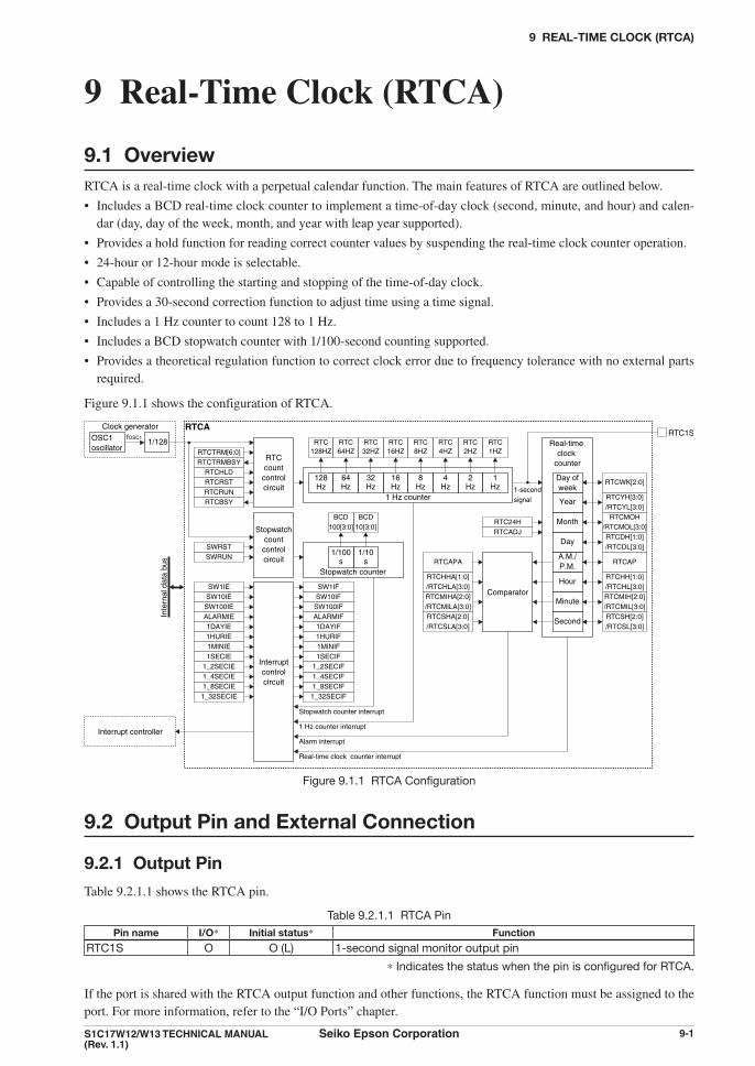
9 REAL-TIME CLOCK (RTCA)
S1C17W12/W13 TECHNICAL MANUAL Seiko Epson Corporation 9-1(Rev. 1.1)
9 Real-Time Clock (RTCA)
9.1 OverviewRTCA is a real-time clock with a perpetual calendar function. The main features of RTCA are outlined below.
• Includes a BCD real-time clock counter to implement a time-of-day clock (second, minute, and hour) and calen-dar (day, day of the week, month, and year with leap year supported).
• Provides a hold function for reading correct counter values by suspending the real-time clock counter operation.
• 24-hour or 12-hour mode is selectable.
• Capable of controlling the starting and stopping of the time-of-day clock.
• Provides a 30-second correction function to adjust time using a time signal.
• Includes a 1 Hz counter to count 128 to 1 Hz.
• Includes a BCD stopwatch counter with 1/100-second counting supported.
• Provides a theoretical regulation function to correct clock error due to frequency tolerance with no external parts required.
Figure 9.1.1 shows the configuration of RTCA.
RTCAfOSC1
1-secondsignal
RTCcount
control circuit
Comparator
OSC1oscillator
1/128
128Hz
RTCTRM[6:0]RTC
128HZ
64Hz
RTC64HZ
32Hz
RTC32HZ
16Hz
RTC16HZ
8Hz
RTC8HZ
4Hz
RTC4HZ
2Hz
RTC2HZ
1Hz
RTC1HZ
Clock generator
Interrupt controller
RTCTRMBSYRTCHLD
RTC24HRTCADJStopwatch
count control circuit
Interruptcontrolcircuit
SWRSTSWRUN
SW1IESW10IESW100IEALARMIE1DAYIE1HURIE1MINIE1SECIE
1_2SECIE1_4SECIE1_8SECIE1_32SECIE
SW1IFSW10IF
SW100IFALARMIF1DAYIF1HURIF1MINIF1SECIF
1_2SECIF1_4SECIF1_8SECIF1_32SECIF
RTCRSTRTCRUN
RTCWK[2:0]
RTCYH[3:0]/RTCYL[3:0]
RTCMOH/RTCMOL[3:0]RTCDH[1:0]/RTCDL[3:0]
RTCAP
RTCHH[1:0]/RTCHL[3:0]RTCMIH[2:0]/RTCMIL[3:0]RTCSH[2:0]/RTCSL[3:0]
RTCAPA
RTCHHA[1:0]/RTCHLA[3:0]RTCMIHA[2:0]/RTCMILA[3:0]RTCSHA[2:0]/RTCSLA[3:0]
RTCBSY
Day of week
Year
Month
Day
A.M./P.M.
Hour
Minute
Second
1 Hz counter
1/100 s
BCD100[3:0]
1/10s
BCD10[3:0]
Stopwatch counter
Stopwatch counter interrupt
1 Hz counter interrupt
Alarm interrupt
Real-time clock counter interrupt
Real-time clock
counter
RTC1S
Inte
rnal
dat
a bu
s
Figure 9.1.1 RTCA Configuration
9.2 Output Pin and External Connection
9.2.1 Output PinTable 9.2.1.1 shows the RTCA pin.
Table 9.2.1.1 RTCA PinPin name I/O* Initial status* Function
RTC1S O O (L) 1-second signal monitor output pin* Indicates the status when the pin is configured for RTCA.
If the port is shared with the RTCA output function and other functions, the RTCA function must be assigned to the port. For more information, refer to the “I/O Ports” chapter.

9 REAL-TIME CLOCK (RTCA)
9-2 Seiko Epson Corporation S1C17W12/W13 TECHNICAL MANUAL (Rev. 1.1)
9.3 Clock Settings
9.3.1 RTCA Operating ClockRTCA uses CLK_RTCA, which is generated by the clock generator from OSC1 as the clock source, as its operat-ing clock. RTCA is operable when OSC1 is enabled.To continue the RTCA operation during SLEEP mode with OSC1 being activated, the CLGOSC.OSC1SLPC bit must be set to 0.
9.3.2 Theoretical Regulation FunctionThe time-of-day clock loses accuracy if the OSC1 frequency fOSC1 has a frequency tolerance from 32.768 kHz. To correct this error without changing any external part, RTCA provides a theoretical regulation function. Follow the procedure below to perform theoretical regulation.
1. Measure the frequency tolerance “m [ppm]” of fOSC1.
2. Determine the theoretical regulation execution cycle time “n seconds.”
3. Determine the value to be written to the RTCCTL.RTCTRM[6:0] bits from the results in Steps 1 and 2.
4. Write the value determined in Step 3 to the RTCCTL.RTCTRM[6:0] bits periodically in n-second cycles using an RTCA alarm or second interrupt.
5. Monitor the RTC1S signal to check that every n-second cycle has no error included.
The correction value for theoretical regulation can be specified within the range from -64 to +63 and it should be written to the RTCCTL.RTCTRM[6:0] bits as a two’s-complement number. Use Eq. 9.1 to calculate the correction value.
mRTCTRM[6:0] = —— × 256 × n (However, RTCTRM[6:0] is an integer after rounding off to -64 to +63.) (Eq. 9.1) 106
Wheren: Theoretical regulation execution cycle time [second] (time interval to write the correct value to the RTCCTL.
RTCTRM[6:0] bits periodically via software)m: OSC1 frequency tolerance [ppm]
Figure 9.3.2.1 shows the RTC1S signal waveform.
RTC1S
RTCCTL.RTCTRMBSY
32,768/fOSC1 [s]
Theoretical regulation execution cycle time n [s]
32,768/fOSC1 ± ∆T [s]
∗ ∆T = correction time set in the RTCCTL.RTCTRM[6:0] bits
Writing to the RTCCTL.RTCTRM[6:0] bits Theoretical regulation completion interrupt
Figure 9.3.2.1 RTC1S Signal Waveform
Table 9.3.2.1 lists the frequency tolerance correction rates when the theoretical regulation execution cycle time n is 4,096 seconds as an example.
Table 9.3.2.1 Correction Rates when Theoretical Regulation Execution Cycle Time n = 4,096 SecondsRTCCTL.RTCTRM[6:0]
bits (two’s-complement)Correction
value (decimal)Correction rate
[ppm]RTCCTL.RTCTRM[6:0]
bits (two’s-complement)Correction
value (decimal)Correction rate
[ppm]0x00 0 0.0 0x40 -64 -61.00x01 1 1.0 0x41 -63 -60.10x02 2 1.9 0x42 -62 -59.10x03 3 2.9 0x43 -61 -58.2· · · · · · · · · · · · · · · · · ·
0x3e 62 59.1 0x7e -2 -1.90x3f 63 60.1 0x7f -1 -1.0
Minimum resolution: 1 ppm, Correction rate range: -61.0 to 60.1 ppm

9 REAL-TIME CLOCK (RTCA)
S1C17W12/W13 TECHNICAL MANUAL Seiko Epson Corporation 9-3(Rev. 1.1)
Notes: • The theoretical regulation affects only the real-time clock counter and 1 Hz counter. It does not affect the stopwatch counter.
• After a value is written to the RTCCTL.RTCTRM[6:0] bits, the theoretical regulation correction takes effect on the 1 Hz counter value at the same timing as when the 1 Hz counter changes to 0x7f. Also an interrupt occurs depending on the counter value at this time.
9.4 Operations
9.4.1 RTCA Control Follow the sequences shown below to set time to RTCA, to read the current time and to set alarm.
Time setting 1. Set RTCA to 12H or 24H mode using the RTCCTL.RTC24H bit.
2. Write 1 to the RTCCTL.RTCRUN bit to enable for the real-time clock counter to start counting up.
3. Check to see if the RTCCTL.RTCBSY bit = 0 that indicates the counter is ready to rewrite. If the RTCCTL.RTCBSY bit = 1, wait until it is set to 0.
4. Write the current date and time in BCD code to the control bits listed below. RTCSEC.RTCSH[2:0]/RTCSL[3:0] bits (second) RTCHUR.RTCMIH[2:0]/RTCMIL[3:0] bits (minute) RTCHUR.RTCHH[1:0]/RTCHL[3:0] bits (hour) RTCHUR.RTCAP bit (AM/PM) (effective when RTCCTL.RTC24H bit = 0) RTCMON.RTCDH[1:0]/RTCDL[3:0] bits (day) RTCMON.RTCMOH/RTCMOL[3:0] bits (month) RTCYAR.RTCYH[3:0]/RTCYL[3:0] bits (year) RTCYAR.RTCWK[2:0] bits (day of the week)
5 Write 1 to the RTCCTL.RTCADJ bit (execute 30-second correction) using a time signal to adjust the time. (For more information on the 30-second correction, refer to “Real-Time Clock Counter Operations.”)
6. Write 1 to the real-time clock counter interrupt flags in the RTCINTF register to clear them.
7. Write 1 to the interrupt enable bits in the RTCINTE register to enable real-time clock counter interrupts.
Time read1. Check to see if the RTCCTL.RTCBSY bit = 0. If the RTCCTL.RTCBSY bit = 1, wait until it is set to 0.
2. Write 1 to the RTCCTL.RTCHLD bit to suspend count-up operation of the real-time clock counter.
3. Read the date and time from the control bits listed in “Time setting, Step 4” above.
4. Write 0 to the RTCCTL.RTCHLD bit to resume count-up operation of the real-time clock counter. If a second count-up timing has occurred in the count hold state, the hardware corrects the second counter for +1 second (for more information on the +1 second correction, refer to “Real-Time Clock Counter Opera-tions”).
Alarm setting1. Write 0 to the RTCINTE.ALARMIE bit to 0 to disable alarm interrupts.
2. Write the alarm time in BCD code to the control bits listed below (a time within 24 hours from the current time can be specified). RTCALM1.RTCSHA[2:0]/RTCSLA[3:0] bits (second) RTCALM2.RTCMIHA[2:0]/RTCMILA[3:0] bits (minute) RTCALM2.RTCHHA[1:0]/RTCHLA[3:0] bits (hour) RTCALM2.RTCAPA bit (AM/PM) (effective when RTCCTL.RTC24H bit = 0)
3. Write 1 to the RTCINTF.ALARMIF bit to clear the alarm interrupt flag.
4. Write 1 to the RTCINTE.ALARMIE bit to enable alarm interrupts. When the real-time clock counter reaches the alarm time set in Step 2, an alarm interrupt occurs.

9 REAL-TIME CLOCK (RTCA)
9-4 Seiko Epson Corporation S1C17W12/W13 TECHNICAL MANUAL (Rev. 1.1)
9.4.2 Real-Time Clock Counter OperationsThe real-time clock counter consists of second, minute, hour, AM/PM, day, month, year, and day of the week coun-ters and it performs counting up using the RTC1S signal. It has the following functions as well.
Recognizing leap years The leap year recognizing algorithm used in RTCA is effective only for Christian Era years. Years within 0 to
99 that can be divided by four without a remainder are recognized as leap years. If the year counter = 0x00, RTCA assumes it as a common year. If a leap year is recognized, the count range of the day counter changes when the month counter is set to February.
Corrective operation when a value out of the effective range is set When a value out of the effective range is set to the year, day of the week, or hour (in 24H mode) counter, the
counter will be cleared to 0 at the next count-up timing. When a such value is set to the month, day, or hour (in 12H mode) counter, the counter will be set to 1 at the next count-up timing.
30-second correction This function is provided to set the time-of-day clock by the time signal. Writing 1 to the RTCCTL.RTCADJ
bit adds 1 to the minute counter if the second counter represents 30 to 59 seconds, or clears the second counter with the minute counter left unchanged if the second counter represents 0 to 29 seconds.
+1 second correction If a second count-up timing occurred while the RTCCTL.RTCHLD bit = 1 (count hold state), the real-time
clock counter counts up by +1 second (performs +1 second correction) after the counting has resumed by writ-ing 0 to the RTCCTL.RTCHLD bit.
Note: If two or more second count-up timings occurred while the RTCCTL.RTCHLD bit = 1, the coun-ter is always corrected for +1 second only.
9.4.3 Stopwatch ControlFollow the sequences shown below to start counting of the stopwatch and to read the counter.
Count start1. Write 1 to the RTCSWCTL.SWRST bit to reset the stopwatch counter.
2. Write 1 to the stopwatch interrupt flags in the RTCINTF register to clear them.
3. Write 1 to the interrupt enable bits in the RTCINTE register to enable stopwatch interrupts.
4. Write 1 to the RTCSWCTL.SWRUN bit to start stopwatch count up operation.
Counter read1. Read the count value from the RTCSWCTL.BCD10[3:0] and BCD100[3:0] bits.
2. Read again.i. If the two read values are the same, assume that the count values are read correctly. ii. If different values are read, perform reading once more and compare the read value with the previous one.
9.4.4 Stopwatch Count-up PatternThe stopwatch consists of 1/100-second and 1/10-second counters and these counters perform counting up in incre-ments of approximate 1/100 and 1/10 seconds with the count-up patterns shown in Figure 9.4.4.1.
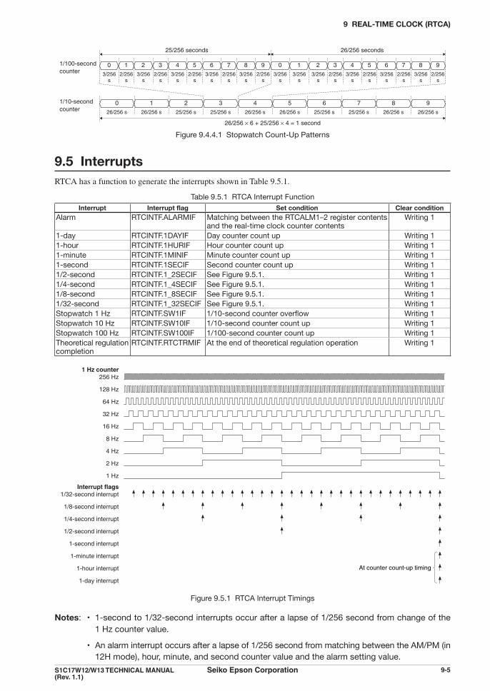
9 REAL-TIME CLOCK (RTCA)
S1C17W12/W13 TECHNICAL MANUAL Seiko Epson Corporation 9-5(Rev. 1.1)
26/256 × 6 + 25/256 × 4 = 1 second
1/100-secondcounter
26/256 seconds25/256 seconds
3/256s
0
1/10-secondcounter 26/256 s
0
26/256 s
1
25/256 s
2
25/256 s
3
26/256 s
4
26/256 s
5
25/256 s
6
25/256 s
7
26/256 s
8
26/256 s
9
3/256s
0
3/256s
1
2/256s
1
3/256s
2
2/256s
3
3/256s
4
2/256s
5
3/256s
6
2/256s
7
3/256s
8
2/256s
9
3/256s
2
2/256s
3
3/256s
4
2/256s
5
3/256s
6
2/256s
7
3/256s
8
2/256s
9
Figure 9.4.4.1 Stopwatch Count-Up Patterns
9.5 InterruptsRTCA has a function to generate the interrupts shown in Table 9.5.1.
Table 9.5.1 RTCA Interrupt FunctionInterrupt Interrupt flag Set condition Clear condition
Alarm RTCINTF.ALARMIF Matching between the RTCALM1–2 register contents and the real-time clock counter contents
Writing 1
1-day RTCINTF.1DAYIF Day counter count up Writing 11-hour RTCINTF.1HURIF Hour counter count up Writing 11-minute RTCINTF.1MINIF Minute counter count up Writing 11-second RTCINTF.1SECIF Second counter count up Writing 11/2-second RTCINTF.1_2SECIF See Figure 9.5.1. Writing 11/4-second RTCINTF.1_4SECIF See Figure 9.5.1. Writing 11/8-second RTCINTF.1_8SECIF See Figure 9.5.1. Writing 11/32-second RTCINTF.1_32SECIF See Figure 9.5.1. Writing 1Stopwatch 1 Hz RTCINTF.SW1IF 1/10-second counter overflow Writing 1Stopwatch 10 Hz RTCINTF.SW10IF 1/10-second counter count up Writing 1Stopwatch 100 Hz RTCINTF.SW100IF 1/100-second counter count up Writing 1Theoretical regulation completion
RTCINTF.RTCTRMIF At the end of theoretical regulation operation Writing 1
1 Hz counter256 Hz
128 Hz
64 Hz
32 Hz
16 Hz
8 Hz
4 Hz
2 Hz
1 Hz
Interrupt flags1/32-second interrupt
1/8-second interrupt
1/4-second interrupt
1/2-second interrupt
1-second interrupt
1-minute interrupt
1-hour interrupt
1-day interrupt
At counter count-up timing
Figure 9.5.1 RTCA Interrupt Timings
Notes: • 1-second to 1/32-second interrupts occur after a lapse of 1/256 second from change of the 1 Hz counter value.
• An alarm interrupt occurs after a lapse of 1/256 second from matching between the AM/PM (in 12H mode), hour, minute, and second counter value and the alarm setting value.

9 REAL-TIME CLOCK (RTCA)
9-6 Seiko Epson Corporation S1C17W12/W13 TECHNICAL MANUAL (Rev. 1.1)
RTCA provides interrupt enable bits corresponding to each interrupt flag. An interrupt request is sent to the inter-rupt controller only when the interrupt flag, of which interrupt has been enabled by the interrupt enable bit, is set. For more information on interrupt control, refer to the “Interrupt Controller” chapter.
9.6 Control Registers
RTC Control RegisterRegister name Bit Bit name Initial Reset R/W Remarks
RTCCTL 15 RTCTRMBSY 0 H0 R –14–8 RTCTRM[6:0] 0x00 H0 W Read as 0x00.
7 – 0 – R –6 RTCBSY 0 H0 R5 RTCHLD 0 H0 R/W Cleared by setting the
RTCCTL.RTCRST bit to 1.4 RTC24H 0 H0 R/W –3 – 0 – R2 RTCADJ 0 H0 R/W Cleared by setting the
RTCCTL.RTCRST bit to 1.1 RTCRST 0 H0 R/W –0 RTCRUN 0 H0 R/W
Bit 15 RTCTRMBSY This bit indicates whether the theoretical regulation is currently executed or not. 1 (R): Theoretical regulation is executing. 0 (R): Theoretical regulation has finished (or not executed).
This bit goes 1 when a value is written to the RTCCTL.RTCTRM[6:0] bits. The theoretical regulation takes up to 1 second for execution. This bit reverts to 0 automatically after the theoretical regulation has finished execution.
Bits 14–8 RTCTRM[6:0] Write the correction value for adjusting the 1 Hz frequency to these bits to execute theoretical regula-
tion. For a calculation method of correction value, refer to “Theoretical Regulation Function.”
Notes: • When the RTCCTL.RTCTRMBSY bit = 1, the RTCCTL.RTCTRM[6:0] bits cannot be rewritten.
• Writing 0x00 to the RTCCTL.RTCTRM[6:0] bits sets the RTCCTL.RTCTRMBSY bit to 1 as well. However, no correcting operation is performed.
Bit 7 Reserved
Bit 6 RTCBSY This bit indicates whether the counter is performing count-up operation or not. 1 (R): In count-up operation 0 (R): Idle (ready to rewrite real-time clock counter)
This bit goes 1 when performing 1-second count-up, +1 second correction, or 30-second correction. It retains 1 for 1/256 second and then reverts to 0.
Bit 5 RTCHLD This bit halts the count-up operation of the real-time clock counter. 1 (R/W): Halt real-time clock counter count-up operation 0 (R/W): Normal operation
Writing 1 to this bit halts the count-up operation of the real-time clock counter, this makes it possible to read the counter value correctly without changing the counter. Write 0 to this bit to resume count-up operation immediately after the counter has been read. Depending on these operation timings, the +1 second correction may be executed after the count-up operation resumes. For more information on the +1 second correction, refer to “Real-Time Clock Counter Operations.”

9 REAL-TIME CLOCK (RTCA)
S1C17W12/W13 TECHNICAL MANUAL Seiko Epson Corporation 9-7(Rev. 1.1)
Note: When the RTCCTL.RTCTRMBSY bit = 1, the RTCCTL.RTCHLD bit cannot be rewritten to 1 (as fixed at 0).
Bit 4 RTC24H This bit sets the hour counter to 24H mode or 12H mode. 1 (R/W): 24H mode 0 (R/W): 12H mode
This selection changes the count range of the hour counter. Note, however, that the counter value is not updated automatically, therefore, it must be programmed again.
Note: Be sure to avoid writing to this bit when the RTCCTL.RTCRUN bit = 1.
Bit 3 Reserved
Bit 2 RTCADJ This bit executes the 30-second correction time adjustment function. 1 (W): Execute 30-second correction 0 (W): Ineffective 1 (R): 30-second correction is executing. 0 (R): 30-second correction has finished. (Normal operation)
Writing 1 to this bit executes 30-second correction and an enabled interrupt occurs even if the RT-CCTL.RTCRUN bit = 0. The correction takes up to 2/256 seconds. The RTCCTL.RTCADJ bit is automatically cleared to 0 when the correction has finished. For more information on the 30-second correction, refer to “Real-Time Clock Counter Operations.”
Notes: • Be sure to avoid writing to this bit when the RTCCTL.RTCBSY bit = 1.
• Do not write 1 to this bit again while the RTCCTL.RTCADJ bit = 1.
Bit 1 RTCRST This bit resets the 1 Hz counter, the RTCCTL.RTCADJ bit, and the RTCCTL.RTCHLD bit. 1 (W): Reset 0 (W): Ineffective 1 (R): Reset is being executed. 0 (R): Reset has finished. (Normal operation)
This bit is automatically cleared to 0 after reset has finished.
Bit 0 RTCRUN This bit starts/stops the real-time clock counter. 1 (R/W): Running/start control 0 (R/W): Idle/stop control
When the real-time clock counter stops counting by writing 0 to this bit, the counter retains the value when it stopped. Writing 1 to this bit again resumes counting from the value retained.
RTC Second Alarm RegisterRegister name Bit Bit name Initial Reset R/W Remarks
RTCALM1 15 – 0 – R –14–12 RTCSHA[2:0] 0x0 H0 R/W11–8 RTCSLA[3:0] 0x0 H0 R/W7–0 – 0x00 – R
Bit 15 Reserved
Bits 14–12 RTCSHA[2:0]Bits 11–8 RTCSLA[3:0] The RTCALM1.RTCSHA[2:0] bits and the RTCALM1.RTCSLA[3:0] bits set the 10-second digit and
1-second digit of the alarm time, respectively. A value within 0 to 59 seconds can be set in BCD code as shown in Table 9.6.1.

9 REAL-TIME CLOCK (RTCA)
9-8 Seiko Epson Corporation S1C17W12/W13 TECHNICAL MANUAL (Rev. 1.1)
Table 9.6.1 Setting Examples in BCD CodeSetting value in BCD code Alarm (second) settingRTCALM1.RTCSHA[2:0] bits RTCALM1.RTCSLA[3:0] bits
0x0 0x0 00 seconds0x0 0x1 01 second· · · · · · · · ·0x0 0x9 09 seconds0x1 0x0 10 seconds· · · · · · · · ·0x5 0x9 59 seconds
Bits 7–0 Reserved
RTC Hour/Minute Alarm RegisterRegister name Bit Bit name Initial Reset R/W Remarks
RTCALM2 15 – 0 – R –14 RTCAPA 0 H0 R/W
13–12 RTCHHA[1:0] 0x0 H0 R/W11–8 RTCHLA[3:0] 0x0 H0 R/W
7 – 0 – R6–4 RTCMIHA[2:0] 0x0 H0 R/W3–0 RTCMILA[3:0] 0x0 H0 R/W
Bit 15 Reserved
Bit 14 RTCAPA This bit sets A.M. or P.M. of the alarm time in 12H mode (RTCCTL.RTC24H bit = 0). 1 (R/W): P.M. 0 (R/W): A.M.
This setting is ineffective in 24H mode (RTCCTL.RTC24H bit = 1).
Bits 13–12 RTCHHA[1:0]Bits 11–8 RTCHLA[3:0] The RTCALM2.RTCHHA[1:0] bits and the RTCALM2.RTCHLA[3:0] bits set the 10-hour digit and
1-hour digit of the alarm time, respectively. A value within 1 to 12 o’clock in 12H mode or 0 to 23 in 24H mode can be set in BCD code.
Bit 7 Reserved
Bits 6–4 RTCMIHA[2:0]Bits 3–0 RTCMILA[3:0] The RTCALM2.RTCMIHA[2:0] bits and the RTCALM2.RTCMILA[3:0] bits set the 10-minute digit
and 1-minute digit of the alarm time, respectively. A value within 0 to 59 minutes can be set in BCD code.
RTC Stopwatch Control RegisterRegister name Bit Bit name Initial Reset R/W Remarks
RTCSWCTL 15–12 BCD10[3:0] 0x0 H0 R –11–8 BCD100[3:0] 0x0 H0 R7–5 – 0x0 – R4 SWRST 0 H0 W Read as 0.
3–1 – 0x0 – R –0 SWRUN 0 H0 R/W
Bits 15–12 BCD10[3:0]Bits 11–8 BCD100[3:0] The 1/10-second and 1/100-second digits of the stopwatch counter can be read as a BCD code from
the RTCSWCTL.BCD10[3:0] bits and the RTCSWCTL.BCD100[3:0] bits, respectively.

9 REAL-TIME CLOCK (RTCA)
S1C17W12/W13 TECHNICAL MANUAL Seiko Epson Corporation 9-9(Rev. 1.1)
Note: The counter value may not be read correctly while the stopwatch counter is running. The RTCSWCTL.BCD10[3:0]/BCD100[3:0] bits must be read twice and assume the counter value was read successfully if the two read results are the same.
Bits 7–5 Reserved
Bit 4 SWRST This bit resets the stopwatch counter to 0x00. 1 (W): Reset 0 (W): Ineffective 0 (R): Always 0 when being read
When the stopwatch counter in running status is reset, it continues counting from count 0x00. The stopwatch counter retains 0x00 if it is reset in idle status.
Bits 3–1 Reserved
Bit 0 SWRUN This bit starts/stops the stopwatch counter. 1 (R/W): Running/start control 0 (R/W): Idle/stop control
When the stopwatch counter stops counting by writing 0 to this bit, the counter retains the value when it stopped. Writing 1 to this bit again resumes counting from the value retained.
Note: The stopwatch counter stops in sync with the stopwatch clock after 0 is written to the RTCSWCTL.SWRUN bit. Therefore, the counter value may be incremented (+1) from the value at writing 0.
RTC Second/1Hz RegisterRegister name Bit Bit name Initial Reset R/W Remarks
RTCSEC 15 – 0 – R –14–12 RTCSH[2:0] 0x0 H0 R/W11–8 RTCSL[3:0] 0x0 H0 R/W
7 RTC1HZ 0 H0 R Cleared by setting theRTCCTL.RTCRST bit to 1.6 RTC2HZ 0 H0 R
5 RTC4HZ 0 H0 R4 RTC8HZ 0 H0 R3 RTC16HZ 0 H0 R2 RTC32HZ 0 H0 R1 RTC64HZ 0 H0 R0 RTC128HZ 0 H0 R
Bit 15 Reserved
Bits 14–12 RTCSH[2:0]Bits 11–8 RTCSL[3:0] The RTCSEC.RTCSH[2:0] bits and the RTCSEC.RTCSL[3:0] bits are used to set and read the 10-sec-
ond digit and the 1-second digit of the second counter, respectively. The setting/read values are a BCD code within the range from 0 to 59.
Note: Be sure to avoid writing to the RTCSEC.RTCSH[2:0]/RTCSL[3:0] bits while the RTCCTL.RTCBSY bit = 1.

9 REAL-TIME CLOCK (RTCA)
9-10 Seiko Epson Corporation S1C17W12/W13 TECHNICAL MANUAL (Rev. 1.1)
Bit 7 RTC1HZBit 6 RTC2HZBit 5 RTC4HZBit 4 RTC8HZBit 3 RTC16HZBit 2 RTC32HZBit 1 RTC64HZBit 0 RTC128HZ 1 Hz counter data can be read from these bits. The following shows the correspondence between the bit and frequency: RTCSEC.RTC1HZ bit: 1 Hz RTCSEC.RTC2HZ bit: 2 Hz RTCSEC.RTC4HZ bit: 4 Hz RTCSEC.RTC8HZ bit: 8 Hz RTCSEC.RTC16HZ bit: 16 Hz RTCSEC.RTC32HZ bit: 32 Hz RTCSEC.RTC64HZ bit: 64 Hz RTCSEC.RTC128HZ bit: 128 Hz
Note: The counter value may not be read correctly while the 1 Hz counter is running. These bits must be read twice and assume the counter value was read successfully if the two read results are the same.
RTC Hour/Minute RegisterRegister name Bit Bit name Initial Reset R/W Remarks
RTCHUR 15 – 0 – R –14 RTCAP 0 H0 R/W
13–12 RTCHH[1:0] 0x1 H0 R/W11–8 RTCHL[3:0] 0x2 H0 R/W
7 – 0 – R6–4 RTCMIH[2:0] 0x0 H0 R/W3–0 RTCMIL[3:0] 0x0 H0 R/W
Bit 15 Reserved
Bit 14 RTCAP This bit is used to set and read A.M. or P.M. data in 12H mode (RTCCTL.RTC24H bit = 0). 1 (R/W): P.M. 0 (R/W): A.M.
In 24H mode (RTCCTL.RTC24H bit = 1), this bit is fixed at 0 and writing 1 is ignored. However, if the RTCHUR.RTCAP bit = 1 when changed to 24H mode, it goes 0 at the next count-up timing of the hour counter.
Bits 13–12 RTCHH[1:0]Bits 11–8 RTCHL[3:0] The RTCHUR.RTCHH[1:0] bits and the RTCHUR.RTCHL[3:0] bits are used to set and read the 10-
hour digit and the 1-hour digit of the hour counter, respectively. The setting/read values are a BCD code within the range from 1 to 12 in 12H mode or 0 to 23 in 24H mode.
Note: Be sure to avoid writing to the RTCHUR.RTCHH[1:0]/RTCHL[3:0] bits while the RTCCTL.RTCBSY bit = 1.
Bit 7 Reserved

9 REAL-TIME CLOCK (RTCA)
S1C17W12/W13 TECHNICAL MANUAL Seiko Epson Corporation 9-11(Rev. 1.1)
Bits 6–4 RTCMIH[2:0]Bits 3–0 RTCMIL[3:0] The RTCHUR.RTCMIH[2:0] bits and the RTCHUR.RTCMIL[3:0] bits are used to set and read the
10-minute digit and the 1-minute digit of the minute counter, respectively. The setting/read values are a BCD code within the range from 0 to 59.
Note: Be sure to avoid writing to the RTCHUR.RTCMIH[2:0]/RTCMIL[3:0] bits while the RTCCTL.RTCBSY bit = 1.
RTC Month/Day RegisterRegister name Bit Bit name Initial Reset R/W Remarks
RTCMON 15–13 – 0x0 – R –12 RTCMOH 0 H0 R/W
11–8 RTCMOL[3:0] 0x1 H0 R/W7–6 – 0x0 – R5–4 RTCDH[1:0] 0x0 H0 R/W3–0 RTCDL[3:0] 0x1 H0 R/W
Bits 15–13 Reserved
Bit 12 RTCMOHBits 11–8 RTCMOL[3:0] The RTCMON.RTCMOH bit and the RTCMON.RTCMOL[3:0] bits are used to set and read the
10-month digit and the 1-month digit of the month counter, respectively. The setting/read values are a BCD code within the range from 1 to 12.
Note: Be sure to avoid writing to the RTCMON.RTCMOH/RTCMOL[3:0] bits while the RTCCTL.RTCBSY bit = 1.
Bits 7–6 Reserved
Bits 5–4 RTCDH[1:0]Bits 3–0 RTCDL[3:0] The RTCMON.RTCDH[1:0] bits and the RTCMON.RTCDL[3:0] bits are used to set and read the 10-
day digit and the 1-day digit of the day counter, respectively. The setting/read values are a BCD code within the range from 1 to 31 (to 28 for February in a common year, to 29 for February in a leap year, or to 30 for April/June/September/November).
Note: Be sure to avoid writing to the RTCMON.RTCDH[1:0]/RTCDL[3:0] bits while the RTCCTL.RTCBSY bit = 1.
RTC Year/Week RegisterRegister name Bit Bit name Initial Reset R/W Remarks
RTCYAR 15–11 – 0x00 – R –10–8 RTCWK[2:0] 0x0 H0 R/W7–4 RTCYH[3:0] 0x0 H0 R/W3–0 RTCYL[3:0] 0x0 H0 R/W
Bits 15–11 Reserved
Bits 10–8 RTCWK[2:0] These bits are used to set and read day of the week. The day of the week counter is a base-7 counter and the setting/read values are 0x0 to 0x6. Table 9.6.2
lists the correspondence between the count value and day of the week.

9 REAL-TIME CLOCK (RTCA)
9-12 Seiko Epson Corporation S1C17W12/W13 TECHNICAL MANUAL (Rev. 1.1)
Table 9.6.2 Correspondence between the count value and day of the weekRTCYAR.RTCWK[2:0] bits Day of the week
0x6 Saturday0x5 Friday0x4 Thursday0x3 Wednesday0x2 Tuesday0x1 Monday0x0 Sunday
Note: Be sure to avoid writing to the RTCYAR.RTCWK[2:0] bits while the RTCCTL.RTCBSY bit = 1.
Bits 7–4 RTCYH[3:0]Bits 3–0 RTCYL[3:0] The RTCYAR.RTCYH[3:0] bits and the RTCYAR.RTCYL[3:0] bits are used to set and read the 10-
year digit and the 1-year digit of the year counter, respectively. The setting/read values are a BCD code within the range from 0 to 99.
Note: Be sure to avoid writing to the RTCYAR.RTCYH[3:0]/RTCYL[3:0] bits while the RTCCTL.RTCBSY bit = 1.
RTC Interrupt Flag RegisterRegister name Bit Bit name Initial Reset R/W Remarks
RTCINTF 15 RTCTRMIF 0 H0 R/W Cleared by writing 1.14 SW1IF 0 H0 R/W13 SW10IF 0 H0 R/W12 SW100IF 0 H0 R/W
11–9 – 0x0 – R –8 ALARMIF 0 H0 R/W Cleared by writing 1.7 1DAYIF 0 H0 R/W6 1HURIF 0 H0 R/W5 1MINIF 0 H0 R/W4 1SECIF 0 H0 R/W3 1_2SECIF 0 H0 R/W2 1_4SECIF 0 H0 R/W1 1_8SECIF 0 H0 R/W0 1_32SECIF 0 H0 R/W
Bit 15 RTCTRMIFBit 14 SW1IFBit 13 SW10IFBit 12 SW100IF These bits indicate the real-time clock interrupt cause occurrence status. 1 (R): Cause of interrupt occurred 0 (R): No cause of interrupt occurred 1 (W): Clear flag 0 (W): Ineffective
The following shows the correspondence between the bit and interrupt: RTCINTF.RTCTRMIF bit: Theoretical regulation completion interrupt RTCINTF.SW1IF bit: Stopwatch 1 Hz interrupt RTCINTF.SW10IF bit: Stopwatch 10 Hz interrupt RTCINTF.SW100IF bit: Stopwatch 100 Hz interrupt
Bits 11–9 Reserved

9 REAL-TIME CLOCK (RTCA)
S1C17W12/W13 TECHNICAL MANUAL Seiko Epson Corporation 9-13(Rev. 1.1)
Bit 8 ALARMIFBit 7 1DAYIFBit 6 1HURIFBit 5 1MINIFBit 4 1SECIFBit 3 1_2SECIFBit 2 1_4SECIFBit 1 1_8SECIFBit 0 1_32SECIF These bits indicate the real-time clock interrupt cause occurrence status. 1 (R): Cause of interrupt occurred 0 (R): No cause of interrupt occurred 1 (W): Clear flag 0 (W): Ineffective
The following shows the correspondence between the bit and interrupt: RTCINTF. ALARMIF bit: Alarm interrupt RTCINTF.1DAYIF bit: 1-day interrupt RTCINTF.1HURIF bit: 1-hour interrupt RTCINTF.1MINIF bit: 1-minute interrupt RTCINTF.1SECIF bit: 1-second interrupt RTCINTF.1_2SECIF bit: 1/2-second interrupt RTCINTF.1_4SECIF bit: 1/4-second interrupt RTCINTF.1_8SECIF bit: 1/8-second interrupt RTCINTF.1_32SECIF bit: 1/32-second interrupt
RTC Interrupt Enable RegisterRegister name Bit Bit name Initial Reset R/W Remarks
RTCINTE 15 RTCTRMIE 0 H0 R/W –14 SW1IE 0 H0 R/W13 SW10IE 0 H0 R/W12 SW100IE 0 H0 R/W
11–9 – 0x0 – R8 ALARMIE 0 H0 R/W7 1DAYIE 0 H0 R/W6 1HURIE 0 H0 R/W5 1MINIE 0 H0 R/W4 1SECIE 0 H0 R/W3 1_2SECIE 0 H0 R/W2 1_4SECIE 0 H0 R/W1 1_8SECIE 0 H0 R/W0 1_32SECIE 0 H0 R/W
Bit 15 RTCTRMIEBit 14 SW1IEBit 13 SW10IEBit 12 SW100IE These bits enable real-time clock interrupts. 1 (R/W): Enable interrupts 0 (R/W): Disable interrupts
The following shows the correspondence between the bit and interrupt: RTCINTE.RTCTRMIE bit: Theoretical regulation completion interrupt RTCINTE.SW1IE bit: Stopwatch 1 Hz interrupt RTCINTE.SW10IE bit: Stopwatch 10 Hz interrupt RTCINTE.SW100IE bit: Stopwatch 100 Hz interrupt

9 REAL-TIME CLOCK (RTCA)
9-14 Seiko Epson Corporation S1C17W12/W13 TECHNICAL MANUAL (Rev. 1.1)
Bits 11–9 Reserved
Bit 8 ALARMIEBit 7 1DAYIEBit 6 1HURIEBit 5 1MINIEBit 4 1SECIEBit 3 1_2SECIEBit 2 1_4SECIEBit 1 1_8SECIEBit 0 1_32SECIE These bits enable real-time clock interrupts. 1 (R/W): Enable interrupts 0 (R/W): Disable interrupts
The following shows the correspondence between the bit and interrupt: RTCINTE.ALARMIE bit: Alarm interrupt RTCINTE.1DAYIE bit: 1-day interrupt RTCINTE.1HURIE bit: 1-hour interrupt RTCINTE.1MINIE bit: 1-minute interrupt RTCINTE.1SECIE bit: 1-second interrupt RTCINTE.1_2SECIE bit: 1/2-second interrupt RTCINTE.1_4SECIE bit: 1/4-second interrupt RTCINTE.1_8SECIE bit: 1/8-second interrupt RTCINTE.1_32SECIE bit: 1/32-second interrupt

10 SUPPLY VOLTAGE DETECTOR (SVD)
S1C17W12/W13 TECHNICAL MANUAL Seiko Epson Corporation 10-1(Rev. 1.1)
10 Supply Voltage Detector (SVD)
10.1 OverviewSVD is a supply voltage detector to monitor the power supply voltage on the VDD pin or the voltage applied to an external pin. The main features are listed below.
• Power supply voltage to be detected: Selectable from VDD and an external power supply (EXSVD)
• Detectable voltage level: Selectable from among 30 levels (1.2 to 3.6 V)
• Detection results: - Can be read whether the power supply voltage is lower than the detection voltage level or not.
- Can generate an interrupt or a reset when low power supply voltage is de-tected.
• Interrupt: 1 system (Low power supply voltage detection interrupt)
• Supports intermittent operations: - Three detection cycles are selectable.
- Low power supply voltage detection count function to generate an inter-rupt/reset when low power supply voltage is successively detected the number of times specified.
- Continuous operation is also possible.
Figure 10.1.1 shows the configuration of SVD.
SVD
To system reset circuit
To interrupt controller
SVDMD[1:0]
Sampling timinggenerator
Voltagecomparator
circuit
Interrupt/reset control circuit
Detection result counter
MODEN
SVDC[4:0]
VDSEL
SVDSC[1:0]
SVDIE
SVDIF
SVDDT
SVDRE[3:0]
CLKSRC[1:0]CLKDIV[2:0]Clock generator
CLK_SVD
VDD
EXSVD
DBRUN
Inte
rnal
dat
a bu
s
Figure 10.1.1 SVD Configuration

10 SUPPLY VOLTAGE DETECTOR (SVD)
10-2 Seiko Epson Corporation S1C17W12/W13 TECHNICAL MANUAL (Rev. 1.1)
10.2 Input Pin and External Connection
10.2.1 Input PinTable 10.2.1.1 shows the SVD input pin.
Table 10.2.1.1 SVD Input PinPin name I/O* Initial status* Function
EXSVD A A (Hi-Z) External power supply voltage detection pin (Not available in the TQFP12-48pin package)* Indicates the status when the pin is configured for SVD.
If the port is shared with the EXSVD pin and other functions, the EXSVD function must be assigned to the port be-fore SVD can be activated. For more information, refer to the “I/O Ports” chapter.
10.2.2 External Connection
SVDExternal power supply/regulator
etc.SVD
analog blockEXSVD
REXTREXSVD
VSS
Figure 10.2.2.1 Connection between EXSVD Pin and External Power Supply
REXT resistance value must be determined so that it will be sufficiently smaller than the EXSVD input impedance REXSVD. For the EXSVD pin input voltage range and the EXSVD input impedance, refer to “Supply Voltage Detec-tor Characteristics” in the “Electrical Characteristics” chapter.
10.3 Clock Settings
10.3.1 SVD Operating ClockWhen using SVD, the SVD operating clock CLK_SVD must be supplied to SVD from the clock generator.The CLK_SVD supply should be controlled as in the procedure shown below.
1. Write 0x0096 to the MSCPROT.PROT[15:0] bits. (Remove system protection)
2. Enable the clock source in the clock generator if it is stopped (refer to “Clock Generator” in the “Power Supply, Reset, and Clocks” chapter).
3. Set the following SVDCLK register bits:- SVDCLK.CLKSRC[1:0] bits (Clock source selection)- SVDCLK.CLKDIV[2:0] bits (Clock division ratio selection = Clock frequency setting)
4. Write a value other than 0x0096 to the MSCPROT.PROT[15:0] bits. (Set system protection)
The CLK_SVD frequency should be set to around 32 kHz.
10.3.2 Clock Supply in SLEEP ModeWhen using SVD during SLEEP mode, the SVD operating clock CLK_SVD must be configured so that it will keep supplying by writing 0 to the CLGOSC.xxxxSLPC bit for the CLK_SVD clock source.If the CLGOSC.xxxxSLPC bit for the CLK_SVD clock source is 1, the CLK_SVD clock source is deactivated dur-ing SLEEP mode and SVD stops with the register settings maintained at those before entering SLEEP mode. After the CPU returns to normal mode, CLK_SVD is supplied and the SVD operation resumes.

10 SUPPLY VOLTAGE DETECTOR (SVD)
S1C17W12/W13 TECHNICAL MANUAL Seiko Epson Corporation 10-3(Rev. 1.1)
10.3.3 Clock Supply in DEBUG ModeThe CLK_SVD supply during DEBUG mode should be controlled using the SVDCLK.DBRUN bit.The CLK_SVD supply to SVD is suspended when the CPU enters DEBUG mode if the SVDCLK.DBRUN bit = 0. After the CPU returns to normal mode, the CLK_SVD supply resumes. Although SVD stops operating when the CLK_SVD supply is suspended, the registers retain the status before DEBUG mode was entered. If the SVDCLK.DBRUN bit = 1, the CLK_SVD supply is not suspended and SVD will keep operating in DEBUG mode.
10.4 Operations
10.4.1 SVD ControlStarting detection SVD should be initialized and activated with the procedure listed below.
1. Write 0x0096 to the MSCPROT.PROT[15:0] bits. (Remove system protection)
2. Configure the operating clock using the SVDCLK.CLKSRC[1:0] and SVDCLK.CLKDIV[2:0] bits.
3. Set the following SVDCTL register bits:- SVDCTL.VDSEL bit (Select detection voltage (VDD or EXSVD))- SVDCTL.SVDSC[1:0] bits (Set low power supply voltage detection counter)- SVDCTL.SVDC[4:0] bits (Set SVD detection voltage VSVD)- SVDCTL.SVDRE[3:0] bits (Select reset/interrupt mode)- SVDCTL.SVDMD[1:0] bits (Set intermittent operation mode)
4. Set the following bits when using the interrupt:- Write 1 to the SVDINTF.SVDIF bit. (Clear interrupt flag)- Set the SVDINTE.SVDIE bit to 1. (Enable SVD interrupt)
5. Set the SVDCTL.MODEN bit to 1. (Enable SVD detection)
6. Write a value other than 0x0096 to the MSCPROT.PROT[15:0] bits. (Set system protection)
Terminating detection Follow the procedure shown below to stop SVD operation.
1. Write 0x0096 to the MSCPROT.PROT[15:0] bits. (Remove system protection)
2. Write 0 to the SVDCTL.MODEN bit. (Disable SVD detection)
3. Write a value other than 0x0096 to the MSCPROT.PROT[15:0] bits. (Set system protection)
Reading detection results The following two detection results can be obtained by reading the SVDINTF.SVDDT bit:
• Power supply voltage (VDD or EXSVD) ≥ SVD detection voltage VSVD when SVDINTF.SVDDT bit = 0
• Power supply voltage (VDD or EXSVD) < SVD detection voltage VSVD when SVDINTF.SVDDT bit = 1
Before reading the SVDINTF.SVDDT bit, wait for at least SVD circuit enable response time after 1 is written to the SVDCTL.MODEN bit (refer to “Supply Voltage Detector Characteristics, SVD circuit enable response time tSVDEN” in the “Electrical Characteristics” chapter).
After the SVDCTL.SVDC[4:0] bits setting value is altered to change the SVD detection voltage VSVD when the SVDCTL.MODEN bit = 1, wait for at least SVD circuit response time before reading the SVDINTF.SVDDT bit (refer to “Supply Voltage Detector Characteristics, SVD circuit response time tSVD” in the “Electrical Char-acteristics” chapter).

10 SUPPLY VOLTAGE DETECTOR (SVD)
10-4 Seiko Epson Corporation S1C17W12/W13 TECHNICAL MANUAL (Rev. 1.1)
10.4.2 SVD OperationsContinuous operation mode SVD operates in continuous operation mode by default (SVDCTL.SVDMD[1:0] bits = 0x0). In this mode,
SVD operates continuously while the SVDCTL.MODEN bit is set to 1 and it keeps loading the detection re-sults to the SVDINTF.SVDDT bit. During this period, the current detection results can be obtained by reading the SVDINTF.SVDDT bit as necessary. Furthermore, an interrupt (if the SVDCTL.SVDRE[3:0] bits ≠ 0xa) or a reset (if the SVDCTL.SVDRE[3:0] bits = 0xa) can be generated when the SVDINTF.SVDDT bit is set to 1 (low power supply voltage is detected). This mode can keep detecting power supply voltage drop after the voltage detection masking time has elapsed even if the IC is placed into SLEEP status or accidental clock stoppage has occurred.
Intermittent operation mode SVD operates in intermittent operation mode when the SVDCTL.SVDMD[1:0] bits are set to 0x1 to 0x3. In
this mode, SVD turns on at an interval set using the SVDCTL.SVDMD[1:0] bits to perform detection operation and then it turns off while the SVDCTL.MODEN bit is set to 1. During this period, the latest detection results can be obtained by reading the SVDINTF.SVDDT bit as necessary. Furthermore, an interrupt or a reset can be generated when SVD has successively detected low power supply voltage the number of times specified by the SVDCTL.SVDSC[1:0] bits.
(1) When the SVDCTL.SVDMD[1:0] bits = 0x0 (continuous operation mode)VSVDVSVDVDD
SVDCTL.MODEN
SVD operating status
SVDINTF.SVDDTLow power supply voltage
detection interrupt
DET
(2) When the SVDCTL.SVDMD[1:0] bits ≠ 0x0 (intermittent operation mode)
VSVD : Level set using the SVDCTL.SVDC[4:0] bits : Voltage detection masking time : Voltage detection operation
DET
VSVDVSVDVDD
SVDCTL.MODEN
SVD operating status
SVDINTF.SVDDTLow power supply voltage
detection interrupt
DET
DET
Figure 10.4.2.1 SVD Operations
10.5 SVD Interrupt and Reset
10.5.1 SVD InterruptSetting the SVDCTL.SVDRE[3:0] bits to a value other than 0xa allows use of the low power supply voltage detec-tion interrupt function.
Table 10.5.1.1 Low Power Supply Voltage Detection Interrupt FunctionInterrupt Interrupt flag Set condition Clear condition
Low power supply voltage detection
SVDINTF.SVDIF In continuous operation modeWhen the SVDINTF.SVDDT bit is 1
In intermittent operation modeWhen low power supply voltage is successively de-tected the specified number of times
Writing 1
SVD provides the interrupt enable bit (SVDINTE.SVDIE bit) corresponding to the interrupt flag (SVDINTF.SVDIF bit). An interrupt request is sent to the interrupt controller only when the SVDINTF.SVDIF bit is set while the interrupt is enabled by the SVDINTE.SVDIE bit. For more information on interrupt control, refer to the “Interrupt Controller” chapter.

10 SUPPLY VOLTAGE DETECTOR (SVD)
S1C17W12/W13 TECHNICAL MANUAL Seiko Epson Corporation 10-5(Rev. 1.1)
Once the SVDINTF.SVDIF bit is set, it will not be cleared even if the power supply voltage subsequently returns to a value exceeding the SVD detection voltage VSVD. An interrupt may occur due to a temporary power supply voltage drop, check the power supply voltage status by reading the SVDINTF.SVDDT bit in the interrupt handler routine.
10.5.2 SVD ResetSetting the SVDCTL.SVDRE[3:0] bits to 0xa allows use of the SVD reset issuance function.The reset issuing timing is the same as that of the SVDINTF.SVDIF bit being set when a low voltage is detected.After a reset has been issued, SVD enters continuous operation mode even if it was operating in intermittent opera-tion mode, and continues operating. Issuing an SVD reset initializes the port assignment. However, when EXSVD is being detected, the input of the port for the EXSVD pin is sent to SVD so that SVD will continue the EXSVD detection operation. If the power supply voltage reverts to the normal level, the SVDINTF.SVDDT bit goes 0 and the reset state is can-celed. After that, SVD resumes operating in the operation mode set previously via the initialization routine.During reset state, the SVD control bits are set as shown in Table 10.5.2.1.
Table 10.5.2.1 SVD Control Bits During Reset StateControl register Control bit SettingSVDCLK DBRUN Reset to the initial values.
CLKDIV[2:0]CLKSRC[1:0]
SVDCTL VDSEL The set value is retained.SVDSC[1:0] Cleared to 0. (The set value becomes invalid as SVD en-
ters continuous operation mode.)SVDC[4:0] The set value is retained.SVDRE[3:0] The set value (0xa) is retained.SVDMD[1:0] Cleared to 0 to set continuous operation mode.MODEN The set value (1) is retained.
SVDINTF SVDIF The status (1) before being reset is retained.SVDINTE SVDIE Cleared to 0.
10.6 Control Registers
SVD Clock Control RegisterRegister name Bit Bit name Initial Reset R/W Remarks
SVDCLK 15–9 – 0x00 – R –8 DBRUN 1 H0 R/WP7 – 0 – R
6–4 CLKDIV[2:0] 0x0 H0 R/WP3–2 – 0x0 – R1–0 CLKSRC[1:0] 0x0 H0 R/WP
Bits 15–9 Reserved
Bit 8 DBRUN This bit sets whether the SVD operating clock is supplied in DEBUG mode or not. 1 (R/WP): Clock supplied in DEBUG mode 0 (R/WP): No clock supplied in DEBUG mode
Bit 7 Reserved
Bits 6–4 CLKDIV[2:0] These bits select the division ratio of the SVD operating clock.
Bits 3–2 Reserved
Bits 1–0 CLKSRC[1:0] These bits select the clock source of SVD.

10 SUPPLY VOLTAGE DETECTOR (SVD)
10-6 Seiko Epson Corporation S1C17W12/W13 TECHNICAL MANUAL (Rev. 1.1)
Table 10.6.1 Clock Source and Division Ratio Settings
SVDCLK.CLKDIV[2:0] bits
SVDCLK.CLKSRC[1:0] bits0x0 0x1 0x2 0x3
IOSC OSC1 OSC3 EXOSC0x6, 0x7 Reserved 1/1 Reserved 1/1
0x5 1/128 1/1280x4 1/64 1/640x3 1/32 1/320x2 1/16 1/160x1 1/8 1/80x0 1/4 1/4
(Note) The oscillation circuits/external input that are not supported in this IC cannot be selected as the clock source.
Note: The clock frequency should be set to around 32 kHz.
SVD Control RegisterRegister name Bit Bit name Initial Reset R/W Remarks
SVDCTL 15 VDSEL 0 H1 R/WP –14–13 SVDSC[1:0] 0x0 H0 R/WP Writing takes effect when the SVDCTL.
SVDMD[1:0] bits are not 0x0.12–8 SVDC[4:0] 0x1e H1 R/WP –7–4 SVDRE[3:0] 0x0 H1 R/WP3 – 0 – R
2–1 SVDMD[1:0] 0x0 H0 R/WP0 MODEN 0 H1 R/WP
Bit 15 VDSEL This bit selects the power supply voltage to be detected by SVD. 1 (R/WP): Voltage applied to the EXSVD pin 0 (R/WP): VDD
Bits 14–13 SVDSC[1:0] These bits set the condition to generate an interrupt/reset (number of successive low voltage detec-
tions) in intermittent operation mode (SVDCTL.SVDMD[1:0] bits = 0x1 to 0x3).
Table 10.6.2 Interrupt/Reset Generating Condition in Intermittent Operation ModeSVDCTL.SVDSC[1:0] bits Interrupt/reset generating condition
0x3 Low power supply voltage is successively detected eight times.0x2 Low power supply voltage is successively detected four times.0x1 Low power supply voltage is successively detected twice.0x0 Low power supply voltage is successively detected once.
This setting is ineffective in continuous operation mode (SVDCTL.SVDMD[1:0] bits = 0x0).
Bits 12–8 SVDC[4:0] These bits select an SVD detection voltage VSVD for detecting low voltage from among 30 levels.
Table 10.6.3 Setting of SVD Detection Voltage VSVD
SVDCTL.SVDC[4:0] bits SVD detection voltage VSVD [V]0x1e High0x1d ↑0x1c
:0x02 ↓0x01 Low
0x00, 0x1f Use prohibited
For more information, refer to “Supply Voltage Detector Characteristics, SVD detection voltage VSVD” in the “Electrical Characteristics” chapter.

10 SUPPLY VOLTAGE DETECTOR (SVD)
S1C17W12/W13 TECHNICAL MANUAL Seiko Epson Corporation 10-7(Rev. 1.1)
Bits 7–4 SVDRE[3:0] These bits enable/disable the reset issuance function when a low power supply voltage is detected. 0xa (R/WP): Enable (Issue reset) Other than 0xa (R/WP): Disable (Generate interrupt)
For more information on the SVD reset issuance function, refer to “SVD Reset.”
Bit 3 Reserved
Bits 2–1 SVDMD[1:0] These bits select intermittent operation mode and its detection cycle.
Table 10.6.4 Intermittent Operation Mode Detection Cycle SelectionSVDCTL.SVDMD[1:0] bits Operation mode (detection cycle)
0x3 Intermittent operation mode (CLK_SVD/512)0x2 Intermittent operation mode (CLK_SVD/256)0x1 Intermittent operation mode (CLK_SVD/128)0x0 Continuous operation mode
For more information on intermittent and continuous operation modes, refer to “SVD Operations.”
Bit 0 MODEN This bit enables/disables for the SVD circuit to operate. 1 (R/WP): Enable (Start detection operations) 0 (R/WP): Disable (Stop detection operations)
After this bit has been altered, wait until the value written is read out from this bit without subsequent operations being performed.
Notes: • Writing 0 to the SVDCTL.MODEN bit resets the SVD hardware. However, the register values set and the interrupt flag are not cleared. The SVDCTL.MODEN bit is actually set to 0 after this processing has finished. If 1 is written to the SVDCTL.MODEN bit continuously without waiting for the bit being read as 0 at this time, writing 0 may be ignored and a malfunction may occur as the hardware restarts without resetting.
• The SVD internal circuit is initialized if the SVDCTL.SVDSC[1:0] bits, SVDCTL.SVDRE[3:0] bits, or SVDCTL.SVDMD[1:0] bits are altered while SVD is in operation after 1 is written to the SVDCTL.MODEN bit.
SVD Status and Interrupt Flag RegisterRegister name Bit Bit name Initial Reset R/W Remarks
SVDINTF 15–9 – 0x00 – R –8 SVDDT x – R
7–1 – 0x00 – R0 SVDIF 0 H1 R/W Cleared by writing 1.
Bits 15–9 Reserved
Bit 8 SVDDT The power supply voltage detection results can be read out from this bit. 1 (R): Power supply voltage (VDD or EXSVD) < SVD detection voltage VSVD
0 (R): Power supply voltage (VDD or EXSVD) ≥ SVD detection voltage VSVD
Bits 7–1 Reserved
Bit 0 SVDIF This bit indicates the low power supply voltage detection interrupt cause occurrence status. 1 (R): Cause of interrupt occurred 0 (R): No cause of interrupt occurred 1 (W): Clear flag 0 (W): Ineffective

10 SUPPLY VOLTAGE DETECTOR (SVD)
10-8 Seiko Epson Corporation S1C17W12/W13 TECHNICAL MANUAL (Rev. 1.1)
Note: The SVD internal circuit is initialized if the interrupt flag is cleared while SVD is in operation after 1 is written to the SVDCTL.MODEN bit.
SVD Interrupt Enable RegisterRegister name Bit Bit name Initial Reset R/W Remarks
SVDINTE 15–8 – 0x00 – R –7–1 – 0x00 – R0 SVDIE 0 H0 R/W
Bits 15–1 Reserved
Bit 0 SVDIE This bit enables low power supply voltage detection interrupts. 1 (R/W): Enable interrupts 0 (R/W): Disable interrupts
Notes: • If the SVDCTL.SVDRE[3:0] bits are set to 0xa, no low power supply voltage detection interrupt will occur, as a reset is issued at the same timing as an interrupt.
• To prevent generating unnecessary interrupts, the corresponding interrupt flag should be cleared before enabling interrupts.

11 16-BIT TIMERS (T16)
S1C17W12/W13 TECHNICAL MANUAL Seiko Epson Corporation 11-1(Rev. 1.1)
11 16-bit Timers (T16)
11.1 OverviewT16 is a 16-bit timer. The features of T16 are listed below.
• 16-bit presettable down counter
• Provides a reload data register for setting the preset value.
• A clock source and clock division ratio for generating the count clock are selectable.
• Repeat mode or one-shot mode is selectable.
• Can generate counter underflow interrupts.
Figure 11.1.1 shows the configuration of a T16 channel.
Table 11.1.1 T16 Channel Configuration of S1C17W12/W13Item S1C17W12 S1C17W13
Number of channels 3 channels (Ch.0–Ch.2)Event counter function Not supported (No EXCLm pins are provided.)Peripheral clock output(Outputs the counter underflow signal.)
Ch.1 → Synchronous serial interface Ch.0 master clock
T16 Ch.n
To interrupt controller
(To peripheral circuit)
Underflow
PRESETTimer control
circuit
Interrupt control circuit
PRUN
TRMD
CLKSRC[1:0]CLKDIV[3:0]Clock generator
UFIE
UFIF
DBRUNMODEN
CLK_T16_nTimer counter
TC[15:0]
Reload registerTR[15:0]
Inte
rnal
dat
a bu
s
EXCLm( )
Figure 11.1.1 Configuration of a T16 Channel
11.2 Input PinTable 11.2.1 shows the T16 input pin.
Table 11.2.1 T16 Input PinPin name I/O* Initial status* Function
EXCLm I I (Hi-Z) External event signal input pin* Indicates the status when the pin is configured for T16.
If the port is shared with the EXCLm pin and other functions, the EXCLm input function must be assigned to the port before using the event counter function. For more information, refer to the “I/O Ports” chapter.

11 16-BIT TIMERS (T16)
11-2 Seiko Epson Corporation S1C17W12/W13 TECHNICAL MANUAL (Rev. 1.1)
11.3 Clock Settings
11.3.1 T16 Operating ClockWhen using T16 Ch.n, the T16 Ch.n operating clock CLK_T16_n must be supplied to T16 Ch.n from the clock generator. The CLK_T16_n supply should be controlled as in the procedure shown below.
1. Enable the clock source in the clock generator if it is stopped (refer to “Clock Generator” in the “Power Supply, Reset, and Clocks” chapter).
2. Set the following T16_nCLK register bits:- T16_nCLK.CLKSRC[1:0] bits (Clock source selection)- T16_nCLK.CLKDIV[3:0] bits (Clock division ratio selection = Clock frequency setting)
11.3.2 Clock Supply in SLEEP ModeWhen using T16 during SLEEP mode, the T16 operating clock CLK_T16_n must be configured so that it will keep supplying by writing 0 to the CLGOSC.xxxxSLPC bit for the CLK_T16_n clock source.If the CLGOSC.xxxxSLPC bit for the CLK_T16_n clock source is 1, the CLK_T16_n clock source is deactivated during SLEEP mode and T16 stops with the register settings and counter value maintained at those before entering SLEEP mode. After the CPU returns to normal mode, CLK_T16_n is supplied and the T16 operation resumes.
11.3.3 Clock Supply in DEBUG ModeThe CLK_T16_n supply during DEBUG mode should be controlled using the T16_nCLK.DBRUN bit.The CLK_T16_n supply to T16 Ch.n is suspended when the CPU enters DEBUG mode if the T16_nCLK.DBRUN bit = 0. After the CPU returns to normal mode, the CLK_T16_n supply resumes. Although T16 Ch.n stops operat-ing when the CLK_T16_n supply is suspended, the counter and registers retain the status before DEBUG mode was entered. If the T16_nCLK.DBRUN bit = 1, the CLK_T16_n supply is not suspended and T16 Ch.n will keep operating in DEBUG mode.
11.3.4 Event Counter ClockThe channel that supports the event counter function counts down at the rising edge of the EXCLm pin input signal when the T16_nCLK.CLKSRC[1:0] bits are set to 0x3.
EXCLm pin input
Counter x x - 1 x - 2 x - 3
Figure 11.3.4.1 Count Down Timing
Note that the EXOSC clock is selected for the channel that does not support the event counter function.
11.4 Operations
11.4.1 InitializationT16 Ch.n should be initialized and started counting with the procedure shown below.
1. Configure the T16 Ch.n operating clock (see “T16 Operating Clock”).
2. Set the T16_nCTL.MODEN bit to 1. (Enable count operation clock)
3. Set the T16_nMOD.TRMD bit. (Select operation mode (Repeat mode or One-shot mode)).
4. Set the T16_nTR register. (Set reload data (counter preset data))
5. Set the following bits when using the interrupt:- Write 1 to the T16_nINTF.UFIF bit. (Clear interrupt flag)- Set the T16_nINTE.UFIE bit to 1. (Enable underflow interrupt)

11 16-BIT TIMERS (T16)
S1C17W12/W13 TECHNICAL MANUAL Seiko Epson Corporation 11-3(Rev. 1.1)
6. Set the following T16_nCTL register bits:- Set the T16_nCTL.PRESET bit to 1. (Preset reload data to counter)- Set the T16_nCTL.PRUN bit to 1. (Start counting)
11.4.2 Counter UnderflowNormally, the T16 counter starts counting down from the reload data value preset and generates an underflow signal when an underflow occurs. This signal is used to generate an interrupt and may be output to a specific peripheral circuit as a clock (T16 Ch.n must be set to repeat mode to generate a clock). The underflow cycle is determined by the T16 Ch.n operating clock setting and reload data (counter initial value) set in the T16_nTR register. The following shows the equations to calculate the underflow cycle and frequency:
TR + 1 fCLK_T16_nT = ————— fT = ————— (Eq. 11.1) fCLK_T16_n TR + 1
WhereT: Underflow cycle [s]fT: Underflow frequency [Hz]TR: T16_nTR register settingfCLK_T16_n: T16 Ch.n operating clock frequency [Hz]
11.4.3 Operations in Repeat ModeT16 Ch.n enters repeat mode by setting the T16_nMOD.TRMD bit to 0.In repeat mode, the count operation starts by writing 1 to the T16_nCTL.PRUN bit and continues until 0 is written. A counter underflow presets the T16_nTR register value to the counter, so underflow occurs periodically. Select this mode to generate periodic underflow interrupts or when using the timer to output a trigger/clock to the periph-eral circuit.
Counter
0xffff
0x0000
Software control
Underflow interrupt
Underflow cycle
Time
T16_nTRregister setting
PRESET = 1PRUN = 1 PRUN = 1
PRUN = 0
Figure 11.4.3.1 Count Operations in Repeat Mode
11.4.4 Operations in One-shot ModeT16 Ch.n enters one-shot mode by setting the T16_nMOD.TRMD bit to 1.In one-shot mode, the count operation starts by writing 1 to the T16_nCTL.PRUN bit and stops after the T16_nTR register value is preset to the counter when an underflow has occurred. At the same time the counter stops, the T16_nCTL.PRUN bit is cleared automatically. Select this mode to stop the counter after an interrupt has occurred once, such as for checking a specific lapse of time.

11 16-BIT TIMERS (T16)
11-4 Seiko Epson Corporation S1C17W12/W13 TECHNICAL MANUAL (Rev. 1.1)
0xffff
0x0000
PRESET = 1PRUN = 1
PRUN = 1PRUN = 0
PRUN = 1 PRUN = 1
Counter
Software control
Underflow interrupt
Underflow cycle
Time
T16_nTRregister setting
Figure 11.4.4.1 Count Operations in One-shot Mode
11.4.5 Counter Value ReadThe counter value can be read out from the T16_nTC.TC[15:0] bits. However, since T16 operates on CLK_T16_n, one of the operations shown below is required to read correctly by the CPU.
- Read the counter value twice or more and check to see if the same value is read.
- Stop the timer and then read the counter value.
11.5 InterruptEach T16 channel has a function to generate the interrupt shown in Table 11.5.1.
Table 11.5.1 T16 Interrupt FunctionInterrupt Interrupt flag Set condition Clear condition
Underflow T16_nINTF.UFIF When the counter underflows Writing 1
T16 provides interrupt enable bits corresponding to each interrupt flag. An interrupt request is sent to the interrupt controller only when the interrupt flag, of which interrupt has been enabled by the interrupt enable bit, is set. For more information on interrupt control, refer to the “Interrupt Controller” chapter.
11.6 Control Registers
T16 Ch.n Clock Control RegisterRegister name Bit Bit name Initial Reset R/W Remarks
T16_nCLK 15–9 – 0x00 – R –8 DBRUN 0 H0 R/W
7–4 CLKDIV[3:0] 0x0 H0 R/W3–2 – 0x0 – R1–0 CLKSRC[1:0] 0x0 H0 R/W
Bits 15–9 Reserved
Bit 8 DBRUN This bit sets whether the T16 Ch.n operating clock is supplied in DEBUG mode or not. 1 (R/W): Clock supplied in DEBUG mode 0 (R/W): No clock supplied in DEBUG mode
Bits 7–4 CLKDIV[3:0] These bits select the division ratio of the T16 Ch.n operating clock (counter clock).
Bits 3–2 Reserved
Bits 1–0 CLKSRC[1:0] These bits select the clock source of T16 Ch.n.

11 16-BIT TIMERS (T16)
S1C17W12/W13 TECHNICAL MANUAL Seiko Epson Corporation 11-5(Rev. 1.1)
Table 11.6.1 Clock Source and Division Ratio Settings
T16_nCLK.CLKDIV[3:0] bits
T16_nCLK.CLKSRC[1:0] bits0x0 0x1 0x2 0x3
IOSC OSC1 OSC3 EXOSC/EXCLm0xf 1/32,768 1/1 1/32,768 1/10xe 1/16,384 1/16,3840xd 1/8,192 1/8,1920xc 1/4,096 1/4,0960xb 1/2,048 1/2,0480xa 1/1,024 1/1,0240x9 1/512 1/5120x8 1/256 1/256 1/2560x7 1/128 1/128 1/1280x6 1/64 1/64 1/640x5 1/32 1/32 1/320x4 1/16 1/16 1/160x3 1/8 1/8 1/80x2 1/4 1/4 1/40x1 1/2 1/2 1/20x0 1/1 1/1 1/1
(Note 1) The oscillation circuits/external input that are not supported in this IC cannot be selected as the clock source.
(Note 2) When the T16_nCLK.CLKSRC[1:0] bits are set to 0x3, EXCLm is selected for the channel with an event counter function or EXOSC is selected for other channels.
T16 Ch.n Mode RegisterRegister name Bit Bit name Initial Reset R/W Remarks
T16_nMOD 15–8 – 0x00 – R –7–1 – 0x00 – R0 TRMD 0 H0 R/W
Bits 15–1 Reserved
Bit 0 TRMD This bit selects the T16 operation mode. 1 (R/W): One-shot mode 0 (R/W): Repeat mode
For detailed information on the operation mode, refer to “Operations in One-shot Mode” and “Operations in Repeat Mode.”
T16 Ch.n Control RegisterRegister name Bit Bit name Initial Reset R/W Remarks
T16_nCTL 15–9 – 0x00 – R –8 PRUN 0 H0 R/W
7–2 – 0x00 – R1 PRESET 0 H0 R/W0 MODEN 0 H0 R/W
Bits 15–9 Reserved
Bit 8 PRUN This bit starts/stops the timer. 1 (W): Start timer 0 (W): Stop timer 1 (R): Timer is running 0 (R): Timer is idle

11 16-BIT TIMERS (T16)
11-6 Seiko Epson Corporation S1C17W12/W13 TECHNICAL MANUAL (Rev. 1.1)
By writing 1 to this bit, the timer starts count operations. However, the T16_nCTL.MODEN bit must be set to 1 in conjunction with this bit or it must be set in advance. While the timer is running, writing 0 to this bit stops count operations. When the counter stops due to a counter underflow in one-shot mode, this bit is automatically cleared to 0.
Bits 7–2 Reserved
Bit 1 PRESET This bit presets the reload data stored in the T16_nTR register to the counter. 1 (W): Preset 0 (W): Ineffective 1 (R): Presetting in progress 0 (R): Presetting finished or normal operation
By writing 1 to this bit, the timer presets the T16_nTR register value to the counter. However, the T16_nCTL.MODEN bit must be set to 1 in conjunction with this bit or it must be set in advance. This bit retains 1 during presetting and is automatically cleared to 0 after presetting has finished.
Bit 0 MODEN This bit enables the T16 Ch.n operations. 1 (R/W): Enable (Start supplying operating clock) 0 (R/W): Disable (Stop supplying operating clock)
T16 Ch.n Reload Data RegisterRegister name Bit Bit name Initial Reset R/W Remarks
T16_nTR 15–0 TR[15:0] 0xffff H0 R/W –
Bits 15–0 TR[15:0] These bits are used to set the initial value to be preset to the counter. The value set to this register will be preset to the counter when 1 is written to the T16_nCTL.PRESET
bit or when the counter underflows.
Notes: • The T16_nTR register cannot be altered while the timer is running (T16_nCTL.PRUN bit = 1), as an incorrect initial value may be preset to the counter.
• When one-shot mode is set, the T16_nTR.TR[15:0] bits should be set to a value equal to or greater than 0x0001.
T16 Ch.n Counter Data RegisterRegister name Bit Bit name Initial Reset R/W Remarks
T16_nTC 15–0 TC[15:0] 0xffff H0 R –
Bits 15–0 TC[15:0] The current counter value can be read out from these bits.
T16 Ch.n Interrupt Flag RegisterRegister name Bit Bit name Initial Reset R/W Remarks
T16_nINTF 15–8 – 0x00 – R –7–1 – 0x00 – R0 UFIF 0 H0 R/W Cleared by writing 1.
Bits 15–1 Reserved
Bit 0 UFIF This bit indicates the T16 Ch.n underflow interrupt cause occurrence status. 1 (R): Cause of interrupt occurred 0 (R): No cause of interrupt occurred 1 (W): Clear flag 0 (W): Ineffective

11 16-BIT TIMERS (T16)
S1C17W12/W13 TECHNICAL MANUAL Seiko Epson Corporation 11-7(Rev. 1.1)
T16 Ch.n Interrupt Enable RegisterRegister name Bit Bit name Initial Reset R/W Remarks
T16_nINTE 15–8 – 0x00 – R –7–1 – 0x00 – R0 UFIE 0 H0 R/W
Bits 15–1 Reserved
Bit 0 UFIE This bit enables T16 Ch.n underflow interrupts. 1 (R/W): Enable interrupts 0 (R/W): Disable interrupts
Note: To prevent generating unnecessary interrupts, the corresponding interrupt flag should be cleared before enabling interrupts.

12 UART (UART2)
S1C17W12/W13 TECHNICAL MANUAL Seiko Epson Corporation 12-1(Rev. 1.1)
12 UART (UART2)
12.1 OverviewThe UART2 is an asynchronous serial interface. The features of the UART2 are listed below.
• Includes a baud rate generator for generating the transfer clock.
• Supports 7- and 8-bit data length (LSB first).
• Odd parity, even parity, or non-parity mode is selectable.
• The start bit length is fixed at 1 bit.
• The stop bit length is selectable from 1 bit and 2 bits.
• Supports full-duplex communications.
• Includes a 2-byte receive data buffer and a 1-byte transmit data buffer.
• Includes an RZI modulator/demodulator circuit to support IrDA 1.0-compatible infrared communications.
• Can detect parity error, framing error, and overrun error.
• Can generate receive buffer full (1 byte/2 bytes), transmit buffer empty, end of transmission, parity error, framing error, and overrun error interrupts.
• Input pin can be pulled up with an internal resistor.
• The output pin is configurable as an open-drain output.
Figure 12.1.1 shows the UART2 configuration.
Table 12.1.1 UART2 Channel Configuration of S1C17W12/W13Item S1C17W12 S1C17W13
Number of channels 2 channels (Ch.0 and Ch.1)
UART2 Ch.n
Interrupt control circuit
Baud rate generator
Transmit/receive control circuit
Receive data buffer RXD[7:0]
Clock generator
Interruptcontroller
CLK_UART2_n
Shift register RZI demodulator
Transmit data buffer TXD[7:0]
Shift register RZI modulator
PUEN
OUTMD
IRMD
FMD[3:0]BRT[7:0]BRDIV
USINn
USOUTn
CLKSRC[1:0]CLKDIV[1:0]
DBRUNMODEN
TENDIEFEIEPEIEOEIE
RB2FIERB1FIETBEIE
TENDIFFEIFPEIFOEIF
RB2FIFRB1FIFTBEIF
STPB
SFTRST
RBSYTBSY
PRMDPRENCHLN
Inte
rnal
dat
a bu
s
INVTX
INVRX
Figure 12.1.1 UART2 Configuration

12 UART (UART2)
12-2 Seiko Epson Corporation S1C17W12/W13 TECHNICAL MANUAL (Rev. 1.1)
12.2 Input/Output Pins and External Connections
12.2.1 List of Input/Output PinsTable 12.2.1.1 lists the UART2 pins.
Table 12.2.1.1 List of UART2 PinsPin name I/O* Initial status* Function
USINn I I (Hi-Z) UART2 Ch.n data input pinUSOUTn O O (High) UART2 Ch.n data output pin
* Indicates the status when the pin is configured for the UART2.
If the port is shared with the UART2 pin and other functions, the UART2 input/output function must be assigned to the port before activating the UART2. For more information, refer to the “I/O Ports” chapter.
12.2.2 External ConnectionsFigure 12.2.2.1 shows a connection diagram between the UART2 in this IC and an external UART device.
USINn
USOUTn
OUT
IN
S1C17 UART2 External UART
Figure 12.2.2.1 Connections between UART2 and an External UART Device
12.2.3 Input Pin Pull-Up FunctionThe UART2 includes a pull-up resistor for the USINn pin. Setting the UAnMOD.PUEN bit to 1 enables the resistor to pull up the USINn pin.
12.2.4 Output Pin Open-Drain Output Function The USOUTn pin supports the open-drain output function. Default configuration is a push-pull output and it is switched to an open-drain output by setting the UAnMOD.OUTMD bit to 1.
12.2.5 Input/Output Signal Inverting FunctionThe UART2 can invert the signal polarities of the USINn pin input and the USOUTn pin output by setting the UAn-MOD.INVRX bit and the UAnMOD.INVTX bit, respectively, to 1.
Note: Unless otherwise specified, this chapter shows input/output signals with non-inverted wave-forms (UAnMOD.INVRX bit = 0, UAnMOD.INVTX bit =0).
12.3 Clock Settings
12.3.1 UART2 Operating ClockWhen using the UART2 Ch.n, the UART2 Ch.n operating clock CLK_UART2_n must be supplied to the UART2 Ch.n from the clock generator. The CLK_UART2_n supply should be controlled as in the procedure shown below.
1. Enable the clock source in the clock generator if it is stopped (refer to “Clock Generator” in the “Power Supply, Reset, and Clocks” chapter).
2. Set the following UAnCLK register bits:- UAnCLK.CLKSRC[1:0] bits (Clock source selection)- UAnCLK.CLKDIV[1:0] bits (Clock division ratio selection = Clock frequency setting)
The UART2 operating clock should be selected so that the baud rate generator will be configured easily.

12 UART (UART2)
S1C17W12/W13 TECHNICAL MANUAL Seiko Epson Corporation 12-3(Rev. 1.1)
12.3.2 Clock Supply in SLEEP ModeWhen using the UART2 during SLEEP mode, the UART2 operating clock CLK_UART2_n must be configured so that it will keep supplying by writing 0 to the CLGOSC.xxxxSLPC bit for the CLK_UART2_n clock source.
12.3.3 Clock Supply in DEBUG ModeThe CLK_UART2_n supply during DEBUG mode should be controlled using the UAnCLK.DBRUN bit.The CLK_UART2_n supply to the UART2 Ch.n is suspended when the CPU enters DEBUG mode if the UAnCLK.DBRUN bit = 0. After the CPU returns to normal mode, the CLK_UART2_n supply resumes. Although the UART2 Ch.n stops operating when the CLK_UART2_n supply is suspended, the output pin and registers retain the status before DEBUG mode was entered. If the UAnCLK.DBRUN bit = 1, the CLK_UART2_n supply is not suspended and the UART2 Ch.n will keep operating in DEBUG mode.
12.3.4 Baud Rate GeneratorThe UART2 includes a baud rate generator to generate the transfer (sampling) clock. The transfer rate is determined by the UAnMOD.BRDIV, UAnBR.BRT[7:0], and UAnBR.FMD[3:0] bit settings. Use the following equations to calculate the setting values for obtaining the desired transfer rate.
CLK_UART2 CLK_UART2bps = ————————— BRT = BRDIV × (—————— - FMD) - 1 (Eq. 12.1) BRT + 1 bps ———— + FMD BRDIVWhere
bps: Transfer rate [bit/s]CLK_UART2: UART2 operating clock frequency [Hz]BRDIV: Baud rate division ratio (1/16 or 1/4) *Selected by the UAnMOD.BRDIV bitBRT: UAnBR.BRT[7:0] setting value (0 to 255)FMD: UAnBR.FMD[3:0] setting value (0 to 15)
For the transfer rate range configurable in the UART2, refer to “UART Characteristics, Transfer baud rates UBRT1 and UBRT2” in the “Electrical Characteristics” chapter.
12.4 Data FormatThe UART2 allows setting of the data length, stop bit length, and parity function. The start bit length is fixed at one bit.
Data length With the UAnMOD.CHLN bit, the data length can be set to seven bits (UAnMOD.CHLN bit = 0) or eight bits
(UAnMOD.CHLN bit = 1).
Stop bit length With the UAnMOD.STPB bit, the stop bit length can be set to one bit (UAnMOD.STPB bit = 0) or two bits
(UAnMOD.STPB bit = 1).
Parity function The parity function is configured using the UAnMOD.PREN and UAnMOD.PRMD bits.
Table 12.4.1 Parity Function SettingUAnMOD.PREN bit UAnMOD.PRMD bit Parity function
1 1 Odd parity1 0 Even parity0 * Non parity

12 UART (UART2)
12-4 Seiko Epson Corporation S1C17W12/W13 TECHNICAL MANUAL (Rev. 1.1)
UAnMOD registerPREN bit
0
1
0
1
0
1
0
1
STPB bit0
0
1
1
0
0
1
1
CHLN bit0
0
0
0
1
1
1
1
st: start bit, sp: stop bit, p: parity bit
st D0 D1 D2 D3 D4 D5 D6 sp
st D0 D1 D2 D3 D4 D5 D6 p sp
st D0 D1 D2 D3 D4 D5 D6 sp sp
st D0 D1 D2 D3 D4 D5 D6 p sp sp
st D0 D1 D2 D3 D4 D5 D6 D7 sp
st D0 D1 D2 D3 D4 D5 D6 D7 p sp
st D0 D1 D2 D3 D4 D5 D6 D7 sp sp
st D0 D1 D2 D3 D4 D5 D6 D7 p sp sp
Figure 12.4.1 Data Format
12.5 Operations
12.5.1 InitializationThe UART2 Ch.n should be initialized with the procedure shown below.
1. Assign the UART2 Ch.n input/output function to the ports. (Refer to the “I/O Ports” chapter.)
2. Set the UAnCLK.CLKSRC[1:0] and UAnCLK.CLKDIV[1:0] bits. (Configure operating clock)
3. Configure the following UAnMOD register bits:- UAnMOD.BRDIV bit (Select baud rate division ratio (1/16 or 1/4))- UAnMOD.INVRX bit (Enable/disable USINn input signal inversion)- UAnMOD.INVTX bit (Enable/disable USOUTn output signal inversion)- UAnMOD.PUEN bit (Enable/disable USINn pin pull-up)- UAnMOD.OUTMD bit (Enable/disable USOUTn pin open-drain output)- UAnMOD.IRMD bit (Enable/disable IrDA interface)- UAnMOD.CHLN bit (Set data length (7 or 8 bits))- UAnMOD.PREN bit (Enable/disable parity function)- UAnMOD.PRMD bit (Select parity mode (even or odd))- UAnMOD.STPB bit (Set stop bit length (1 or 2 bits))
4. Set the UAnBR.BRT[7:0] and UAnBR.FMD[3:0] bits. (Set transfer rate)
5. Set the following UAnCTL register bits:- Set the UAnCTL.SFTRST bit to 1. (Execute software reset)- Set the UAnCTL.MODEN bit to 1. (Enable UART2 Ch.n operations)
6. Set the following bits when using the interrupt:- Write 1 to the interrupt flags in the UAnINTF register. (Clear interrupt flags)- Set the interrupt enable bits in the UAnINTE register to 1. * (Enable interrupts)
* The initial value of the UAnINTF.TBEIF bit is 1, therefore, an interrupt will occur immediately after the UA-nINTE.TBEIE bit is set to 1.

12 UART (UART2)
S1C17W12/W13 TECHNICAL MANUAL Seiko Epson Corporation 12-5(Rev. 1.1)
12.5.2 Data TransmissionA data sending procedure and the UART2 Ch.n operations are shown below. Figures 12.5.2.1 and 12.5.2.2 show a timing chart and a flowchart, respectively.
Data sending procedure1. Check to see if the UAnINTF.TBEIF bit is set to 1 (transmit buffer empty).
2. Write transmit data to the UAnTXD register.
3. Wait for a UART2 interrupt when using the interrupt.
4. Repeat Steps 1 to 3 (or 1 and 2) until the end of transmit data.
UART2 data sending operations The UART2 Ch.n starts data sending operations when transmit data is written to the UAnTXD register. The transmit data in the UAnTXD register is automatically transferred to the shift register and the UAnINTF.
TBEIF bit is set to 1 (transmit buffer empty). The USOUTn pin outputs a start bit and the UAnINTF.TBSY bit is set to 1 (transmit busy). The shift register
data bits are then output successively from the LSB. Following output of MSB, the parity bit (if parity is en-abled) and the stop bit are output.
Even if transmit data is being output from the USOUTn pin, the next transmit data can be written to the UAnTXD register after making sure the UAnINTF.TBEIF bit is set to 1.
If no transmit data remains in the UAnTXD register after the stop bit has been output from the USOUTn pin, the UAnINTF.TBSY bit is cleared to 0 and the UAnINTF.TENDIF bit is set to 1 (transmission completed).
USOUTn
UAnINTF.TBEIF
UAnINTF.TBSY
UAnINTF.TENDIF
Software operations
st D0 D1 D2 D3 D4 D5 D6 D7 p sp st D0 D1 D7 p sp st D0 D1 D7 p sp
(st: start bit, sp: stop bit, p: parity bit)
Data (W) → UAnTXD Data (W) → UAnTXD
1 (W) → UAnINTF.TENDIFData (W) → UAnTXD
Figure 12.5.2.1 Example of Data Sending Operations
Data transmission
End
Read the UAnINTF.TBEIF bit
Write transmit data to the UAnTXD register
YES
NO
NO
YESTransmit data remained?
UAnINTF.TBEIF = 1 ?
Wait for an interrupt request(UAnINTF.TBEIF = 1)
Figure 12.5.2.2 Data Transmission Flowchart

12 UART (UART2)
12-6 Seiko Epson Corporation S1C17W12/W13 TECHNICAL MANUAL (Rev. 1.1)
12.5.3 Data ReceptionA data receiving procedure and the UART2 Ch.n operations are shown below. Figures 12.5.3.1 and 12.5.3.2 show a timing chart and flowcharts, respectively.
Data receiving procedure (read by one byte)1. Wait for a UART2 interrupt when using the interrupt.
2. Check to see if the UAnINTF.RB1FIF bit is set to 1 (receive buffer one byte full).
3. Read the received data from the UAnRXD register.
4. Repeat Steps 1 to 3 (or 2 and 3) until the end of data reception.
Data receiving procedure (read by two bytes)1. Wait for a UART2 interrupt when using the interrupt.
2. Check to see if the UAnINTF.RB2FIF bit is set to 1 (receive buffer two bytes full).
3. Read the received data from the UAnRXD register twice.
4. Repeat Steps 1 to 3 (or 2 and 3) until the end of data reception.
UART2 data receiving operations The UART2 Ch.n starts data receiving operations when a start bit is input to the USINn pin. After the receive circuit has detected a low level as a start bit, it starts sampling the following data bits and
loads the received data into the receive shift register. The UAnINTF.RBSY bit is set to 1 when the start bit is detected.
The UAnINTF.RBSY bit is cleared to 0 and the receive shift register data is transferred to the receive data buf-fer at the stop bit receive timing.
The receive data buffer consists of a 2-byte FIFO and receives data until it becomes full. When the receive data buffer receives the first data, it sets the UAnINTF.RB1FIF bit to 1 (receive buffer one byte full). If the second data is received without reading the first data, the UAnINTF.RB2FIF bit is set to 1 (receive buffer two bytes full).
USINn
UAnINTF.RB1FIF
UAnINTF.RB2FIF
UAnINTF.RBSY
Software operations
st D0 ··· p sp st D0 ··· p sp st D0 ··· p sp st D0 ··· p sp
(st: start bit, sp: stop bit, p: parity bit)
data 1 data 2 data 3 data 4
UAnRXD → data 1 (R) UAnRXD → data 3 (R)
UAnRXD → data 2 (R)
Figure 12.5.3.1 Example of Data Receiving Operations
Data reception (1 byte read)
End
Wait for an interrupt request(UAnINTF.RB1FIF = 1)
Read receive data (1 byte) from the UAnRXD register
NO
YESReceive data remained?
Data reception (2 bytes read)
End
Wait for an interrupt request(UAnINTF.RB2FIF = 1)
Read receive data (1 byte) from the UAnRXD register
Read receive data (1 byte) from the UAnRXD register
NO
YESReceive data remained?
Figure 12.5.3.2 Data Reception Flowcharts

12 UART (UART2)
S1C17W12/W13 TECHNICAL MANUAL Seiko Epson Corporation 12-7(Rev. 1.1)
12.5.4 IrDA InterfaceThis UART2 includes an RZI modulator/demodulator circuit enabling implementation of IrDA 1.0-compatible in-frared communication function simply by adding simple external circuits.Set the UAnMOD.IRMD bit to 1 to use the IrDA interface.Data transfer control is identical to that for normal interface even if the IrDA interface function is enabled.
USINn
VDD
VSS
USOUTn
RXD
VCC
GND
TXD
LEDA
S1C17 UART2 Infrared communication module
AMP
GND
VCC
Figure 12.5.4.1 Example of Connections with an Infrared Communication Module
The transmit data output from the UART2 Ch.n transmit shift register is output from the USOUTn pin after the low pulse width is converted into 3/16 by the RZI modulator in SIR method.
Modulator input (shift register output)
Modulator output (USOUTn)
T1
T13
16T1
316
Figure 12.5.4.2 IrDA Transmission Signal Waveform
The received IrDA signal is input to the RZI demodulator and the low pulse width is converted into the normal width before input to the receive shift register.
Demodulator input (USINn)
Demodulator output (shift register input)
T2
Figure 12.5.4.3 IrDA Receive Signal Waveform
Notes: • Set the baud rate division ratio to 1/16 when using the IrDA interface function.
• The low pulse width (T2) of the IrDA signal input must be CLK_UART2 × 3 cycles or longer.
12.6 Receive ErrorsThree different receive errors, framing error, parity error, and overrun error, may be detected while receiving data. Since receive errors are interrupt causes, they can be processed by generating interrupts.
12.6.1 Framing ErrorThe UART2 determines loss of sync if a stop bit is not detected (when the stop bit is received as 0) and assumes that a framing error has occurred. The received data that encountered an error is still transferred to the receive data buffer and the UAnINTF.FEIF bit (framing error interrupt flag) is set to 1 when the data becomes ready to read from the UAnRXD register.

12 UART (UART2)
12-8 Seiko Epson Corporation S1C17W12/W13 TECHNICAL MANUAL (Rev. 1.1)
Note: Framing error/parity error interrupt flag set timings These interrupt flags will be set after the data that encountered an error is transferred to the re-
ceive data buffer. Note, however, that the set timing depends on the buffer status at that point.• When the receive data buffer is empty The interrupt flag will be set when the data that encountered an error is transferred to the re-
ceive data buffer.• When the receive data buffer has a one-byte free space The interrupt flag will be set when the first data byte already loaded is read out after the data
that encountered an error is transferred to the second byte entry of the receive data buffer.
12.6.2 Parity ErrorIf the parity function is enabled, a parity check is performed when data is received. The UART2 checks matching between the data received in the shift register and its parity bit, and issues a parity error if the result is a non-match. The received data that encountered an error is still transferred to the receive data buffer and the UAnINTF.PEIF bit (parity error interrupt flag) is set to 1 when the data becomes ready to read from the UAnRXD register (see the Note on framing error).
12.6.3 Overrun ErrorIf the receive data buffer is still full (two bytes of received data have not been read) when a data reception to the shift register has completed, an overrun error occurs as the data cannot be transferred to the receive data buffer.When an overrun error occurs, the UAnINTF.OEIF bit (overrun error interrupt flag) is set to 1.
12.7 InterruptsThe UART2 has a function to generate the interrupts shown in Table 12.7.1.
Table 12.7.1 UART2 Interrupt FunctionInterrupt Interrupt flag Set condition Clear condition
End of transmission UAnINTF.TENDIF When the UAnINTF.TBEIF bit = 1 after the stop bit has been sent
Writing 1 or software reset
Framing error UAnINTF.FEIF Refer to the “Receive Errors.” Writing 1, reading received data that encountered an error, or software reset
Parity error UAnINTF.PEIF Refer to the “Receive Errors.” Writing 1, reading received data that encountered an error, or software reset
Overrun error UAnINTF.OEIF Refer to the “Receive Errors.” Writing 1 or software resetReceive buffer two bytes full UAnINTF.RB2FIF When the second received data byte is
loaded to the receive data buffer in which the first byte is already received
Reading received data or software reset
Receive buffer one byte full UAnINTF.RB1FIF When the first received data byte is load-ed to the emptied receive data buffer
Reading data to empty the receive data buffer or software reset
Transmit buffer empty UAnINTF.TBEIF When transmit data written to the trans-mit data buffer is transferred to the shift register
Writing transmit data
The UART2 provides interrupt enable bits corresponding to each interrupt flag. An interrupt request is sent to the interrupt controller only when the interrupt flag, of which interrupt has been enabled by the interrupt enable bit, is set. For more information on interrupt control, refer to the “Interrupt Controller” chapter.

12 UART (UART2)
S1C17W12/W13 TECHNICAL MANUAL Seiko Epson Corporation 12-9(Rev. 1.1)
12.8 Control Registers
UART2 Ch.n Clock Control RegisterRegister name Bit Bit name Initial Reset R/W Remarks
UAnCLK 15–9 – 0x00 – R –8 DBRUN 0 H0 R/W
7–6 – 0x0 – R5–4 CLKDIV[1:0] 0x0 H0 R/W3–2 – 0x0 – R1–0 CLKSRC[1:0] 0x0 H0 R/W
Bits 15–9 Reserved
Bit 8 DBRUN This bit sets whether the UART2 operating clock is supplied in DEBUG mode or not. 1 (R/W): Clock supplied in DEBUG mode 0 (R/W): No clock supplied in DEBUG mode
Bits 7–6 Reserved
Bits 5–4 CLKDIV[1:0] These bits select the division ratio of the UART2 operating clock.
Bits 3–2 Reserved
Bits 1–0 CLKSRC[1:0] These bits select the clock source of the UART2.
Table 12.8.1 Clock Source and Division Ratio Settings
UAnCLK.CLKDIV[1:0] bits
UAnCLK.CLKSRC[1:0] bits0x0 0x1 0x2 0x3
IOSC OSC1 OSC3 EXOSC0x3 1/8 1/1 1/8 1/10x2 1/4 1/40x1 1/2 1/20x0 1/1 1/1
(Note) The oscillation circuits/external input that are not supported in this IC cannot be selected as the clock source.
Note: The UAnCLK register settings can be altered only when the UAnCTL.MODEN bit = 0.
UART2 Ch.n Mode RegisterRegister name Bit Bit name Initial Reset R/W Remarks
UAnMOD 15–11 – 0x00 – R –10 BRDIV 0 H0 R/W9 INVRX 0 H0 R/W8 INVTX 0 H0 R/W7 – 0 – R6 PUEN 0 H0 R/W5 OUTMD 0 H0 R/W4 IRMD 0 H0 R/W3 CHLN 0 H0 R/W2 PREN 0 H0 R/W1 PRMD 0 H0 R/W0 STPB 0 H0 R/W
Bits 15–11 Reserved

12 UART (UART2)
12-10 Seiko Epson Corporation S1C17W12/W13 TECHNICAL MANUAL (Rev. 1.1)
Bit 10 BRDIV This bit sets the UART2 operating clock division ratio for generating the transfer (sampling) clock
using the baud rate generator. 1 (R/W): 1/4 0 (R/W): 1/16
Bit 9 INVRX This bit enables the USINn input inverting function. 1 (R/W): Enable input inverting function 0 (R/W): Disable input inverting function
Bit 8 INVTX This bit enables the USOUTn output inverting function. 1 (R/W): Enable output inverting function 0 (R/W): Disable output inverting function
Bit 7 Reserved
Bit 6 PUEN This bit enables pull-up of the USINn pin. 1 (R/W): Enable pull-up 0 (R/W): Disable pull-up
Bit 5 OUTMD This bit sets the USOUTn pin output mode. 1 (R/W): Open-drain output 0 (R/W): Push-pull output
Bit 4 IRMD This bit enables the IrDA interface function. 1 (R/W): Enable IrDA interface function 0 (R/W): Disable IrDA interface function
Bit 3 CHLN This bit sets the data length. 1 (R/W): 8 bits 0 (R/W): 7 bits
Bit 2 PREN This bit enables the parity function. 1 (R/W): Enable parity function 0 (R/W): Disable parity function
Bit 1 PRMD This bit selects either odd parity or even parity when using the parity function. 1 (R/W): Odd parity 0 (R/W): Even parity
Bit 0 STPB This bit sets the stop bit length. 1 (R/W): 2 bits 0 (R/W): 1 bit
Note: The UAnMOD register settings can be altered only when the UAnCTL.MODEN bit = 0.
UART2 Ch.n Baud–Rate RegisterRegister name Bit Bit name Initial Reset R/W Remarks
UAnBR 15–12 – 0x0 – R –11–8 FMD[3:0] 0x0 H0 R/W7–0 BRT[7:0] 0x00 H0 R/W
12 UART (UART2)
S1C17W12/W13 TECHNICAL MANUAL Seiko Epson Corporation 12-11(Rev. 1.1)
Bits 15–12 Reserved
Bits 11–8 FMD[3:0]Bits 7–0 BRT[7:0] These bits set the UART2 transfer rate. For more information, refer to “Baud Rate Generator.”
Notes: • The UAnBR register settings can be altered only when the UAnCTL.MODEN bit = 0.
• Do not set the UAnBR.FMD[3:0] bits to a value other than 0 to 3 when the UAnMOD.BRDIV bit = 1.
UART2 Ch.n Control RegisterRegister name Bit Bit name Initial Reset R/W Remarks
UAnCTL 15–8 – 0x00 – R –7–2 – 0x00 – R1 SFTRST 0 H0 R/W0 MODEN 0 H0 R/W
Bits 15–2 Reserved
Bit 1 SFTRST This bit issues software reset to the UART2. 1 (W): Issue software reset 0 (W): Ineffective 1 (R): Software reset is executing. 0 (R): Software reset has finished. (During normal operation)
Setting this bit resets the UART2 transmit/receive control circuit and interrupt flags. This bit is auto-matically cleared after the reset processing has finished.
Bit 0 MODEN This bit enables the UART2 operations. 1 (R/W): Enable UART2 operations (The operating clock is supplied.) 0 (R/W): Disable UART2 operations (The operating clock is stopped.)
Note: If the UAnCTL.MODEN bit is altered from 1 to 0 while sending/receiving data, the data be-ing sent/received cannot be guaranteed. When setting the UAnCTL.MODEN bit to 1 again after that, be sure to write 1 to the UAnCTL.SFTRST bit as well.
UART2 Ch.n Transmit Data RegisterRegister name Bit Bit name Initial Reset R/W Remarks
UAnTXD 15–8 – 0x00 – R –7–0 TXD[7:0] 0x00 H0 R/W
Bits 15–8 Reserved
Bits 7–0 TXD[7:0] Data can be written to the transmit data buffer through these bits. Make sure the UAnINTF.TBEIF bit
is set to 1 before writing data.
UART2 Ch.n Receive Data RegisterRegister name Bit Bit name Initial Reset R/W Remarks
UAnRXD 15–8 – 0x00 – R –7–0 RXD[7:0] 0x00 H0 R
Bits 15–8 Reserved
Bits 7–0 RXD[7:0] The receive data buffer can be read through these bits. The receive data buffer consists of a 2-byte
FIFO, and older received data is read first.

12 UART (UART2)
12-12 Seiko Epson Corporation S1C17W12/W13 TECHNICAL MANUAL (Rev. 1.1)
UART2 Ch.n Status and Interrupt Flag RegisterRegister name Bit Bit name Initial Reset R/W Remarks
UAnINTF 15–10 – 0x00 – R –9 RBSY 0 H0/S0 R8 TBSY 0 H0/S0 R7 – 0 – R6 TENDIF 0 H0/S0 R/W Cleared by writing 1.5 FEIF 0 H0/S0 R/W Cleared by writing 1 or reading the
UAnRXD register.4 PEIF 0 H0/S0 R/W3 OEIF 0 H0/S0 R/W Cleared by writing 1.2 RB2FIF 0 H0/S0 R Cleared by reading the UAnRXD reg-
ister.1 RB1FIF 0 H0/S0 R0 TBEIF 1 H0/S0 R Cleared by writing to the UAnTXD
register.
Bits 15–10 Reserved
Bit 9 RBSY This bit indicates the receiving status. (See Figure 12.5.3.1.) 1 (R): During receiving 0 (R): Idle
Bit 8 TBSY This bit indicates the sending status. (See Figure 12.5.2.1.) 1 (R): During sending 0 (R): Idle
Bit 7 Reserved
Bit 6 TENDIFBit 5 FEIFBit 4 PEIFBit 3 OEIFBit 2 RB2FIFBit 1 RB1FIFBit 0 TBEIF These bits indicate the UART2 interrupt cause occurrence status. 1 (R): Cause of interrupt occurred 0 (R): No cause of interrupt occurred 1 (W): Clear flag 0 (W): Ineffective
The following shows the correspondence between the bit and interrupt: UAnINTF.TENDIF bit: End-of-transmission interrupt UAnINTF.FEIF bit: Framing error interrupt UAnINTF.PEIF bit: Parity error interrupt UAnINTF.OEIF bit: Overrun error interrupt UAnINTF.RB2FIF bit: Receive buffer two bytes full interrupt UAnINTF.RB1FIF bit: Receive buffer one byte full interrupt UAnINTF.TBEIF bit: Transmit buffer empty interrupt

12 UART (UART2)
S1C17W12/W13 TECHNICAL MANUAL Seiko Epson Corporation 12-13(Rev. 1.1)
UART2 Ch.n Interrupt Enable RegisterRegister name Bit Bit name Initial Reset R/W Remarks
UAnINTE 15–8 – 0x00 – R –7 – 0 – R6 TENDIE 0 H0 R/W5 FEIE 0 H0 R/W4 PEIE 0 H0 R/W3 OEIE 0 H0 R/W2 RB2FIE 0 H0 R/W1 RB1FIE 0 H0 R/W0 TBEIE 0 H0 R/W
Bits 15–7 Reserved
Bit 6 TENDIEBit 5 FEIEBit 4 PEIEBit 3 OEIEBit 2 RB2FIEBit 1 RB1FIEBit 0 TBEIE These bits enable UART2 interrupts. 1 (R/W): Enable interrupts 0 (R/W): Disable interrupts
The following shows the correspondence between the bit and interrupt: UAnINTE.TENDIE bit: End-of-transmission interrupt UAnINTE.FEIE bit: Framing error interrupt UAnINTE.PEIE bit: Parity error interrupt UAnINTE.OEIE bit: Overrun error interrupt UAnINTE.RB2FIE bit: Receive buffer two bytes full interrupt UAnINTE.RB1FIE bit: Receive buffer one byte full interrupt UAnINTE.TBEIE bit: Transmit buffer empty interrupt

13 SYNCHRONOUS SERIAL INTERFACE (SPIA)
S1C17W12/W13 TECHNICAL MANUAL Seiko Epson Corporation 13-1(Rev. 1.1)
13 Synchronous Serial Interface (SPIA)
13.1 OverviewSPIA is a synchronous serial interface. The features of SPIA are listed below.
• Supports both master and slave modes.
• Data length: 2 to 16 bits programmable
• Either MSB first or LSB first can be selected for the data format.
• Clock phase and polarity are configurable.
• Supports full-duplex communications.
• Includes separated transmit data buffer and receive data buffer registers.
• Can generate receive buffer full, transmit buffer empty, end of transmission, and overrun interrupts.
• Master mode allows use of a 16-bit timer to set baud rate.
• Slave mode is capable of being operated with the external input clock SPICLKn only.
• Slave mode is capable of being operated in SLEEP mode allowing wake-up by an SPIA interrupt.
• Input pins can be pulled up/down with an internal resistor.
Figure 13.1.1 shows the SPIA configuration.
Table 13.1.1 SPIA Channel Configuration of S1C17W12/W13Item S1C17W12 S1C17W13
Number of channels 1 channel (Ch.0)Internal clock input Ch.0 ← 16-bit timer Ch.1
SPIA Ch.n
Timer
Interruptcontroller
Clock/shift register control circuit
Pull-up/down control circuit
16-bit timer
Underflow
(Used only in slave mode)
Receive data buffer RXD[15:0]
Shift register
Transmit data buffer TXD[15:0]
Interrupt control circuit
SDIn
SDOn
SPICLKn
#SPISSn
1/2
CPOL
PUEN
Clockgenerator CLK_SPIAn
Inte
rnal
dat
a bu
s
TENDIERBFIETBEIE
TENDIFRBFIFTBEIF
MODENSFTRSTLSBFSTCPHA
NOCLKDIVCLK_T16_m
VSS
VDD
VDD
VDD
Figure 13.1.1 SPIA Configuration

13 SYNCHRONOUS SERIAL INTERFACE (SPIA)
13-2 Seiko Epson Corporation S1C17W12/W13 TECHNICAL MANUAL (Rev. 1.1)
13.2 Input/Output Pins and External Connections
13.2.1 List of Input/Output PinsTable 13.2.1.1 lists the SPIA pins.
Table 13.2.1.1 List of SPIA PinsPin name I/O* Initial status* Function
SDIn I I (Hi-Z) SPIA Ch.n data input pinSDOn O or Hi-Z Hi-Z SPIA Ch.n data output pinSPICLKn I or O I (Hi-Z) SPIA Ch.n external clock input/output pin#SPISSn I I (Hi-Z) SPIA Ch.n slave select signal input pin
* Indicates the status when the pin is configured for SPIA.
If the port is shared with the SPIA pin and other functions, the SPIA input/output function must be assigned to the port before activating SPIA. For more information, refer to the “I/O Ports” chapter.
13.2.2 External ConnectionsSPIA operates in master mode or slave mode. Figures 13.2.2.1 and 13.2.2.2 show connection diagrams between SPIA in each mode and external SPI devices.
Px1
Px2
Px3
SDIn
SDOn
SPICLKn
#SPISS
SDO
SDI
SPICLK
#SPISS
SDO
SDI
SPICLK
#SPISS
SDO
SDI
SPICLK
S1C17 SPIA (master mode)
External SPI slave devices
Figure 13.2.2.1 Connections between SPIA in Master Mode and External SPI Slave Devices
#SPISSn
SDOn
SDIn
SPICLKn#SPISS0
#SPISS1
#SPISS2
SDI
SDO
SPICLK
S1C17 SPIA (slave mode)
#SPISS
SDO
SDI
SPICLK
#SPISS
SDO
SDI
SPICLK
External SPI slave devices
External SPI master device
Figure 13.2.2.2 Connections between SPIA in Slave Mode and External SPI Master Device

13 SYNCHRONOUS SERIAL INTERFACE (SPIA)
S1C17W12/W13 TECHNICAL MANUAL Seiko Epson Corporation 13-3(Rev. 1.1)
13.2.3 Pin Functions in Master Mode and Slave ModeThe pin functions are changed according to the master or slave mode selection. The differences in pin functions be-tween the modes are shown in Table 13.2.3.1.
Table 13.2.3.1 Pin Function Differences between ModesPin Function in master mode Function in slave mode
SDIn Always placed into input state.SDOn Always placed into output state. This pin is placed into output state while a low level
is applied to the #SPISSn pin or placed into Hi-Z state while a high level is applied to the #SPISSn pin.
SPICLKn Outputs the SPI clock to external devices.Output clock polarity and phase can be configured if necessary.
Inputs an external SPI clock.Clock polarity and phase can be designated accord-ing to the input clock.
#SPISSn Not used.This input function is not required to be assigned to the port. To output the slave select signal in master mode, use a general-purpose I/O port function.
Applying a low level to the #SPISSn pin enables SPIA to transmit/receive data. While a high level is applied to this pin, SPIA is not selected as a slave device. Data input to the SDIn pin and the clock input to the SPICLKn pin are ignored. When a high level is applied, the transmit/receive bit count is cleared to 0 and the already received bits are dis-carded.
13.2.4 Input Pin Pull-Up/Pull-Down Function The SPIA input pins (SDIn in master mode or SDIn, SPICLKn, and #SPISSn pins in slave mode) have a pull-up or pull-down function as shown in Table 13.2.4.1. This function is enabled by setting the SPInMOD.PUEN bit to 1.
Table 13.2.4.1 Pull-Up or Pull-Down of Input PinsPin Master mode Slave mode
SDIn Pull-up Pull-upSPICLKn – SPInMOD.CPOL bit = 1: Pull-up
SPInMOD.CPOL bit = 0: Pull-down #SPISSn – Pull-up
13.3 Clock Settings
13.3.1 SPIA Operating ClockOperating clock in master mode In master mode, the SPIA operating clock is supplied from the 16-bit timer. The following two options are pro-
vided for the clock configuration.
Use the 16-bit timer operating clock without dividing By setting the SPInMOD.NOCLKDIV bit to 1, the operating clock CLK_T16_m, which is configured by
selecting a clock source and a division ratio, for the 16-bit timer channel corresponding to the SPIA channel is input to SPIA as CLK_SPIAn. Since this clock is also used as the SPI clock SPICLKn without changing, the CLK_SPIAn frequency becomes the baud rate.
To supply CLK_SPIAn to SPIA, the 16-bit timer clock source must be enabled in the clock generator. It does not matter how the T16_mCTL.MODEN and T16_mCTL.PRUN bits of the corresponding 16-bit timer channel are set (1 or 0).
When setting this mode, the timer function of the corresponding 16-bit timer channel may be used for an-other purpose.
Use the 16-bit timer as a baud rate generator By setting the SPInMOD.NOCLKDIV bit to 0, SPIA inputs the underflow signal generated by the corre-
sponding 16-bit timer channel and converts it to the SPICLKn. The 16-bit timer must be run with an appro-priate reload data set. The SPICLKn frequency (baud rate) and the 16-bit timer reload data are calculated by the equations shown below.

13 SYNCHRONOUS SERIAL INTERFACE (SPIA)
13-4 Seiko Epson Corporation S1C17W12/W13 TECHNICAL MANUAL (Rev. 1.1)
fCLK_SPIA fCLK_SPIAfSPICLK = ——— ———— RLD = ————— - 1 (Eq. 13.1) 2 × (RLD + 1) fSPICLK × 2
WherefSPICLK: SPICLKn frequency [Hz] (= baud rate [bps])fCLK_SPIA: SPIA operating clock frequency [Hz]RLD: 16-bit timer reload data value
For controlling the 16-bit timer, refer to the “16-bit Timers” chapter.
Operating clock in slave mode SPIA set in slave mode operates with the clock supplied from the external SPI master to the SPICLKn pin. The
16-bit timer channel (including the clock source selector and the divider) corresponding to the SPIA channel is not used. Furthermore, the SPInMOD.NOCLKDIV bit setting becomes ineffective.
SPIA keeps operating using the clock supplied from the external SPI master even if all the internal clocks halt during SLEEP mode, so SPIA can receive data and can generate receive buffer full interrupts.
13.3.2 Clock Supply in DEBUG ModeIn master mode, the operating clock supply during DEBUG mode should be controlled using the T16_mCLK.DB-RUN bit.The CLK_T16_m supply to SPIA Ch.n is suspended when the CPU enters DEBUG mode if the T16_mCLK.DB-RUN bit = 0. After the CPU returns to normal mode, the CLK_T16_m supply resumes. Although SPIA Ch.n stops operating when the CLK_T16_m supply is suspended, the output pins and registers retain the status before DEBUG mode was entered. If the T16_mCLK.DBRUN bit = 1, the CLK_T16_m supply is not suspended and SPIA Ch.n will keep operating in DEBUG mode.SPIA in slave mode operates with the external SPI master clock input from the SPICLKn pin regardless of whether the CPU is placed into DEBUG mode or normal mode.
13.3.3 SPI Clock (SPICLKn) Phase and PolarityThe SPICLKn phase and polarity can be configured separately using the SPInMOD.CPHA bit and the SPInMOD.CPOL bit, respectively. Figure 13.3.3.1 shows the clock waveform and data input/output timing in each setting.
SPInMOD register Cycle No.
SPICLKn
SPICLKn
SPICLKn
SPICLKn
SDIn
(Master mode) SDOn
(Slave mode) SDOn
(Slave mode) SDOn
1CPHA bit
1
0
1
0
x
x
1
0
CPOL bit1
1
0
0
x
x
x
x
2 3 4 5 6 7 8
MSB LSB
MSB LSB
MSB LSB
MSB LSB
Writing data to the SPInTXD register
Figure 13.3.3.1 SPI Clock Phase and Polarity (SPInMOD.LSBFST bit = 0, SPInMOD.CHLN[3:0] bits = 0x7)

13 SYNCHRONOUS SERIAL INTERFACE (SPIA)
S1C17W12/W13 TECHNICAL MANUAL Seiko Epson Corporation 13-5(Rev. 1.1)
13.4 Data FormatThe SPIA data length can be selected from 2 bits to 16 bits by setting the SPInMOD.CHLN[3:0] bits. The input/output permutation is configurable to MSB first or LSB first using the SPInMOD.LSBFST bit. Figure 13.4.1 shows a data format example when the SPInMOD.CHLN[3:0] bits = 0x7, the SPInMOD.CPOL bit = 0 and the SPInMOD.CPHA bit = 0.
Cycle No.
SPICLKn
SDOn
SDIn
SDOn
SDIn
1 2 3 4 5 6 7 8
Dw7
Dr7
Dw0
Dr0
Dw6
Dr6
Dw1
Dr1
Dw5
Dr5
Dw2
Dr2
Dw4
Dr4
Dw3
Dr3
Dw3
Dr3
Dw4
Dr4
Dw2
Dr2
Dw5
Dr5
Dw1
Dr1
Dw6
Dr6
Dw0
Dr0
Dw7
Dr7
SPInMOD.LSBFST bit
0
1
Writing Dw[7:0] to the SPInTXD register Loading Dr[7:0] to the SPInRXD register
Figure 13.4.1 Data Format Selection Using the SPInMOD.LSBFST Bit (SPInMOD.CHLN[3:0] bits = 0x7, SPInMOD.CPOL bit = 0, SPInMOD.CPHA bit = 0)
13.5 Operations
13.5.1 InitializationSPIA Ch.n should be initialized with the procedure shown below.
1. <Master mode only> Generate a clock by controlling the 16-bit timer and supply it to SPIA Ch.n.
2. Configure the following SPInMOD register bits:- SPInMOD.PUEN bit (Enable input pin pull-up/down)- SPInMOD.NOCLKDIV bit (Select master mode operating clock)- SPInMOD.LSBFST bit (Select MSB first/LSB first)- SPInMOD.CPHA bit (Select clock phase)- SPInMOD.CPOL bit (Select clock polarity)- SPInMOD.MST bit (Select master/slave mode)
3. Assign the SPIA Ch.n input/output function to the ports. (Refer to the “I/O Ports” chapter.)
4. Set the following SPInCTL register bits:- Set the SPInCTL.SFTRST bit to 1. (Execute software reset)- Set the SPInCTL.MODEN bit to 1. (Enable SPIA Ch.n operations)
5. Set the following bits when using the interrupt:- Write 1 to the interrupt flags in the SPInINTF register. (Clear interrupt flags)- Set the interrupt enable bits in the SPInINTE register to 1. * (Enable interrupts)
* The initial value of the SPInINTF.TBEIF bit is 1, therefore, an interrupt will occur immediately after the SPInINTE.TBEIE bit is set to 1.
13.5.2 Data Transmission in Master ModeA data sending procedure and operations in master mode are shown below. Figures 13.5.2.1 and 13.5.2.2 show a timing chart and a flowchart, respectively.
Data sending procedure1. Assert the slave select signal by controlling the general-purpose output port (if necessary).
2. Check to see if the SPInINTF.TBEIF bit is set to 1 (transmit buffer empty).
3. Write transmit data to the SPInTXD register.

13 SYNCHRONOUS SERIAL INTERFACE (SPIA)
13-6 Seiko Epson Corporation S1C17W12/W13 TECHNICAL MANUAL (Rev. 1.1)
4. Wait for an SPIA interrupt when using the interrupt.
5. Repeat Steps 2 to 4 (or 2 and 3) until the end of transmit data.
6. Negate the slave select signal by controlling the general-purpose output port (if necessary).
Data sending operations SPIA Ch.n starts data sending operations when transmit data is written to the SPInTXD register. The transmit data in the SPInTXD register is automatically transferred to the shift register and the SPInINTF.
TBEIF bit is set to 1. If the SPInINTE.TBEIE bit = 1 (transmit buffer empty interrupt enabled), a transmit buf-fer empty interrupt occurs at the same time.
The SPICLKn pin outputs clocks of the number of the bits specified by the SPInMOD.CHLN[3:0] bits and the transmit data bits are output in sequence from the SDOn pin in sync with these clocks.
Even if the clock is being output from the SPICLKn pin, the next transmit data can be written to the SPInTXD register after making sure the SPInINTF.TBEIF bit is set to 1.
If transmit data has not been written to the SPInTXD register after the last clock is output from the SPICLKn pin, the clock output halts and the SPInINTF.TENDIF bit is set to 1. At the same time SPIA issues an end-of-transmission interrupt request if the SPInINTE.TENDIE bit = 1.
SPICLKn
SDOn
SPInINTF.TBEIF
SPInINTF.TENDIF
Software operations
1 2 3 4 5 6 7 8 1 2 3 4 5 6 7 8 1 2 3 4 5 6 7 8
Data (W) → SPInTXD Data (W) → SPInTXD
1 (W) → SPInINTF.TENDIFData (W) → SPInTXD
Figure 13.5.2.1 Example of Data Sending Operations in Master Mode (SPInMOD.CHLN[3:0] bits = 0x7)
Data transmission
End
Negate the slave select signal output from a general-purpose port( )
Assert the slave select signal output from a general-purpose port( )
Read the SPInINTF.TBEIF bit
Write transmit data to the SPInTXD register
YES
NO
NO
YESTransmit data remained?
SPInINTF.TBEIF = 1 ?
Wait for an interrupt request(SPInINTF.TBEIF = 1)
Figure 13.5.2.2 Data Transmission Flowchart in Master Mode

13 SYNCHRONOUS SERIAL INTERFACE (SPIA)
S1C17W12/W13 TECHNICAL MANUAL Seiko Epson Corporation 13-7(Rev. 1.1)
13.5.3 Data Reception in Master ModeA data receiving procedure and operations in master mode are shown below. Figures 13.5.3.1 and 13.5.3.2 show a timing chart and flowcharts, respectively.
Data receiving procedure1. Assert the slave select signal by controlling the general-purpose output port (if necessary).
2. Check to see if the SPInINTF.TBEIF bit is set to 1 (transmit buffer empty).
3. Write dummy data (or transmit data) to the SPInTXD register.
4. Wait for a transmit buffer empty interrupt (SPInINTF.TBEIF bit = 1).
5. Write dummy data (or transmit data) to the SPInTXD register.
6. Wait for a receive buffer full interrupt (SPInINTF.RBFIF bit = 1).
7. Read the received data from the SPInRXD register.
8. Repeat Steps 5 to 7 until the end of data reception.
9. Negate the slave select signal by controlling the general-purpose output port (if necessary).
Note: To perform continuous data reception without stopping SPICLKn, Steps 7 and 5 operations must be completed within the SPICLKn cycles equivalent to “Data bit length - 1” after Step 6.
Data receiving operations SPIA Ch.n starts data receiving operations simultaneously with data sending operations when transmit data (may
be dummy data if data transmission is not required) is written to the SPInTXD register. The SPICLKn pin outputs clocks of the number of the bits specified by the SPInMOD.CHLN[3:0] bits. The
transmit data bits are output in sequence from the SDOn pin in sync with these clocks and the receive data bits input from the SDIn pin are shifted into the shift register.
When the last clock is output from the SPICLKn pin and receive data bits are all shifted into the shift register, the received data is transferred to the receive data buffer and the SPInINTF.RBFIF bit is set to 1. At the same time SPIA issues a receive buffer full interrupt request if the SPInINTE.RBFIE bit = 1. After that, the received data in the receive data buffer can be read through the SPInRXD register.
Note: If data of the number of the bits specified by the SPInMOD.CHLN[3:0] bits is received when the SPInINTF.RBFIF bit is set to 1, the SPInRXD register is overwritten with the newly received data and the previously received data is lost. In this case, the SPInINTF.OEIF bit is set.
SPICLKn
SDOn
SDIn
SPInINTF.TBEIF
SPInINTF.RBFIF
SPInINTF.TENDIF
Software operations
1 2 3 4 5 6 7 8 1 2 3 4 5 6 7 8 1 2 3 4 5 6 7 8
Data (W) → SPInTXD
Data (W) → SPInTXDData (W) → SPInTXD
SPInRXD → Data (R)1 (W) → SPInINTF.TENDIF
SPInRXD → Data (R)
SPInRXD → Data (R)
Figure 13.5.3.1 Example of Data Receiving Operations in Master Mode (SPInMOD.CHLN[3:0] bits = 0x7)

13 SYNCHRONOUS SERIAL INTERFACE (SPIA)
13-8 Seiko Epson Corporation S1C17W12/W13 TECHNICAL MANUAL (Rev. 1.1)
Data reception
End
Read the SPInINTF.TBEIF bit
Write dummy data (or transmit data) to the SPInTXD register
Read receive data from the SPInRXD register
YES
NO
NO
YESReceive data remained?
SPInINTF.TBEIF = 1 ?
Wait for an interrupt request(SPInINTF.RBFIF = 1)
(A) Intermittent data reception
Data reception
End
Read the SPInINTF.TBEIF bit
Write dummy data (or transmit data) to the SPInTXD register
Read receive data from the SPInRXD register
YES
NO
NO
YESReceive data remained?
SPInINTF.TBEIF = 1 ?
Wait for an interrupt request(SPInINTF.TBEIF = 1)
(B) Continuous data reception
Write dummy data (or transmit data) to the SPInTXD register
Wait for an interrupt request(SPInINTF.RBFIF = 1)
Execute this sequencewithin theSPICLKn cycles equivalent to “Data bit length - 1” from an interrupt requestNegate the slave select signal output from
a general-purpose port( )
Negate the slave select signal output from a general-purpose port( )
Assert the slave select signal output from a general-purpose port( ) Assert the slave select signal output from
a general-purpose port( )
Figure 13.5.3.2 Data Reception Flowcharts in Master Mode
13.5.4 Terminating Data Transfer in Master ModeA procedure to terminate data transfer in master mode is shown below.
1. Wait for an end-of-transmission interrupt (SPInINTF.TENDIF bit = 1).
2. Set the SPInCTL.MODEN bit to 0 to disable the SPIA Ch.n operations.
3. Stop the 16-bit timer to disable the clock supply to SPIA Ch.n.
13.5.5 Data Transfer in Slave ModeA data sending/receiving procedure and operations in slave mode are shown below. Figures 13.5.5.1 and 13.5.5.2 show a timing chart and flowcharts, respectively.
Data sending procedure1. Check to see if the SPInINTF.TBEIF bit is set to 1 (transmit buffer empty).
2. Write transmit data to the SPInTXD register.
3. Wait for a transmit buffer empty interrupt (SPInINTF.TBEIF bit = 1).
4. Repeat Steps 2 and 3 until the end of transmit data.
Note: Transmit data must be written to the SPInTXD register after the SPInINTF.TBEIF bit is set to 1 by the time the sending SPInTXD register data written is completed. If no transmit data is written during this period, the data bits input from the SDIn pin are shifted and output from the SDOn pin without being modified.

13 SYNCHRONOUS SERIAL INTERFACE (SPIA)
S1C17W12/W13 TECHNICAL MANUAL Seiko Epson Corporation 13-9(Rev. 1.1)
Data receiving procedure1. Wait for a receive buffer full interrupt (SPInINTF.RBFIF bit = 1).
2. Read the received data from the SPInRXD register.
3. Repeat Steps 1 and 2 until the end of data reception.
Data transfer operations The following shows the slave mode operations different from master mode:
• Slave mode operates with the SPI clock supplied from the external SPI master to the SPICLKn pin. The data transfer rate is determined by the SPICLKn frequency. It is not necessary to control the 16-bit timer.
• SPIA can operate as a slave device only when the slave select signal input from the external SPI master to the #SPISSn pin is set to the active (low) level.
If #SPISSn = high, the software transfer control, the SPICLKn pin input, and the SDIn pin input are all inef-fective. If the #SPISSn signal goes high during data transfer, the transfer bit counter is cleared and data in the shift register is discarded.
• Slave mode starts data transfer when SPICLKn is input from the external SPI master after the #SPISSn signal is asserted. Writing transmit data is not a trigger to start data transfer. Therefore, it is not necessary to write dummy data to the transmit data buffer when performing data reception only.
• Data transmission/reception can be performed even in SLEEP mode, it makes it possible to wake the CPU up using an SPIA interrupt.
Other operations are the same as master mode.
Notes: • If data of the number of bits specified by the SPInMOD.CHLN[3:0] bits is received when the SPInINTF.RBFIF bit is set to 1, the SPInRXD register is overwritten with the newly received data and the previously received data is lost. In this case, the SPInINTF.OEIF bit is set.
• When the clock for the first bit is input from the SPICLKn pin, SPIA starts sending the data currently stored in the shift register even if the SPInINTF.TBEIF bit is set to 1.
#SPISSn
SPICLKn
SDOn
SDIn
SPInINTF.TBEIF
SPInINTF.RBFIF
Software operations
1 2 3 1 2 3 4 5 6 7 8 1 2 3 4 5 6 7 8 1 2 3 4 5 6 7 8
Data (W) → SPInTXD Data (W) → SPInTXDData (W) → SPInTXD
SPInRXD → Data (R) SPInRXD → Data (R)
Figure 13.5.5.1 Example of Data Transfer Operations in Slave Mode (SPInMOD.CHLN[3:0] bits = 0x7)

13 SYNCHRONOUS SERIAL INTERFACE (SPIA)
13-10 Seiko Epson Corporation S1C17W12/W13 TECHNICAL MANUAL (Rev. 1.1)
Data reception
End
Read receive data from the SPInRXD register
NO
YESReceive data remained?
Wait for an interrupt request(SPInINTF.RBFIF = 1)
Data transmission
End
Read the SPInINTF.TBEIF bit
Write transmit data to the SPInTXD register
YES
NO
NO
YESTransmit data remained?
SPInINTF.TBEIF = 1 ?
Wait for an interrupt request(SPInINTF.TBEIF = 1)
Figure 13.5.5.2 Data Transfer Flowcharts in Slave Mode
13.5.6 Terminating Data Transfer in Slave ModeA procedure to terminate data transfer in slave mode is shown below.
1. Wait for an end-of-transmission interrupt (SPInINTF.TENDIF bit = 1). Or determine end of transfer via the re-ceived data.
2. Set the SPInCTL.MODEN bit to 0 to disable the SPIA Ch.n operations.
13.6 InterruptsSPIA has a function to generate the interrupts shown in Table 13.6.1.
Table 13.6.1 SPIA Interrupt FunctionInterrupt Interrupt flag Set condition Clear condition
End of transmission SPInINTF.TENDIF When the SPInINTF.TBEIF bit = 1 after data of the specified bit length (defined by the SPInMOD.CHLN[3:0] bits) has been sent
Writing 1
Receive buffer full SPInINTF.RBFIF When data of the specified bit length is received and the received data is transferred from the shift register to the received data buffer
Reading the SPIn-RXD register
Transmit buffer empty SPInINTF.TBEIF When transmit data written to the transmit data buf-fer is transferred to the shift register
Writing to the SPInTXD register
Overrun error SPInINTF.OEIF When the receive data buffer is full (when the re-ceived data has not been read) at the point that re-ceiving data to the shift register has completed
Writing 1
SPIA provides interrupt enable bits corresponding to each interrupt flag. An interrupt request is sent to the interrupt controller only when the interrupt flag, of which interrupt has been enabled by the interrupt enable bit, is set. For more information on interrupt control, refer to the “Interrupt Controller” chapter.The SPInINTF register also contains the BSY bit that indicates the SPIA operating status. Figure 13.6.1 shows the SPInINTF.BSY and SPInINTF.TENDIF bit set timings.

13 SYNCHRONOUS SERIAL INTERFACE (SPIA)
S1C17W12/W13 TECHNICAL MANUAL Seiko Epson Corporation 13-11(Rev. 1.1)
Master mode
SPICLKn
SDOn
SPInINTF.BSY
SPInINTF.TENDIF
SPInMOD register1 2 3 7 8CPHA bit
1
0
CPOL bit1
0
Writing data to the SPInTXD register
Slave mode
#SPISSn
SPInINTF.BSY
SPICLKn
SDOn
SPICLKn
SDOn
SPInINTF.TENDIF
SPInMOD register 1 2 3 7 8CPHA bit
1
0
CPOL bit1
0
Writing data to the SPInTXD register
Figure 13.6.1 SPInINTF.BSY and SPInINTF.TENDIF Bit Set Timings (when SPInMOD.CHLN[3:0] bits = 0x7)
13.7 Control Registers
SPIA Ch.n Mode RegisterRegister name Bit Bit name Initial Reset R/W Remarks
SPInMOD 15–12 – 0x0 – R –11–8 CHLN[3:0] 0x7 H0 R/W7–6 – 0x0 – R5 PUEN 0 H0 R/W4 NOCLKDIV 0 H0 R/W3 LSBFST 0 H0 R/W2 CPHA 0 H0 R/W1 CPOL 0 H0 R/W0 MST 0 H0 R/W
Bits 15–12 Reserved
Bits 11–8 CHLN[3:0] These bits set the bit length of transfer data.

13 SYNCHRONOUS SERIAL INTERFACE (SPIA)
13-12 Seiko Epson Corporation S1C17W12/W13 TECHNICAL MANUAL (Rev. 1.1)
Table 13.7.1 Data Bit Length SettingsSPInMOD.CHLN[3:0] bits Data bit length
0xf 16 bits0xe 15 bits0xd 14 bits0xc 13 bits0xb 12 bits0xa 11 bits0x9 10 bits0x8 9 bits0x7 8 bits0x6 7 bits0x5 6 bits0x4 5 bits0x3 4 bits0x2 3 bits0x1 2 bits0x0 Setting prohibited
Bits 7–6 Reserved
Bit 5 PUEN This bit enables pull-up/down of the input pins. 1 (R/W): Enable pull-up/down 0 (R/W): Disable pull-up/down
For more information, refer to “Input Pin Pull-Up/Pull-Down Function.”
Bit 4 NOCLKDIV This bit selects SPICLKn in master mode. This setting is ineffective in slave mode. 1 (R/W): SPICLKn frequency = CLK_SPIAn frequency ( = 16-bit timer operating clock frequency) 0 (R/W): SPICLKn frequency = 16-bit timer output frequency / 2
For more information, refer to “SPIA Operating Clock.”
Bit 3 LSBFST This bit configures the data format (input/output permutation). 1 (R/W): LSB first 0 (R/W): MSB first
Bit 2 CPHABit 1 CPOL These bits set the SPI clock phase and polarity. For more information, refer to “SPI Clock (SPICLKn)
Phase and Polarity.”
Bit 0 MST This bit sets the SPIA operating mode (master mode or slave mode). 1 (R/W): Master mode 0 (R/W): Slave mode
Note: The SPInMOD register settings can be altered only when the SPInCTL.MODEN bit = 0.
SPIA Ch.n Control RegisterRegister name Bit Bit name Initial Reset R/W Remarks
SPInCTL 15–8 – 0x00 – R –7–2 – 0x00 – R1 SFTRST 0 H0 R/W0 MODEN 0 H0 R/W
Bits 15–2 Reserved

13 SYNCHRONOUS SERIAL INTERFACE (SPIA)
S1C17W12/W13 TECHNICAL MANUAL Seiko Epson Corporation 13-13(Rev. 1.1)
Bit 1 SFTRST This bit issues software reset to SPIA. 1 (W): Issue software reset 0 (W): Ineffective 1 (R): Software reset is executing. 0 (R): Software reset has finished. (During normal operation)
Setting this bit resets the SPIA shift register and transfer bit counter. This bit is automatically cleared after the reset processing has finished.
Bit 0 MODEN This bit enables the SPIA operations. 1 (R/W): Enable SPIA operations (In master mode, the operating clock is supplied.) 0 (R/W): Disable SPIA operations (In master mode, the operating clock is stopped.)
Note: If the SPInCTL.MODEN bit is altered from 1 to 0 while sending/receiving data, the data being sent/received cannot be guaranteed. When setting the SPInCTL.MODEN bit to 1 again after that, be sure to write 1 to the SPInCTL.SFTRST bit as well.
SPIA Ch.n Transmit Data RegisterRegister name Bit Bit name Initial Reset R/W Remarks
SPInTXD 15–0 TXD[15:0] 0x0000 H0 R/W –
Bits 15–0 TXD[15:0] Data can be written to the transmit data buffer through these bits. In master mode, writing to these bits starts data transfer. Transmit data can be written when the SPInINTF.TBEIF bit = 1 regardless of whether data is being
output from the SDOn pin or not. Note that the upper data bits that exceed the data bit length configured by the SPInMOD.CHLN[3:0]
bits will not be output from the SDOn pin.
Note: Be sure to avoid writing to the SPInTXD register when the SPInINTF.TBEIF bit = 0. Otherwise, transfer data cannot be guaranteed.
SPIA Ch.n Receive Data RegisterRegister name Bit Bit name Initial Reset R/W Remarks
SPInRXD 15–0 RXD[15:0] 0x0000 H0 R –
Bits 15–0 RXD[15:0] The receive data buffer can be read through these bits. Received data can be read when the SPInINTF.
RBFIF bit = 1 regardless of whether data is being input from the SDIn pin or not. Note that the upper bits that exceed the data bit length configured by the SPInMOD.CHLN[3:0] bits become 0.
Note: The SPInRXD.RXD[15:0] bits are cleared to 0x0000 when 1 is written to the SPInCTL.MODEN bit or the SPInCTL.SFTRST bit.
SPIA Ch.n Interrupt Flag RegisterRegister name Bit Bit name Initial Reset R/W Remarks
SPInINTF 15–8 – 0x00 – R –7 BSY 0 H0 R
6–4 – 0x0 – R3 OEIF 0 H0/S0 R/W Cleared by writing 1.2 TENDIF 0 H0/S0 R/W1 RBFIF 0 H0/S0 R Cleared by reading the
SPInRXD register.0 TBEIF 1 H0/S0 R Cleared by writing to the
SPInTXD register.

13 SYNCHRONOUS SERIAL INTERFACE (SPIA)
13-14 Seiko Epson Corporation S1C17W12/W13 TECHNICAL MANUAL (Rev. 1.1)
Bits 15–8 Reserved
Bit 7 BSY This bit indicates the SPIA operating status. 1 (R): Transmit/receive busy (master mode), #SPISSn = Low level (slave mode) 0 (R): Idle
Bits 6–4 Reserved
Bit 3 OEIFBit 2 TENDIFBit 1 RBFIFBit 0 TBEIF These bits indicate the SPIA interrupt cause occurrence status. 1 (R): Cause of interrupt occurred 0 (R): No cause of interrupt occurred 1 (W): Clear flag (OEIF, TENDIF) 0 (W): Ineffective
The following shows the correspondence between the bit and interrupt: SPInINTF.OEIF bit: Overrun error interrupt SPInINTF.TENDIF bit: End-of-transmission interrupt SPInINTF.RBFIF bit: Receive buffer full interrupt SPInINTF.TBEIF bit: Transmit buffer empty interrupt
SPIA Ch.n Interrupt Enable RegisterRegister name Bit Bit name Initial Reset R/W Remarks
SPInINTE 15–8 – 0x00 – R –7–4 – 0x0 – R3 OEIE 0 H0 R/W2 TENDIE 0 H0 R/W1 RBFIE 0 H0 R/W0 TBEIE 0 H0 R/W
Bits 15–4 Reserved
Bit 3 OEIEBit 2 TENDIEBit 1 RBFIEBit 0 TBEIE These bits enable SPIA interrupts. 1 (R/W): Enable interrupts 0 (R/W): Disable interrupts
The following shows the correspondence between the bit and interrupt: SPInINTE.OEIE bit: Overrun error interrupt SPInINTE.TENDIE bit: End-of-transmission interrupt SPInINTE.RBFIE bit: Receive buffer full interrupt SPInINTE.TBEIE bit: Transmit buffer empty interrupt

14 I2C (I2C)
S1C17W12/W13 TECHNICAL MANUAL Seiko Epson Corporation 14-1(Rev. 1.1)
14 I2C (I2C)
14.1 OverviewThe I2C is a subset of the I2C bus interface. The features of the I2C are listed below.
• Functions as an I2C bus master (single master) or a slave device.
• Supports standard mode (up to 100 kbit/s) and fast mode (up to 400 kbit/s).
• Supports 7-bit and 10-bit address modes.
• Supports clock stretching.
• Includes a baud rate generator for generating the clock in master mode.
• No clock source is required to run the I2C in slave mode, as it can run with the I2C bus signals only.
• Slave mode is capable of being operated in SLEEP mode allowing wake-up by an interrupt when an address match is detected.
• Master mode supports automatic bus clear sending function.
• Can generate receive buffer full, transmit buffer empty, and other interrupts.
Figure 14.1.1 shows the I2C configuration.
Table 14.1.1 I2C Channel Configuration of S1C17W12/W13Item S1C17W12 S1C17W13
Number of channels 1 channel (Ch.0)
I2C Ch.n
Interrupt control circuitBYTEENDIE
GCIENACKIESTOPIESTARTIE
ERRIERBFIETBEIE
CLKSRC[1:0]CLKDIV[1:0]
Transmit/receive control circuit
Clock generator
Interrupt controller
DBRUNMODEN
OADR[9:0]
CLK_I2Cn
Receive data buffer RXD[7:0]
Transmit data buffer TXD[7:0]
Slave mode controller
Master mode controller
Shift register SDAn
Shift register
Baud rate generator
OADR10
SFTRST
GCEN
MST
SDALOWSCLLOW
BSYTR
TXNACK
BRT[6:0]
TXSTARTTXSTOP
SCLn
SCLO
Inte
rnal
dat
a bu
s
BYTEENDIFGCIF
NACKIFSTOPIFSTARTIF
ERRIFRBFIFTBEIF
VSS
VSS
Figure 14.1.1 I2C Configuration

14 I2C (I2C)
14-2 Seiko Epson Corporation S1C17W12/W13 TECHNICAL MANUAL (Rev. 1.1)
14.2 Input/Output Pins and External Connections
14.2.1 List of Input/Output PinsTable 14.2.1.1 lists the I2C pins.
Table 14.2.1.1 List of I2C PinsPin name I/O* Initial status* Function
SDAn I/O I I2C bus serial data input/output pinSCLn I/O I I2C bus clock input/output pin
* Indicates the status when the pin is configured for the I2C.
If the port is shared with the I2C pin and other functions, the I2C input/output function must be assigned to the port before activating the I2C. For more information, refer to the “I/O Ports” chapter.
14.2.2 External ConnectionsFigure 14.2.2.1 shows a connection diagram between the I2C in this IC and external I2C devices.The serial data (SDA) and serial clock (SCL) lines must be pulled up with an external resistor.When the I2C is set into master mode, one or more slave devices that have a unique address may be connected to the I2C bus. When the I2C is set into slave mode, one or more master and slave devices that have a unique address may be connected to the I2C bus.
SCLn
VDD
SDAn
S1C17
Serial data (SDA)Serial clock (SCL)
I2C bus
External I2C device
External I2C device
Figure 14.2.2.1 Connections between I2C and External I2C Devices
Notes: • The SDA and SCL lines must be pulled up to a VDD of this IC or lower voltage. However, if the I2C input/output ports are configured with the over voltage tolerant fail-safe type I/O, these lines can be pulled up to a voltage exceeding the VDD of this IC but within the recommended operating voltage range of this IC.
• The internal pull-up resistors for the I/O ports cannot be used for pulling up SDA and SCL.
• When the I2C is set into master mode, no other master device can be connected to the I2C bus.

14 I2C (I2C)
S1C17W12/W13 TECHNICAL MANUAL Seiko Epson Corporation 14-3(Rev. 1.1)
14.3 Clock Settings
14.3.1 I2C Operating ClockMaster mode operating clockWhen using the I2C Ch.n in master mode, the I2C Ch.n operating clock CLK_I2Cn must be supplied to the I2C Ch.n from the clock generator. The CLK_I2Cn supply should be controlled as in the procedure shown below.
1. Enable the clock source in the clock generator if it is stopped (refer to “Clock Generator” in the “Power Supply, Reset, and Clocks” chapter).
2. Set the following I2CnCLK register bits:- I2CnCLK.CLKSRC[1:0] bits (Clock source selection)- I2CnCLK.CLKDIV[1:0] bits (Clock division ratio selection = Clock frequency setting)
When using the I2C in master mode during SLEEP mode, the I2C Ch.n operating clock CLK_I2Cn must be configured so that it will keep supplying by writing 0 to the CLGOSC.xxxxSLPC bit for the CLK_I2Cn clock source.
The I2C operating clock should be selected so that the baud rate generator will be configured easily.
Slave mode operating clock The I2C set to slave mode uses the SCL supplied from the I2C master as its operating clock. The clock setting
by the I2CnCLK register is ineffective. The I2C keeps operating using the clock supplied from the external I2C master even if all the internal clocks
halt during SLEEP mode, so the I2C can receive data and can generate receive buffer full interrupts.
14.3.2 Clock Supply in DEBUG ModeIn master mode, the CLK_I2Cn supply during DEBUG mode should be controlled using the I2CnCLK.DBRUN bit.The CLK_I2Cn supply to the I2C Ch.n is suspended when the CPU enters DEBUG mode if the I2CnCLK.DBRUN bit = 0. After the CPU returns to normal mode, the CLK_I2Cn supply resumes. Although the I2C Ch.n stops oper-ating when the CLK_I2Cn supply is suspended, the output pin and registers retain the status before DEBUG mode was entered. If the I2CnCLK.DBRUN bit = 1, the CLK_I2Cn supply is not suspended and the I2C Ch.n will keep operating in DEBUG mode.In slave mode, the I2C Ch.n operates with the external I2C master clock input from the SCLn pin regardless of whether the CPU is placed into DEBUG mode or normal mode.
14.3.3 Baud Rate GeneratorThe I2C includes a baud rate generator to generate the serial clock SCL used in master mode. The I2C set to slave mode does not use the baud rate generator, as it operates with the serial clock input from the SCLn pin.
Setting data transfer rate (for master mode) The transfer rate is determined by the I2CnBR.BRT[6:0] bit settings. Use the following equations to calculate
the setting values for obtaining the desired transfer rate.
fCLK_I2Cn fCLK_I2Cnbps = ——————— BRT = ————— - 3 (Eq. 14.1) (BRT + 3) × 2 bps × 2 Where
bps: Data transfer rate [bit/s]fCLK_I2Cn: I2C operating clock frequency [Hz]BRT: I2CnBR.BRT[6:0] bits setting value (1 to 127)
* The equations above do not include SCL rising/falling time and delay time by clock stretching (see Fig-ure 14.3.3.1).
Note: The I2C bus transfer rate is limited to 100 kbit/s in standard mode or 400 kbit/s in fast mode. Do not set a transfer rate exceeding the limit.

14 I2C (I2C)
14-4 Seiko Epson Corporation S1C17W12/W13 TECHNICAL MANUAL (Rev. 1.1)
Baud rate generator clock output and operations for supporting clock stretching Figure 14.3.3.1 shows the clock generated by the baud rate generator and the clock waveform on the I2C bus.
SCLO (internal signal)
SCLn (external pin)
SCL rising/falling period
Clock stretching period by another I2C device
Baud rate generator counting suspended period
Baud rate generator counting period
Period in which the internal and external statuses are not matched
Figure 14.3.3.1 Baud Rate Generator Output Clock and SCLn Output Waveform
The baud rate generator output clock SCLO is compared with the SCLn pin status and the results are returned to the baud rate generator. If a mismatch has occurred between SCLO and SCLn pin levels, the baud rate gen-erator suspends counting. This extends the clock to control data transfer during the SCL signal rising/falling period and clock stretching period in which SCL is fixed at low by a slave device.
14.4 Operations
14.4.1 InitializationThe I2C Ch.n should be initialized with the procedure shown below.
When using the I2C in master mode1. Configure the operating clock and the baud rate generator using the I2CnCLK and I2CnBR registers.
2. Assign the I2C Ch.n input/output function to the ports. (Refer to the “I/O Ports” chapter.)
3. Set the following bits when using the interrupt:- Write 1 to the interrupt flags in the I2CnINTF register. (Clear interrupt flags)- Set the interrupt enable bits in the I2CnINTE register to 1. (Enable interrupts)
4. Set the following I2CnCTL register bits:- Set the I2CnCTL.MST bit to 1. (Set master mode)- Set the I2CnCTL.SFTRST bit to 1. (Execute software reset)- Set the I2CnCTL.MODEN bit to 1. (Enable I2C Ch.n operations)
When using the I2C in slave mode1. Set the following I2CnMOD register bits:
- I2CnMOD.OADR10 bit (Set 10/7-bit address mode)- I2CnMOD.GCEN bit (Enable response to general call address)
2. Set its own address to the I2CnOADR.OADR[9:0] (or OADR[6:0]) bits.
3. Assign the I2C Ch.n input/output function to the ports. (Refer to the “I/O Ports” chapter.)
4. Set the following bits when using the interrupt:- Write 1 to the interrupt flags in the I2CnINTF register. (Clear interrupt flags)- Set the interrupt enable bits in the I2CnINTE register to 1. (Enable interrupts)
5. Set the following I2CnCTL register bits:- Set the I2CnCTL.MST bit to 0. (Set slave mode)- Set the I2CnCTL.SFTRST bit to 1. (Execute software reset)- Set the I2CnCTL.MODEN bit to 1. (Enable I2C Ch.n operations)

14 I2C (I2C)
S1C17W12/W13 TECHNICAL MANUAL Seiko Epson Corporation 14-5(Rev. 1.1)
14.4.2 Data Transmission in Master ModeA data sending procedure in master mode and the I2C Ch.n operations are shown below. Figures 14.4.2.1 and 14.4.2.2 show an operation example and a flowchart, respectively.
Data sending procedure1. Issue a START condition by setting the I2CnCTL.TXSTART bit to 1.
2. Wait for a transmit buffer empty interrupt (I2CnINTF.TBEIF bit = 1) or a START condition interrupt (I2C-nINTF.STARTIF bit = 1).
Clear the I2CnINTF.STARTIF bit by writing 1 after the interrupt has occurred.
3. Write the 7-bit slave address to the I2CnTXD.TXD[7:1] bits and 0 that represents WRITE as the data trans-fer direction to the I2CnTXD.TXD0 bit.
4. Wait for a transmit buffer empty interrupt (I2CnINTF.TBEIF bit = 1) generated when an ACK is received or a NACK reception interrupt (I2CnINTF.NACKIF bit = 1) generated when a NACK is received.i. Go to Step 5 if transmit data remains when a transmit buffer empty interrupt has occurred.ii. Go to Step 7 or 1 after clearing the I2CnINTF.NACKIF bit when a NACK reception interrupt has oc-
curred.
5. Write transmit data to the I2CnTXD register.
6. Repeat Steps 4 and 5 until the end of transmit data.
7. Issue a STOP condition by setting the I2CnCTL.TXSTOP bit to 1.
8. Wait for a STOP condition interrupt (I2CnINTF.STOPIF bit = 1). Clear the I2CnINTF.STOPIF bit by writing 1 after the interrupt has occurred.
Data sending operations Generating a START condition
The I2C Ch.n starts generating a START condition when the I2CnCTL.TXSTART bit is set to 1. When the generating operation has completed, the I2C Ch.n clears the I2CnCTL.TXSTART bit to 0 and sets both the I2CnINTF.STARTIF and I2CnINTF.TBEIF bits to 1.
Sending slave address and data If the I2CnINTF.TBEIF bit = 1, a slave address or data can be written to the I2CnTXD register. The I2C
Ch.n pulls down SCL to low and enters standby state until data is written to the I2CnTXD register. The writing operation triggers the I2C Ch.n to send the data to the shift register automatically and to output eight clock pulses and data bits to the I2C bus.
When the slave device returns an ACK as the response, the I2CnINTF.TBEIF bit is set to 1. After this inter-rupt occurs, the subsequent data may be sent or a STOP/repeated START condition may be issued to termi-nate transmission. If the slave device returns NACK, the I2CnINTF.NACKIF bit is set to 1 without setting the I2CnINTF.TBEIF bit.
Generating a STOP/repeated START condition After the I2CnINTF.TBEIF bit is set to 1 (transmit buffer empty) or the I2CnINTF.NACKIF bit is set to 1
(NACK received), setting the I2CnCTL.TXSTOP bit to 1 generates a STOP condition. When the bus free time (tBUF defined in the I2C Specifications) has elapsed after the STOP condition has been generated, the I2CnCTL.TXSTOP bit is cleared to 0 and the I2CnINTF.STOPIF bit is set to 1.
When setting the I2CnCTL.TXSTART bit to 1 while the I2CnINTF.TBEIF bit = 1 (transmit buffer empty) or the I2CnINTF.NACKIF bit = 1 (NACK received), the I2C Ch.n generates a repeated START condition. When the repeated START condition has been generated, the I2CnINTF.STARTIF and I2CnINTF.TBEIF bits are both set to 1 same as when a START condition has been generated.

14 I2C (I2C)
14-6 Seiko Epson Corporation S1C17W12/W13 TECHNICAL MANUAL (Rev. 1.1)
S
S
PA
TXSTART = 0STARTIF = 1TBEIF = 1
TXSTART = 0STARTIF = 1TBEIF = 1
TXSTART = 0STARTIF = 1TBEIF = 1
TBEIF = 1
TBEIF = 1
TXSTART = 1 TXSTOP = 1
TXSTOP = 1
Saddr/W → TXD[7:0] Data 1 → TXD[7:0] Data 2 → TXD[7:0] Data N → TXD[7:0]
TBEIF = 1 TBEIF = 1 TXSTOP = 0STOPIF = 1
TXSTOP = 0STOPIF = 1
Saddr/W AData 1 AData 2 AData N
PA
I2C bus
Software bit operations
Operations by I2C (master mode)
S: START condition, Sr: Repeated START condition, P: STOP condition,A: ACK, A: NACK, Saddr/W: Slave address + W(0), Data n: 8-bit data
Hardware bit operations
Operations by the external slave
Standby state (SCL = low)
TXSTART = 1TXSTOP = 1
TXSTOP = 0STOPIF = 1
PA
TXSTART = 1
SrA
S
TXSTART = 0STARTIF = 1TBEIF = 1
TXSTART = 0STARTIF = 1TBEIF = 1
TXSTART = 1TXSTOP = 1
TXSTOP = 0STOPIF = 1
PA
TXSTART = 1
SrA
TBEIF = 1
TBEIF = 1NACKIF = 1
NACKIF = 1
NACKIF = 1
Figure 14.4.2.1 Example of Data Sending Operations in Master Mode
Data transmission
End
Write slave address and WRITE (0) to the I2CnTXD register
Write 1 to the I2CnCTL.TXSTOP bit
Write 1 to the I2CnCTL.TXSTART bit
YES
NO
YESYES
NOLast data sent?
I2CnINTF.NACKIF = 1 ?
No
Retry?
Write data to the I2CnTXD register
Wait for an interrupt request(I2CnINTF.TBEIF = 1)
Wait for an interrupt request(I2CnINTF.STOPIF = 1)
Wait for an interrupt request(I2CnINTF.TBEIF = 1 or I2CnINTF.NACKIF = 1)
Figure 14.4.2.2 Master Mode Data Transmission Flowchart

14 I2C (I2C)
S1C17W12/W13 TECHNICAL MANUAL Seiko Epson Corporation 14-7(Rev. 1.1)
14.4.3 Data Reception in Master ModeA data receiving procedure in master mode and the I2C Ch.n operations are shown below. Figures 14.4.3.1 and 14.4.3.2 show an operation example and a flowchart, respectively.
Data receiving procedure1. When receiving one-byte data, write 1 to the I2CnCTL.TXNACK bit.
2. Issue a START condition by setting the I2CnCTL.TXSTART bit to 1.
3. Wait for a transmit buffer empty interrupt (I2CnINTF.TBEIF bit = 1) or a START condition interrupt (I2C-nINTF.STARTIF bit = 1).
Clear the I2CnINTF.STARTIF bit by writing 1 after the interrupt has occurred.
4. Write the 7-bit slave address to the I2CnTXD.TXD[7:1] bits and 1 that represents READ as the data transfer direction to the I2CnTXD.TXD0 bit.
5. Wait for a receive buffer full interrupt (I2CnINTF.RBFIF bit = 1) generated when a one-byte reception has completed or a NACK reception interrupt (I2CnINTF.NACKIF bit = 1) generated when a NACK is re-ceived.i. Go to Step 6 when a receive buffer full interrupt has occurred.ii. Clear the I2CnINTF.NACKIF bit and issue a STOP condition by setting the I2CnCTL.TXSTOP bit to 1
when a NACK reception interrupt has occurred. Then go to Step 9 or Step 2 if making a retry.
6. Perform one of the operations below when the last or next-to-last data is received.i. When the next-to-last data is received, write 1 to the I2CnCTL.TXNACK bit to send a NACK after the
last data is received, and then go to Step 7.ii. When the last data is received, read the received data from the I2CnRXD register and set the I2CnCTL.
TXSTOP to 1 to generate a STOP condition. Then go to Step 9.
7. Read the received data from the I2CnRXD register.
8. Repeat Steps 5 to 7 until the end of data reception.
9. Wait for a STOP condition interrupt (I2CnINTF.STOPIF bit = 1). Clear the I2CnINTF.STOPIF bit by writing 1 after the interrupt has occurred.
Data receiving operations Generating a START condition
It is the same as the data transmission in master mode.
Sending slave address It is the same as the data transmission in master mode. Note, however, that the I2CnTXD.TXD0 bit must be
set to 1 that represents READ as the data transfer direction to issue a request to the slave to send data.
Receiving data After the slave address has been sent, the slave device sends an ACK and the first data. The I2C Ch.n sets
the I2CnINTF.RBFIF bit to 1 after the data reception has completed. Furthermore, the I2C Ch.n returns an ACK. To return a NACK, such as for a response after the last data has been received, write 1 to the I2C-nCTL.TXNACK bit before the I2CnINTF.RBFIF bit is set to 1.
The received data can be read out from the I2CnRXD register after a receive buffer full interrupt has oc-curred. The I2C Ch.n pulls down SCL to low and enters standby state until data is read out from the I2C-nRXD register.
This reading triggers the I2C Ch.n to start subsequent data reception.
Generating a STOP or repeated START condition It is the same as the data transmission in master mode.

14 I2C (I2C)
14-8 Seiko Epson Corporation S1C17W12/W13 TECHNICAL MANUAL (Rev. 1.1)
S
S
PA
TXSTART = 0STARTIF = 1TBEIF = 1
TXSTART = 0STARTIF = 1TBEIF = 1
TXSTART = 0STARTIF = 1TBEIF = 1
NACKIF = 1
TXSTART = 1TXSTOP = 1RXD[7:0] → Data N
TXSTART = 1RXD[7:0] → Data N
TXSTART = 1TXSTOP = 1RXD[7:0] → Data N
TXSTOP = 1
Saddr/R → TXD[7:0] RXD[7:0] → Data 1
TXNACK = 1RXD[7:0] → Data (N-1)
RBFIF = 1 RBFIF = 1 TXSTOP = 0STOPIF = 1
TXSTOP = 0STOPIF = 1
Saddr/R AData 1 AData 2 AData N
PA
I2C bus
A
A
NACKIF = 1
TXSTART = 1TXSTOP = 1
TXSTOP = 0STOPIF = 1
PA
NACKIF = 1
TXSTART = 1
SrA
S
TXSTART = 0STARTIF = 1TBEIF = 1
TXSTART = 0STARTIF = 1TBEIF = 1
TXSTOP = 0STOPIF = 1
P
Sr
Software bit operations
Operations by I2C (master mode)
S: START condition, Sr: Repeated START condition, P: STOP condition,A: ACK, A: NACK, Saddr/R: Slave address + R(1), Data n: 8-bit data
Hardware bit operations
Operations by the external slave
Standby state (SCL = low)
RBFIF = 1TXNACK = 0
RBFIF = 1TXNACK = 0
RBFIF = 1TXNACK = 0
Figure 14.4.3.1 Example of Data Receiving Operations in Master Mode
Data reception
Write 1 to the I2CnCTL.TXNACK bit
YES
NO One-byte reception?
End
Write slave address and READ(1) to the I2CnTXD register
Write 1 to the I2CnCTL.TXSTOP bit
Write 1 to the I2CnCTL.TXSTART bit
YES
NO
YES
I2CnINTF.RBFIF = 1?
YES
NO
NO
YES
Last data received?
No
Retry?
Wait for an interrupt request(I2CnINTF.TBEIF = 1)
Wait for an interrupt request(I2CnINTF.STOPIF = 1)
Wait for an interrupt request(I2CnINTF.RBFIF = 1 or I2CnINTF.NACKIF = 1)
Write 1 to the I2CnCTL.TXNACK bit
Write 1 to the I2CnCTL.TXSTOP bit
Receive last data next?
Read receive data from the I2CnRXD registerRead receive data from the I2CnRXD register
Figure 14.4.3.2 Master Mode Data Reception Flowchart

14 I2C (I2C)
S1C17W12/W13 TECHNICAL MANUAL Seiko Epson Corporation 14-9(Rev. 1.1)
14.4.4 10-bit Addressing in Master ModeA 10-bit address consists of the first address that contains two high-order bits and the second address that contains eight low-order bits.
Slave address
7-bit address
0: WRITE (Master → Slave)1: READ (Slave → Master)
A6 A5D7 D6
A4D5
A3D4
A2D3
A1D2
A0D1
R/WD0
Eight low-order slave address bits
A7 A6D7 D6
A5D5
A4D4
A3D3
A2D2
A1D1
A0D0
Two high-order slave address bits
10-bit address
1First address
Second address
1D7 D6
1D5
1D4
0D3
A9D2
A8D1
R/WD0
Figure 14.4.4.1 10-bit Address Configuration
The following shows a procedure to start data transfer in 10-bit address mode when the I2C Ch.n is placed into master mode (see the 7-bit mode descriptions above for control procedures when a NACK is received or sending/receiving data). Figure 14.4.4.2 shows an operation example.
Starting data transmission in 10-bit address mode1. Issue a START condition by setting the I2CnCTL.TXSTART bit to 1.
2. Wait for a transmit buffer empty interrupt (I2CnINTF.TBEIF bit = 1) or a START condition interrupt (I2C-nINTF.STARTIF bit = 1).
Clear the I2CnINTF.STARTIF bit by writing 1 after the interrupt has occurred.
3. Write the first address to the I2CnTXD.TXD[7:1] bits and 0 that represents WRITE as the data transfer di-rection to the I2CnTXD.TXD0 bit.
4. Wait for a transmit buffer empty interrupt (I2CnINTF.TBEIF bit = 1).
5. Write the second address to the I2CnTXD.TXD[7:0] bits.
6. Wait for a transmit buffer empty interrupt (I2CnINTF.TBEIF bit = 1).
7. Perform data transmission.
Starting data reception in 10-bit address mode1 to 6. These steps are the same as the data transmission starting procedure described above.
7. Issue a repeated START condition by setting the I2CnCTL.TXSTART bit to 1.
8. Wait for a transmit buffer empty interrupt (I2CnINTF.TBEIF bit = 1) or a START condition interrupt (I2C-nINTF.STARTIF bit = 1).
Clear the I2CnINTF.STARTIF bit by writing 1 after the interrupt has occurred.
9. Write the first address to the I2CnTXD.TXD[7:1] bits and 1 that represents READ as the data transfer direc-tion to the I2CnTXD.TXD0 bit.
10. Perform data reception.

14 I2C (I2C)
14-10 Seiko Epson Corporation S1C17W12/W13 TECHNICAL MANUAL (Rev. 1.1)
S A
TXSTART = 0STARTIF = 1TBEIF = 1
TBEIF = 1
TXSTART = 1 1stAddr/W → TXD[7:0] 2ndAddr → TXD[7:0] Data 1 → TXD[7:0]
TBEIF = 1 TBEIF = 1
1stAddr/W A2ndAddr AData 1I2C bus
Standby state (SCL = low)
At start of data transmission
S A
TXSTART = 0STARTIF = 1TBEIF = 1
TBEIF = 1
TXSTART = 1
Sr
TXSTART = 0STARTIF = 1TBEIF = 1
TXSTART = 11stAddr/W → TXD[7:0] 2ndAddr → TXD[7:0]
TBEIF = 1
1stAddr/W A
1stAddr/R → TXD[7:0]
1stAddr/RA2ndAddrI2C bus
Standby state (SCL = low)
At start of data reception
Software bit operations
Operations by I2C (master mode)
S: START condition, Sr: Repeated START condition, P: STOP condition,A: ACK, A: NACK, 1stAddr/W: 1st address + W(0), 1stAddr/R: 1st address + R(1),2ndAddr: 2nd address, Data n: 8-bit data
Hardware bit operations
Operations by the external slave
RBFIF = 1
AData 1
RXD[7:0] → Data 1
Data 2
RBFIF = 1
A
Figure 14.4.4.2 Example of Data Transfer Starting Operations in 10-bit Address Mode (Master Mode)
14.4.5 Data Transmission in Slave ModeA data sending procedure in slave mode and the I2C Ch.n operations are shown below. Figures 14.4.5.1 and 14.4.5.2 show an operation example and a flowchart, respectively.
Data sending procedure1. Wait for a START condition interrupt (I2CnINTF.STARTIF bit = 1). Clear the I2CnINTF.STARTIF bit by writing 1 after the interrupt has occurred.
2. Check to see if the I2CnINTF.TR bit = 1 (transmission mode). (Start a data receiving procedure if the I2CnINTF.TR bit = 0.)
3. Write transmit data to the I2CnTXD register.
4. Wait for a transmit buffer empty interrupt (I2CnINTF.TBEIF bit = 1), a NACK reception interrupt (I2C-nINTF.NACKIF bit = 1), or a STOP condition interrupt (I2CnINTF.STOPIF bit = 1).i. Go to Step 3 when a transmit buffer empty interrupt has occurred.ii. Go to Step 5 after clearing the I2CnINTF.NACKIF bit when a NACK reception interrupt has occurred.iii. Go to Step 6 when a STOP condition interrupt has occurred.
5. Wait for a STOP condition interrupt (I2CnINTF.STOPIF bit = 1) or a START condition interrupt (I2CnINTF.STARTIF bit = 1).i. Go to Step 6 when a STOP condition interrupt has occurred.ii. Go to Step 2 when a START condition interrupt has occurred.
6. Clear the I2CnINTF.STOPIF bit and then terminate data sending operations.

14 I2C (I2C)
S1C17W12/W13 TECHNICAL MANUAL Seiko Epson Corporation 14-11(Rev. 1.1)
Data sending operations START condition detection and slave address check
While the I2CnCTL.MODEN bit = 1 and the I2CnCTL.MST bit = 0 (slave mode), the I2C Ch.n monitors the I2C bus. When the I2C Ch.n detects a START condition, it starts receiving of the slave address sent from the master. If the received address is matched with the own address set to the I2CnOADR.OADR[6:0] bits (when the I2CnMOD.OADR10 bit = 0 (7-bit address mode)) or the I2CnOADR.OADR[9:0] bits (when the I2CnMOD.OADR10 bit = 1 (10-bit address mode)), the I2CnINTF.STARTIF bit and the I2CnINTF.BSY bit are both set to 1. The I2C Ch.n sets the I2CnINTF.TR bit to the R/W bit value in the received address. If this value is 1, the I2C Ch.n sets the I2CnINTF.TBEIF bit to 1 and starts data sending operations.
Sending the first data byte After the valid slave address has been received, the I2C Ch.n pulls down SCL to low and enters standby
state until data is written to the I2CnTXD register. This puts the I2C bus into clock stretching state and the external master into standby state. When transmit data is written to the I2CnTXD register, the I2C Ch.n clears the I2CnINTF.TBEIF bit and sends an ACK to the master. The transmit data written in the I2CnTXD register is automatically transferred to the shift register and the I2CnINTF.TBEIF bit is set to 1. The data bits in the shift register are output in sequence to the I2C bus.
Sending subsequent data If the I2CnINTF.TBEIF bit = 1, subsequent transmit data can be written during data transmission. If the
I2CnINTF.TBEIF bit is still set to 1 when the data transmission from the shift register has completed, the I2C Ch.n pulls down SCL to low (sets the I2C bus into clock stretching state) until transmit data is written to the I2CnTXD register.
If the next transmit data already exists in the I2CnTXD register or data has been written after the above, the I2C Ch.n sends the subsequent eight-bit data when an ACK from the external master is received. At the same time, the I2CnINTF.BYTEENDIF bit is set to 1. If a NACK is received, the I2CnINTF.NACKIF bit is set to 1 without sending data.
STOP/repeated START condition detection While the I2CnCTL.MST bit = 0 (slave mode) and the I2CnINTF.BSY = 1, the I2C Ch.n monitors the I2C
bus. When the I2C Ch.n detects a STOP condition, it terminates data sending operations. At this time, the I2CnINTF.BSY bit is cleared to 0 and the I2CnINTF.STOPIF bit is set to 1. Also when the I2C Ch.n detects a repeated START condition, it terminates data sending operations. In this case, the I2CnINTF.STARTIF bit is set to 1.
S PA
TBEIF = 1 TBEIF = 1BYTEENDIF = 1
TBEIF = 1BYTEENDIF = 1
BSY = 0STOPIF = 1
Saddr/R AData 1 AData 2 AData 3I2C bus
Clock stretching by I2C
BSY = 1STARTIF = 1TBEIF = 1
NACKIF = 1BYTEENDIF = 1
Sr Saddr/R
TR = 0BSY = 1STARTIF = 1
Sr Saddr/W
Data 1 → TXD[7:0] Data 2 → TXD[7:0] Data 3 → TXD[7:0] Data N → TXD[7:0]
Data transmission continued
Data reception startsSoftware bit operations
Operations by the external master
S: START condition, Sr: Repeated START condition, P: STOP condition,A: ACK, A: NACK, Saddr/R: Slave address + R(1), Saddr/W: Slave address + W(0),Data n: 8-bit data
Hardware bit operations
Operations by I2C (slave mode)
TR = 1STARTIF = 1TBEIF = 1
BSY = 1
Figure 14.4.5.1 Example of Data Sending Operations in Slave Mode

14 I2C (I2C)
14-12 Seiko Epson Corporation S1C17W12/W13 TECHNICAL MANUAL (Rev. 1.1)
Data transmission
End
YES
NOI2CnINTF.NACKIF = 1 ?
Write data to the I2CnTXD register
Wait for an interrupt request(I2CnINTF.TBEIF = 1 or I2CnINTF.NACKIF = 1)
Figure 14.4.5.2 Slave Mode Data Transmission Flowchart
14.4.6 Data Reception in Slave ModeA data receiving procedure in slave mode and the I2C Ch.n operations are shown below. Figures 14.4.6.1 and 14.4.6.2 show an operation example and a flowchart, respectively.
Data receiving procedure1. When receiving one-byte data, write 1 to the I2CnCTL.TXNACK bit.
2. Wait for a START condition interrupt (I2CnINTF.STARTIF bit = 1).
3. Check to see if the I2CnINTF.TR bit = 0 (reception mode). (Start a data sending procedure if I2CnINTF.TR bit = 1.)
4. Clear the I2CnINTF.STARTIF bit by writing 1.
5. Wait for a receive buffer full interrupt (I2CnINTF.RBFIF bit = 1) generated when a one-byte reception has completed or an end of transfer interrupt (I2CnINTF.BYTEENDIF bit = 1).
Clear the I2CnINTF.BYTEENDIF bit by writing 1 after the interrupt has occurred.
6. If the next receive data is the last one, write 1 to the I2CnCTL.TXNACK bit to send a NACK after it is re-ceived.
7. Read the received data from the I2CnRXD register.
8. Repeat Steps 5 to 7 until the end of data reception.
9. Wait for a STOP condition interrupt (I2CnINTF.STOPIF bit = 1) or a START condition interrupt (I2CnINTF.STARTIF bit = 1).i. Go to Step 10 when a STOP condition interrupt has occurred.ii. Go to Step 3 when a START condition interrupt has occurred.
10. Clear the I2CnINTF.STOPIF bit and then terminate data receiving operations.
Data receiving operations START condition detection and slave address check
It is the same as the data transmission in slave mode. However, the I2CnINTF.TR bit is cleared to 0 and the I2CnINTF.TBEIF bit is not set. If the I2CnMOD.GCEN bit is set to 1 (general call address response enabled), the I2C Ch.n starts data re-
ceiving operations when the general call address is received. Slave mode can be operated even in SLEEP mode, it makes it possible to wake the CPU up using an inter-
rupt when an address match is detected.
Receiving the first data byte After the valid slave address has been received, the I2C Ch.n sends an ACK and pulls down SCL to low un-
til 1 is written to the I2CnINTF.STARTIF bit. This puts the I2C bus into clock stretching state and the exter-nal master into standby state. When 1 is written to the I2CnINTF.STARTIF bit, the I2C Ch.n releases SCL and receives data sent from the external master into the shift register. After eight-bit data has been received, the I2C Ch.n sends an ACK and pulls down SCL to low. The received data in the shift register is transferred to the receive data buffer and the I2CnINTF.RBFIF and I2CnINTF.BYTEENDIF bits are both set to 1. Af-ter that, the received data can be read out from the I2CnRXD register.

14 I2C (I2C)
S1C17W12/W13 TECHNICAL MANUAL Seiko Epson Corporation 14-13(Rev. 1.1)
Receiving subsequent data When the received data is read out from the I2CnRXD register after the I2CnINTF.RBFIF bit has been set to 1,
the I2C Ch.n clears the I2CnINTF.RBFIF bit to 0, releases SCL, and receives subsequent data sent from the external master. After eight-bit data has been received, the I2C Ch.n sends an ACK and pulls down SCL to low. The received data in the shift register is transferred to the receive data buffer and the I2CnINTF.RBFIF and I2CnINTF.BYTEENDIF bits are both set to 1.
To return a NACK after eight-bit data is received, such as when terminating data reception, write 1 to the I2CnCTL.TXNACK bit before the data reception is completed. The I2CnCTL.TXNACK bit is automati-cally cleared to 0 after a NACK has been sent.
STOP/repeated START condition detection It is the same as the data transmission in slave mode.
S P
Sr
A
STARTIF = 1
BSY = 0STOPIF = 1
Saddr/W AData 1 AData 2 AData N
A
RXD[7:0] → Data 1 RXD[7:0] → Data (N -1) RXD[7:0] → Data N
RBFIF = 1BYTEENDIF = 1
RBFIF = 1BYTEENDIF = 1
RBFIF = 1BYTEENDIF = 1
P
Sr
AData N
TXNACK = 1RXD[7:0] → Data (N -1) RXD[7:0] → Data N
RBFIF = 1BYTEENDIF = 1
RBFIF = 1BYTEENDIF = 1
I2C bus
Clock stretching by I2C
Software bit operations
Operations by the external master
S: START condition, Sr: Repeated START condition, P: STOP condition,A: ACK, A: NACK, Saddr/W: Slave address + W(0), Data n: 8-bit data
Hardware bit operations
Operations by I2C (slave mode)
BSY = 0TXNACK = 0STOPIF = 1
TR = 0STARTIF = 1
BSY = 1
TXNACK = 0
Figure 14.4.6.1 Example of Data Receiving Operations in Slave Mode
Data reception
Write 1 to the I2CnCTL.TXNACK bit
YES
One-byte reception?
End
Wait for an interrupt request(I2CnINTF.STARTIF = 1)
YES
NO
NO
Last data received?
Write 1 to the I2CnINTF.STARTIF bit
Wait for an interrupt request(I2CnINTF.RBFIF = 1)
Write 1 to the I2CnCTL.TXNACK bit
Last data received next?
Read receive data from the I2CnRXD register
YES
NO
Figure 14.4.6.2 Slave Mode Data Reception Flowchart

14 I2C (I2C)
14-14 Seiko Epson Corporation S1C17W12/W13 TECHNICAL MANUAL (Rev. 1.1)
14.4.7 Slave Operations in 10-bit Address ModeThe I2C Ch.n functions as a slave device in 10-bit address mode when the I2CnCTL.MST bit = 0 and the I2CnMOD.OADR10 bit = 1.The following shows the address receiving operations in 10-bit address mode. Figure 14.4.7.1 shows an operation example. See Figure 14.4.4.1 for the 10-bit address configuration.
10-bit address receiving operations After a START condition is issued, the master sends the first address that includes the two high-order slave ad-
dress bits and the R/W bit (= 0). If the received two high-order slave address bits are matched with the I2CnO-ADR.OADR[9:8] bits, the I2C Ch.n returns an ACK. At this time, other slaves may returns an ACK as the two high-order bits may be matched.
Then the master sends the eight low-order slave address bits as the second address. If this address is matched with the I2CnOADR.OADR[7:0] bits, the I2C Ch.n returns an ACK and starts data receiving operations.
If the master issues a request to the slave to send data (data reception in the master), the master generates a re-peated START condition and sends the first address with the R/W bit set to 1. This reception switches the I2C Ch.n to data sending mode.
A1stAddr/W A2ndAddr
A1stAddr/W A2ndAddr
At start of data transmission
At start of data reception
S
STARTIF = 1
STARTIF = 1
AData 1 AData 2
I2C bus
Clock stretching by I2C
I2C bus
Clock stretching by I2C
Software bit operations
Operations by the external master
S: START condition, Sr: Repeated START condition, P: STOP condition,A: ACK, A: NACK, 1stAddr/W: 1st address + W(0), 1stAddr/R: 1st address + R(1),2ndAddr: 2nd address, Data n: 8-bit data
Hardware bit operations
Operations by I2C (slave mode)
RXD[7:0] → Data 1
RBFIF = 1BYTEENDIF = 1
S A
TR = 1STARTIF = 1TBEIF = 1
TBEIF = 1 TBEIF = 1BYTEENDIF = 1
AData 1 Data 21stAddr/RSr
Data 1 → TXD[7:0] Data 2 → TXD[7:0]
TR = 0STARTIF = 1
BSY = 1
BSY = 1 TR = 0STARTIF = 1
Figure 14.4.7.1 Example of Data Transfer Starting Operations in 10-bit Address Mode (Slave Mode)
14.4.8 Automatic Bus Clearing OperationThe I2C Ch.n set into master mode checks the SDA state immediately before generating a START condition. If SDA is set to a low level at this time, the I2C Ch.n automatically executes bus clearing operations that output up to ten clocks from the SCLn pin with SDA left free state.When SDA goes high from low within nine clocks, the I2C Ch.n issues a START condition and starts normal opera-tions. If SDA does not change from low when the I2C Ch.n outputs the ninth clock, it is regarded as an automatic bus clearing failure. In this case, the I2C Ch.n clears the I2CnCTL.TXSTART bit to 0 and sets both the I2CnINTF.ERRIF and I2CnINTF.STARTIF bits to 1.

14 I2C (I2C)
S1C17W12/W13 TECHNICAL MANUAL Seiko Epson Corporation 14-15(Rev. 1.1)
Normal operations
STARTIF = 1ERRIF = 1
STARTIF = 1
SDA
SCL
STARTcondition
STARTcondition
Slave address + R/W
SDA check
1 2 n
When SDA = LOW is detected
SDA
SCL
Bus clearing operation
SDA check (n ≤ 9)
1 2 10
SDA
SCL
Figure 14.4.8.1 Automatic Bus Clearing Operation
14.4.9 Error DetectionThe I2C includes a hardware error detection function.Furthermore, the I2CnINTF.SDALOW and I2CnINTF.SCLLOW bits are provided to allow software to check whether the SDA and SCL lines are fixed at low. If unintended low level is detected on SDA or SCL, a software recovery pro-cessing, such as I2C Ch.n software reset, can be performed.
The table below lists the hardware error detection conditions and the notification method.
Table 14.4.9.1 Hardware Error Detection Function
No. Error detecting period/timing I2C bus line monitored and error condition Notification method
1 While the I2C Ch.n controls SDA to high for sending address, data, or a NACK
SDA = low I2CnINTF.ERRIF = 1
2 <Master mode only> When 1 is written to the I2CnCTL.TX-START bit while the I2CnINTF.BSY bit = 0
SCL = low I2CnINTF.ERRIF = 1I2CnCTL.TXSTART = 0I2CnINTF.STARTIF = 1
3 <Master mode only> When 1 is written to the I2CnCTL.TXS-TOP bit while the I2CnINTF.BSY bit = 0
SCL = low I2CnINTF.ERRIF = 1I2CnCTL.TXSTOP = 0I2CnINTF.STOPIF = 1
4 <Master mode only> When 1 is written to the I2CnCTL.TX-START bit while the I2CnINTF.BSY bit = 0 (Refer to “Automatic Bus Clearing Operation.”)
SDAAutomatic bus clearing
failure
I2CnINTF.ERRIF = 1I2CnCTL.TXSTART = 0I2CnINTF.STARTIF = 1

14 I2C (I2C)
14-16 Seiko Epson Corporation S1C17W12/W13 TECHNICAL MANUAL (Rev. 1.1)
14.5 InterruptsThe I2C has a function to generate the interrupts shown in Table 14.5.1.
Table 14.5.1 I2C Interrupt FunctionInterrupt Interrupt flag Set condition Clear condition
End of data transfer
I2CnINTF.BYTEENDIF When eight-bit data transfer and the following ACK/NACK transfer are completed
Writing 1, software reset
General call address reception
I2CnINTF.GCIF Slave mode only: When the general call address is received
Writing 1, software reset
NACK reception I2CnINTF.NACKIF When a NACK is received Writing 1, software reset
STOP condition I2CnINTF. STOPIF Master mode: When a STOP condition is gener-ated and the bus free time (tBUF) between STOP and START conditions has elapsed
Slave mode: When a STOP condition is detected while the I2C Ch.n is selected as the slave currently accessed
Writing 1, software reset
START condition I2CnINTF. STARTIF Master mode: When a START condition is issued
Slave mode: When an address match is detected (including general call)
Writing 1, software reset
Error detection I2CnINTF. ERRIF Refer to “Error Detection.” Writing 1, software reset
Receive buffer full I2CnINTF. RBFIF When received data is loaded to the receive data buffer
Reading received data (to empty the receive data buffer),software reset
Transmit buffer empty
I2CnINTF. TBEIF Master mode: When a START condition is issued or when an ACK is received from the slave
Slave mode: When transmit data written to the transmit data buffer is transferred to the shift regis-ter or when an address match is detected with R/W bit set to 1
Writing transmit data
The I2C provides interrupt enable bits corresponding to each interrupt flag. An interrupt request is sent to the inter-rupt controller only when the interrupt flag, of which interrupt has been enabled by the interrupt enable bit, is set. For more information on interrupt control, refer to the “Interrupt Controller” chapter.
(1) START condition interrupt Master mode
SDA
SCL
BRT + 3fCLK_I2Cn
TXSTART = 0STARTIF = 1
TXSTART = 1
Slave modeAddress matching the I2CnOADR register
SDA
SCL 1 2 7 8
R/W ACK
9
TR = 0/1 STARTIF = 1BSY = 1

14 I2C (I2C)
S1C17W12/W13 TECHNICAL MANUAL Seiko Epson Corporation 14-17(Rev. 1.1)
(2) STOP condition interrupt Master mode
SDA
SCL
(BRT + 3) × 3fCLK_I2Cn
TXSTOP = 0STOPIF = 1
TXSTOP = 1RXD[7:0] read (during reception)
Slave mode
SDA
SCL
BSY = 0STOPIF = 1
(fCLK_I2Cn: I2C operating clock frequency [Hz], BRT: I2CnBR.BRT[6:0] bits setting value (1 to 127))Figure 14.5.1 START/STOP Condition Interrupt Timings
14.6 Control Registers
I2C Ch.n Clock Control RegisterRegister name Bit Bit name Initial Reset R/W Remarks
I2CnCLK 15–9 – 0x00 – R –8 DBRUN 0 H0 R/W
7–6 – 0x0 – R5–4 CLKDIV[1:0] 0x0 H0 R/W3–2 – 0 – R1–0 CLKSRC[1:0] 0x0 H0 R/W
Bits 15–9 Reserved
Bit 8 DBRUN This bit sets whether the I2C operating clock is supplied in DEBUG mode or not. 1 (R/W): Clock supplied in DEBUG mode 0 (R/W): No clock supplied in DEBUG mode
Bits 7–6 Reserved
Bits 5–4 CLKDIV[1:0] These bits select the division ratio of the I2C operating clock.
Bits 3–2 Reserved
Bits 1–0 CLKSRC[1:0] These bits select the clock source of the I2C.
Table 14.6.1 Clock Source and Division Ratio Settings
I2CnCLK.CLKDIV[1:0] bits
I2CnCLK.CLKSRC[1:0] bits0x0 0x1 0x2 0x3
IOSC OSC1 OSC3 EXOSC0x3 1/8 1/1 1/8 1/10x2 1/4 1/40x1 1/2 1/20x0 1/1 1/1
(Note) The oscillation circuits/external input that are not supported in this IC cannot be selected as the clock source.
Note: The I2CnCLK register settings can be altered only when the I2CnCTL.MODEN bit = 0.

14 I2C (I2C)
14-18 Seiko Epson Corporation S1C17W12/W13 TECHNICAL MANUAL (Rev. 1.1)
I2C Ch.n Mode RegisterRegister name Bit Bit name Initial Reset R/W Remarks
I2CnMOD 15–8 – 0x00 – R –7–3 – 0x00 – R2 OADR10 0 H0 R/W1 GCEN 0 H0 R/W0 – 0 – R
Bits 15–3 Reserved
Bit 2 OADR10 This bit sets the number of own address bits for slave mode. 1 (R/W): 10-bit address 0 (R/W): 7-bit address
Bit 1 GCEN This bit sets whether to respond to master general calls in slave mode or not. 1 (R/W): Respond to general calls. 0 (R/W): Do not respond to general calls.
Bit 0 Reserved
Note: The I2CnMOD register settings can be altered only when the I2CnCTL.MODEN bit = 0.
I2C Ch.n Baud-Rate RegisterRegister name Bit Bit name Initial Reset R/W Remarks
I2CnBR 15–8 – 0x00 – R –7 – 0 – R
6–0 BRT[6:0] 0x7f H0 R/W
Bits 15–7 Reserved
Bits 6–0 BRT[6:0] These bits set the I2C Ch.n transfer rate for master mode. For more information, refer to “Baud Rate
Generator.”
Notes: • The I2CnBR register settings can be altered only when the I2CnCTL.MODEN bit = 0.
• Be sure to avoid setting the I2CnBR register to 0.
I2C Ch.n Own Address RegisterRegister name Bit Bit name Initial Reset R/W Remarks
I2CnOADR 15–10 – 0x00 – R –9–0 OADR[9:0] 0x000 H0 R/W
Bits 15–10 Reserved
Bits 9–0 OADR[9:0] These bits set the own address for slave mode. The I2CnOADR.OADR[9:0] bits are effective in 10-bit address mode (I2CnMOD.OADR10 bit = 1),
or the I2CnOADR.OADR[6:0] bits are effective in 7-bit address mode (I2CnMOD.OADR10 bit = 0).
Note: The I2CnOADR register settings can be altered only when the I2CnCTL.MODEN bit = 0.

14 I2C (I2C)
S1C17W12/W13 TECHNICAL MANUAL Seiko Epson Corporation 14-19(Rev. 1.1)
I2C Ch.n Control RegisterRegister name Bit Bit name Initial Reset R/W Remarks
I2CnCTL 15–8 – 0x00 – R –7–6 – 0x0 – R5 MST 0 H0 R/W4 TXNACK 0 H0/S0 R/W3 TXSTOP 0 H0/S0 R/W2 TXSTART 0 H0/S0 R/W1 SFTRST 0 H0 R/W0 MODEN 0 H0 R/W
Bits 15–6 Reserved
Bit 5 MST This bit selects the I2C Ch.n operating mode. 1 (R/W): Master mode 0 (R/W): Slave mode
Bit 4 TXNACK This bit issues a request for sending a NACK at the next responding. 1 (W): Issue a NACK. 0 (W): Ineffective 1 (R): On standby or during sending a NACK 0 (R): NACK has been sent.
This bit is automatically cleared after a NACK has been sent.
Bit 3 TXSTOP This bit issues a STOP condition in master mode. This bit is ineffective in slave mode. 1 (W): Issue a STOP condition. 0 (W): Ineffective 1 (R): On standby or during generating a STOP condition 0 (R): STOP condition has been generated.
This bit is automatically cleared when the bus free time (tBUF defined in the I2C Specifications) has elapsed after the STOP condition has been generated.
Bit 2 TXSTART This bit issues a START condition in master mode. This bit is ineffective in slave mode. 1 (W): Issue a START condition. 0 (W): Ineffective 1 (R): On standby or during generating a START condition 0 (R): START condition has been generated.
This bit is automatically cleared when a START condition has been generated.
Bit 1 SFTRST This bit issues software reset to the I2C. 1 (W): Issue software reset 0 (W): Ineffective 1 (R): Software reset is executing. 0 (R): Software reset has finished. (During normal operation)
Setting this bit resets the I2C transmit/receive control circuit and interrupt flags. This bit is automati-cally cleared after the reset processing has finished.
Bit 0 MODEN This bit enables the I2C operations. 1 (R/W): Enable I2C operations (The operating clock is supplied.) 0 (R/W): Disable I2C operations (The operating clock is stopped.)

14 I2C (I2C)
14-20 Seiko Epson Corporation S1C17W12/W13 TECHNICAL MANUAL (Rev. 1.1)
Note: If the I2CnCTL.MODEN bit is altered from 1 to 0 while sending/receiving data, the data being sent/received cannot be guaranteed. When setting the I2CnCTL.MODEN bit to 1 again after that, be sure to write 1 to the I2CnCTL.SFTRST bit as well.
I2C Ch.n Transmit Data RegisterRegister name Bit Bit name Initial Reset R/W Remarks
I2CnTXD 15–8 – 0x00 – R –7–0 TXD[7:0] 0x00 H0 R/W
Bits 15–8 Reserved
Bits 7–0 TXD[7:0] Data can be written to the transmit data buffer through these bits. Make sure the I2CnINTF.TBEIF bit
is set to 1 before writing data.
Note: Be sure to avoid writing to the I2CnTXD register when the I2CnINTF.TBEIF bit = 0, otherwise transmit data cannot be guaranteed.
I2C Ch.n Receive Data RegisterRegister name Bit Bit name Initial Reset R/W Remarks
I2CnRXD 15–8 – 0x00 – R –7–0 RXD[7:0] 0x00 H0 R
Bits 15–8 Reserved
Bits 7–0 RXD[7:0] The receive data buffer can be read through these bits.
I2C Ch.n Status and Interrupt Flag RegisterRegister name Bit Bit name Initial Reset R/W Remarks
I2CnINTF 15–13 – 0x0 – R –12 SDALOW 0 H0 R11 SCLLOW 0 H0 R10 BSY 0 H0/S0 R9 TR 0 H0 R8 – 0 – R7 BYTEENDIF 0 H0/S0 R/W Cleared by writing 1.6 GCIF 0 H0/S0 R/W5 NACKIF 0 H0/S0 R/W4 STOPIF 0 H0/S0 R/W3 STARTIF 0 H0/S0 R/W2 ERRIF 0 H0/S0 R/W1 RBFIF 0 H0/S0 R Cleared by reading the I2CnRXD reg-
ister.0 TBEIF 0 H0/S0 R Cleared by writing to the I2CnTXD
register.
Bits 15–13 Reserved
Bit 12 SDALOW This bit indicates that SDA is set to low level. 1 (R): SDA = Low level 0 (R): SDA = High level
Bit 11 SCLLOW This bit indicates that SCL is set to low level. 1 (R): SCL = Low level 0 (R): SCL = High level

14 I2C (I2C)
S1C17W12/W13 TECHNICAL MANUAL Seiko Epson Corporation 14-21(Rev. 1.1)
Bit 10 BSY This bit indicates that the I2C bus is placed into busy status. 1 (R): I2C bus busy 0 (R): I2C bus free
Bit 9 TR This bit indicates whether the I2C is set in transmission mode or not. 1 (R): Transmission mode 0 (R): Reception mode
Bit 8 Reserved
Bit 7 BYTEENDIFBit 6 GCIFBit 5 NACKIFBit 4 STOPIFBit 3 STARTIFBit 2 ERRIFBit 1 RBFIFBit 0 TBEIF These bits indicate the I2C interrupt cause occurrence status. 1 (R): Cause of interrupt occurred 0 (R): No cause of interrupt occurred 1 (W): Clear flag 0 (W): Ineffective
The following shows the correspondence between the bit and interrupt: I2CnINTF.BYTEENDIF bit: End of transfer interrupt I2CnINTF.GCIF bit: General call address reception interrupt I2CnINTF.NACKIF bit: NACK reception interrupt I2CnINTF.STOPIF bit: STOP condition interrupt I2CnINTF.STARTIF bit: START condition interrupt I2CnINTF.ERRIF bit: Error detection interrupt I2CnINTF.RBFIF bit: Receive buffer full interrupt I2CnINTF.TBEIF bit: Transmit buffer empty interrupt
I2C Ch.n Interrupt Enable RegisterRegister name Bit Bit name Initial Reset R/W Remarks
I2CnINTE 15–8 – 0x00 – R –7 BYTEENDIE 0 H0 R/W6 GCIE 0 H0 R/W5 NACKIE 0 H0 R/W4 STOPIE 0 H0 R/W3 STARTIE 0 H0 R/W2 ERRIE 0 H0 R/W1 RBFIE 0 H0 R/W0 TBEIE 0 H0 R/W
Bits 15–8 Reserved

14 I2C (I2C)
14-22 Seiko Epson Corporation S1C17W12/W13 TECHNICAL MANUAL (Rev. 1.1)
Bit 7 BYTEENDIEBit 6 GCIEBit 5 NACKIEBit 4 STOPIEBit 3 STARTIEBit 2 ERRIEBit 1 RBFIEBit 0 TBEIE These bits enable I2C interrupts. 1 (R/W): Enable interrupts 0 (R/W): Disable interrupts
The following shows the correspondence between the bit and interrupt: I2CnINTE.BYTEENDIE bit: End of transfer interrupt I2CnINTE.GCIE bit: General call address reception interrupt I2CnINTE.NACKIE bit: NACK reception interrupt I2CnINTE.STOPIE bit: STOP condition interrupt I2CnINTE.STARTIE bit: START condition interrupt I2CnINTE.ERRIE bit: Error detection interrupt I2CnINTE.RBFIE bit: Receive buffer full interrupt I2CnINTE.TBEIE bit: Transmit buffer empty interrupt

15 16-BIT PWM TIMERS (T16B)
S1C17W12/W13 TECHNICAL MANUAL Seiko Epson Corporation 15-1(Rev. 1.1)
15 16-bit PWM Timers (T16B)
15.1 OverviewT16B is a 16-bit PWM timer with comparator/capture functions. The features of T16B are listed below.
• Counter block- 16-bit up/down counter- A clock source and a clock division ratio for generating the count clock are selectable in each channel.- The count mode is configurable from combinations of up, down, or up/down count operations, and one-shot
operations (counting for one cycle configured) or repeat operations (counting continuously until stopped via software).
- Supports an event counter function using an external clock.
• Comparator/capture block- Supports up to six comparator/capture circuits to be included per one channel.- The comparator compares the counter value with the values specified via software to generate interrupt sig-
nals and a PWM waveform. (Can be used as an interval timer, PWM waveform generator, and external event counter.)
- The capture circuit captures counter values using external/software trigger signals and generates interrupts. (Can be used to measure external event periods/cycles.)
Figure 15.1.1 shows the T16B configuration.
Table 15.1.1 T16B Channel Configuration of S1C17W12/W13Item S1C17W12 S1C17W13
Number of channels 2 channels (Ch.0 and Ch.1)Event counter function Ch.0: EXCL00 or EXCL01 pin input
Ch.1: EXCL10 or EXCL11 pin inputNumber of comparator/capture circuits per channel 2 systems (0 and 1)
Timer generating signal output Ch.0: TOUT00 and TOUT01 pin outputs (2 systems)Ch.1: TOUT10 and TOUT11 pin outputs (2 systems)
Capture signal input Ch.0: CAP00 and CAP01 pin inputs (2 systems)Ch.1: CAP10 and CAP11 pin inputs (2 systems)
Note: In this chapter, ‘n’ refers to a channel number, and ‘m’ refers to an input/output pin number or a comparator/capture circuit number in a channel.

15 16-BIT PWM TIMERS (T16B)
15-2 Seiko Epson Corporation S1C17W12/W13 TECHNICAL MANUAL (Rev. 1.1)
To interruptcontroller
Counter block Ch.0 Comparator/capture block Ch.0
Comparator/capture block Ch.n
Comparator/capture circuits 0 & 1
CounterTC[15:0]
MAX counter dataregister MC[15:0]
CNTMD[1:0]ONEST
RUNPRESET
CLK_T16B0
CLK_T16Bn
To interruptcontroller
T16B
Counter block Ch.n
Capture circuit 1
Capture circuit 0
Comparebuffer 0
Comparebuffer 1
Compare/Capture 0 data register CC[15:0]
Compare/Capture 1 data register CC[15:0]
Comparator circuit 0
Comparator circuit 1
TOUT01
CAP00
CLKDIV[3:0]
MODEN
MAXBSY
CBUFMD[2:0] CCMD
CAPIS[1:0]CAPTRG[1:0]
SCS
CAPIS[1:0]CAPTRG[1:0]
CAPI0
SCS
CBUFMD[2:0] CCMD
DBRUN
CLKSRC[2:0]
Clock generator
CAP01
EXCL00EXCL01
EXCLn0EXCLn1
Inte
rnal
dat
a bu
s
TOUT control circuit 1
TOUT00TOUT control
circuit 0
TOUTMTTOUTO
TOUTMD[2:0]TOUTINV
TOUTMTTOUTO
TOUTMD[2:0]TOUTINV
Interruptcontrol circuit
CAPOWmIECMPCAPmIE
:CAPOW0IECMPCAP0IECNTMAXIE
CNTZEROIE
CAPI1
CAPOWmIFCMPCAPmIF
:CAPOW0IFCMPCAP0IFCNTMAXIF
CNTZEROIF
UP_DOWNBSY
. . .
. . .
MATCH signal
MATCH signal
ZERO/MAX signal
CAP02/03TOUT02/03
CAP04/05TOUT04/05
CAPn0/1TOUTn0/1CAPn2/3TOUTn2/3CAPn4/5TOUTn4/5
Figure 15.1.1 T16B Configuration
15.2 Input/Output PinsTable 15.2.1 lists the T16B pins.
Table 15.2.1 List of T16B PinsPin name I/O* Initial status* Function
EXCLnm I I (Hi-Z) External clock inputTOUTnm/CAPnm O or I O (L) TOUT signal output (in comparator mode) or
capture trigger signal input (in capture mode)* Indicates the status when the pin is configured for T16B.
If the port is shared with the T16B pin and other functions, the T16B input/output function must be assigned to the port before activating T16B. For more information, refer to the “I/O Ports” chapter.

15 16-BIT PWM TIMERS (T16B)
S1C17W12/W13 TECHNICAL MANUAL Seiko Epson Corporation 15-3(Rev. 1.1)
15.3 Clock Settings
15.3.1 T16B Operating ClockWhen using T16B Ch.n, the T16B Ch.n operating clock CLK_T16Bn must be supplied to T16B Ch.n from the clock generator. The CLK_T16Bn supply should be controlled as in the procedure shown below.
1. Enable the clock source in the clock generator if it is stopped (refer to “Clock Generator” in the “Power Supply, Reset, and Clocks” chapter).
When an external clock is used, select the EXCLnm pin function (refer to the “I/O Ports” chapter).
2. Set the following T16BnCLK register bits:- T16BnCLK.CLKSRC[2:0] bits (Clock source selection)- T16BnCLK.CLKDIV[3:0] bits (Clock division ratio selection = Clock frequency setting)
15.3.2 Clock Supply in SLEEP ModeWhen using T16B during SLEEP mode, the T16B operating clock CLK_T16Bn must be configured so that it will keep supplying by writing 0 to the CLGOSC.xxxxSLPC bit for the CLK_T16Bn clock source.If the CLGOSC.xxxxSLPC bit for the CLK_T16Bn clock source is 1, the CLK_T16Bn clock source is deactivated during SLEEP mode and T16B stops with the register settings and counter value maintained at those before enter-ing SLEEP mode. After the CPU returns to normal mode, CLK_T16Bn is supplied and the T16B operation re-sumes.
15.3.3 Clock Supply in DEBUG ModeThe CLK_T16Bn supply during DEBUG mode should be controlled using the T16BnCLK.DBRUN bit.The CLK_T16Bn supply to T16B Ch.n is suspended when the CPU enters DEBUG mode if the T16BnCLK.DB-RUN bit = 0. After the CPU returns to normal mode, the CLK_T16Bn supply resumes. Although T16B Ch.n stops operating when the CLK_T16Bn supply is suspended, the counter and registers retain the status before DEBUG mode was entered. If the T16BnCLK.DBRUN bit = 1, the CLK_T16Bn supply is not suspended and T16B Ch.n will keep operating in DEBUG mode.
15.3.4 Event Counter ClockWhen EXCLnm is selected as the clock source using the T16BnCLK.CLKSRC[2:0] bits, the channel functions as a timer or event counter that counts the EXCLnm pin input clocks.The counter counts rising edges of the input signal. This can be changed so that the counter will count falling edges of the original signal by selecting EXCLnm inverted input as the clock source.
EXCLnm input
Counter x x + 1 x + 2 x + 3
EXCLnm inverted input
Counter x x + 1 x + 2 x + 3
Figure 15.3.4.1 Count Timing (During Count Up Operation)
Note: When running the counter using the event counter clock, two dummy clocks must be input be-fore the first counting up/down can be performed.

15 16-BIT PWM TIMERS (T16B)
15-4 Seiko Epson Corporation S1C17W12/W13 TECHNICAL MANUAL (Rev. 1.1)
15.4 Operations
15.4.1 InitializationT16B Ch.n should be initialized and started counting with the procedure shown below. Perform initial settings for comparator mode when using T16B as an interval timer, PWM waveform generator, or external event counter. Per-form initial settings for capture mode when using T16B to measure external event periods/cycles.
Initial settings for comparator mode1. Configure the T16B Ch.n operating clock.
2 Set the T16BnCTL.MODEN bit to 1. (Enable T16B operations)
3. Set the following T16BnCCCTL0 and T16BnCCCTL1 register bits:- Set the T16BnCCCTLm.CCMD bit to 0. * (Set comparator mode)- T16BnCCCTLm.CBUFMD[2:0] bits (Configure compare buffer)* Another circuit in the comparator/capture circuit pair (circuits 0 and 1, 2 and 3, 4 and 5) can be set to
capture mode.
Set the following bits when the TOUTnm output is used.- T16BnCCCTLm.TOUTMT bit (Select waveform generation signal)- T16BnCCCTLm.TOUTMD[2:0] bits (Select TOUT signal generation mode)- T16BnCCCTLm.TOUTINV bit (Select TOUT signal polarity)
4. Set the T16BnMC register. (Set MAX counter data)
5. Set the T16BnCCR0 and T16BnCCR1 registers. (Set the counter comparison value)
6. Set the following bits when using the interrupt:- Write 1 to the interrupt flags in the T16BnINTF register. (Clear interrupt flags)- Set the interrupt enable bits in the T16BnINTE register to 1. (Enable interrupts)
7. Set the following T16BnCTL register bits:- T16BnCTL.CNTMD[1:0] bits (Select count up/down operation)- T16BnCTL.ONEST bit (Select one-shot/repeat operation)- Set the T16BnCTL.PRESET bit to 1. (Reset counter)- Set the T16BnCTL.RUN bit to 1. (Start counting)
Initial settings for capture mode1. Configure the T16B Ch.n operating clock.
2 Set the T16BnCTL.MODEN bit to 1. (Enable T16B operations)
3. Set the following T16BnCCCTL0 and T16BnCCCTL1 register bits:- Set the T16BnCCCTLm.CCMD bit to 1. * (Set capture mode)- T16BnCCCTLm.SCS bit (Set synchronous/asynchronous mode)- T16BnCCCTLm.CAPIS[1:0] bits (Set trigger signal)- T16BnCCCTLm.CAPTRG[1:0] bits (Select trigger edge)* Another circuit in the comparator/capture circuit pair (circuits 0 and 1, 2 and 3, 4 and 5) can be set to
comparator mode.
4. Set the T16BnMC register. (Set MAX counter data)
5. Set the following bits when using the interrupt:- Write 1 to the interrupt flags in the T16BnINTF register. (Clear interrupt flags)- Set the interrupt enable bits in the T16BnINTE register to 1. (Enable interrupts)
6. Set the following T16BnCTL register bits:- T16BnCTL.CNTMD[1:0] bits (Select count up/down operation)- T16BnCTL.ONEST bit (Select one-shot/repeat operation)- Set the T16BnCTL.PRESET bit to 1. (Reset counter)- Set the T16BnCTL.RUN bit to 1. (Start counting)

15 16-BIT PWM TIMERS (T16B)
S1C17W12/W13 TECHNICAL MANUAL Seiko Epson Corporation 15-5(Rev. 1.1)
15.4.2 Counter Block OperationsThe counter in each counter block channel is a 16-bit up/down counter that counts the selected operating clock (count clock).
Count mode The T16BnCTL.CNTMD[1:0] bits allow selection of up, down, and up/down mode. The T16BnCTL.ONEST
bit allows selection of repeat and one-shot mode. The counter operates in six counter modes specified with a combination of these modes.
Repeat mode enables the counter to continue counting until stopped via software. Select this mode to generate periodic interrupts at desired intervals or to generate timer output waveforms.
One-shot mode enables the counter to stop automatically. Select this mode to stop the counter after an interrupt has occurred once, such as for measuring pulse width or external event intervals and checking a specific lapse of time.
Up, down, and up/down mode configures the counter as an up counter, down counter and up/down counter, re-spectively.
MAX counter data register The MAX counter data register (T16BnMC.MC[15:0] bits) is used to set the maximum value of the counter
(hereafter referred to as MAX value). This setting limits the count range to 0x0000–MAX value and determines the count and interrupt cycles. When the counter is set to repeat mode, the MAX value can be rewritten in the procedure shown below even if the counter is running.
1. Check to see if the T16BnCTL.MAXBSY bit is set to 0.
2. Write the MAX value to the T16BnMC.MC[15:0] bits.
Note: When rewriting the MAX value, the new MAX value should be written after the counter has been reset to the previously set MAX value.
Counter reset Setting the T16BnCTL.PRESET bit to 1 resets the counter. This clears the counter to 0x0000 in up or up/down
mode, or presets the MAX value to the counter in down mode. The counter is also cleared to 0x0000 when the counter value exceeds the MAX value during count up operation.
Counting start To start counting, set the T16BnCTL.RUN bit to 1. The counting stop control depends on the count mode set.
Counter value read The counter value can be read out from the T16BnTC.TC[15:0] bits. However, since T16B operates on CLK_
T16Bn, one of the operations shown below is required to read correctly by the CPU.
- Read the counter value twice or more and check to see if the same value is read.
- Stop the timer and then read the counter value.
Counter status check The counter operating status can be checked using the T16BnCS.BSY bit. The T16BnCS.BSY bit is set to 1
while the counter is running or 0 while the counter is idle. The current count direction can also be checked using the T16BnCS.UP_DOWN bit. The T16BnCS.UP_DOWN
bit is set to 1 during count up operation or 0 during count down operation.
Operations in repeat up count and one-shot up count modes In these modes, the counter operates as an up counter and counts from 0x0000 (or current value) to the MAX
value. In repeat up count mode, the counter returns to 0x0000 if it exceeds the MAX value and continues counting
until the T16BnCTL.RUN bit is set to 0. If the MAX value is altered to a value larger than the current counter value during counting, the counter keeps counting up to the new MAX value. If the MAX value is altered to a value smaller than the current counter value, the counter is cleared to 0x0000 and continues counting up to the new MAX value.

15 16-BIT PWM TIMERS (T16B)
15-6 Seiko Epson Corporation S1C17W12/W13 TECHNICAL MANUAL (Rev. 1.1)
In one-shot up count mode, the counter returns to 0x0000 if it exceeds the MAX value and stops automatically at that point.
Counter
0xffff
0x0000
(1) Repeat up count mode
Count cycle
Time
MAX value
MAX value
Software operationHardware operation
RUN = 1RUN = 1
RUN = 1 RUN = 1
MODEN = 1 PRESET = 1
PRESET = 1
RUN = 0
Counter
0xffff
0x0000
(2) One-shot up count mode
Time
Data (W) → MC[15:0]Data (W) → MC[15:0]
Data (W) → MC[15:0]
Data (W) → MC[15:0]
Data (W) → MC[15:0]MODEN = 1
RUN = 0 RUN = 0
Figure 15.4.2.1 Operations in Repeat Up Count and One-shot Up Count Modes
Operations in repeat down count and one-shot down count modes In these modes, the counter operates as a down counter and counts from the MAX value (or current value) to
0x0000. In repeat down count mode, the counter returns to the MAX value if a counter underflow occurs and continues
counting until the T16BnCTL.RUN bit is set to 0. If the MAX value is altered during counting, the counter keeps counting down to 0x0000 and continues counting down from the new MAX value after a counter under-flow occurs.
In one-shot down count mode, the counter returns to the MAX value if a counter underflow occurs and stops automatically at that point.
0xffff
0x0000
RUN = 1RUN = 1
MODEN = 1 PRESET = 1RUN = 0
Counter
(1) Repeat down count mode
Count cycle
Time
MAX value
Software operationHardware operation
Data (W) → MC[15:0]Data (W) → MC[15:0]
Data (W) → MC[15:0]

15 16-BIT PWM TIMERS (T16B)
S1C17W12/W13 TECHNICAL MANUAL Seiko Epson Corporation 15-7(Rev. 1.1)
RUN = 1 RUN = 1PRESET = 1 PRESET = 1
0xffff
0x0000
MAX valueCounter
(2) One-shot down count mode
Time
Data (W) → MC[15:0]MODEN = 1
Data (W) → MC[15:0]
RUN = 0 RUN = 0
Figure 15.4.2.2 Operations in Repeat Down Count and One-shot Down Count Modes
Operations in repeat up/down count and one-shot up/down count modes In these modes, the counter operates as an up/down counter and counts as 0x0000 (or current value) → the
MAX value → 0x0000. In repeat up/down count mode, the counter repeats counting up from 0x0000 to the MAX value and counting
down from the MAX value to 0x0000 until the T16BnCTL.RUN bit is set to 0. If the MAX value is altered to a value larger than the current counter value during count up operation, the counter keeps counting up to the new MAX value. If the MAX value is altered to a value smaller than the current counter value, the counter is cleared to 0x0000 and continues counting up to the new MAX value. If the MAX value is altered during count down operation, the counter keeps counting down to 0x0000 and then starts counting up to the new MAX value.
In one-shot up/down count mode, the counter stops automatically when it reaches 0x0000 during count down operation.
0xffff
0x0000
RUN = 1
RUN = 1 RUN = 1
MODEN = 1 PRESET = 1
PRESET = 1
0xffff
0x0000
Data (W) → MC[15:0]Data (W) → MC[15:0]
Data (W) → MC[15:0]
Data (W) → MC[15:0]
Data (W) → MC[15:0]MODEN = 1
RUN = 1RUN = 0
Counter
(1) Repeat up/down count mode
Count cycle
Time
MAX value
MAX value
Software operationHardware operation
Counter
(2) One-shot up/down count mode
Time
RUN = 0
Figure 15.4.2.3 Operations in Repeat Up/Down Count and One-shot Up/Down Count Modes

15 16-BIT PWM TIMERS (T16B)
15-8 Seiko Epson Corporation S1C17W12/W13 TECHNICAL MANUAL (Rev. 1.1)
15.4.3 Comparator/Capture Block OperationsThe comparator/capture block functions as a comparator to compare the counter value with the register value set or a capture circuit to capture counter values using the external/software trigger signals.
Comparator/capture block operating mode The comparator/capture block includes two systems (four or six systems) of comparator/capture circuits and
each system can be set to comparator mode or capture mode, individually. Set the T16BnCCCTLm.CCMD bit to 0 to set the comparator/capture circuit m to comparator mode or 1 to set
it to capture mode.
Operations in comparator mode The comparator mode compares the counter value and the value set via software. It generates an interrupt and
toggles the timer output signal level when the values are matched. The T16BnCCRm register functions as the compare data register used for setting a comparison value in this mode. The TOUTnm/CAPnm pin is configured to the TOUTnm pin.
When the counter reaches the value set in the T16BnCCRm register during counting, the comparator asserts the MATCH signal and sets the T16BnINTF.COMPCAPmIF bit (compare interrupt flag) to 1.
When the counter reaches the MAX value in comparator mode, the T16BnINTF.CNTMAXIF bit (counter MAX interrupt flag) is set to 1. When the counter reaches 0x0000, the T16BnINTF.CNTZEROIF bit (counter zero interrupt flag) is set to 1.
0xffff
0x0000
Comparison value(T16BnCCRm register)
MAX value(T16BnMC register)
RUN = 1
CMPCAPmIF = 1
Compare period
RUN = 1
CNTMAXIF = 1CMPCAPmIF = 1
CNTMAXIF = 1CMPCAPmIF = 1
CNTMAXIF = 1
PRESET = 1RUN = 0
Counter
(1) Repeat up count mode
Count cycle
Time
Software operationHardware operation
0xffff
0x0000
RUN = 1
CMPCAPmIF = 1
Comparison value(T16BnCCRm register)
MAX value(T16BnMC register)
Compareperiod
Counter
(2) Repeat down count mode
Count cycle
Time
RUN = 1
CNTZEROIF = 1CMPCAPmIF = 1
CNTZEROIF = 1CMPCAPmIF = 1
CNTZEROIF = 1
PRESET = 1RUN = 0

15 16-BIT PWM TIMERS (T16B)
S1C17W12/W13 TECHNICAL MANUAL Seiko Epson Corporation 15-9(Rev. 1.1)
Counter
0xffff
0x0000
Count cycle
Time
Comparison value(T16BnCCRm register)
MAX value(T16BnMC register)
RUN = 1
CMPCAPmIF = 1CNTMAXIF = 1
CMPCAPmIF = 1CNTZEROIF = 1
CMPCAPmIF = 1CNTMAXIF = 1
PRESET = 1
(3) Repeat up/down count mode
Compare periodduring counting down
Compare periodduring counting up
(Note that the T16BnINTF.CMPCAPmIF/CNTMAXIF/CNTZEROIF bit clearing operations via software are omitted from the figure.)Figure 15.4.3.1 Operation Examples in Comparator Mode
The time from counter = 0x0000 or MAX value to occurrence of a compare interrupt (compare period) and the time to occurrence of a counter MAX or counter zero interrupt (count cycle) can be calculated as follows:
During counting up (CC + 1) (MAX + 1)
Compare period = ————— [s] Count cycle = —————— [s] (Eq. 15.1) fCLK_T16B fCLK_T16B
During counting down (MAX - CC + 1) (MAX + 1)Compare period = ——————— [s] Count cycle = —————— [s] (Eq. 15.2) fCLK_T16B fCLK_T16B
Where CC: T16BnCCRm register setting value (0 to 65,535) MAX: T16BnMC register setting value (0 to 65,535) fCLK_T16B: Count clock frequency [Hz]
The comparator MATCH signal and counter MAX/ZERO signals are also used to generate a timer output wave-form (TOUT). Refer to “TOUT Output Control” for more information.
Compare buffer The comparator loads the comparison value, which has been written to the T16BnCCRm register, to the
compare buffer before comparing it with the counter value. For example, when generating a PWM wave-form, the waveform with the desired duty ratio may not be generated if the comparison value is altered asynchronous to the count operation. To avoid this problem, the timing to load the comparison value to the compare buffer can be configured using the T16BnCCCTLm.CBUFMD[2:0] bits for synchronization with the count operation.
Counter
0xffff
0x0000
(1.1) T16BnCCCTLm.CBUFMD[2:0] bits = 0x0(1) Repeat up count mode
Time
RUN = 1
Data (W) → MC[15:0]Data (W) → CC[15:0]
Data (W) → CC[15:0] Data (W) → CC[15:0]MODEN = 1
Count cycle
Compare buffer value
MAX value(T16BnMC register)
CMPCAPmIF = 1 CMPCAPmIF = 1 CMPCAPmIF = 1 CMPCAPmIF = 1CNTMAXIF = 1 CNTMAXIF = 1 CNTMAXIF = 1
PRESET = 1 Software operationHardware operation
Compare period

15 16-BIT PWM TIMERS (T16B)
15-10 Seiko Epson Corporation S1C17W12/W13 TECHNICAL MANUAL (Rev. 1.1)
0xffff
0x0000
(1.2) T16BnCCCTLm.CBUFMD[2:0] bits = 0x1
Data (W) → MC[15:0]Data (W) → CC[15:0]
PRESET = 1
Count cycle
RUN = 1 Data (W) → CC[15:0] Data (W) → CC[15:0]MODEN = 1
CMPCAPmIF = 1 CMPCAPmIF = 1 CMPCAPmIF = 1 CMPCAPmIF = 1CNTMAXIF = 1 CNTMAXIF = 1 CNTMAXIF = 1
Compare period
Counter
Time
Compare buffer value
MAX value(T16BnMC register)
0xffff
0x0000
(1.3) T16BnCCCTLm.CBUFMD[2:0] bits = 0x2
Count cycle
RUN = 1 Data (W) → CC[15:0] Data (W) → CC[15:0]MODEN = 1
CMPCAPmIF = 1 CMPCAPmIF = 1 CMPCAPmIF = 1 CMPCAPmIF = 1CMPCAPmIF = 1
CNTMAXIF = 1 CNTMAXIF = 1 CNTMAXIF = 1
Data (W) → MC[15:0]Data (W) → CC[15:0]
PRESET = 1
Compare period
Counter
Time
Compare buffer value
MAX value(T16BnMC register)
0xffff
0x0000
(1.4) T16BnCCCTLm.CBUFMD[2:0] bits = 0x3
Count cycle
RUN = 1 Data (W) → CC[15:0] Data (W) → CC[15:0]MODEN = 1
CMPCAPmIF = 1 CMPCAPmIF = 1 CMPCAPmIF = 1 CMPCAPmIF = 1CNTMAXIF = 1 CNTMAXIF = 1 CNTMAXIF = 1
Data (W) → MC[15:0]Data (W) → CC[15:0]
PRESET = 1
Compare period
Counter
Time
Compare buffer value
MAX value(T16BnMC register)

15 16-BIT PWM TIMERS (T16B)
S1C17W12/W13 TECHNICAL MANUAL Seiko Epson Corporation 15-11(Rev. 1.1)
0xffff
0x0000
(1.5) T16BnCCCTLm.CBUFMD[2:0] bits = 0x4
Count cycle
RUN = 1
Compare period
Data (W) → CC[15:0] Data (W) → CC[15:0]MODEN = 1
CMPCAPmIF = 1CNTMAXIF = 1 CNTMAXIF = 1
Data (W) → MC[15:0]Data (W) → CC[15:0]
PRESET = 1
Counter
Time
Compare buffer value
MAX value(T16BnMC register)
CMPCAPmIF = 1 CMPCAPmIF = 1 CMPCAPmIF = 1
0xffff
0x0000
RUN = 1 Data (W) → CC[15:0] Data (W) → CC[15:0]MODEN = 1
CMPCAPmIF = 1 CMPCAPmIF = 1 CMPCAPmIF = 1 CMPCAPmIF = 1CNTZEROIF = 1 CNTZEROIF = 1 CNTZEROIF = 1
Data (W) → MC[15:0]Data (W) → CC[15:0]
PRESET = 1
Counter
Time
Compare buffer value
MAX value(T16BnMC register)
Count cycle
Compareperiod
(2.1) T16BnCCCTLm.CBUFMD[2:0] bits = 0x0(2) Repeat down count mode
Software operationHardware operation
(2.2) T16BnCCCTLm.CBUFMD[2:0] bits = 0x1
0xffff
0x0000
RUN = 1 Data (W) → CC[15:0] Data (W) → CC[15:0]MODEN = 1
CMPCAPmIF = 1 CMPCAPmIF = 1 CMPCAPmIF = 1 CMPCAPmIF = 1CNTZEROIF = 1 CNTZEROIF = 1 CNTZEROIF = 1
Data (W) → MC[15:0]Data (W) → CC[15:0]
PRESET = 1
Counter
Time
Compare buffer value
MAX value(T16BnMC register)
Count cycle
Compareperiod

15 16-BIT PWM TIMERS (T16B)
15-12 Seiko Epson Corporation S1C17W12/W13 TECHNICAL MANUAL (Rev. 1.1)
(2.3) T16BnCCCTLm.CBUFMD[2:0] bits = 0x2
0xffff
0x0000
RUN = 1 Data (W) → CC[15:0] Data (W) → CC[15:0]MODEN = 1
CMPCAPmIF = 1 CMPCAPmIF = 1 CMPCAPmIF = 1CMPCAPmIF = 1
CMPCAPmIF = 1CNTZEROIF = 1 CNTZEROIF = 1 CNTZEROIF = 1
Data (W) → MC[15:0]Data (W) → CC[15:0]
PRESET = 1
Counter
Time
Compare buffer value
MAX value(T16BnMC register)
Count cycle
Compareperiod
(2.4) T16BnCCCTLm.CBUFMD[2:0] bits = 0x3
0xffff
0x0000
RUN = 1 Data (W) → CC[15:0] Data (W) → CC[15:0]MODEN = 1
CMPCAPmIF = 1 CMPCAPmIF = 1 CMPCAPmIF = 1 CMPCAPmIF = 1CNTZEROIF = 1 CNTZEROIF = 1 CNTZEROIF = 1
Data (W) → MC[15:0]Data (W) → CC[15:0]
PRESET = 1
Counter
Time
Compare buffer value
MAX value(T16BnMC register)
Count cycle
Compareperiod
(2.5) T16BnCCCTLm.CBUFMD[2:0] bits = 0x4
0xffff
0x0000
RUN = 1 Data (W) → CC[15:0] Data (W) → CC[15:0]MODEN = 1
CMPCAPmIF = 1 CMPCAPmIF = 1 CMPCAPmIF = 1CNTZEROIF = 1 CNTZEROIF = 1
Data (W) → MC[15:0]Data (W) → CC[15:0]
PRESET = 1
Counter
Time
Compare buffer value
MAX value(T16BnMC register)
Count cycle
Compareperiod
CMPCAPmIF = 1 CMPCAPmIF = 1

15 16-BIT PWM TIMERS (T16B)
S1C17W12/W13 TECHNICAL MANUAL Seiko Epson Corporation 15-13(Rev. 1.1)
0xffff
0x0000
RUN = 1
Data (W) → MC[15:0]Data (W) → CC[15:0]
PRESET = 1Data (W) → CC[15:0] Data (W) → CC[15:0]
MODEN = 1
CMPCAPmIF = 1 CMPCAPmIF = 1 CMPCAPmIF = 1CMPCAPmIF = 1CMPCAPmIF = 1
CNTMAXIF = 1 CNTZEROIF = 1 CNTZEROIF = 1CNTMAXIF = 1
Counter
(3.1) T16BnCCCTLm.CBUFMD[2:0] bits = 0x0(3) Repeat up/down count mode
Time
Count cycle
Compare buffer value
MAX value(T16BnMC register)
Software operationHardware operation
Compare periodduring counting
down
Compare periodduring counting up
(3.2) T16BnCCCTLm.CBUFMD[2:0] bits = 0x1
CNTZEROIF = 1
0xffff
0x0000
RUN = 1
Data (W) → MC[15:0]Data (W) → CC[15:0]
Data (W) → CC[15:0] Data (W) → CC[15:0]MODEN = 1
CMPCAPmIF = 1 CMPCAPmIF = 1 CMPCAPmIF = 1CMPCAPmIF = 1CNTMAXIF = 1 CNTZEROIF = 1 CNTMAXIF = 1
PRESET = 1
Counter
Time
Count cycle
Compare buffer value
MAX value(T16BnMC register)
Compare periodduring counting
down
Compare periodduring counting up
(3.3) T16BnCCCTLm.CBUFMD[2:0] bits = 0x2
CNTZEROIF = 1
0xffff
0x0000
RUN = 1
Data (W) → MC[15:0]Data (W) → CC[15:0]
Data (W) → CC[15:0] Data (W) → CC[15:0]MODEN = 1
CMPCAPmIF = 1 CMPCAPmIF = 1 CMPCAPmIF = 1CMPCAPmIF = 1CNTMAXIF = 1 CNTZEROIF = 1 CNTMAXIF = 1
PRESET = 1
Counter
Time
Count cycle
Compare buffer value
MAX value(T16BnMC register)
Compare periodduring counting
down
Compare periodduring counting up

15 16-BIT PWM TIMERS (T16B)
15-14 Seiko Epson Corporation S1C17W12/W13 TECHNICAL MANUAL (Rev. 1.1)
(3.4) T16BnCCCTLm.CBUFMD[2:0] bits = 0x3
CNTZEROIF = 1
0xffff
0x0000
RUN = 1
Data (W) → MC[15:0]Data (W) → CC[15:0]
Data (W) → CC[15:0] Data (W) → CC[15:0]MODEN = 1
CMPCAPmIF = 1 CMPCAPmIF = 1 CMPCAPmIF = 1CMPCAPmIF = 1CNTMAXIF = 1 CNTZEROIF = 1 CNTMAXIF = 1
Counter
Time
Count cycle
Compare buffer value
MAX value(T16BnMC register)
Compare periodduring counting
down
Compare periodduring counting up
PRESET = 1
(3.5) T16BnCCCTLm.CBUFMD[2:0] bits = 0x4
0xffff
0x0000
RUN = 1
Data (W) → MC[15:0]Data (W) → CC[15:0]
Data (W) → CC[15:0] Data (W) → CC[15:0]MODEN = 1
CMPCAPmIF = 1 CMPCAPmIF = 1 CMPCAPmIF = 1 CMPCAPmIF = 1CMPCAPmIF = 1CNTMAXIF = 1 CNTZEROIF = 1 CNTMAXIF = 1
PRESET = 1
Counter
Time
Count cycle
Compare buffer value
MAX value(T16BnMC register)
Compare periodduring counting
down
Compare periodduring counting up
(Note that the T16BnINTF.CMPCAPmIF/CNTMAXIF/CNTZEROIF bit clearing operations via software are omitted from the figure.)Figure 15.4.3.2 Compare Buffer Operations
Operations in capture mode The capture mode captures the counter value when an external event, such as a key entry, occurs (at the speci-
fied edge of the external input/software trigger signal). In this mode, the T16BnCCRm register functions as the capture register from which the captured data is read. Furthermore, the TOUTnm/CAPnm pin is configured to the CAPnm pin.
The trigger signal and the trigger edge to capture the counter value are selected using the T16BnCCCTLm.CAPIS[1:0] bits and the T16BnCCCTLm.CAPTRG[1:0] bits, respectively.
When a specified trigger edge is input during counting, the current counter value is loaded to the T16BnC-CRm register. At the same time the T16BnINTF.CMPCAPmIF bit is set. The interrupt occurred by this bit can be used to read the captured data from the T16BnCCRm register. For example, external event cycles and pulse widths can be measured from the difference between two captured counter values read.
If the captured data stored in the T16BnCCRm register is overwritten by the next trigger when the T16BnINTF.CMPCAPmIF bit is still set, an overwrite error occurs (the T16BnINTF.CAPOWmIF bit is set).

15 16-BIT PWM TIMERS (T16B)
S1C17W12/W13 TECHNICAL MANUAL Seiko Epson Corporation 15-15(Rev. 1.1)
Counter
Trigger signal
0xffff
0x0000
T16BnCCCTLm.CAPTRG[1:0] bits = 0x3 (Trigger: falling and rising edges)
An overwrite error occurs as the T16BnINTF.CMPCAPmIF bit has not been cleared.
Time
Captured value(T16BnCCRm register)
RUN = 1 CC[15:0] → Data (R)
CMPCAPmIF = 1
CMPCAPmIF = 1
Counter value → CC[15:0] Counter value → CC[15:0] Counter value → CC[15:0]CMPCAPmIF = 1 CAPOWmIF = 1
CC[15:0] → Data (R)
CMPCAPmIF = 0
MODEN = 1
PRESET = 1Software operationHardware operation
Figure 15.4.3.3 Operations in Capture Mode (Example in One-shot Up Count Mode)
Synchronous capture mode/asynchronous capture mode The capture circuit can operate in two operating modes: synchronous capture mode and asynchronous cap-
ture mode. Synchronous capture mode is provided to avoid the possibility of invalid data reading by capturing counter
data simultaneously with the counter being counted up/down. Set the T16BnCCCTLm.SCS bit to 1 to set the capture circuit to synchronous capture mode. This mode captures counter data by synchronizing the capture signal with the counter clock.
On the other hand, asynchronous capture mode can capture counter data by detecting a trigger pulse even if the pulse is shorter than the counter clock cycle that becomes invalid in synchronous capture mode. Set the T16BnCCCTLm.SCS bit to 0 to set the capture circuit to asynchronous capture mode.
1 2 3 4 5 6 7 8 9 10 11 12 13 140
Count clock
T16BnTC.TC[15:0]
Capture trigger signal
T16BnCCRm.CC[15:0]
Capturing operation
(When T16BnCCCTLm.CAPTRG[1:0] bits = 0x3)(1) Synchronous capture mode
1 5
Count clock
T16BnTC.TC[15:0]
Capture trigger signal
T16BnCCRm.CC[15:0]
Capturing operation
1 2 3 4 5 6 7 8 9 10 11 12 13 140
(When T16BnCCCTLm.CAPTRG[1:0] bits = 0x3)(2) Asynchronous capture mode
1 5 10 11
Figure 15.4.3.4 Synchronous Capture Mode/Asynchronous Capture Mode

15 16-BIT PWM TIMERS (T16B)
15-16 Seiko Epson Corporation S1C17W12/W13 TECHNICAL MANUAL (Rev. 1.1)
15.4.4 TOUT Output ControlComparator mode can generate TOUT signals using the comparator MATCH and counter MAX/ZERO signals. The generated signals can be output to outside the IC. Figure 15.4.4.1 shows the TOUT output circuits (circuits 0 and 1).
TOUToutput control
0
Comparator 0
ZERO signalMAX signal
MATCH signal
T16BnCCCTL0 register
T16BnCCCTL1 register
TOUTn0
Comparator/capture block Ch.n
TOUTMD[2:0]TOUTO
TOUTMTTOUTINV
TOUToutput control
1
Comparator 1 MATCH signal
TOUTn1
TOUTMD[2:0]TOUTO
TOUTMT
TOUTINV
Figure 15.4.4.1 TOUT Output Circuits (Circuits 0 and 1)
Each timer channel includes two (four, or six) TOUT output circuits and their signal generation and output can be controlled individually.
TOUT generation mode The T16BnCCCTLm.TOUTMD[2:0] bits are used to set how the TOUT signal waveform is changed by the
MATCH and MAX/ZERO signals.
Furthermore, when the T16BnCCCTLm.TOUTMT bit is set to 1, the TOUT circuit uses the MATCH signal out-put from another system in the circuit pair (0 and 1, 2 and 3, 4 and 5). This makes it possible to change the signal twice within a counter cycle.
TOUT signal polarity The TOUT signal polarity (active level) can be set using the T16BnCCCTLm.TOUTINV bit. It is set to active
high by setting the T16BnCCCTLm.TOUTINV bit to 0 and active low by setting to 1.
Figures 15.4.4.2 and 15.4.4.3 show the TOUT output waveforms.

15 16-BIT PWM TIMERS (T16B)
S1C17W12/W13 TECHNICAL MANUAL Seiko Epson Corporation 15-17(Rev. 1.1)
10 2 3 4 5 0 1 2 3 4 5 0 1 2 3
RUN
PRESET
Count clock
T16BnTC.TC[15:0]
MATCH signal
MAX signal
T16BnCCCTLm.TOUTO
TOUT output (*)Software control mode (0x0)
Set mode (0x1)
Toggle/reset mode (0x2)
Set/reset mode (0x3)
Toggle mode(0x4)
Reset mode (0x5)
Toggle/set mode (0x6)
Reset/set mode (0x7)
(MAX value = 5, Compare buffer value = 2, T16BnCCCTLm.TOUTINV bit = 0)(1) Repeat up count mode
∗ ( ) indicates the T16BnCCCTLm.TOUTMD[2:0] bit-setting value.
45 3 2 1 0 5 4 3 2 1 0 5 4 3 2
RUN
PRESET
Count clock
T16BnTC.TC[15:0]
MATCH signal
ZERO signal
T16BnCCCTLm.TOUTO
TOUT output (*)Software control mode (0x0)
Set mode (0x1)
Toggle/reset mode (0x2)
Set/reset mode (0x3)
Toggle mode(0x4)
Reset mode (0x5)
Toggle/set mode (0x6)
Reset/set mode (0x7)
(MAX value = 5, Compare buffer value = 2, T16BnCCCTLm.TOUTINV bit = 0)(2) Repeat down count mode
∗ ( ) indicates the T16BnCCCTLm.TOUTMD[2:0] bit-setting value.

15 16-BIT PWM TIMERS (T16B)
15-18 Seiko Epson Corporation S1C17W12/W13 TECHNICAL MANUAL (Rev. 1.1)
RUN
PRESET
Count clock
T16BnTC.TC[15:0]
MATCH signal
MAX signal
T16BnCCCTLm.TOUTO
TOUT output (*)Software control mode (0x0)
Set mode (0x1)
Toggle/reset mode (0x2)
Set/reset mode (0x3)
Toggle mode(0x4)
Reset mode (0x5)
Toggle/set mode (0x6)
Reset/set mode (0x7)
(MAX value = 5, Compare buffer value = 2, T16BnCCCTLm.TOUTINV bit = 0)(3) Repeat up/down count mode
∗ ( ) indicates the T16BnCCCTLm.TOUTMD[2:0] bit-setting value.
10 2 3 4 5 4 3 2 1 0 1 2 3 4 5
Figure 15.4.4.2 TOUT Output Waveform (T16BnCCCTLm.TOUTMT bit = 0)

15 16-BIT PWM TIMERS (T16B)
S1C17W12/W13 TECHNICAL MANUAL Seiko Epson Corporation 15-19(Rev. 1.1)
10 2 3 4 5 0 1 2 3 4 5 0 1 2 3
RUN
PRESET
Count clock
T16BnTC.TC[15:0]
MATCH(0) signal
MATCH(1) signal
T16BnCCCTLm.TOUTO
TOUT output (*)Software control mode (0x0)
TOUTn0
TOUTn1
Set mode (0x1)TOUTn0
TOUTn1
Toggle/reset mode (0x2)TOUTn0
TOUTn1
Set/reset mode (0x3)TOUTn0
TOUTn1
Toggle mode(0x4)TOUTn0
TOUTn1
Reset mode (0x5)TOUTn0
TOUTn1
Toggle/set mode (0x6)TOUTn0
TOUTn1
Reset/set mode (0x7)TOUTn0
TOUTn1
(MAX value = 5, Compare buffer (0) value = 2, Compare buffer (1) value = 3, T16BnCCCTLm.TOUTINV bit = 0)(1) Repeat up count mode
∗ ( ) indicates the T16BnCCCTLm.TOUTMD[2:0] bit-setting value.

15 16-BIT PWM TIMERS (T16B)
15-20 Seiko Epson Corporation S1C17W12/W13 TECHNICAL MANUAL (Rev. 1.1)
RUN
PRESET
Count clock
T16BnTC.TC[15:0]
MATCH(0) signal
MATCH(1) signal
T16BnCCCTLm.TOUTO
TOUT output (*)Software control mode (0x0)
TOUTn0
TOUTn1
Set mode (0x1)TOUTn0
TOUTn1
Toggle/reset mode (0x2)TOUTn0
TOUTn1
Set/reset mode (0x3)TOUTn0
TOUTn1
Toggle mode(0x4)TOUTn0
TOUTn1
Reset mode (0x5)TOUTn0
TOUTn1
Toggle/set mode (0x6)TOUTn0
TOUTn1
Reset/set mode (0x7)TOUTn0
TOUTn1
(MAX value = 5, Compare buffer (0) value = 2, Compare buffer (1) value = 3, T16BnCCCTLm.TOUTINV bit = 0)(2) Repeat down count mode
∗ ( ) indicates the T16BnCCCTLm.TOUTMD[2:0] bit-setting value.
45 3 2 1 0 5 4 3 2 1 0 5 4 3 2

15 16-BIT PWM TIMERS (T16B)
S1C17W12/W13 TECHNICAL MANUAL Seiko Epson Corporation 15-21(Rev. 1.1)
RUN
PRESET
Count clock
T16BnTC.TC[15:0]
MATCH(0) signal
MATCH(1) signal
T16BnCCCTLm.TOUTO
TOUT output (*)Software control mode (0x0)
TOUTn0
TOUTn1
Set mode (0x1)TOUTn0
TOUTn1
Toggle/reset mode (0x2)TOUTn0
TOUTn1
Set/reset mode (0x3)TOUTn0
TOUTn1
Toggle mode(0x4)TOUTn0
TOUTn1
Reset mode (0x5)TOUTn0
TOUTn1
Toggle/set mode (0x6)TOUTn0
TOUTn1
Reset/set mode (0x7)TOUTn0
TOUTn1
10 2 3 4 5 4 3 2 1 0 1 2 3 4 5
(MAX value = 5, Compare buffer (0) value = 2, Compare buffer (1) value = 3, T16BnCCCTLm.TOUTINV bit = 0)(3) Repeat up/down count mode
∗ ( ) indicates the T16BnCCCTLm.TOUTMD[2:0] bit-setting value.
Figure 15.4.4.3 TOUT Output Waveform (T16BnCCCTL0.TOUTMT bit = 1, T16BnCCCTL1.TOUTMT bit = 0)

15 16-BIT PWM TIMERS (T16B)
15-22 Seiko Epson Corporation S1C17W12/W13 TECHNICAL MANUAL (Rev. 1.1)
15.5 InterruptEach T16B channel has a function to generate the interrupt shown in Table 15.5.1.
Table 15.5.1 T16B Interrupt FunctionInterrupt Interrupt flag Set condition Clear condition
Capture overwrite
T16BnINTF.CAPOWmIF When the T16BnINTF.CMPCAPmIF bit =1 and the T16Bn CCRm register is overwritten with new captured data in capture mode
Writing 1
Compare/capture
T16BnINTF.CMPCAPmIF When the counter value becomes equal to the compare buf-fer value in comparator modeWhen the counter value is loaded to the T16BnCCRm regis-ter by a capture trigger input in capture mode
Writing 1
Counter MAX T16BnINTF.CNTMAXIF When the counter reaches the MAX value Writing 1Counter zero T16BnINTF.CNTZEROIF When the counter reaches 0x0000 Writing 1
T16B provides interrupt enable bits corresponding to each interrupt flag. An interrupt request is sent to the interrupt controller only when the interrupt flag, of which interrupt has been enabled by the interrupt enable bit, is set. For more information on interrupt control, refer to the “Interrupt Controller” chapter.
15.6 Control Registers
T16B Ch.n Clock Control RegisterRegister name Bit Bit name Initial Reset R/W Remarks
T16BnCLK 15–9 – 0x00 – R –8 DBRUN 0 H0 R/W
7–4 CLKDIV[3:0] 0x0 H0 R/W3 – 0 – R
2–0 CLKSRC[2:0] 0x0 H0 R/W
Bits 15–9 Reserved
Bit 8 DBRUN This bit sets whether the T16B Ch.n operating clock is supplied in DEBUG mode or not. 1 (R/W): Clock supplied in DEBUG mode 0 (R/W): No clock supplied in DEBUG mode
Bits 7–4 CLKDIV[3:0] These bits select the division ratio of the T16B Ch.n operating clock (counter clock).
Bit 3 Reserved
Bits 2–0 CLKSRC[2:0] These bits select the clock source of T16B Ch.n.

15 16-BIT PWM TIMERS (T16B)
S1C17W12/W13 TECHNICAL MANUAL Seiko Epson Corporation 15-23(Rev. 1.1)
Table 15.6.1 Clock Source and Division Ratio Settings
T16BnCLK.CLKDIV[3:0] bits
T16BnCLK.CLKSRC[2:0] bits0x0 0x1 0x2 0x3 0x4 0x5 0x6 0x7
IOSC OSC1 OSC3 EXOSC EXCLn0 EXCLn1EXCLn0inverted
input
EXCLn1inverted
input0xf 1/32,768 1/1 1/32,768 1/1 1/1 1/1 1/1 1/10xe 1/16,384 1/16,3840xd 1/8,192 1/8,1920xc 1/4,096 1/4,0960xb 1/2,048 1/2,0480xa 1/1,024 1/1,0240x9 1/512 1/5120x8 1/256 1/256 1/2560x7 1/128 1/128 1/1280x6 1/64 1/64 1/640x5 1/32 1/32 1/320x4 1/16 1/16 1/160x3 1/8 1/8 1/80x2 1/4 1/4 1/40x1 1/2 1/2 1/20x0 1/1 1/1 1/1
(Note) The oscillator circuits/external inputs that are not supported in this IC cannot be selected as the clock source.
T16B Ch.n Counter Control RegisterRegister name Bit Bit name Initial Reset R/W Remarks
T16BnCTL 15–9 – 0x00 – R –8 MAXBSY 0 H0 R
7–6 – 0x0 – R5–4 CNTMD[1:0] 0x0 H0 R/W3 ONEST 0 H0 R/W2 RUN 0 H0 R/W1 PRESET 0 H0 R/W0 MODEN 0 H0 R/W
Bits 15–9 Reserved
Bit 8 MAXBSY This bit indicates whether data can be written to the T16BnMC register or not. 1 (R): Busy status (cannot be written) 0 (R): Idle (can be written)
While this bit is 1, the T16BnMC register is loading the MAX value. Data writing is prohibited during this period.
Bits 7–6 Reserved
Bits 5–4 CNTMD[1:0] These bits select the counter up/down mode. The count mode is configured with this selection and the
T16BnCTL.ONEST bit setting (see Table 15.6.2).
Bit 3 ONEST This bit selects the counter repeat/one-shot mode. The count mode is configured with this selection
and the T16BnCTL.CNTMD[1:0] bit settings (see Table 15.6.2).

15 16-BIT PWM TIMERS (T16B)
15-24 Seiko Epson Corporation S1C17W12/W13 TECHNICAL MANUAL (Rev. 1.1)
Table 15.6.2 Count Mode
T16BnCTL.CNTMD[1:0] bits Count modeT16BnCTL.ONEST bit = 1 T16BnCTL.ONEST bit = 0
0x3 Reserved0x2 One-shot up/down count mode Repeat up/down count mode0x1 One-shot down count mode Repeat down count mode0x0 One-shot up count mode Repeat up count mode
Bit 2 RUN This bit starts/stops counting. 1 (W): Start counting 0 (W): Stop counting 1 (R): Counting 0 (R): Idle
By writing 1 to this bit, the counter block starts count operations. However, the T16BnCTL.MODEN bit must be set to 1 in conjunction with this bit or it must be set in advance. While the timer is running, writing 0 to the T16BnCTL.RUN bit stops count operations. When the counter stops by the counter MAX/ZERO signal in one-shot mode, this bit is automatically cleared to 0.
Bit 1 PRESET This bit resets the counter. 1 (W): Reset 0 (W): Ineffective 1 (R): Resetting in progress 0 (R): Resetting finished or normal operation
In up mode or up/down mode, the counter is cleared to 0x0000 by writing 1 to this bit. In down mode, the MAX value, which has been set to the T16BnMC register, is preset to the counter. However, the T16BnCTL.MODEN bit must be set to 1 in conjunction with this bit or it must be set in advance.
Bit 0 MODEN This bit enables the T16B Ch.n operations. 1 (R/W): Enable (Start supplying operating clock) 0 (R/W): Disable (Stop supplying operating clock)
Note: The counter reset operation using the T16BnCTL.PRESET bit and the counting start operation using the T16BnCTL.RUN bit take effect only when the T16BnCTL.MODEN bit = 1.
T16B Ch.n Max Counter Data RegisterRegister name Bit Bit name Initial Reset R/W Remarks
T16BnMC 15–0 MC[15:0] 0xffff H0 R/W –
Bits 15–0 MC[15:0] These bits are used to set the MAX value to preset to the counter. For more information, refer to
“Counter Block Operations - MAX counter data register.”
Notes: • When one-shot mode is selected, do not alter the T16BnMC.MC[15:0] bits (MAX value) dur-ing counting.
• Make sure the T16BnCTL.MODEN bit is set to 1 before writing data to the T16BnMC.MC[15:0] bits. If the T16BnCTL.MODEN bit = 0 when writing to the T16BnMC.MC[15:0] bits, set the T16BnCTL.MODEN bit to 1 until the T16BnCS.BSY bit is set to 0 from 1.
• Do not set the T16BnMC.MC[15:0] bits to 0x0000.
T16B Ch.n Timer Counter Data RegisterRegister name Bit Bit name Initial Reset R/W Remarks
T16BnTC 15–0 TC[15:0] 0x0000 H0 R –

15 16-BIT PWM TIMERS (T16B)
S1C17W12/W13 TECHNICAL MANUAL Seiko Epson Corporation 15-25(Rev. 1.1)
Bits 15–0 TC[15:0] The current counter value can be read out through these bits.
T16B Ch.n Counter Status RegisterRegister name Bit Bit name Initial Reset R/W Remarks
T16BnCS 15–8 – 0x00 – R –7 CAPI5 0 H0 R6 CAPI4 0 H0 R5 CAPI3 0 H0 R4 CAPI2 0 H0 R3 CAPI1 0 H0 R2 CAPI0 0 H0 R1 UP_DOWN 1 H0 R0 BSY 0 H0 R
Bits 15–8 Reserved
Bit 7 CAPI5Bit 6 CAPI4Bit 5 CAPI3Bit 4 CAPI2Bit 3 CAPI1Bit 2 CAPI0 These bits indicate the signal level currently input to the CAPnm pin. 1 (R): Input signal = High level 0 (R): Input signal = Low level
The following shows the correspondence between the bit and the CAPnm pin: T16BnCS.CAPI5 bit: CAPn5 pin T16BnCS.CAPI4 bit: CAPn4 pin T16BnCS.CAPI3 bit: CAPn3 pin T16BnCS.CAPI2 bit: CAPn2 pin T16BnCS.CAPI1 bit: CAPn1 pin T16BnCS.CAPI0 bit: CAPn0 pin
Note: The configuration of the T16BnCS.CAPIm bits depends on the model. The bits corresponding to the CAPnm pins that do not exist are read-only bits and are always fixed at 0.
Bit 1 UP_DOWN This bit indicates the currently set count direction. 1 (R): Count up 0 (R): Count down
Bit 0 BSY This bit indicates the counter operating status. 1 (R): Running 0 (R): Idle

15 16-BIT PWM TIMERS (T16B)
15-26 Seiko Epson Corporation S1C17W12/W13 TECHNICAL MANUAL (Rev. 1.1)
T16B Ch.n Interrupt Flag RegisterRegister name Bit Bit name Initial Reset R/W Remarks
T16BnINTF 15–14 – 0x0 – R –13 CAPOW5IF 0 H0 R/W Cleared by writing 1.12 CMPCAP5IF 0 H0 R/W11 CAPOW4IF 0 H0 R/W10 CMPCAP4IF 0 H0 R/W9 CAPOW3IF 0 H0 R/W8 CMPCAP3IF 0 H0 R/W7 CAPOW2IF 0 H0 R/W6 CMPCAP2IF 0 H0 R/W5 CAPOW1IF 0 H0 R/W4 CMPCAP1IF 0 H0 R/W3 CAPOW0IF 0 H0 R/W2 CMPCAP0IF 0 H0 R/W1 CNTMAXIF 0 H0 R/W0 CNTZEROIF 0 H0 R/W
Bits 15–14 Reserved
Bit 13 CAPOW5IFBit 12 CMPCAP5IFBit 11 CAPOW4IFBit 10 CMPCAP4IFBit 9 CAPOW3IFBit 8 CMPCAP3IFBit 7 CAPOW2IFBit 6 CMPCAP2IFBit 5 CAPOW1IFBit 4 CMPCAP1IFBit 3 CAPOW0IFBit 2 CMPCAP0IFBit 1 CNTMAXIFBit 0 CNTZEROIF These bits indicate the T16B Ch.n interrupt cause occurrence status. 1 (R): Cause of interrupt occurred 0 (R): No cause of interrupt occurred 1 (W): Clear flag 0 (W): Ineffective
The following shows the correspondence between the bit and interrupt: T16BnINTF.CAPOW5IF bit: Capture 5 overwrite interrupt T16BnINTF.CMPCAP5IF bit: Compare/capture 5 interrupt T16BnINTF.CAPOW4IF bit: Capture 4 overwrite interrupt T16BnINTF.CMPCAP4IF bit: Compare/capture 4 interrupt T16BnINTF.CAPOW3IF bit: Capture 3 overwrite interrupt T16BnINTF.CMPCAP3IF bit: Compare/capture 3 interrupt T16BnINTF.CAPOW2IF bit: Capture 2 overwrite interrupt T16BnINTF.CMPCAP2IF bit: Compare/capture 2 interrupt T16BnINTF.CAPOW1IF bit: Capture 1 overwrite interrupt T16BnINTF.CMPCAP1IF bit: Compare/capture 1 interrupt T16BnINTF.CAPOW0IF bit: Capture 0 overwrite interrupt T16BnINTF.CMPCAP0IF bit: Compare/capture 0 interrupt T16BnINTF.CNTMAXIF bit: Counter MAX interrupt T16BnINTF.CNTZEROIF bit: Counter zero interrupt
Note: The configuration of the T16BnINTF.CAPOWmIF and T16BnINTF.CMPCAPmIF bits depends on the model. The bits corresponding to the comparator/capture circuits that do not exist are read-only bits and are always fixed at 0.

15 16-BIT PWM TIMERS (T16B)
S1C17W12/W13 TECHNICAL MANUAL Seiko Epson Corporation 15-27(Rev. 1.1)
T16B Ch.n Interrupt Enable RegisterRegister name Bit Bit name Initial Reset R/W Remarks
T16BnINTE 15–14 – 0x0 – R –13 CAPOW5IE 0 H0 R/W12 CMPCAP5IE 0 H0 R/W11 CAPOW4IE 0 H0 R/W10 CMPCAP4IE 0 H0 R/W9 CAPOW3IE 0 H0 R/W8 CMPCAP3IE 0 H0 R/W7 CAPOW2IE 0 H0 R/W6 CMPCAP2IE 0 H0 R/W5 CAPOW1IE 0 H0 R/W4 CMPCAP1IE 0 H0 R/W3 CAPOW0IE 0 H0 R/W2 CMPCAP0IE 0 H0 R/W1 CNTMAXIE 0 H0 R/W0 CNTZEROIE 0 H0 R/W
Bits 15–14 Reserved
Bit 13 CAPOW5IEBit 12 CMPCAP5IEBit 11 CAPOW4IEBit 10 CMPCAP4IEBit 9 CAPOW3IEBit 8 CMPCAP3IEBit 7 CAPOW2IEBit 6 CMPCAP2IEBit 5 CAPOW1IEBit 4 CMPCAP1IEBit 3 CAPOW0IEBit 2 CMPCAP0IEBit 1 CNTMAXIEBit 0 CNTZEROIE These bits enable T16B Ch.n interrupts. 1 (R/W): Enable interrupts 0 (R/W): Disable interrupts
The following shows the correspondence between the bit and interrupt: T16BnINTE.CAPOW5IE bit: Capture 5 overwrite interrupt T16BnINTE.CMPCAP5IE bit: Compare/capture 5 interrupt T16BnINTE.CAPOW4IE bit: Capture 4 overwrite interrupt T16BnINTE.CMPCAP4IE bit: Compare/capture 4 interrupt T16BnINTE.CAPOW3IE bit: Capture 3 overwrite interrupt T16BnINTE.CMPCAP3IE bit: Compare/capture 3 interrupt T16BnINTE.CAPOW2IE bit: Capture 2 overwrite interrupt T16BnINTE.CMPCAP2IE bit: Compare/capture 2 interrupt T16BnINTE.CAPOW1IE bit: Capture 1 overwrite interrupt T16BnINTE.CMPCAP1IE bit: Compare/capture 1 interrupt T16BnINTE.CAPOW0IE bit: Capture 0 overwrite interrupt T16BnINTE.CMPCAP0IE bit: Compare/capture 0 interrupt T16BnINTE.CNTMAXIE bit: Counter MAX interrupt T16BnINTE.CNTZEROIE bit: Counter zero interrupt
Notes: • The configuration of the T16BnINTE.CAPOWmIE and T16BnINTE.CMPCAPmIE bits depends on the model. The bits corresponding to the comparator/capture circuits that do not exist are read-only bits and are always fixed at 0.
• To prevent generating unnecessary interrupts, the corresponding interrupt flag should be cleared before enabling interrupts.

15 16-BIT PWM TIMERS (T16B)
15-28 Seiko Epson Corporation S1C17W12/W13 TECHNICAL MANUAL (Rev. 1.1)
T16B Ch.n Comparator/Capture m Control RegisterRegister name Bit Bit name Initial Reset R/W Remarks
T16BnCCCTLm 15 SCS 0 H0 R/W –14–12 CBUFMD[2:0] 0x0 H0 R/W11–10 CAPIS[1:0] 0x0 H0 R/W
9–8 CAPTRG[1:0] 0x0 H0 R/W7 – 0 – R6 TOUTMT 0 H0 R/W5 TOUTO 0 H0 R/W
4–2 TOUTMD[2:0] 0x0 H0 R/W1 TOUTINV 0 H0 R/W0 CCMD 0 H0 R/W
Bit 15 SCS This bit selects either synchronous capture mode or asynchronous capture mode. 1 (R/W): Synchronous capture mode 0 (R/W): Asynchronous capture mode
For more information, refer to “Comparator/Capture Block Operations - Synchronous capture mode/asynchronous capture mode.” The T16BnCCCTLm.SCS bit is control bit for capture mode and is inef-fective in comparator mode.
Bits 14–12 CBUFMD[2:0] These bits select the timing to load the comparison value written in the T16BnCCRm register to the
compare buffer. The T16BnCCCTLm.CBUFMD[2:0] bits are control bits for comparator mode and are ineffective in capture mode.
Table 15.6.3 Timings to Load Comparison Value to Compare BufferT16BnCCCTLm.
CBUFMD[2:0] bits Count mode Comparison Value load timing
0x7–0x5 Reserved0x4 Up mode When the counter becomes equal to the comparison value set previously
Also the counter is reset to 0x0000 simultaneously.Down mode When the counter becomes equal to the comparison value set previously
Also the counter is reset to the MAX value simultaneously.Up/down mode When the counter becomes equal to the comparison value set previously
Also the counter is reset to 0x0000 simultaneously.0x3 Up mode When the counter reverts to 0x0000
Down mode When the counter reverts to the MAX valueUp/down mode When the counter becomes equal to the comparison value set previously or
when the counter reverts to 0x00000x2 Up mode When the counter becomes equal to the comparison value set previously
Down modeUp/down mode
0x1 Up mode When the counter reaches the MAX valueDown mode When the counter reaches 0x0000Up/down mode When the counter reaches 0x0000 or the MAX value
0x0 Up mode At the CLK_T16Bn rising edge after writing to the T16BnCCRm registerDown modeUp/down mode
Bits 11–10 CAPIS[1:0] These bits select the trigger signal for capturing (see Table 15.6.4). The T16BnCCCTLm.CAPIS[1:0]
bits are control bits for capture mode and are ineffective in comparator mode.
Bits 9–8 CAPTRG[1:0] These bits select the trigger edge(s) of the trigger signal at which the counter value is captured in the
T16BnCCRm register in capture mode (see Table 15.6.4). The T16BnCCCTLm.CAPTRG[1:0] bits are control bits for capture mode and are ineffective in comparator mode.

15 16-BIT PWM TIMERS (T16B)
S1C17W12/W13 TECHNICAL MANUAL Seiko Epson Corporation 15-29(Rev. 1.1)
Table 15.6.4 Trigger Signal/Edge for Capturing Counter ValueT16BnCCCTLm.
CAPTRG[1:0] bits(Trigger edge)
Trigger conditionT16BnCCCTLm.CAPIS[1:0] bits (Trigger signal)
0x0 (External trigger signal) 0x2 (Software trigger signal = L) 0x3 (Software trigger signal = H)0x3 (↑ & ↓) Rising or falling edge of the CAPnm pin input
signalAltering the T16BnCCCTLm.CAPIS[1:0] bits from 0x2 to 0x3, or from 0x3 to 0x2
0x2 (↓) Falling edge of the CAPnm pin input signal Altering the T16BnCCCTLm.CAPIS[1:0] bits from 0x3 to 0x20x1 (↑) Rising edge of the CAPnm pin input signal Altering the T16BnCCCTLm.CAPIS[1:0] bits from 0x2 to 0x30x0 Not triggered (disable capture function)
Bit 7 Reserved
Bit 6 TOUTMT This bit selects whether the comparator MATCH signal of another system is used for generating the
TOUTnm signal or not. 1 (R/W): Generate TOUT using two comparator MATCH signals of the comparator circuit pair (0
and 1, 2 and 3, 4 and 5) 0 (R/W): Generate TOUT using one comparator MATCH signal of comparator m and the counter
MAX or ZERO signals
The T16BnCCCTLm.TOUTMT bit is control bit for comparator mode and is ineffective in capture mode.
Bit 5 TOUTO This bit sets the TOUTnm signal output level when software control mode (T16BnCCCTLm.TOUT-
MD[2:0] = 0x0) is selected for the TOUTnm output. 1 (R/W): High level output 0 (R/W): Low level output
The T16BnCCCTLm.TOUTO bit is control bit for comparator mode and is ineffective in capture mode.
Bits 4–2 TOUTMD[2:0] These bits configure how the TOUTnm signal waveform is changed by the comparator MATCH and
counter MAX/ZERO signals. The T16BnCCCTLm.TOUTMD[2:0] bits are control bits for comparator mode and are ineffective in
capture mode.
Table 15.6.5 TOUT Generation ModeT16BnCCCTLm.
TOUTMD[2:0]bits
TOUT generation mode and operationsT16BnCCCTLm.
TOUTMT bit Count mode Output signal Change in the signal
0x7 Reset/set mode0 Up count mode
Up/down count modeTOUTnm The signal becomes inactive by the MATCH signal and it
becomes active by the MAX signal.Down count mode TOUTnm The signal becomes inactive by the MATCH signal and it
becomes active by the ZERO signal.1 All count modes TOUTnm The signal becomes inactive by the MATCHm signal and it
becomes active by the MATCHm+1 signal.TOUTnm+1 The signal becomes inactive by the MATCHm+1 signal and
it becomes active by the MATCHm signal.0x6 Toggle/set mode
0 Up count modeUp/down count mode
TOUTnm The signal is inverted by the MATCH signal and it becomes active by the MAX signal.
Down count mode TOUTnm The signal is inverted by the MATCH signal and it becomes active by the ZERO signal.
1 All count modes TOUTnm The signal is inverted by the MATCHm signal and it be-comes active by the MATCHm+1 signal.
TOUTnm+1 The signal is inverted by the MATCHm+1 signal and it be-comes active by the MATCHm signal.
0x5 Reset mode0 All count modes TOUTnm The signal becomes inactive by the MATCH signal.1 All count modes TOUTnm The signal becomes inactive by the MATCHm or MATCHm+1
signal.TOUTnm+1 The signal becomes inactive by the MATCHm+1 or
MATCHm signal.

15 16-BIT PWM TIMERS (T16B)
15-30 Seiko Epson Corporation S1C17W12/W13 TECHNICAL MANUAL (Rev. 1.1)
T16BnCCCTLm.TOUTMD[2:0]
bits
TOUT generation mode and operationsT16BnCCCTLm.
TOUTMT bit Count mode Output signal Change in the signal
0x4 Toggle mode0 All count modes TOUTnm The signal is inverted by the MATCH signal.1 All count modes TOUTnm The signal is inverted by the MATCHm or MATCHm+1 signal.
TOUTnm+1 The signal is inverted by the MATCHm+1 or MATCHm signal.0x3 Set/reset mode
0 Up count modeUp/down count mode
TOUTnm The signal becomes active by the MATCH signal and it be-comes inactive by the MAX signal.
Down count mode TOUTnm The signal becomes active by the MATCH signal and it be-comes inactive by the ZERO signal.
1 All count modes TOUTnm The signal becomes active by the MATCHm signal and it becomes inactive by the MATCHm+1 signal.
TOUTnm+1 The signal becomes active by the MATCHm+1 signal and it becomes inactive by the MATCHm signal.
0x2 Toggle/reset mode0 Up count mode
Up/down count modeTOUTnm The signal is inverted by the MATCH signal and it becomes
inactive by the MAX signal.Down count mode TOUTnm The signal is inverted by the MATCH signal and it becomes
inactive by the ZERO signal.1 All count modes TOUTnm The signal is inverted by the MATCHm signal and it be-
comes inactive by the MATCHm+1 signal.TOUTnm+1 The signal is inverted by the MATCHm+1 signal and it be-
comes inactive by the MATCHm signal.0x1 Set mode
0 All count modes TOUTnm The signal becomes active by the MATCH signal.1 All count modes TOUTnm The signal becomes active by the MATCHm or MATCHm+1
signal.TOUTnm+1 The signal becomes active by the MATCHm+1 or MATCHm
signal.0x0 Software control mode
* All count modes TOUTnm The signal becomes active by setting the T16BnCCCTLm.TOUTO bit to 1 and it becomes inactive by setting to 0.
Bit 1 TOUTINV This bit selects the TOUTnm signal polarity. 1 (R/W): Inverted (active low) 0 (R/W): Normal (active high)
The T16BnCCCTLm.TOUTINV bit is control bit for comparator mode and is ineffective in capture mode.
Bit 0 CCMD This bit selects the operating mode of the comparator/capture circuit m. 1 (R/W): Capture mode (T16BnCCRm register = capture register) 0 (R/W): Comparator mode (T16BnCCRm register = compare data register)
T16B Ch.n Compare/Capture m Data RegisterRegister name Bit Bit name Initial Reset R/W Remarks
T16BnCCRm 15–0 CC[15:0] 0x0000 H0 R/W –
Bits 15–0 CC[15:0] In comparator mode, this register is configured as the compare data register and used to set the com-
parison value to be compared with the counter value. In capture mode, this register is configured as the capture register and the counter value captured by
the capture trigger signal is loaded.

16 SOUND GENERATOR (SNDA)
S1C17W12/W13 TECHNICAL MANUAL Seiko Epson Corporation 16-1(Rev. 1.1)
16 Sound Generator (SNDA)
16.1 OverviewSNDA is a sound generator that generates melodies and buzzer signals. The features of the SNDA are listed below.
• Sound output mode is selectable from three types.
1. Normal buzzer mode (for normal buzzer output of which the output duration is controlled via software)- Output frequency: Can be set within the range of 512 Hz to 16,384 Hz.- Duty ratio: Can be set within the range of 0 % to 100 %.
2. One-shot buzzer mode (for short buzzer output such as a clicking sound)- Output frequency: Can be set within the range of 512 Hz to 16,384 Hz.- Duty ratio: Can be set within the range of 0 % to 100 %.- One-shot output duration: Can be set within the range of 15.6 ms to 250 ms. (16 types)
3. Melody mode (for playing single note melody)- Pitch: Can be set within the range of 128 Hz to 16,384 Hz. (Scale: 3 octave from C3 to C6 with reference to A4 = 443 Hz)- Duration: Can be set within the range of half note/rest to thirty-second note/rest. (7 types)- Tempo: Can be set within the range of 30 to 480. (16 types)- Other: Tie and slur can be specified.
• A piezoelectric buzzer can be driven with the inverted and non-inverted output pins.
• Can control the non-inverted output pin status while sound stops.
Figure 16.1.1 shows the SNDA configuration.
SNDA
Interrupt control circuitEMIE
SINV
SBSY
SSTP
EDIEEMIFEDIF
CLKSRC[1:0]CLKDIV[2:0]
Sound generation circuit
Output control circuit
Sound buffer (SNDDAT register)
Sound register
Clock generator
Interrupt controller
DBRUNMODEN
CLK_SNDA
MOSEL[1:0]STIM[3:0]
BZOUT
#BZOUT
Inte
rnal
dat
a bu
s
Figure 16.1.1 SNDA Configuration

16 SOUND GENERATOR (SNDA)
16-2 Seiko Epson Corporation S1C17W12/W13 TECHNICAL MANUAL (Rev. 1.1)
16.2 Output Pins and External Connections
16.2.1 List of Output PinsTable 16.2.1.1 lists the SNDA pins.
Table 16.2.1.1 List of SNDA PinsPin name I/O* Initial status* Function
BZOUT O O (Low) Non-inverted buzzer output pin#BZOUT O O (Low) Inverted buzzer output pin
* Indicates the status when the pin is configured for SNDA
If the port is shared with the SNDA pin and other functions, the SNDA output function must be assigned to the port before activating the SNDA. For more information, refer to the “I/O Ports” chapter.
16.2.2 Output Pin Drive ModeThe drive mode of the BZOUT and #BZOUT pins can be set to one of the two types shown below using the SND-SEL.SINV bit.
Direct drive mode (SNDSEL.SINV bit = 0) This mode drives both the BZOUT and #BZOUT pins to low while the buzzer signal output is off to prevent the
piezoelectric buzzer from applying unnecessary bias.
Normal drive mode (SNDSEL.SINV bit = 1) In this mode, the #BZOUT pin always outputs the inverted signal of the BZOUT pin even when the buzzer out-
put is off.
16.2.3 External ConnectionsFigures 16.2.2.1 and 16.2.2.2 show connection diagrams between SNDA and a piezoelectric buzzer.
BZOUT
#BZOUT
S1C17 SNDA
Piezoelectricbuzzer
Figure 16.2.2.1 Connection between SNDA and Piezoelectric Buzzer (Direct Drive)
BZOUT
S1C17 SNDA
Piezoelectricbuzzer
VDD
Figure 16.2.2.2 Connection between SNDA and Piezoelectric Buzzer (Single Pin Drive)

16 SOUND GENERATOR (SNDA)
S1C17W12/W13 TECHNICAL MANUAL Seiko Epson Corporation 16-3(Rev. 1.1)
16.3 Clock Settings
16.3.1 SNDA Operating ClockWhen using SNDA, the SNDA operating clock CLK_SNDA must be supplied to SNDA from the clock generator. The CLK_SNDA supply should be controlled as in the procedure shown below.
1. Enable the clock source in the clock generator if it is stopped (refer to “Clock Generator” in the “Power Supply, Reset, and Clocks” chapter).
2. Set the following SNDCLK register bits:- SNDCLK.CLKSRC[1:0] bits (Clock source selection)- SNDCLK.CLKDIV[2:0] bits (Clock division ratio selection = Clock frequency setting)
The CLK_SNDA frequency should be set to around 32,768 Hz.
16.3.2 Clock Supply in SLEEP ModeWhen using SNDA during SLEEP mode, the SNDA operating clock CLK_SNDA must be configured so that it will keep supplying by writing 0 to the CLGOSC.xxxxSLPC bit for the CLK_SNDA clock source.If the CLGOSC.xxxxSLPC bit for the CLK_SNDA clock source is 1, the CLK_SNDA clock source is deactivated during SLEEP mode and SNDA stops with the register settings maintained at those before entering SLEEP mode. After the CPU returns to normal mode, CLK_SNDA is supplied and the SNDA operation resumes.
16.3.3 Clock Supply in DEBUG ModeThe CLK_SNDA supply during DEBUG mode should be controlled using the SNDCLK.DBRUN bit.The CLK_SNDA supply to SNDA is suspended when the CPU enters DEBUG mode if the SNDCLK.DBRUN bit = 0. After the CPU returns to normal mode, the CLK_SNDA supply resumes. Although SNDA stops operating when the CLK_SNDA supply is suspended, the output pin and registers retain the status before DEBUG mode was entered. If the SNDCLK.DBRUN bit = 1, the CLK_SNDA supply is not suspended and SNDA will keep operating in DEBUG mode.
16.4 Operations
16.4.1 InitializationSNDA should be initialized with the procedure shown below.
1. Assign the SNDA output function to the ports. (Refer to the “I/O Ports” chapter.)
2. Configure the SNDA operating clock.
3. Set the SNDCTL.MODEN bit to 1. (Enable SNDA operations)
4. Set the SNDSEL.SINV bit. (Set output pin drive mode)
5. Set the following bits when using the interrupt:- Write 1 to the interrupt flags in the SNDINTF register. (Clear interrupt flags)- Set the interrupt enable bits in the SNDINTE register to 1. (Enable interrupts)
16.4.2 Buzzer Output in Normal Buzzer ModeNormal buzzer mode generates a buzzer signal with the software specified frequency and duty ratio, and outputs the generated signal to outside the IC. The buzzer output duration can also be controlled via software.An output start/stop procedure and the SNDA operations are shown below.
Normal buzzer output start/stop procedure1. Set the SNDSEL.MOSEL[1:0] bits to 0x0. (Set normal buzzer mode)

16 SOUND GENERATOR (SNDA)
16-4 Seiko Epson Corporation S1C17W12/W13 TECHNICAL MANUAL (Rev. 1.1)
2. Write data to the following sound buffer (SNDDAT register) bits. (Start buzzer output)- SNDDAT.SLEN[5:0] bits (Set buzzer output signal duty ratio)- SNDDAT.SFRQ[7:0] bits (Set buzzer output signal frequency)
3. Write 1 to the SNDCTL.SSTP bit after the output period has elapsed. (Stop buzzer output)
Normal buzzer output operations When data is written to the sound buffer (SNDDAT register), SNDA clears the SNDINTF.EMIF bit (sound buf-
fer empty interrupt flag) to 0 and starts buzzer output operations. The data written to the sound buffer is loaded into the sound register in sync with the CLK_SNDA clock. At
the same time, the SNDINTF.EMIF bit and SNDINTF.SBSY bit are both set to 1. The output pin outputs the buzzer signal with the frequency/duty ratio specified.
Writing 1 to the SNDCTL.SSTP bit stops buzzer output and sets the SNDINTF.EDIF bit (sound output comple-tion interrupt flag) to 1. The SNDINTF.SBSY bit is cleared to 0.
Figure 16.4.2.1 shows a buzzer output timing chart in normal buzzer mode.
CLK_SNDA
Sound buffer(SNDDAT register)
Sound register
SNDCTL.SSTP
SNDINTF.SBSY
SNDINTF.EMIF
SNDINTF.EDIF
BZOUT pin
#BZOUT pin
Writing to the SNDDAT register Writing to the SNDDAT register
Software operation (When SNDSEL.SINV bit = 0)
SSTP = 1
Figure 16.4.2.1 Buzzer Output Timing Chart in Normal Buzzer Mode
Buzzer output waveform configuration (normal buzzer mode/one-shot buzzer mode) Set the buzzer signal frequency and duty ratio (high period/cycle) using the SNDDAT.SFRQ[7:0] and SND-
DAT.SLEN[5:0] bits, respectively. Use the following equations to calculate these setting values. fCLK_SNDASNDDAT.SFRQ[7:0] bits = ————— -1 (Eq. 16.1) fBZOUT
fCLK_SNDA DUTYSNDDAT.SLEN[5:0] bits = (————— × ————) -1 (Eq. 16.2) fBZOUT 100
Where fCLK_SNDA: CLK_SNDA frequency [Hz] fBZOUT: Buzzer signal frequency [Hz] DUTY: Buzzer signal duty ratio [%]
However, the following settings are prohibited: • Settings as SNDDAT.SFRQ[7:0] bits ≤ SNDDAT.SLEN[5:0] bits • Settings as SNDDAT.SFRQ[7:0] bits = 0x00

16 SOUND GENERATOR (SNDA)
S1C17W12/W13 TECHNICAL MANUAL Seiko Epson Corporation 16-5(Rev. 1.1)
Table 16.4.2.1 Buzzer Frequency Settings (when fCLK_SNDA = 32,768 Hz)SNDDAT.
SFRQ[7:0] bitsFrequency
[Hz]SNDDAT.
SFRQ[7:0] bitsFrequency
[Hz]SNDDAT.
SFRQ[7:0] bitsFrequency
[Hz]SNDDAT.
SFRQ[7:0] bitsFrequency
[Hz]0x3f 512.0 0x2f 682.7 0x1f 1,024.0 0x0f 2,048.0 0x3e 520.1 0x2e 697.2 0x1e 1,057.0 0x0e 2,184.5 0x3d 528.5 0x2d 712.3 0x1d 1,092.3 0x0d 2,340.6 0x3c 537.2 0x2c 728.2 0x1c 1,129.9 0x0c 2,520.6 0x3b 546.1 0x2b 744.7 0x1b 1,170.3 0x0b 2,730.7 0x3a 555.4 0x2a 762.0 0x1a 1,213.6 0x0a 2,978.9 0x39 565.0 0x29 780.2 0x19 1,260.3 0x09 3,276.8 0x38 574.9 0x28 799.2 0x18 1,310.7 0x08 3,640.9 0x37 585.1 0x27 819.2 0x17 1,365.3 0x07 4,096.0 0x36 595.8 0x26 840.2 0x16 1,424.7 0x06 4,681.1 0x35 606.8 0x25 862.3 0x15 1,489.5 0x05 5,461.3 0x34 618.3 0x24 885.6 0x14 1,560.4 0x04 6,553.6 0x33 630.2 0x23 910.2 0x13 1,638.4 0x03 8,192.0 0x32 642.5 0x22 936.2 0x12 1,724.6 0x02 10,922.7 0x31 655.4 0x21 963.8 0x11 1,820.4 0x01 16,384.0 0x30 668.7 0x20 993.0 0x10 1,927.5 0x00 Cannot be set
Table 16.4.2.2 Buzzer Duty Ratio Setting Examples (when fCLK_SNDA = 32,768 Hz)SNDDAT.
SLEN[5:0] bitsDuty ratio by buzzer frequency
16,384 Hz 8,192 Hz 4,096 Hz 2,048 Hz 1,024 Hz 512 Hz0x3f – – – – – –0x3e – – – – – 98.4 0x3d – – – – – 96.9 0x3c – – – – – 95.3 0x3b – – – – – 93.8 0x3a – – – – – 92.2 0x39 – – – – – 90.6 0x38 – – – – – 89.1 0x37 – – – – – 87.5 0x36 – – – – – 85.9 0x35 – – – – – 84.4 0x34 – – – – – 82.8 0x33 – – – – – 81.3 0x32 – – – – – 79.7 0x31 – – – – – 78.1 0x30 – – – – – 76.6 0x2f – – – – – 75.0 0x2e – – – – – 73.4 0x2d – – – – – 71.9 0x2c – – – – – 70.3 0x2b – – – – – 68.8 0x2a – – – – – 67.2 0x29 – – – – – 65.6 0x28 – – – – – 64.1 0x27 – – – – – 62.5 0x26 – – – – – 60.9 0x25 – – – – – 59.4 0x24 – – – – – 57.8 0x23 – – – – – 56.3 0x22 – – – – – 54.7 0x21 – – – – – 53.1 0x20 – – – – – 51.6 0x1f – – – – – 50.0 0x1e – – – – 96.9 48.4 0x1d – – – – 93.8 46.9 0x1c – – – – 90.6 45.3 0x1b – – – – 87.5 43.8 0x1a – – – – 84.4 42.2 0x19 – – – – 81.3 40.6 0x18 – – – – 78.1 39.1 0x17 – – – – 75.0 37.5 0x16 – – – – 71.9 35.9 0x15 – – – – 68.8 34.4 0x14 – – – – 65.6 32.8 0x13 – – – – 62.5 31.3 0x12 – – – – 59.4 29.7

16 SOUND GENERATOR (SNDA)
16-6 Seiko Epson Corporation S1C17W12/W13 TECHNICAL MANUAL (Rev. 1.1)
SNDDAT.SLEN[5:0] bits
Duty ratio by buzzer frequency16,384 Hz 8,192 Hz 4,096 Hz 2,048 Hz 1,024 Hz 512 Hz
0x11 – – – – 56.3 28.1 0x10 – – – – 53.1 26.6 0x0f – – – – 50.0 25.0 0x0e – – – 93.8 46.9 23.4 0x0d – – – 87.5 43.8 21.9 0x0c – – – 81.3 40.6 20.3 0x0b – – – 75.0 37.5 18.8 0x0a – – – 68.8 34.4 17.2 0x09 – – – 62.5 31.3 15.6 0x08 – – – 56.3 28.1 14.1 0x07 – – – 50.0 25.0 12.5 0x06 – – 87.5 43.8 21.9 10.9 0x05 – – 75.0 37.5 18.8 9.4 0x04 – – 62.5 31.3 15.6 7.8 0x03 – – 50.0 25.0 12.5 6.3 0x02 – 75.0 37.5 18.8 9.4 4.7 0x01 – 50.0 25.0 12.5 6.3 3.1 0x00 50.0 25.0 12.5 6.3 3.1 1.6
16.4.3 Buzzer Output in One-shot Buzzer ModeOne-shot buzzer mode is provided for clicking sound and short-duration buzzer output. This mode generates a buzzer signal with the software specified frequency and duty ratio, and outputs the generated signal for the short duration specified. An output start procedure and the SNDA operations are shown below. For the buzzer output waveform, refer to “Buzzer Output in Normal Buzzer Mode.”
One-shot buzzer output start procedure1. Set the following SNDSEL register bits:
- Set the SNDSEL.MOSEL[1:0] bits to 0x1. (Set one-shot buzzer mode)- SNDSEL.STIM[3:0] bits (Set output duration)
2. Write data to the following sound buffer (SNDDAT register) bits. (Start buzzer output)- SNDDAT.SLEN[5:0] bits (Set buzzer output signal duty ratio)- SNDDAT.SFRQ[7:0] bits (Set buzzer output signal frequency)
One-shot buzzer output operations When data is written to the sound buffer (SNDDAT register), SNDA clears the SNDINTF.EMIF bit (sound buf-
fer empty interrupt flag) to 0 and starts buzzer output operations. The data written to the sound buffer is loaded into the sound register in sync with the CLK_SNDA clock. At
the same time, the SNDINTF.EMIF bit and SNDINTF.SBSY bit are both set to 1. The output pin outputs the buzzer signal with the frequency/duty ratio specified.
The buzzer output automatically stops when the duration specified by the SNDSEL.STIM[3:0] bits has elapsed. At the same time, the SNDINTF.EDIF bit (sound output completion interrupt flag) is set to 1 and the SND-INTF.SBSY bit is cleared to 0.
Figure 16.4.3.1 shows a buzzer output timing chart in one-shot buzzer mode.

16 SOUND GENERATOR (SNDA)
S1C17W12/W13 TECHNICAL MANUAL Seiko Epson Corporation 16-7(Rev. 1.1)
CLK_SNDA
Sound buffer(SNDDAT register)
Sound register
SNDINTF.SBSY
SNDINTF.EMIF
SNDINTF.EDIF
BZOUT pin
#BZOUT pin
Writing to the SNDDAT register Writing to the SNDDAT register
Software operation (When SNDSEL.SINV bit = 0)
Duration specified by the SNDSEL.STIM[3:0] bits
Figure 16.4.3.1 Buzzer Output Timing Chart in One-shot Buzzer Mode
16.4.4 Output in Melody ModeMelody mode generates the buzzer signal with a melody according to the data written to the sound buffer (SNDDAT register) successively, and outputs the generated signal to outside the IC. An output start procedure and the SNDA operations are shown below.
Melody output start procedure1. Set the following SNDSEL register bits:
- Set the SNDSEL.MOSEL[1:0] bits to 0x2. (Set melody mode)- SNDSEL.STIM[3:0] bits (Set tempo)
2. Write data to the following sound buffer (SNDDAT register) bits. (Start sound output)- SNDDAT.MDTI bit (Set tie/slur)- SNDDAT.MDRS bit (Set note/rest)- SNDDAT.SLEN[5:0] bits (Set duration)- SNDDAT.SFRQ[7:0] bits (Set scale)
3. Check to see if the SNDINTF.EMIF bit is set to 1 (an interrupt can be used).
4. Repeat Steps 2 and 3 until the end of the melody.
Melody output operations When data is written to the sound buffer (SNDDAT register), SNDA clears the SNDINTF.EMIF bit (sound buf-
fer empty interrupt flag) to 0 and starts sound output operations. The data written to the sound buffer is loaded into the sound register by the internal trigger signal. At the same
time, the SNDINTF.EMIF bit and SNDINTF.SBSY bit are both set to 1. The output pin outputs the sound spec-ified.
The sound output stops if data is not written to the sound buffer (SNDDAT register) until the next trigger is issued. At the same time, the SNDINTF.EDIF bit (sound output completion interrupt flag) is set to 1 and the SNDINTF.SBSY bit is cleared to 0.
Figure 16.4.4.1 shows a melody mode operation timing chart.

16 SOUND GENERATOR (SNDA)
16-8 Seiko Epson Corporation S1C17W12/W13 TECHNICAL MANUAL (Rev. 1.1)
Internal trigger signal
Sound buffer(SNDDAT register)
Sound register
SNDINTF.SBSY
SNDINTF.EMIF
SNDINTF.EDIF
BZOUT/#BZOUT pin(Melody waveform output)
Note 1 Note 2 Note 3 Note n-1 Note n
Note nNote 1 Note 2 Note n-1Note n-2
Note 1 Note 2 Note n-1 Note nNote n-2
Writing to the SNDDAT register
Software operation (When SNDSEL.SINV bit = 0)
Figure 16.4.4.1 Melody Mode Operation Timing Chart
Melody output waveform configuration Note/rest (duration) specification
Notes and rests can be specified using the SNDDAT.MDRS and SNDDAT.SLEN[5:0] bits.
Table 16.4.4.1 Note/Rest Specification (when fCLK_SNDA = 32,768 Hz)
SNDDAT.SLEN[5:0] bits SNDDAT.MDRS bit0: Note 1: Rest
0x0f Half note Half rest0x0b Dotted quarter note Dotted quarter rest0x07 Quarter note Quarter rest0x05 Dotted eighth note Dotted eighth rest0x03 Eighth note Eighth rest0x01 Sixteenth note Sixteenth rest0x00 Thirty-second note Thirty-second restOther Setting prohibited
Tie/slur specification A tie or slur takes effect by setting the SNDDAT.MDTI bit to 1 and the previous note and the current note
are played continuously.
Note
SNDDAT.MDTI 0 0 0 1
Tie (
0 1
(Slur
Figure 16.4.4.2 Tie and Slur
Scale specification Scales can be specified using the SNDDAT.SFRQ[7:0] bits.
Table 16.4.4.2 Scale Specification (when fCLK_SNDA = 32,768 Hz)SNDDAT.SFRQ[7:0] bits Scale Frequency [Hz]
0xf8 C3 131.600xea C#3 139.440xdd D3 147.600xd1 D#3 156.040xc5 E3 165.490xba F3 175.230xaf F#3 186.180xa5 G3 197.400x9c G#3 208.710x93 A3 221.410x8b A#3 234.06

16 SOUND GENERATOR (SNDA)
S1C17W12/W13 TECHNICAL MANUAL Seiko Epson Corporation 16-9(Rev. 1.1)
SNDDAT.SFRQ[7:0] bits Scale Frequency [Hz]0x83 B3 248.240x7c C4 262.140x75 C#4 277.690x6e D4 295.210x68 D#4 312.080x62 E4 330.990x5c F4 352.340x57 F#4 372.360x52 G4 394.800x4e G#4 414.780x49 A4 442.810x45 A#4 468.110x41 B4 496.480x3d C5 528.520x3a C#5 555.390x37 D5 585.140x33 D#5 630.150x30 E5 668.730x2e F5 697.190x2b F#5 744.730x29 G5 780.190x26 G#5 840.210x24 A5 885.620x22 A#5 936.230x20 B5 992.970x1e C6 1057.03
16.5 InterruptsSNDA has a function to generate the interrupts shown in Table 16.5.1.
Table 16.5.1 SNDA Interrupt FunctionInterrupt Interrupt flag Set condition Clear condition
Sound buffer empty SNDINTF.EMIF When data in the sound buffer (SNDDAT regis-ter) is transferred to the sound register or 1 is written to the SNDCTL.SSTP bit
Writing to the SNDDAT register
Sound output completion
SNDINTF.EDIF When a sound output has completed Writing 1 or writing to the SNDDAT register
SNDA provides interrupt enable bits corresponding to each interrupt flag. An interrupt request is sent to the inter-rupt controller only when the interrupt flag, of which interrupt has been enabled by the interrupt enable bit, is set. For more information on interrupt control, refer to the “Interrupt Controller” chapter.
16.6 Control Registers
SNDA Clock Control RegisterRegister name Bit Bit name Initial Reset R/W Remarks
SNDCLK 15–9 – 0x00 – R –8 DBRUN 0 H0 R/W7 – 0 – R
6–4 CLKDIV[2:0] 0x0 H0 R/W3–2 – 0x0 – R1–0 CLKSRC[1:0] 0x0 H0 R/W
Bits 15–9 Reserved
Bit 8 DBRUN This bit sets whether the SNDA operating clock is supplied in DEBUG mode or not. 1 (R/W): Clock supplied in DEBUG mode 0 (R/W): No clock supplied in DEBUG mode
Bit 7 Reserved

16 SOUND GENERATOR (SNDA)
16-10 Seiko Epson Corporation S1C17W12/W13 TECHNICAL MANUAL (Rev. 1.1)
Bits 6–4 CLKDIV[2:0] These bits select the division ratio of the SNDA operating clock.
Bits 3–2 Reserved
Bits 1–0 CLKSRC[1:0] These bits select the clock source of SNDA.
Table 16.6.1 Clock Source and Division Ratio Settings
SNDCLK.CLKDIV[2:0] bits
SNDCLK.CLKSRC[1:0] bits0x0 0x1 0x2 0x3
IOSC OSC1 OSC3 EXOSC0x7 Reserved 1/1 Reserved 1/10x60x5 1/128 1/1280x4 1/64 1/640x3 1/32 1/320x2 1/16 1/160x1 1/8 1/80x0 1/4 1/4
(Note) The oscillation circuits/external input that are not supported in this IC cannot be selected as the clock source.
Note: The SNDCLK register settings can be altered only when the SNDCTL.MODEN bit = 0.
SNDA Select RegisterRegister name Bit Bit name Initial Reset R/W Remarks
SNDSEL 15–12 – 0x0 – R –11–8 STIM[3:0] 0x0 H0 R/W7–3 – 0x00 – R2 SINV 0 H0 R/W
1–0 MOSEL[1:0] 0x0 H0 R/W
Bits 15–12 Reserved
Bits 11–8 STIM[3:0] These bits select a tempo (when melody mode is selected) or a one-shot buzzer output duration (when
one-shot buzzer mode is selected).
Table 16.6.2 Tempo/One-shot Buzzer Output Duration Selections (when fCLK_SNDA = 32,768 Hz)SNDSEL.
STIM[3:0] bitsTempo
(= Quarter note/minute)One-shot buzzer output
duration [ms]0xf 30 250.00xe 32 234.40xd 34.3 218.80xc 36.9 203.10xb 40 187.50xa 43.6 171.90x9 48 156.30x8 53.3 140.60x7 60 125.00x6 68.6 109.40x5 80 93.80x4 96 78.10x3 120 62.50x2 160 46.90x1 240 31.30x0 480 15.6
Note: Be sure to avoid altering these bits when SNDINTF.SBSY bit = 1.
Bits 7–3 Reserved

16 SOUND GENERATOR (SNDA)
S1C17W12/W13 TECHNICAL MANUAL Seiko Epson Corporation 16-11(Rev. 1.1)
Bit 2 SINV This bit selects an output pin drive mode. 1 (R/W): Normal drive mode 0 (R/W): Direct drive mode
For more information, refer to “Output Pin Drive Mode.”
Bits 1–0 MOSEL[1:0] These bits select a sound output mode.
Table 16.6.3 Sound Output Mode SelectionSNDSEL.MOSEL[1:0] bits Sound output mode
0x3 Reserved 0x2 Melody mode0x1 One-shot buzzer mode0x0 Normal buzzer mode
SNDA Control RegisterRegister name Bit Bit name Initial Reset R/W Remarks
SNDCTL 15–9 – 0x00 – R –8 SSTP 0 H0 R/W
7–1 – 0x00 – R0 MODEN 0 H0 R/W
Bits 15–9 Reserved
Bit 8 SSTP This bit stops sound output. 1 (W): Stop sound output 0 (W): Ineffective 1 (R): In stop process 0 (R): Stop process completed/Idle
The SNDCTL.SSTP bit is used to stop buzzer output in normal buzzer mode. After 1 is written, this bit is cleared to 0 when the sound output has completed. Also in one-shot buzzer mode/melody mode, writing 1 to this bit can forcibly terminate the sound output.
Bits 7–1 Reserved
Bit 0 MODEN This bit enables the SNDA operations. 1 (R/W): Enable SNDA operations (The operating clock is supplied.) 0 (R/W): Disable SNDA operations (The operating clock is stopped.)
SNDA Data RegisterRegister name Bit Bit name Initial Reset R/W Remarks
SNDDAT 15 MDTI 0 H0 R/W –14 MDRS 0 H0 R/W
13–8 SLEN[5:0] 0x00 H0 R/W7–0 SFRQ[7:0] 0xff H0 R/W
This register functions as a sound buffer. Writing data to this register starts sound output. For detailed information on the setting data, refer to “Buzzer output waveform configuration (normal buzzer mode/one-shot buzzer mode)” and “Melody output waveform configuration.”
Bit 15 MDTI This bit specifies a tie or slur (continuous play with the previous note) in melody mode. 1 (R/W): Enable tie/slur 0 (R/W): Disable tie/slur
This bit is ignored in normal buzzer mode/one-shot buzzer mode.

16 SOUND GENERATOR (SNDA)
16-12 Seiko Epson Corporation S1C17W12/W13 TECHNICAL MANUAL (Rev. 1.1)
Bit 14 MDRS This bit selects the output type in melody mode from a note or a rest . 1 (R/W): Rest 0 (R/W): Note
When a rest is selected, the BZOUT pin goes low and the #BZOUT pin goes high during the output duration. This bit is ignored in normal buzzer mode/one-shot buzzer mode.
Bits 13–8 SLEN[5:0] These bits select a duration (when melody mode is selected) or a buzzer signal duty ratio (when nor-
mal buzzer mode/one-shot buzzer mode is selected).
Bits 7–0 SFRQ[7:0] These bits select a scale (when melody mode is selected) or a buzzer signal frequency (when normal
buzzer mode/one-shot buzzer mode is selected).
Notes: • In normal buzzer mode/one-shot buzzer mode, only the low-order 6 bits (SNDDAT.SFRQ[5:0] bits) are effective within the SNDDAT.SFRQ[7:0] bits. Always set the SNDDAT.SFRQ[7:6] bits to 0x0.
• The SNDDAT register allows 16-bit data writing only. Data writings in 8-bit size will be ig-nored.
SNDA Interrupt Flag RegisterRegister name Bit Bit name Initial Reset R/W Remarks
SNDINTF 15–9 – 0x00 – R –8 SBSY 0 H0 R
7–2 – 0x00 – R1 EMIF 1 H0 R Cleared by writing to the SNDDAT
register.0 EDIF 0 H0 R/W Cleared by writing 1 or writing to the
SNDDAT register.
Bits 15–9 Reserved
Bit 8 SBSY This bit indicates the sound output status. (See Figures 16.4.2.1, 16.4.3.1, and 16.4.4.1.) 1 (R): Outputting 0 (R): Idle
Bits 7–2 Reserved
Bit 1 EMIFBit 0 EDIF These bits indicate the SNDA interrupt cause occurrence status. 1 (R): Cause of interrupt occurred 0 (R): No cause of interrupt occurred 1 (W): Clear flag 0 (W): Ineffective
The following shows the correspondence between the bit and interrupt: SNDINTF.EMIF bit: Sound buffer empty interrupt SNDINTF.EDIF bit: Sound output completion interrupt

16 SOUND GENERATOR (SNDA)
S1C17W12/W13 TECHNICAL MANUAL Seiko Epson Corporation 16-13(Rev. 1.1)
SNDA Interrupt Enable RegisterRegister name Bit Bit name Initial Reset R/W Remarks
SNDINTE 15–8 – 0x00 – R –7–2 – 0x00 – R1 EMIE 0 H0 R/W0 EDIE 0 H0 R/W
Bits 15–2 Reserved
Bit 1 EMIEBit 0 EDIE These bits enable SNDA interrupts. 1 (R/W): Enable interrupts 0 (R/W): Disable interrupts
The following shows the correspondence between the bit and interrupt: SNDINTE.EMIE bit: Sound buffer empty interrupt SNDINTE.EDIE bit: Sound output completion interrupt

17 IR REMOTE CONTROLLER (REMC2)
S1C17W12/W13 TECHNICAL MANUAL Seiko Epson Corporation 17-1(Rev. 1.1)
17 IR Remote Controller (REMC2)
17.1 OverviewThe REMC2 circuit generates infrared remote control output signals. This circuit can also be applicable to an EL lamp drive circuit by adding a simple external circuit.The features of the REMC2 are listed below.
• Outputs an infrared remote control signal.
• Includes a carrier generator.
• Flexible carrier signal generation and data pulse width modulation.
• Automatic data setting function for continuous data transmission.
• Output signal inverting function supporting various formats.
• EL lamp drive waveform can be generated for an application example.
Figure 17.1.1 shows the REMC2 configuration.
Table 17.1.1 REMC2 Channel Configuration of S1C17W12/W13Item S1C17W12 S1C17W13
Number of channels 1 transmitter channel
REMC2
Carrier signal generator
Data signal generator
DBCNT[15:0]
CLKSRC[1:0]CLKDIV[3:0]
Clockgenerator
DBRUNMODEN
DBLENBSY
CLK_REMC2
REMO
Interruptcontrol circuit
CRPER[7:0]CRDTY[7:0]
CARRENPRESET
PRUN
DBLEN[15:0]APLEN[15:0]
BUFENAPLENBSYREMCRST
DBCNTRUN
REMOINV
TRMD
DBIEAPIE
DBIFAPIF
Interruptcontroller
Inte
rnal
dat
a bu
s
CLPLS
Figure 17.1.1 REMC2 Configuration
17.2 Input/Output Pins and External Connections
17.2.1 Output PinTable 17.2.1.1 shows the REMC2 pin.
Table 17.2.1.1 REMC2 PinPin name I/O* Initial status* Function
REMO O O (L) IR remote controller transmit data outputCLPLS O O (L) IR remote controller clear pulse output
* Indicates the status when the pin is configured for the REMC2.

17 IR REMOTE CONTROLLER (REMC2)
17-2 Seiko Epson Corporation S1C17W12/W13 TECHNICAL MANUAL (Rev. 1.1)
If the port is shared with the REMC2 pin and other functions, the REMC2 output function must be assigned to the port before activating the REMC2. For more information, refer to the “I/O Ports” chapter.
17.2.2 External ConnectionsFigure 17.2.2.1 shows a connection example between the REMC2 and an external infrared module.
S1C17 REMC2
REMO
VDD
TXD
VCC
LEDA
IR transmitter module
Figure 17.2.2.1 Connection Example Between REMC2 and External Infrared Module
17.3 Clock Settings
17.3.1 REMC2 Operating ClockWhen using the REMC2, the REMC2 operating clock CLK_REMC2 must be supplied to the REMC2 from the clock generator. The CLK_REMC2 supply should be controlled as in the procedure shown below.
1. Enable the clock source in the clock generator if it is stopped (refer to “Clock Generator” in the “Power Supply, Reset, and Clocks” chapter).
2. Set the following REMCLK register bits:- REMCLK.CLKSRC[1:0] bits (Clock source selection)- REMCLK.CLKDIV[3:0] bits (Clock division ratio selection = Clock frequency setting)
17.3.2 Clock Supply in SLEEP ModeWhen using REMC2 during SLEEP mode, the REMC2 operating clock CLK_REMC2 must be configured so that it will keep supplying by writing 0 to the CLGOSC.xxxxSLPC bit for the CLK_REMC2 clock source.If the CLGOSC.xxxxSLPC bit for the CLK_REMC2 clock source is 1, the CLK_REMC2 clock source is deacti-vated during SLEEP mode and REMC2 stops with the register settings maintained at those before entering SLEEP mode. After the CPU returns to normal mode, CLK_REMC2 is supplied and the REMC2 operation resumes.
17.3.3 Clock Supply in DEBUG ModeThe CLK_REMC2 supply during DEBUG mode should be controlled using the REMCLK.DBRUN bit.The CLK_REMC2 supply to the REMC2 is suspended when the CPU enters DEBUG mode if the REMCLK.DBRUN bit = 0. After the CPU returns to normal mode, the CLK_REMC2 supply resumes. Although the REMC2 stops operating when the CLK_REMC2 supply is suspended, the output pin and registers retain the status before DEBUG mode was entered. If the REMCLK.DBRUN bit = 1, the CLK_REMC2 supply is not suspended and the REMC2 will keep operating in DEBUG mode.
17.4 Operations
17.4.1 InitializationThe REMC2 should be initialized with the procedure shown below.
1. Write 1 to the REMDBCTL.REMCRST bit. (Reset REMC2)
2. Configure the REMCLK.CLKSRC[1:0] and REMCLK.CLKDIV[3:0] bits. (Configure operating clock)
3. Assign the REMC2 output function to the port. (Refer to the “I/O Ports” chapter.)

17 IR REMOTE CONTROLLER (REMC2)
S1C17W12/W13 TECHNICAL MANUAL Seiko Epson Corporation 17-3(Rev. 1.1)
4. Configure the following REMDBCTL register bits:- Set the REMDBCTL.MODEN bit to 1. (Enable count operation clock)- REMDBCTL.TRMD bit (Select repeat mode/one-shot mode)- Set the REMDBCTL.BUFEN bit to 1. (Enable compare buffer)- REMDBCTL.REMOINV bit (Configure inverse logic output signal)
5. Configure the following REMCARR register bits:- REMCARR.CRPER[7:0] bit (Set carrier signal cycle)- REMCARR.CRDTY[7:0] bit (Set carrier signal duty)
6. Set the REMCCTL.CARREN bit. (Enable/disable carrier modulation)
7. Set the following bits when using the interrupt:- Write 1 to the interrupt flags in the REMINTF register. (Clear interrupt flags)- Set the interrupt enable bits in the REMINTE register to 1. (Enable interrupts)
17.4.2 Data Transmission Procedures
Starting data transmission The following shows a procedure to start data transmission.
1. Set the REMAPLEN.APLEN[15:0] bits. (Set data signal duty)
2. Set the REMDBLEN.DBLEN[15:0] bits. (Set data signal cycle)
3. Set the following REMDBCTL register bits:- Set the REMDBCTL.PRESET bit to 1. (Reset internal counters)- Set the REMDBCTL.PRUN bit to 1. (Start counting)
Continuous data transmission control The following shows a procedure to send data continuously after starting data transmission (after Step 3 above).
1. Set the duty and cycle for the subsequent data to the REMAPLEN.APLEN[15:0] and REMDBLEN.DBLEN[15:0] bits, respectively, before a compare DB interrupt (REMINTF.DBIF bit = 1) occurs. (It is not necessary to rewrite settings when sending the same data with the current settings.)
2. Wait for a compare DB interrupt (REMINTF.DBIF bit = 1).
3. Repeat Steps 1 and 2 until the end of data.
Terminating data transmission The following shows a procedure to terminate data transmission.
1. Wait for a compare DB interrupt (REMINTF.DBIF bit = 1).
2. Set the REMDBCTL.PRUN bit to 0. (Stop counting)
3. Set the REMDBCTL.MODEN bit to 0. (Disable count operation clock)
17.4.3 REMO Output WaveformCarrier refers to infrared frequency in infrared remote control communication. Note, however, that carrier in this manual refers to sub-carrier used in infrared remote control communication, as REMC2 does not control infrared rays directly. The REMC2 outputs the logical AND between the carrier signal output from the carrier generator and the data sig-nal output from the data signal generator. Figure 17.4.3.1 shows an example of the output waveform.

17 IR REMOTE CONTROLLER (REMC2)
17-4 Seiko Epson Corporation S1C17W12/W13 TECHNICAL MANUAL (Rev. 1.1)
Carrier signal
Data signal(Modulated data)
When the REMDBCTL.REMOINV bit = 0
REMO output
When the REMDBCTL.REMOINV bit = 1
REMO output
Data bit
Figure 17.4.3.1 REMO Output Waveform Example
Carrier signal The carrier signal is generated by comparing the values of the 8-bit counter for carrier generation that runs with
CLK_REMC2 and the setting values of the REMCARR.CRDTY[7:0] and REMCARR.CRPER[7:0] bits. Fig-ure 17.4.3.2 shows an example of the carrier signal generated.
Example) REMCARR.CRDTY[7:0] bits = 2, REMCARR.CRPER[7:0] bits = 8
CLK_REMC2
8-bit counter forcarrier generation
Carrier signal
A: REMCARR.CRDTY[7:0] bits + 1 [clock]B: REMCARR.CRPER[7:0] bits + 1 [clock]
A
B
1 2 3 4 5 6 7 8 0 1 2 3 4 5 6 7 8 0 1 2 3 40
Figure 17.4.3.2 Example of Carrier Signal Generated
The carrier signal frequency and duty ratio can be calculated by the equations shown below.
fCLK_REMC2 CRDTY + 1Carrier frequency = —————— Duty ratio = —————— (Eq. 17.1) CRPER + 1 CRPER + 1
Where fCLK_REMC2: CLK_REMC2 frequency [Hz] CRPER: REMCARR.CRPER[7:0] bit-setting value (1–255) CRDTY: REMCARR.CRDTY[7:0] bit-setting value (0–254) * REMCARR.CRDTY[7:0] bits < REMCARR.CRPER[7:0] bits
The 8-bit counter for carrier generation is reset by the REMDBCTL.PRESET bit and is started/stopped by the REMDBCTL.PRUN bit in conjunction with the 16-bit counter for data signal generation. When the counter value is matched with the REMCARR.CRDTY[7:0] bits, the carrier signal waveform is inverted. When the counter value is matched with the REMCARR.CRPER[7:0] bits, the carrier signal waveform is inverted and the counter is reset to 0x00.
Data signal The data signal is generated by comparing the values of the 16-bit counter for data signal generation (REM-
DBCNT.DBCNT[15:0] bits) that runs with CLK_REMC2 and the setting values of the REMAPLEN.APLEN[15:0] and REMDBLEN.DBLEN[15:0] bits. Figure 17.4.3.3 shows an example of the data signal gen-erated.

17 IR REMOTE CONTROLLER (REMC2)
S1C17W12/W13 TECHNICAL MANUAL Seiko Epson Corporation 17-5(Rev. 1.1)
Example) REMAPLEN.APLEN[15:0] bits = 0x0bd0, REMDBLEN.DBLEN[15:0] bits = 0x11b8, REMDBCTL.TRMD bit = 0 (repeat mode), REMDBCTL.REMOINV bit = 0 (signal logic non-inverted)
REMDBCTL.PRUN
16-bit counter fordata signal generation(DBCNT[15:0])
REMINTF.APIFCompare AP interrupt
REMINTF.DBIFCompare DB interrupt
Data signal(Modulated data)
1 2 3 40
0x0bd10x0bd0
10 2 3 4
0x0bd10x0bd00x11b8
A: REMAPLEN.APLEN[15:0] bits + 1 [clock]B: REMDBLEN.DBLEN[15:0] bits + 1 [clock]
A
B
Figure 17.4.3.3 Example of Data Signal Generated
The data length and duty ratio of the pulse-width-modulated data signal can be calculated with the equations shown below.
DBLEN + 1 APLEN + 1Data length = —————— Duty ratio = —————— (Eq. 17.2) fCLK_REMC2 DBLEN + 1
Where fCLK_REMC2: CLK_REMC2 frequency [Hz] DBLEN: REMDBLEN.DBLEN[15:0] bit-setting value (1–65,535) APLEN: REMAPLEN.APLEN[15:0] bit-setting value (0–65,534) * REMAPLEN.APLEN[15:0] bits < REMDBLEN.DBLEN[15:0] bits
The 16-bit counter for data signal generation is reset by the REMDBCTL.PRESET bit and is started/stopped by the REMDBCTL.PRUN bit. When the counter value is matched with the REMAPLEN.APLEN[15:0] bits (compare AP), the data signal waveform is inverted. When the counter value is matched with the REMDBLEN.DBLEN[15:0] bits (compare DB), the data signal waveform is inverted and the counter is reset to 0x0000.
A different interrupt can be generated when the counter value is matched with the REMDBLEN.DBLEN[15:0] and REMAPLEN.APLEN[15:0] bits, respectively.
Repeat mode and one-shot mode When the 16-bit counter for data signal generation is set to repeat mode (REMDBCTL.TRMD bit = 0), the
counter keeps operating until it is stopped using the REMDBCTL.PRUN bit. When the counter is set to one-shot mode (REMDBCTL.TRMD bit = 1), the counter stops automatically when the counter value is matched with the REMDBLEN.DBLEN[15:0] bit-setting value.
17.4.4 Continuous Data Transmission and Compare BuffersFigure 17.4.4.1 shows an operation example of continuous data transmission with the compare buffer enabled.

17 IR REMOTE CONTROLLER (REMC2)
17-6 Seiko Epson Corporation S1C17W12/W13 TECHNICAL MANUAL (Rev. 1.1)
Example) REMDBCTL.TRMD bit = 0 (repeat mode), REMDBCTL.BUFEN bit = 1 (compare buffer enabled), REM-DBCTL.REMOINV bit = 0 (signal logic non-inverted)
REMDBCTL.PRUN
16-bit counter fordata signal generation(DBCNT[15:0])
REMAPLEN.APLEN[15:0]
REMDBLEN.DBLEN[15:0]
REMAPLEN buffer
REMDBLEN buffer
REMINTF.APIFCompare AP interrupt
REMINTF.DBIFCompare DB interrupt
REMINTF.DBCNTRUN
REMINTF.APLENBSY
REMINTF.DBLENBSY
Data signal(Modulated data)
1 2 30
0x0bd0
10
0x0bd1 0x00bd 0x017a0x00be 0x00bd 0x00be 0x02f40x11b8
0x0bd0
0x11b8
0x0bd0
16T 8T T
“0” “1”
0x11b8
T T 3T
0x00bd
0x017a 0x017a0x02f4
10 10
0x00bd
0x017a
0x00bd
0x02f4
Cleared Cleared
Cleared Cleared
Cleared
Figure 17.4.4.1 Continuous Data Transmission Example
When the compare buffer is disabled (REMDBCTL.BUFEN bit = 0), the 16-bit counter value is directly compared with the REMAPLEN.APLEN[15:0] and REMDBLEN.DBLEN[15:0] bit values. The comparison value is altered immediately after the REMAPLEN.APLEN[15:0] or REMDBLEN.DBLEN[15:0] bits are rewritten.When the compare buffer is enabled (REMDBCTL.BUFEN bit = 1), the REMAPLEN.APLEN[15:0] and REMD-BLEN.DBLEN[15:0] bit values are loaded into the compare buffers provided respectively (REMAPLEN buffer and REMDBLEN buffer) and the 16-bit counter value is compared with the compare buffers.The comparison values are loaded into the compare buffers when the 16-bit counter is matched with the REM-DBLEN buffer (when the count for the data length has completed). Therefore, the next transmit data can be set during the current data transmission. When the compare buffers are enabled, the buffer status flags (REMINTF.APLENBSY bit and REMINTF.DBLENBSY bit) become effective. The flag is set to 1 when the setting value is written to the register and cleared to 0 when the written value is transferred to the buffer.
17.5 InterruptsThe REMC2 has a function to generate the interrupts shown in Table 17.5.1.
Table 17.5.1 REMC2 Interrupt FunctionInterrupt Interrupt flag Set condition Clear condition
Compare AP REMINTF.APIF When the REMAPLEN register (or REMAPLEN buffer) value and the 16-bit counter for data signal generation are matched
Writing 1 to the interrupt flag or the REMDBCTL.REMCRST bit
Compare DB REMINTF.DBIF When the REMDBLEN register (or REMDBLEN buffer) value and the 16-bit counter for data signal generation are matched
Writing 1 to the interrupt flag or the REMDBCTL.REMCRST bit
The REMC2 provides interrupt enable bits corresponding to each interrupt flag. An interrupt request is sent to the in-terrupt controller only when the interrupt flag, of which interrupt has been enabled by the interrupt enable bit, is set. For more information on interrupt control, refer to the “Interrupt Controller” chapter.

17 IR REMOTE CONTROLLER (REMC2)
S1C17W12/W13 TECHNICAL MANUAL Seiko Epson Corporation 17-7(Rev. 1.1)
17.6 Application Example: Driving EL LampThe REMC2 can be used to simply drive an EL lamp as an application example. Figures 17.6.1 and 17.6.2 show an example of an EL lamp drive circuit and an example of the drive waveform generated, respectively. For details of settings and an example of components, refer to the Application Note provided separately.
R1
R3 +Q1
Q2
L1
D1
VEL = 50–200 V
VDD
REMO
EL lamp
External componentsVSS
S1C17
R2REMC2
CLPLS
Figure 17.6.1 Example of EL Lamp Drive Circuit
Writing 1 to REMDBCTL.PRUN
REMO
CLPLS
REMAPLEN.APLEN[15:0]
REMDBLEN.DBLEN[15:0] REMCARR.CRPER[7:0]
REMCARR.CRDTY[7:0]
Figure 17.6.2 Example of Generated Drive Waveform
The REMO and CLPLS signals are output from the respective pins while the REMDBCTL.PRUN bit = 1. The dif-ference between the setting values of the REMDBLEN.DBLEN[15:0] bits and REMAPLEN.APLEN[15:0] bits becomes the CLPLS pulse width (high period).
17.7 Control Registers
REMC2 Clock Control RegisterRegister name Bit Bit name Initial Reset R/W Remarks
REMCLK 15–9 – 0x00 – R –8 DBRUN 0 H0 R/W
7–4 CLKDIV[3:0] 0x0 H0 R/W3–2 – 0x0 – R1–0 CLKSRC[1:0] 0x0 H0 R/W
Bits 15–9 Reserved
Bit 8 DBRUN This bit sets whether the REMC2 operating clock is supplied in DEBUG mode or not. 1 (R/W): Clock supplied in DEBUG mode 0 (R/W): No clock supplied in DEBUG mode
Bits 7–4 CLKDIV[3:0] These bits select the division ratio of the REMC2 operating clock.
Bits 3–2 Reserved

17 IR REMOTE CONTROLLER (REMC2)
17-8 Seiko Epson Corporation S1C17W12/W13 TECHNICAL MANUAL (Rev. 1.1)
Bits 1–0 CLKSRC[1:0] These bits select the clock source of the REMC2.
Table 17.7.1 Clock Source and Division Ratio Settings
REMCLK.CLKDIV[3:0] bits
REMCLK.CLKSRC[1:0] bits0x0 0x1 0x2 0x3
IOSC OSC1 OSC3 EXOSC0xf 1/32,768 1/1 1/32,768 1/10xe 1/16,384 1/16,3840xd 1/8,192 1/8,1920xc 1/4,096 1/4,0960xb 1/2,048 1/2,0480xa 1/1,024 1/1,0240x9 1/512 1/5120x8 1/256 1/256 1/2560x7 1/128 1/128 1/1280x6 1/64 1/64 1/640x5 1/32 1/32 1/320x4 1/16 1/16 1/160x3 1/8 1/8 1/80x2 1/4 1/4 1/40x1 1/2 1/2 1/20x0 1/1 1/1 1/1
(Note) The oscillation circuits/external input that are not supported in this IC cannot be selected as the clock source.
Note: The REMCLK register settings can be altered only when the REMDBCTL.MODEN bit = 0.
REMC2 Data Bit Counter Control RegisterRegister name Bit Bit name Initial Reset R/W Remarks
REMDBCTL 15–10 – 0x00 – R –9 PRESET 0 H0/S0 R/W Cleared by writing 1 to the
REMDBCTL.REMCRST bit.8 PRUN 0 H0/S0 R/W7–5 – 0x0 – R –4 REMOINV 0 H0 R/W3 BUFEN 0 H0 R/W2 TRMD 0 H0 R/W1 REMCRST 0 H0 W0 MODEN 0 H0 R/W
Bits 15–10 Reserved
Bit 9 PRESET This bit resets the internal counters (16-bit counter for data signal generation and 8-bit counter for car-
rier generation). 1 (W): Reset 0 (W): Ineffective 1 (R): Resetting in progress 0 (R): Resetting finished or normal operation
Before the counter can be reset using this bit, the REMDBCTL.MODEN bit must be set to 1. This bit is cleared to 0 after the counter reset operation has finished or when 1 is written to the REM-
DBCTL.REMCRST bit.
Bit 8 PRUN This bit starts/stops counting by the internal counters (16-bit counter for data signal generation and
8-bit counter for carrier generation). 1 (W): Start counting 0 (W): Stop counting 1 (R): Counting 0 (R): Idle

17 IR REMOTE CONTROLLER (REMC2)
S1C17W12/W13 TECHNICAL MANUAL Seiko Epson Corporation 17-9(Rev. 1.1)
Before the counter can start counting by this bit, the REMDBCTL.MODEN bit must be set to 1. While the counter is running, writing 0 to the REMDBCTL.PRUN bit stops count operations. When
the counter stops by occurrence of a compare DB in one-shot mode, this bit is automatically cleared to 0.
Bits 7–5 Reserved
Bit 4 REMOINV This bit inverts the REMO output signal. 1 (R/W): Inverted 0 (R/W): Non-inverted
For more information, see Figure 17.4.3.1.
Bit 3 BUFEN This bit enables or disables the compare buffers. 1 (R/W): Enable 0 (R/W): Disable
For more information, refer to “Continuous Data Transmission and Compare Buffers.”
Note: The REMDBCTL.BUFEN bit must be set to 0 when setting the data signal duty and cycle for the first time.
Bit 2 TRMD This bit selects the operation mode of the 16-bit counter for data signal generation. 1 (R/W): One-shot mode 0 (R/W): Repeat mode
For more information, refer to “REMO Output Waveform, Data signal.”
Bit 1 REMCRST This bit issues software reset to the REMC2. 1 (W): Issue software reset 0 (W): Ineffective 1 (R): Software reset is executing. 0 (R): Software reset has finished. (During normal operation)
Setting this bit resets the REMC2 internal counters and interrupt flags. This bit is automatically cleared after the reset processing has finished.
Bit 0 MODEN This bit enables the REMC2 operations. 1 (R/W): Enable REMC2 operations (The operating clock is supplied.) 0 (R/W): Disable REMC2 operations (The operating clock is stopped.)
Note: If the REMDBCTL.MODEN bit is altered from 1 to 0 while sending data, the data being sent cannot be guaranteed. When setting the REMDBCTL.MODEN bit to 1 again after that, be sure to write 1 to the REMDBCTL.REMCRST bit as well.
REMC2 Data Bit Counter RegisterRegister name Bit Bit name Initial Reset R/W Remarks
REMDBCNT 15–0 DBCNT[15:0] 0x0000 H0/S0 R Cleared by writing 1 to the REMDBCTL.REMCRST bit.
Bits 15–0 DBCNT[15:0] The current value of the 16-bit counter for data signal generation can be read out through these bits.

17 IR REMOTE CONTROLLER (REMC2)
17-10 Seiko Epson Corporation S1C17W12/W13 TECHNICAL MANUAL (Rev. 1.1)
REMC2 Data Bit Active Pulse Length RegisterRegister name Bit Bit name Initial Reset R/W Remarks
REMAPLEN 15–0 APLEN[15:0] 0x0000 H0 R/W Writing enabled when REMDBCTL.MODEN bit = 1.
Bits 15–0 APLEN[15:0] These bits set the active pulse length of the data signal (high period when the REMDBCTL.RE-
MOINV bit = 0 or low period when the REMDBCTL.REMOINV bit = 1). The REMO pin output is set to the active level from the 16-bit counter for data signal genera-
tion = 0x0000 and it is inverted to the inactive level when the counter exceeds the REMAPLEN.APLEN[15:0] bit-setting value. The data signal duty ratio is determined by this setting and the REM-DBLEN.DBLEN[15:0] bit-setting. (See Figure 17.4.3.3.)
Before this register can be rewritten, the REMDBCTL.MODEN bit must be set to 1.
REMC2 Data Bit Length RegisterRegister name Bit Bit name Initial Reset R/W Remarks
REMDBLEN 15–0 DBLEN[15:0] 0x0000 H0 R/W Writing enabled when REMDBCTL.MODEN bit = 1.
Bits 15–0 DBLEN[15:0] These bits set the data length of the data signal (length of one cycle). A data signal cycle begins with the 16-bit counter for data signal generation = 0x0000 and ends when
the counter exceeds the REMDBLEN.DBLEN[15:0] bit-setting value. (See Figure 17.4.3.3.) Before this register can be rewritten, the REMDBCTL.MODEN bit must be set to 1.
REMC2 Status and Interrupt Flag RegisterRegister name Bit Bit name Initial Reset R/W Remarks
REMINTF 15–11 – 0x00 – R –10 DBCNTRUN 0 H0/S0 R Cleared by writing 1 to the
REMDBCTL.REMCRST bit.9 DBLENBSY 0 H0 R Effective when the REMDBCTL.
BUFEN bit = 1.8 APLENBSY 0 H0 R7–2 – 0x00 – R –1 DBIF 0 H0/S0 R/W Cleared by writing 1 to this bit or the
REMDBCTL.REMCRST bit.0 APIF 0 H0/S0 R/W
Bits 15–11 Reserved
Bit 10 DBCNTRUN This bit indicates whether the 16-bit counter for data signal generation is running or not. (See Figure
17.4.4.1.) 1 (R): Running (Counting) 0 (R): Idle
Bit 9 DBLENBSY This bit indicates whether the value written to the REMDBLEN.DBLEN[15:0] bits is transferred to
the REMDBLEN buffer or not. (See Figure 17.4.4.1.) 1 (R): Transfer to the REMDBLEN buffer has not completed. 0 (R): Transfer to the REMDBLEN buffer has completed.
While this bit is set to 1, writing to the REMDBLEN.DBLEN[15:0] bits is ineffective.
Bit 8 APLENBSY This bit indicates whether the value written to the REMAPLEN.APLEN[15:0] bits is transferred to
the REMAPLEN buffer or not. (See Figure 17.4.4.1.) 1 (R): Transfer to the REMAPLEN buffer has not completed. 0 (R): Transfer to the REMAPLEN buffer has completed.

17 IR REMOTE CONTROLLER (REMC2)
S1C17W12/W13 TECHNICAL MANUAL Seiko Epson Corporation 17-11(Rev. 1.1)
While this bit is set to 1, writing to the REMAPLEN.APLEN[15:0] bits is ineffective.
Bits 7–2 Reserved
Bit 1 DBIFBit 0 APIF These bits indicate the REMC2 interrupt cause occurrence status. 1 (R): Cause of interrupt occurred 0 (R): No cause of interrupt occurred 1 (W): Clear flag 0 (W): Ineffective
The following shows the correspondence between the bit and interrupt: REMINTF.DBIF bit: Compare DB interrupt REMINTF.APIF bit: Compare AP interrupt
These interrupt flags are also cleared to 0 when 1 is written to the REMDBCTL.REMCRST bit.
REMC2 Interrupt Enable RegisterRegister name Bit Bit name Initial Reset R/W Remarks
REMINTE 15–8 – 0x00 – R –7–2 – 0x00 – R1 DBIE 0 H0 R/W0 APIE 0 H0 R/W
Bits 15–2 Reserved
Bit 1 DBIEBit 0 APIE These bits enable REMC2 interrupts. 1 (R/W): Enable interrupts 0 (R/W): Disable interrupts
The following shows the correspondence between the bit and interrupt: REMINTE.DBIE bit: Compare DB interrupt REMINTE.APIE bit: Compare AP interrupt
REMC2 Carrier Waveform RegisterRegister name Bit Bit name Initial Reset R/W Remarks
REMCARR 15–8 CRDTY[7:0] 0x00 H0 R/W –
7–0 CRPER[7:0] 0x00 H0 R/W
Bits 15–8 CRDTY[7:0] These bits set the high level period of the carrier signal. The carrier signal is set to high level from the 8-bit counter for carrier generation = 0x00 and it is in-
verted to low level when the counter exceeds the REMCARR.CRDTY[7:0] bit-setting value. The car-rier signal duty ratio is determined by this setting and the REMCARR.CRPER[7:0] bit-setting. (See Figure 17.4.3.2.)
Bits 7–0 CRPER[7:0] These bits set the carrier signal cycle. A carrier signal cycle begins with the 8-bit counter for carrier generation = 0x00 and ends when the
counter exceeds the REMCARR.CRPER[7:0] bit-setting value. (See Figure 17.4.3.2.)

17 IR REMOTE CONTROLLER (REMC2)
17-12 Seiko Epson Corporation S1C17W12/W13 TECHNICAL MANUAL (Rev. 1.1)
REMC2 Carrier Modulation Control RegisterRegister name Bit Bit name Initial Reset R/W Remarks
REMCCTL 15–8 – 0x00 – R –
7–1 – 0x00 – R
0 CARREN 0 H0 R/W
Bits 15–1 Reserved
Bit 0 CARREN This bit enables carrier modulation. 1 (R/W): Enable carrier modulation 0 (R/W): Disable carrier modulation (output data signal only)
Note: When carrier modulation is disabled, the REMDBCTL.REMOINV bit should be set to 0.

18 LCD DRIVER (LCD4A)
S1C17W12/W13 TECHNICAL MANUAL Seiko Epson Corporation 18-1(Rev. 1.1)
18 LCD Driver (LCD4A)
18.1 OverviewLCD4A is an LCD driver to drive an LCD panel. The features of the LCD4A are listed below.
• The frame frequency is configurable into 16 steps.
• Provides all on, all off, and inverse display functions as well as normal display.
• The segment and common pin assignments can be inverted.
• Provides a partial common output drive function.
• Provides an n-segment-line inverse AC drive function.
• The LCD contrast is adjustable into 16 steps.
• Includes a power supply for 1/3 bias driving (allows external voltages to be applied).
• Can generate interrupts every frame.
Figure 18.1.1 shows the LCD4A configuration.
Table 18.1.1 LCD4A Configuration of S1C17W12/W13
Item S1C17W12 S1C17W13SQFN7-48pin Chip TQFP12-48pin SQFN7-48pin QFP13-64pin/Chip
Number of segments supported
Max. 72 segments(18SEG × 4COM)
Max. 104 segments(26SEG × 4COM)
Max. 80 segments(20SEG × 4COM)
Max. 72 segments(18SEG × 4COM)
Max. 104 segments(26SEG × 4COM)
SEG/COM outputs 18SEG × 1–4COM 26SEG × 1–4COM 20SEG × 1–4COM 18SEG × 1–4COM 26SEG × 1–4COMDrive bias 1/3 biasEmbedded display data RAM 26 bytesLCD power supply Internal generation mode/
External voltage application mode 1/External voltage application mode 2
External voltage application mode 1
Internal generation mode/External voltage application mode 1/External voltage application mode 2
LFRO output Available Not available Available
Clock generator
Interruptcontroller
Inte
rnal
dat
a bu
s
LCD4A
FRMCNT[3:0]
Clock control circuit
Drive control circuit
LCD power supply circuit
BSTC[1:0]NLINE[1:0]
DSPAR
LDUTY[1:0]
LC[3:0]
DSPREV
EXVCSEL
BSTENHVLD
VCSELVCEN
CLKSRC[1:0]CLKDIV[2:0]
DBRUNMODEN
CLK_LCD4A
COMx
SEGx
CP2
CP1
VC3
VC2
VC1
Interrupt control circuit
Display data RAM
FRMIE FRMIF
SEGREVCOMREVDSPC[1:0]COMxDEN
LCD voltage booster
LCD voltage regulator
VSS
VSS
VC3
VSSVC3
VSS
VSSVC3
VSSVC3
VSS
LCDDIS
LFRO
Figure 18.1.1 LCD4A Configuration

18 LCD DRIVER (LCD4A)
18-2 Seiko Epson Corporation S1C17W12/W13 TECHNICAL MANUAL (Rev. 1.1)
18.2 Output Pins and External Connections18.2.1 List of Output PinsTable 18.2.1.1 lists the LCD4A pins.
Table 18.2.1.1 List of LCD4A PinsPin name I/O*1 Initial status*1 Function
COM0–3 A Hi-Z / O (L)*2 Common data output-only pinsSEG0–1 A Hi-Z / O (L)*2 Segment data output-only pins (Not available in the SQFN7-48pin package)SEG2–7 A Hi-Z / O (L)*2 Segment data output-only pinsSEG8–19 A Hi-Z / O (L)*2 General-purpose IO/segment data output pinsSEG20–21 A Hi-Z / O (L)*2 Segment data output-only pins (Not available in the 48-pin package)SEG22–25 A Hi-Z / O (L)*2 General-purpose IO/segment data output pins (Not available in the 48-pin package)LFRO O O (L) Frame signal monitoring output pin (Not available in the TQFP12-48pin package)VC1 P – LCD panel drive power supply pinVC2 P – LCD panel drive power supply pinVC3 P – LCD panel drive power supply pinCP1 A – LCD voltage booster capacitor connecting pin (Not available in the TQFP12-48pin package)CP2 A – LCD voltage booster capacitor connecting pin (Not available in the TQFP12-48pin package)
*1: Indicates the status when the pin is configured for LCD4A. *2: When LCD4CTL.LCDDIS bit = 1
If the port is shared with the LCD4A pin and other functions, the LCD4A output function must be assigned to the port before activating the LCD4A. For more information, refer to the “I/O Ports” chapter.
Notes: • Be sure to avoid using the VC1 to VC3 pin outputs for driving external circuits.
• When an LCD panel is connected, the LCD4CTL.LCDDIS bit should be set to 1. If it is set to 0, the LCD panel characteristics may fluctuate.
18.2.2 External ConnectionsFigure 18.2.2.1 shows a connection diagram between LCD4A and an LCD panel.
Note: When the panel is connected, the LCD4CTL.LCDDIS bit must be set to 1 to bias the panel even if display is turned off.
COMm
COM0
SEGn
SEG0
S1C17 LCD4A
LCD Panel
Figure 18.2.2.1 Connections between LCD4A and an LCD Panel
18.3 Clock Settings18.3.1 LCD4A Operating ClockWhen using LCD4A, the LCD4A operating clock CLK_LCD4A must be supplied to LCD4A from the clock gen-erator. The CLK_LCD4A supply should be controlled as in the procedure shown below.
1. Enable the clock source in the clock generator if it is stopped (refer to “Clock Generator” in the “Power Supply, Reset, and Clocks” chapter).
2. Set the following LCD4CLK register bits:- LCD4CLK.CLKSRC[1:0] bits (Clock source selection)- LCD4CLK.CLKDIV[2:0] bits (Clock division ratio selection = Clock frequency setting)
The CLK_LCD4A frequency should be set to around 32 kHz.

18 LCD DRIVER (LCD4A)
S1C17W12/W13 TECHNICAL MANUAL Seiko Epson Corporation 18-3(Rev. 1.1)
18.3.2 Clock Supply in SLEEP ModeWhen using LCD4A during SLEEP mode, the LCD4A operating clock CLK_LCD4A must be configured so that it will keep supplying by writing 0 to the CLGOSC.xxxxSLPC bit for the CLK_LCD4A clock source.
18.3.3 Clock Supply in DEBUG ModeThe CLK_LCD4A supply during DEBUG mode should be controlled using the LCD4CLK.DBRUN bit.The CLK_LCD4A supply to LCD4A is suspended when the CPU enters DEBUG mode if the LCD4CLK.DBRUN bit = 0. After the CPU returns to normal mode, the CLK_LCD4A supply resumes. Although LCD4A stops operat-ing and the display is turned off when the CLK_LCD4A supply is suspended, the registers retain the status before DEBUG mode was entered. If the LCD4CLK.DBRUN bit = 1, the CLK_LCD4A supply is not suspended and LCD4A will keep operating in DEBUG mode.
18.3.4 Frame FrequencyThe LCD4A frame signal is generated by dividing CLK_LCD4A. The frame frequency is determined by selecting a division ratio from 16 variations depending on the drive duty using the LCD4TIM1.FRMCNT[3:0] bits. Use the following equation to calculate the frame frequency.
fCLK_LCD4AfFR = ———————————————— (Eq. 18.1) 16 × (FRMCNT + 1) × (LDUTY + 1) Where
fFR: Frame frequency [Hz]fCLK_LCD4A: LCD4A operating clock frequency [Hz]FRMCNT: LCD4TIM1.FRMCNT[3:0] setting value (0 to 15)LDUTY: LCD4TIM1.LDUTY[1:0] setting value (0 to 3)
Table 18.3.4.1 lists frame frequency settings when fCLK_LCD4A = 32,768 Hz as an example.
Table 18.3.4.1 Frame Frequency Settings (when fCLK_LCD4A = 32,768 Hz)LCD4TIM1.
FRMCNT[3:0] bitsFrame frequency [Hz]
1/4 duty 1/3 duty 1/2 duty Static0xf 32.0 42.7 64.0 128.00xe 34.1 45.5 68.3 136.50xd 36.6 48.8 73.1 146.30xc 39.4 52.5 78.8 157.50xb 42.7 56.9 85.3 170.70xa 46.5 62.1 93.1 186.20x9 51.2 68.3 102.4 204.80x8 56.9 75.9 113.8 227.60x7 64.0 85.3 128.0 256.00x6 73.1 97.5 146.3 292.60x5 85.3 113.8 170.7 341.30x4 102.4 136.5 204.8 409.60x3 128.0 170.7 256.0 512.00x2 170.7 227.6 341.3 682.70x1 256.0 341.3 512.0 1,024.00x0 512.0 682.7 1,024.0 2,048.0
18.4 LCD Power SupplyThe LCD drive voltages VC1 to VC3 can be generated by the internal LCD power supply circuit (LCD voltage regu-lator and LCD voltage booster). One or all voltages can also be applied from outside the IC.

18 LCD DRIVER (LCD4A)
18-4 Seiko Epson Corporation S1C17W12/W13 TECHNICAL MANUAL (Rev. 1.1)
18.4.1 Internal Generation ModeThis mode generates all the LCD drive voltages VC1 to VC3 on the chip. To put LCD4A into internal generation mode, set both the LCD4PWR.VCEN and LCD4PWR.BSTEN bits to 1 to turn both the LCD voltage regulator and LCD voltage booster on after setting the LCD4PWR.EXVCSEL bit to 0. Figure 18.4.1.1 shows an external connec-tion example for internal generation mode.
CP2
CP1
VC3
VC2
VC1 CLCD1
CLCD4
CLCD2 CLCD3
Figure 18.4.1.1 External Connection Example for Internal Generation Mode
18.4.2 External Voltage Application Mode 1In this mode, all the LCD drive voltages VC1 to VC3 are applied from outside the IC. To put LCD4A into external voltage application mode 1, set the LCD4PWR.EXVCSEL bit to 1 and set both the LCD4PWR.VCEN and LCD-4PWR.BSTEN bits to 0 to turn both the LCD voltage regulator and LCD voltage booster off. Figure 18.4.2.1 shows an external connection example for external voltage application mode 1.
CP2
CP1
VC3
VC2
VC1
RLCD3
RLCD2
RLCD1
Open
Figure 18.4.2.1 External Connection Example for External Voltage Application Mode 1 (resistor divider)
18.4.3 External Voltage Application Mode 2In this mode, one of the LCD drive voltages VC1 to VC2 are applied from outside the IC and other voltages are in-ternally generated. To put LCD4A into external voltage application mode 2, set the LCD4PWR.EXVCSEL bit to 1, set the LCD4PWR.VCEN bit to 0 to turn the LCD voltage regulator off, and set the LCD4PWR.BSTEN bit to 1 to turn the LCD voltage booster on. Figure 18.4.3.1 shows an external connection example for external voltage appli-cation mode 2.
CP2
CP1
VC3
VC2
VC1
CLCD4
CLCD2 CLCD3
Figure 18.4.3.1 External Connection Example for External Voltage Application Mode 2 (when VC1 is applied)

18 LCD DRIVER (LCD4A)
S1C17W12/W13 TECHNICAL MANUAL Seiko Epson Corporation 18-5(Rev. 1.1)
18.4.4 LCD Voltage Regulator SettingsWhen using internal generation mode, select the reference voltage for boosting voltage generated by the LCD volt-age regulator according to the power supply voltage VDD. Refer to “LCD Driver (LCD4A) Characteristics” in the “Electrical Characteristics” chapter and set the LCD4PWR.VCSEL bit. Current consumption can be reduced by selecting reference voltage VC2 as compared with reference voltage VC1. By setting the LCD4PWR.HVLD bit to 1, the LCD voltage regulator enters heavy load protection mode and ensures stable VC1 to VC3 outputs. Heavy load protection mode should be set when the display has inconsistencies in density. Current consumption increases in heavy load protection mode, therefore do not set heavy load protection mode if unnecessary.
18.4.5 LCD Voltage Booster SettingSet the booster clock frequency used in the LCD voltage booster using the LCD4TIM2.BSTC[1:0] bits. Set it to the frequency that provides the best VC1–VC3 output stability after being evaluated using the actual circuit board.
Note: Make sure that the LCD4PWR.BSTEN bit = 1 when setting the LCD4TIM2.BSTC[1:0] bits.
18.4.6 LCD Contrast AdjustmentThe LCD panel contrast can be adjusted within 16 levels using the LCD4PWR.LC[3:0] bits. This function is real-ized by controlling the voltage output from the LCD voltage regulator. Therefore, the LCD4PWR.LC[3:0] bits can-not be used for contrast adjustment in external voltage application modes 1 and 2.
18.5 Operations
18.5.1 InitializationThe LCD4A should be initialized with the procedure shown below.
1. Assign the LCD4A output function to the ports. (Refer to the “I/O Ports” chapter.)
2. Configure the LCD4CLK.CLKSRC[1:0] and LCD4CLK.CLKDIV[2:0] bits. (Configure operating clock)
3. Configure the following LCD4CTL register bits:- Write 1 to the LCD4CTL.MODEN bit. (Enable LCD4A operating clock)- Write 1 to the LCD4CTL.LCDDIS bit. (Enable LCD driver pin discharge at display off)
4. Configure the following LCD4TIM1 register bits:- LCD4TIM1.LDUTY[1:0] bits (Set drive duty)- LCD4TIM1.FRMCNT[3:0] bits (Set frame frequency)
5. Configure the following LCD4TIM2 register bits:- LCD4TIM2.NLINE[1:0] bits (Set n-line inverse AC drive)- LCD4TIM2.BSTC[1:0] bits (Set booster clock frequency)
6. Configure the following LCD4PWR register bits:- LCD4PWR.VCEN bit (Enable LCD voltage regulator)- LCD4PWR.VCSEL bit (Set reference voltage for boosting)- LCD4PWR.BSTEN bit (Enable LCD voltage booster)- LCD4PWR.LC[3:0] bits (Set LCD contrast initial value)- LCD4PWR.EXVCSEL bit (Select external voltage application or internal generation mode)
7. Configure the following LCD4DSP register bits:- LCD4DSP.DSPAR bit (Select display area)- LCD4DSP.COMREV bit (Select COM pin assignment direction)- LCD4DSP.SEGREV bit (Select SEG pin assignment direction)
8. Write display data to the display data RAM.
9. Set the following bits when using the interrupt:- Write 1 to the LCD4INTF.FRMIF bit. (Clear interrupt flag)- Set the LCD4INTE.FRMIE bit to 1. (Enable LCD4A interrupt)

18 LCD DRIVER (LCD4A)
18-6 Seiko Epson Corporation S1C17W12/W13 TECHNICAL MANUAL (Rev. 1.1)
18.5.2 Display On/OffThe LCD display state is controlled using the LCD4DSP.DSPC[1:0] bits.
Table 18.5.2.1 LCD Display ControlLCD4DSP.DSPC[1:0] bits LCD display
0x3 All off (static drive)0x2 All on0x1 Normal display0x0 Display off
Selecting “Display off” stops the drive voltage supply and the LCD driver pin outputs are all set to VSS level when the LCD4CTL.LCDDIS bit = 1.Since “All on” and “All off” directly control the driving waveform output by the LCD driver, data in the display data RAM is not altered. The common pins are set to dynamic drive for “All on” and to static drive for “All off.” This function can be used to make the display flash on and off without altering the display memory.
Note: When “Display off” is selected while the external LCD drive voltages are being supplied in an ex-ternal voltage application mode, the electric charges of VC3 must be discharged in the following procedure.1. Turn the external power supply off.2. Set the LCD4PWR.EXVCSEL bit to 0. (Select internal generation mode)3. Set the LCD4PWR.EXVCSEL bit to 1. (Select external voltage application mode)
18.5.3 Inverted DisplayThe LCD panel display can be inverted (black/white inversion) using merely control bit manipulation, without re-writing the display data RAM. Setting the LCD4DSP.DSPREV bit to 0 inverts the display; setting it to 1 returns the display to normal status. Note that the display will not be inverted when the LCD4DSP.DSPC[1:0] bits = 0x3 (All off).
18.5.4 Drive Duty SwitchingDrive duty can be set to 1/4 to 1/2 or static drive using the LCD4TIM1.LDUTY[1:0] bits. Table 18.5.4.1 shows the correspondence between the LCD4TIM1.LDUTY[1:0] bit settings, drive duty, and maximum number of display segments.
Table 18.5.4.1 Drive Duty Settings
LCD4TIM1.LDUTY[1:0] bits Duty Valid COM pins Valid SEG pins Max. number of
display dots/segments48pin 64pin/Chip 48pin 64pin/Chip
0x3 1/4 COM0–3
SEG2–19 SEG0–25
72 1040x2 1/3 COM0–2 54 780x1 1/2 COM0–1 36 520x0 Static COM0 18 26
Unused common pins output an OFF waveform that turns the segments off.
18.5.5 Drive WaveformsFigures 18.5.5.1 to 18.5.5.4 show drive waveform examples by drive duty.

18 LCD DRIVER (LCD4A)
S1C17W12/W13 TECHNICAL MANUAL Seiko Epson Corporation 18-7(Rev. 1.1)
COM0
COM1
COM2
COM3
0 1 2 3 0 1 2 3
SEGx
VC3VC2VC1VSS
VC3VC2VC1VSS
VC3VC2VC1VSS
VC3VC2VC1VSS
VC3VC2VC1VSS
VC3VC2VC1VSS
VC3VC2VC1VSS
VC3VC2VC1VSS
VC3VC2VC1VSS
VC3VC2VC1VSS
OffOn
SEGx
1 frame
VDDVSS
LCDdisplay status
COM0COM1COM2COM3
Frame signal
Figure 18.5.5.1 1/4 Duty Drive Waveform

18 LCD DRIVER (LCD4A)
18-8 Seiko Epson Corporation S1C17W12/W13 TECHNICAL MANUAL (Rev. 1.1)
COM0
COM1
COM2
0 1 2 0 1 2
SEGx
VC3VC2VC1VSS
VC3VC2VC1VSS
VC3VC2VC1VSS
VC3VC2VC1VSS
VC3VC2VC1VSS
VC3VC2VC1VSS
VC3VC2VC1VSS
VC3VC2VC1VSS
VC3VC2VC1VSS
SEGx
COM0COM1COM2
OffOn
1 frame
LCDdisplay status
VDDVSS
Frame signal
Figure 18.5.5.2 1/3 Duty Drive Waveform

18 LCD DRIVER (LCD4A)
S1C17W12/W13 TECHNICAL MANUAL Seiko Epson Corporation 18-9(Rev. 1.1)
COM0
COM1
0 1 0 1
SEGx
VC3VC2VC1VSS
VC3VC2VC1VSS
VC3VC2VC1VSS
VC3VC2VC1VSS
VC3VC2VC1VSS
VC3VC2VC1VSS
SEGx
COM0COM1
OffOn
1 frame
VDDVSS
Frame signal
LCDdisplay status
Figure 18.5.5.3 1/2 Duty Drive Waveform
COM0
0 0
SEGx
VC3VC2VC1VSS
VC3VC2VC1VSS
VC3VC2VC1VSS
OffOn
SEGx
1 frame
VDDVSS
LCDdisplay status
COM0
Frame signal
Figure 18.5.5.4 Static Drive Waveform
18.5.6 Partial Common Output DriveBy setting the LCD4COMC*.COMxDEN bit (x = COM No.) to 0, any common outputs can be set to off waveform regardless of the display data RAM contents. The partial common output drive function limits the display to the re-quired area only to reduce power consumption.
18.5.7 n-Segment-Line Inverse AC DriveThe n-line inverse AC drive function may improve the display quality when being reduced such as when crosstalk occurs. To activate the n-line inverse AC drive function, select the number of lines to be inverted using the LCD-4TIM2.NLINE[1:0] bits. The setting value should be determined after being evaluated using the actual circuit board. Note that using the n-line inverse AC drive function increases current consumption.

18 LCD DRIVER (LCD4A)
18-10 Seiko Epson Corporation S1C17W12/W13 TECHNICAL MANUAL (Rev. 1.1)
Table 18.5.7.1 Selecting Number of Inverse LinesLCD4TIM2.NLINE[1:0] bits Number of inverse lines
0x3 3 lines0x2 2 lines0x1 1 line0x0 Normal drive
COM0LCD4TIM2.NLINE[1:0] bits = 0x0
(Normal drive)
COM0LCD4TIM2.NLINE[1:0] bits = 0x2
(2-line inverse drive)
SEGxLCD4TIM2.NLINE[1:0] bits = 0x0
(Normal drive)
SEGxLCD4TIM2.NLINE[1:0] bits = 0x2
(2-line inverse drive)
0 1 2 3 0 1 2 3VC3VC2VC1VSS
VC3VC2VC1VSS
VC3VC2VC1VSS
VC3VC2VC1VSS
Figure 18.5.7.1 1/4 Duty Normal Drive Waveform and 2-line Inverse Drive Waveform
18.6 Display Data RAMThe display data RAM is located beginning with address 0x7000. The correspondence between the memory bits of the display data RAM and the common/segment pins varies de-pending on the selected conditions below.
• Drive duty (1/4 to 1/2 or static drive)
• Segment pin assignment (normal or inverse)
• Common pin assignment (normal or inverse)
Figures 18.6.3.1 to 18.6.3.4 show the correspondence between display data RAM and the common/segment pins by drive duty.Writing 1 to the display data RAM bit corresponding to a segment on the LCD panel turns the segment on, while writing 0 turns the segment off. Since the display memory is a RAM allowing reading and writing, bits can be con-trolled individually using logic operation instructions (read-modify-write instructions).The area unused for display can be used as general-purpose RAM.
18.6.1 Display Area SelectionIn the display data RAM, two screen areas can be allocated and the LCD4DSP.DSPAR bit can be used to switch between the screens. Setting the LCD4DSP.DSPAR bit to 0 selects display area 0; setting to 1 selects display area 1.
18.6.2 Segment Pin AssignmentThe display data RAM address assignment for the segment pins can be inverted using the LCD4DSP.SEGREV bit. When the LCD4DSP.SEGREV bit is set to 1, memory addresses are assigned to segment pins in ascending order. When the LCD4DSP.SEGREV bit is set to 0, memory addresses are assigned to segment pins in descending order.
18.6.3 Common Pin AssignmentThe display data RAM bit assignment for the common pins can be inverted using the LCD4DSP.COMREV bit. When the LCD4DSP.COMREV bit is set to 1, memory bits are assigned to common pins in ascending order. When the LCD4DSP.COMREV bit is set to 0, memory bits are assigned to common pins in descending order.

18 LCD DRIVER (LCD4A)
S1C17W12/W13 TECHNICAL MANUAL Seiko Epson Corporation 18-11(Rev. 1.1)
Unused area (general-purpose RAM)Unimplemented area
1/4 duty
Bit AddressLCD4DSP.COMREV
bit = 1
LCD4DSP.COMREV
bit = 0D0
0x70
000x
7001
Display area 0
0x70
180x
7019
COM0 COM3D1 COM1 COM2D2 COM2 COM1D3 COM3 COM0D4D5D6D7D0
0x70
200x
7021
Display area 1
0x70
380x
7039
COM0 COM3D1 COM1 COM2D2 COM2 COM1D3 COM3 COM0D4D5D6D7
LCD4DSP.SEGREV bit = 1 SE
G0
SEG
1
· · ·
SEG
24SE
G25
LCD4DSP.SEGREV bit = 0 SE
G25
SEG
24
· · ·
SEG
1SE
G0
(1) 64-pin package/chip
Bit AddressLCD4DSP.COMREV
bit = 1
LCD4DSP.COMREV
bit = 0D0
0x70
000x
7001
0x70
020x
7003
Display area 0
0x70
120x
7013
0x70
140x
7015
· · ·
0x70
180x
7019
COM0 COM3D1 COM1 COM2D2 COM2 COM1D3 COM3 COM0D4D5D6D7D0
0x70
200x
7021
0x70
220x
7023
Display area 1
0x70
320x
7033
0x70
340x
7035
· · ·
0x70
380x
7039
COM0 COM3D1 COM1 COM2D2 COM2 COM1D3 COM3 COM0D4D5D6D7
LCD4DSP.SEGREV bit = 1 SE
G2
SEG
3
· · ·
SEG
18SE
G19
(2) 48-pin package (LCD4DSP.SEGREV bit = 1)

18 LCD DRIVER (LCD4A)
18-12 Seiko Epson Corporation S1C17W12/W13 TECHNICAL MANUAL (Rev. 1.1)
Bit AddressLCD4DSP.COMREV
bit = 1
LCD4DSP.COMREV
bit = 0D0
0x70
000x
7001
· · ·
0x70
040x
7005
0x70
060x
7007
Display area 0
0x70
160x
7017
0x70
180x
7019
COM0 COM3D1 COM1 COM2D2 COM2 COM1D3 COM3 COM0D4D5D6D7D0
0x70
200x
7021
· · ·
0x70
240x
7025
0x70
260x
7027
Display area 1
0x70
360x
7037
0x70
380x
7039
COM0 COM3D1 COM1 COM2D2 COM2 COM1D3 COM3 COM0D4D5D6D7
LCD4DSP.SEGREV bit = 0 SE
G19
SEG
18
· · ·
SEG
3SE
G2
(3) 48-pin package (LCD4DSP.SEGREV bit = 0)Figure 18.6.3.1 Display Data RAM Map (1/4 duty)
1/3 duty
Bit AddressLCD4DSP.COMREV
bit = 1
LCD4DSP.COMREV
bit = 0D0
0x70
000x
7001
Display area 0
0x70
180x
7019 COM0 COM2
D1 COM1 COM1D2 COM2 COM0D3D4D5D6D7D0
0x70
200x
7021
Display area 1
0x70
380x
7039 COM0 COM2
D1 COM1 COM1D2 COM2 COM0D3D4D5D6D7
LCD4DSP.SEGREV bit = 1 SE
G0
SEG
1
· · ·
SEG
24SE
G25
LCD4DSP.SEGREV bit = 0 SE
G25
SEG
24
· · ·
SEG
1SE
G0
(1) 64-pin package/chip

18 LCD DRIVER (LCD4A)
S1C17W12/W13 TECHNICAL MANUAL Seiko Epson Corporation 18-13(Rev. 1.1)
Bit AddressLCD4DSP.COMREV
bit = 1
LCD4DSP.COMREV
bit = 0D0
0x70
000x
7001
0x70
020x
7003
Display area 0
0x70
120x
7013
0x70
140x
7015
· · ·
0x70
180x
7019
COM0 COM2D1 COM1 COM1D2 COM2 COM0D3D4D5D6D7D0
0x70
200x
7021
0x70
220x
7023
Display area 1
0x70
320x
7033
0x70
340x
7035
· · ·
0x70
380x
7039
COM0 COM2D1 COM1 COM1D2 COM2 COM0D3D4D5D6D7
LCD4DSP.SEGREV bit = 1 SE
G2
SEG
3
· · ·
SEG
18SE
G19
(2) 48-pin package (LCD4DSP.SEGREV bit = 1)
Bit AddressLCD4DSP.COMREV
bit = 1
LCD4DSP.COMREV
bit = 0D0
0x70
000x
7001
· · ·
0x70
040x
7005
0x70
060x
7007
Display area 0
0x70
160x
7017
0x70
180x
7019
COM0 COM2D1 COM1 COM1D2 COM2 COM0D3D4D5D6D7D0
0x70
200x
7021
· · ·
0x70
240x
7025
0x70
260x
7027
Display area 1
0x70
360x
7037
0x70
380x
7039
COM0 COM2D1 COM1 COM1D2 COM2 COM0D3D4D5D6D7
LCD4DSP.SEGREV bit = 0 SE
G19
SEG
18
· · ·
SEG
3SE
G2
(3) 48-pin package (LCD4DSP.SEGREV bit = 0)Figure 18.6.3.2 Display Data RAM Map (1/3 duty)

18 LCD DRIVER (LCD4A)
18-14 Seiko Epson Corporation S1C17W12/W13 TECHNICAL MANUAL (Rev. 1.1)
1/2 duty
Bit AddressLCD4DSP.COMREV
bit = 1
LCD4DSP.COMREV
bit = 0D0
7000
7001 Display area 0
7018
7019 COM0 COM1
D1 COM1 COM0D2 0x 0x 0x 0x
D3D4D5D6D7D0
7020
7021 Display area 1
7038
7039 COM0 COM1
D1 COM1 COM0D2 0x 0x 0x 0x
D3D4D5D6D7
LCD4DSP.SEGREV bit = 1 SE
G0
SEG
1
· · ·
SEG
24SE
G25
LCD4DSP.SEGREV bit = 0 SE
G25
SEG
24
· · ·
SEG
1SE
G0
(1) 64-pin package/chip
Bit AddressLCD4DSP.COMREV
bit = 1
LCD4DSP.COMREV
bit = 0D0
0x70
000x
7001 70
0270
03 Display area 0
7012
7013
0x70
140x
7015
· · ·0x
7018
0x70
19
COM0 COM1D1 COM1 COM0D2 0x 0x 0x 0x
D3D4D5D6D7D0
0x70
200x
7021 70
2270
23 Display area 1
7032
7033
0x70
340x
7035
· · ·
0x70
380x
7039
COM0 COM1D1 COM1 COM0D2 0x 0x 0x 0x
D3D4D5D6D7
LCD4DSP.SEGREV bit = 1 SE
G2
SEG
3
· · ·
SEG
18SE
G19
(2) 48-pin package (LCD4DSP.SEGREV bit = 1)

18 LCD DRIVER (LCD4A)
S1C17W12/W13 TECHNICAL MANUAL Seiko Epson Corporation 18-15(Rev. 1.1)
Bit AddressLCD4DSP.COMREV
bit = 1
LCD4DSP.COMREV
bit = 0D0
0x70
000x
7001
· · ·
0x70
040x
7005 70
0670
07 Display area 0
7016
7017
0x70
180x
7019
COM0 COM1D1 COM1 COM0D2 0x 0x 0x 0x
D3D4D5D6D7D0
0x70
200x
7021
· · ·0x
7024
0x70
25 7026
7027 Display area 1
7036
7037
0x70
380x
7039
COM0 COM1D1 COM1 COM0D2 0x 0x 0x 0x
D3D4D5D6D7
LCD4DSP.SEGREV bit = 0 SE
G19
SEG
18
· · ·
SEG
3SE
G2
(3) 48-pin package (LCD4DSP.SEGREV bit = 0)Figure 18.6.3.3 Display Data RAM Map (1/2 duty)
Static drive
Bit AddressLCD4DSP.COMREV
bit = 1
LCD4DSP.COMREV
bit = 0D0 Display area 0 COM0 COM0D1
0x70
000x
7001
0x70
180x
7019
D2D3D4D5D6D7D0 Display area 1 COM0 COM0D1
0x70
200x
7021
0x70
380x
7039
D2D3D4D5D6D7
LCD4DSP.SEGREV bit = 1 SE
G0
SEG
1
· · ·
SEG
24SE
G25
LCD4DSP.SEGREV bit = 0 SE
G25
SEG
24
· · ·
SEG
1SE
G0
(1) 64-pin package/chip

18 LCD DRIVER (LCD4A)
18-16 Seiko Epson Corporation S1C17W12/W13 TECHNICAL MANUAL (Rev. 1.1)
Bit AddressLCD4DSP.COMREV
bit = 1
LCD4DSP.COMREV
bit = 0D0
0x70
000x
7001
Display area 0
0x70
140x
7015
· · ·
0x70
180x
7019
COM0 COM0D1
0x70
020x
7003
0x70
120x
7013
D2D3D4D5D6D7D0
0x70
200x
7021
Display area 1
0x70
340x
7035
· · ·
0x70
380x
7039
COM0 COM0D1
0x70
220x
7023
0x70
320x
7033
D2D3D4D5D6D7
LCD4DSP.SEGREV bit = 1 SE
G2
SEG
3
· · ·
SEG
18SE
G19
(2) 48-pin package (LCD4DSP.SEGREV bit = 1)
Bit AddressLCD4DSP.COMREV
bit = 1
LCD4DSP.COMREV
bit = 0D0
0x70
000x
7001
· · ·
0x70
040x
7005
Display area 0
0x70
180x
7019
COM0 COM0D1
0x70
060x
7007
0x70
160x
7017
D2D3D4D5D6D7D0
0x70
200x
7021
· · ·
0x70
240x
7025
Display area 1
0x70
380x
7039
COM0 COM0D1
0x70
260x
7027
0x70
360x
7037
D2D3D4D5D6D7
LCD4DSP.SEGREV bit = 0 SE
G19
SEG
18
· · ·
SEG
3SE
G2
(3) 48-pin package (LCD4DSP.SEGREV bit = 0)Figure 18.6.3.4 Display Data RAM Map (static drive)

18 LCD DRIVER (LCD4A)
S1C17W12/W13 TECHNICAL MANUAL Seiko Epson Corporation 18-17(Rev. 1.1)
18.7 InterruptThe LCD4A has a function to generate the interrupt shown in Table 18.7.1.
Table 18.7.1 LCD4A Interrupt FunctionInterrupt Interrupt flag Set condition Clear condition
Frame LCD4INTF.FRMIF Frame switching Writing 1
The LCD4A provides an interrupt enable bit corresponding to the interrupt flag. An interrupt request is sent to the interrupt controller only when the interrupt flag, of which interrupt has been enabled by the interrupt enable bit, is set. For more information on interrupt control, refer to the “Interrupt Controller” chapter.
Frame signal
COM0
COMx
0 x - 1x - 1 0
1 frame
VC3VC2VC1VSS
VC3VC2VC1VSS
Figure 18.7.1 Frame Interrupt Timings (1/x duty)
18.8 Control Registers
LCD4A Clock Control RegisterRegister name Bit Bit name Initial Reset R/W Remarks
LCD4CLK 15–9 – 0x00 – R –8 DBRUN 1 H0 R/W7 – 0 – R
6–4 CLKDIV[2:0] 0x0 H0 R/W3–2 – 0x0 – R1–0 CLKSRC[1:0] 0x0 H0 R/W
Bits 15–9 Reserved
Bit 8 DBRUN This bit sets whether the LCD4A operating clock is supplied in DEBUG mode or not. 1 (R/W): Clock supplied in DEBUG mode 0 (R/W): No clock supplied in DEBUG mode
Bit 7 Reserved
Bits 6–4 CLKDIV[2:0] These bits select the division ratio of the LCD4A operating clock.
Bits 3–2 Reserved
Bits 1–0 CLKSRC[1:0] These bits select the clock source of the LCD4A.

18 LCD DRIVER (LCD4A)
18-18 Seiko Epson Corporation S1C17W12/W13 TECHNICAL MANUAL (Rev. 1.1)
Table 18.8.1 Clock Source and Division Ratio Settings
LCD4CLK.CLKDIV[2:0] bits
LCD4CLK.CLKSRC[1:0] bits0x0 0x1 0x2 0x3
IOSC OSC1 OSC3 EXOSC0x7 Reserved 1/1 Reserved 1/10x60x5 1/128 1/1280x4 1/64 1/640x3 1/32 1/320x2 1/16 1/160x1 1/8 1/80x0 1/4 1/4
(Note) The oscillation circuits/external input that are not supported in this IC cannot be selected as the clock source.
Note: The LCD4CLK register settings can be altered only when the LCD4CTL.MODEN bit = 0.
LCD4A Control RegisterRegister name Bit Bit name Initial Reset R/W Remarks
LCD4CTL 15–8 – 0x00 – R –7–2 – 0x00 – R1 LCDDIS 0 H0 R/W0 MODEN 0 H0 R/W
Bits 15–2 Reserved
Bit 1 LCDDIS This bit enables the SEG/COM-pin discharge operations when “Display off” is selected. 1 (R/W): Enable SEG/COM-pin discharge operations 0 (R/W): Disable SEG/COM-pin discharge operations
Setting this bit to 1 configures the SEG/COM pins to output a low level when “Display off” is select-ed. Setting to 0 configures the SEG/COM pins to enter Hi-Z status when “Display off” is selected.
Bit 0 MODEN This bit enables the LCD4A operations. 1 (R/W): Enable LCD4A operations 0 (R/W): Disable LCD4A operations
Setting this bit to 1 starts supplying the operating clock to LCD4A.
Note: If the LCD4CTL.MODEN bit is altered from 1 to 0 while the LCD panel is displaying, the LCD display is automatically turned off and the LCD4DSP.DSPC[1:0] bits are set to 0x0. Also the LCD voltage regulator is automatically turned off and the LCD4PWR.VCEN bit is set to 0.
LCD4A Timing Control Register 1Register name Bit Bit name Initial Reset R/W Remarks
LCD4TIM1 15–12 – 0x0 – R –11–8 FRMCNT[3:0] 0x7 H0 R/W7–2 – 0x00 – R1–0 LDUTY[1:0] 0x3 H0 R/W
Bits 15–12 Reserved
Bits 11–8 FRMCNT[3:0] These bits set the frame frequency. For more information, refer to “Frame Frequency.”
Bits 7–2 Reserved
Bits 1–0 LDUTY[1:0] These bits set the drive duty. For more information, refer to “Drive Duty Switching.”

18 LCD DRIVER (LCD4A)
S1C17W12/W13 TECHNICAL MANUAL Seiko Epson Corporation 18-19(Rev. 1.1)
LCD4A Timing Control Register 2Register name Bit Bit name Initial Reset R/W Remarks
LCD4TIM2 15–10 – 0x00 – R –9–8 BSTC[1:0] 0x1 H0 R/W7–2 – 0x00 – R1–0 NLINE[1:0] 0x0 H0 R/W
Bits 15–10 Reserved
Bits 9–8 BSTC[1:0] These bits select the booster clock frequency for the LCD voltage booster.
Table 18.8.2 Booster Clock FrequencyLCD4TIM2.BSTC[1:0] bits Booster clock frequency [Hz]
0x3 fCLK_LCD4A/640x2 fCLK_LCD4A/320x1 fCLK_LCD4A/160x0 fCLK_LCD4A/4
fCLK_LCD4A: LCD4A operating clock frequency [Hz]
Bits 7–2 Reserved
Bits 1–0 NLINE[1:0] These bits enable the n-line inverse AC drive function and set the number of inverse lines. For more
information, refer to “n-Segment-Line Inverse AC Drive.”
LCD4A Power Control RegisterRegister name Bit Bit name Initial Reset R/W Remarks
LCD4PWR 15 EXVCSEL 1 H0 R/W –14–12 – 0x0 – R11–8 LC[3:0] 0x0 H0 R/W7–5 – 0x0 – R4 BSTEN 0 H0 R/W3 – 0 – R2 HVLD 0 H0 R/W1 VCSEL 0 H0 R/W0 VCEN 0 H0 R/W
Bit 15 EXVCSEL This bit selects the LCD drive power supply mode (external voltage application mode or internal gen-
eration mode). 1 (R/W): External voltage application mode 0 (R/W): Internal generation mode
Note: Be sure to avoid applying voltages to the VC1 to VC3 pins when the LCD4PWR.EXVCSEL bit is set to 0, as the LCD power supply pins are short-circuited to GND.
Bits 14–12 Reserved
Bits 11–8 LC[3:0] These bits set the LCD panel contrast.
Table 18.8.3 LCD Contrast AdjustmentLCD4PWR.LC[3:0] bits Contrast
0xf High (dark)0xe ↑
: :0x1 ↓0x0 Low (light)
Bits 7–5 Reserved

18 LCD DRIVER (LCD4A)
18-20 Seiko Epson Corporation S1C17W12/W13 TECHNICAL MANUAL (Rev. 1.1)
Bit 4 BSTEN This bit turns the LCD voltage booster on and off. 1 (R/W): LCD voltage booster on 0 (R/W): LCD voltage booster off
For more information, refer to “LCD Power Supply.”
Bit 3 Reserved
Bit 2 HVLD This bit sets the LCD voltage regulator into heavy load protection mode. 1 (R/W): Heavy load protection mode 0 (R/W): Normal mode
For more information, refer to “LCD Voltage Regulator Settings.”
Bit 1 VCSEL This bit sets the LCD voltage regulator output (reference voltage for boosting). 1 (R/W): VC2
0 (R/W): VC1
For more information, refer to “LCD Voltage Regulator Settings.”
Note: The LCD4PWR.VCSEL bit must be set to 0 in an external voltage application mode.
Bit 0 VCEN This bit turns the LCD voltage regulator on and off. 1 (R/W): LCD voltage regulator on 0 (R/W): LCD voltage regulator off
For more information, refer to “LCD Power Supply.”
Notes: • Before setting the LCD4PWR.VCEN bit to 1, set the LCD4PWR.EXVCSEL bit to 0. Setting the LCD4PWR.EXVCSEL bit to 1 automatically clears the LCD4PWR.VCEN bit to 0.
• Be sure to avoid setting the LCD4PWR.VCEN to 1 in the TQFP12-48pin package.
LCD4A Display Control RegisterRegister name Bit Bit name Initial Reset R/W Remarks
LCD4DSP 15–8 – 0x00 – R –7 – 0 – R6 SEGREV 1 H0 R/W5 COMREV 1 H0 R/W4 DSPREV 1 H0 R/W3 – 0 – R2 DSPAR 0 H0 R/W
1–0 DSPC[1:0] 0x0 H0 R/W
Bits 15–7 Reserved
Bit 6 SEGREV This bit selects the segment pin assignment direction. 1 (R/W): Normal assignment 0 (R/W): Inverse assignment
For more information, see Figures 18.6.3.1 to 18.6.3.4.
Bit 5 COMREV This bit selects the common pin assignment direction. 1 (R/W): Normal assignment 0 (R/W): Inverse assignment
For more information, see Figures 18.6.3.1 to 18.6.3.4.

18 LCD DRIVER (LCD4A)
S1C17W12/W13 TECHNICAL MANUAL Seiko Epson Corporation 18-21(Rev. 1.1)
Bit 4 DSPREV This bit controls black/white inversion on the LCD display. 1 (R/W): Normal display 0 (R/W): Inverted display
Bit 3 Reserved
Bit 2 DSPAR This bit switches the display area in the display data RAM. 1 (R/W): Display area 1 0 (R/W): Display area 0
Bits 1–0 DSPC[1:0] These bits control the LCD display on/off and select a display mode. For more information, refer to
“Display On/Off.”
LCD4A COM Pin Control Register 0Register name Bit Bit name Initial Reset R/W Remarks
LCD4COMC0 15–8 – 0x00 – R –7–4 – 0x0 – R3 COM3DEN 1 H0 R/W2 COM2DEN 1 H0 R/W1 COM1DEN 1 H0 R/W0 COM0DEN 1 H0 R/W
Bits 15–4 Reserved
Bits 3–0 COMxDEN These bits configure the partial drive of the COMx pins. 1 (R/W): Normal output 0 (R/W): Off waveform output
LCD4A Interrupt Flag RegisterRegister name Bit Bit name Initial Reset R/W Remarks
LCD4INTF 15–8 – 0x00 – R –7–1 – 0x00 – R0 FRMIF 0 H0 R/W Cleared by writing 1.
Bits 15–1 Reserved
Bit 0 FRMIF This bit indicates the frame interrupt cause occurrence status. 1 (R): Cause of interrupt occurred 0 (R): No cause of interrupt occurred 1 (W): Clear flag 0 (W): Ineffective
LCD4A Interrupt Enable RegisterRegister name Bit Bit name Initial Reset R/W Remarks
LCD4INTE 15–8 – 0x00 – R –7–1 – 0x00 – R0 FRMIE 0 H0 R/W
Bits 15–1 Reserved
Bit 0 FRMIE This bit enables the frame interrupt. 1 (R/W): Enable interrupt 0 (R/W): Disable interrupt

19 R/F CONVERTER (RFC)
S1C17W12/W13 TECHNICAL MANUAL Seiko Epson Corporation 19-1(Rev. 1.1)
19 R/F Converter (RFC)
19.1 OverviewThe RFC is a CR oscillation type A/D converter (R/F converter).The features of the RFC are listed below.
• Converts the sensor resistance into a digital value by performing CR oscillation and counting the oscillation clock.
• Achieves high-precision measurement system with low errors by oscillating the reference resistor and the sensor in the same conditions to obtain the difference between them.
• Includes a 24-bit measurement counter to count the oscillation clocks.
• Includes a 24-bit time base counter to count the internal clock for equalizing the measurement time between the reference resistor and the sensor.
• Supports DC bias resistive sensors and AC bias resistive sensors. (A thermometer/hygrometer can be easily implemented by connecting a thermistor or a humidity sensor and a
few passive elements (resistor and capacitor).)
• Allows measurement (counting) by inputting external clocks.
• Provides an output and continuous oscillation function for monitoring the oscillation frequency.
• Can generate reference oscillation completion, sensor (A and B) oscillation completion, measurement counter overflow error, and time base counter overflow error interrupts.
Figure 19.1.1 shows the RFC configuration.
Table 19.1.1 RFC Channel Configuration of S1C17W12/W13
Item S1C17W12 S1C17W13SQFN7-48pin Chip TQFP12-48pin SQFN7-48pin QFP13-64pin/Chip
Number of channels 1 channel (Ch.0) – 1 channel (Ch.0)Low power consumption design
Adopted Not adopted
Inte
rnal
dat
a bu
s
RFC Ch.n
Counter control circuit
CONENEVTEN
SMODE[1:0]
Time base counter TC[23:0]
Measurement counterMC[23:0]
CLKSRC[1:0]CLKDIV[1:0]Clock generator
DBRUNMODEN
RFCLKMD
TCCLK
RFCLKOn
RFINnREFnSENAnSENBn
Interrupt control circuit
CR oscillation control circuit
SSENBSSENASREF
Oscillation circuit
OVTCIEOVMCIEESENBIEESENAIEEREFIE
OVTCIFOVMCIFESENBIFESENAIFEREFIF
Interrupt controller
1/2
Figure 19.1.1 RFC Configuration

19 R/F CONVERTER (RFC)
19-2 Seiko Epson Corporation S1C17W12/W13 TECHNICAL MANUAL (Rev. 1.1)
19.2 Input/Output Pins and External Connections
19.2.1 List of Input/Output PinsTable 19.2.1.1 lists the RFC pins.
Table 19.2.1.1 List of RFC PinsPin name I/O* Initial status* Function
SENBn A Hi-Z Sensor B oscillation control pinSENAn A Hi-Z Sensor A oscillation control pinREFn A Hi-Z Reference oscillation control pinRFINn A VSS RFCLK input or oscillation control pinRFCLKOn O Hi-Z RFCLK monitoring output pin
RFCLK is output to monitor the oscillation frequency.* Indicates the status when the pin is configured for the RFC.
If the port is shared with the RFC pin and other functions, the RFC input/output function must be assigned to the port before activating the RFC. For more information, refer to the “I/O Ports” chapter.
Note: The RFINn pin goes to VSS level when the port is switched. Be aware that large current may flow if the pin is biased by an external circuit.
19.2.2 External ConnectionsThe figures below show connection examples between the RFC and external sensors. For the oscillation mode and external clock input mode, refer to “Operating Mode.”
RREFRREF: Reference resistorRSEN1: Resistive sensor (DC bias)RSEN2: Resistive sensor (DC bias)CREF: Reference capacitor
CREF
RSEN1
RSEN2
S1C17 RFC
SENBn
SENAn
REFn
RFINn
* Leave the unused pin (SENAn or SENBn) open if one resistive sensor only is used.Figure 19.2.2.1 Connection Example in Resistive Sensor DC Oscillation Mode
RREF
RREF: Reference resistorRSEN1: Resistive sensor (AC bias)CREF: Reference capacitor
CREF
RSEN1
S1C17 RFC
SENBn
SENAn
REFn
RFINn
Figure 19.2.2.2 Connection Example in Resistive Sensor AC Oscillation Mode

19 R/F CONVERTER (RFC)
S1C17W12/W13 TECHNICAL MANUAL Seiko Epson Corporation 19-3(Rev. 1.1)
Square wave
Sine wave
SENBn
SENAn
REFn
RFINn
S1C17 RFC
* Leave the unused pins open.Figure 19.2.2.3 External Clock Input in External Clock Input Mode
19.3 Clock Settings
19.3.1 RFC Operating ClockWhen using the RFC, the RFC operating clock TCCLK must be supplied to the RFC from the clock generator. The TCCLK supply should be controlled as in the procedure shown below.
1. Enable the clock source in the clock generator if it is stopped (refer to “Clock Generator” in the “Power Supply, Reset, and Clocks” chapter).
2. Set the following RFCnCLK register bits:- RFCnCLK.CLKSRC[1:0] bits (Clock source selection)- RFCnCLK.CLKDIV[1:0] bits (Clock division ratio selection = Clock frequency setting)
The time base counter performs counting with TCCLK set here. Selecting a higher clock results in higher conver-sion accuracy, note, however, that the frequency should be determined so that the time base counter will not over-flow during reference oscillation.
19.3.2 Clock Supply in SLEEP ModeWhen using RFC during SLEEP mode, the RFC operating clock TCCLK must be configured so that it will keep supplying by writing 0 to the CLGOSC.xxxxSLPC bit for the TCCLK clock source.
19.3.3 Clock Supply in DEBUG ModeThe TCCLK supply during DEBUG mode should be controlled using the RFCnCLK.DBRUN bit.The TCCLK supply to the RFC is suspended when the CPU enters DEBUG mode if the RFCnCLK.DBRUN bit = 0. After the CPU returns to normal mode, the TCCLK supply resumes. Although the RFC stops operating when the TCCLK supply is suspended, the output pin and registers retain the status before DEBUG mode was entered. If the RFCnCLK.DBRUN bit = 1, the TCCLK supply is not suspended and the RFC will keep operating in DEBUG mode.
19.4 Operations
19.4.1 InitializationThe RFC should be initialized with the procedure shown below.
1. Configure the RFCnCLK.CLKSRC[1:0] and RFCnCLK.CLKDIV[1:0] bits. (Configure operating clock)
2. Set the following bits when using the interrupt:- Write 1 to the interrupt flags in the RFCnINTF register. (Clear interrupt flags)- Set the interrupt enable bits in the RFCnINTE register to 1. (Enable interrupts)
3. Assign the RFC input/output function to the ports. (Refer to the “I/O Ports” chapter.)

19 R/F CONVERTER (RFC)
19-4 Seiko Epson Corporation S1C17W12/W13 TECHNICAL MANUAL (Rev. 1.1)
4. Configure the following RFCnCTL register bits:- RFCnCTL.EVTEN bit (Enable/disable external clock input mode)- RFCnCTL.SMODE[1:0] bits (Select oscillation mode)- Set the RFCnCTL.MODEN bit to 1. (Enable RFC operations)
19.4.2 Operating ModesThe RFC has two oscillation modes that use the RFC internal oscillation circuit and an external clock input mode for measurements using an external input clock. The channels may be configured to a different mode from others.
Oscillation mode The oscillation mode is selected using the RFCnCTL.SMODE[1:0] bits.
DC oscillation mode for resistive sensor measurements This mode performs measurements by DC driving the reference resistor and the resistive sensor to oscillate.
Set the RFC into this mode when a DC bias resistive sensor is connected. This mode allows connection of two resistive sensors to a channel.
AC oscillation mode for resistive sensor measurements This mode performs measurements by AC driving the reference resistor and the resistive sensor to oscillate.
Set the RFC into this mode when an AC bias resistive sensor is connected. One resistive sensor only can be connected to a channel.
External clock input mode (event counter mode) This mode enables input of external clock/pulses to perform counting similar to the internal oscillation clock.
A sine wave may be input as well as a square wave (for the threshold value of the Schmitt input, refer to “R/F Converter Characteristics, High level Schmitt input threshold voltage VT+ and Low level Schmitt input thresh-old voltage VT-” in the “Electrical Characteristics” chapter). This function is enabled by setting the RFCnCTL.EVTEN bit to 1. The measurement procedure is the same as when the internal oscillation circuit is used.
19.4.3 RFC CountersThe RFC incorporates two counters shown below.
Measurement counter (MC) The measurement counter is a 24-bit presettable up counter. Counting the reference oscillation clock and the
sensor oscillation clock for the same duration of time using this counter minimizes errors caused by voltage, and unevenness of IC quality, as well as external parts and on-board parasitic elements. The counter values should be corrected via software after the reference and sensor oscillations are completed according to the sen-sor characteristics to determine the value being currently detected by the sensor.
Time base counter (TC) The time base counter is a 24-bit presettable up/down counter. The time base counter counts up with TCCLK
during reference oscillation to measure the reference oscillation time. During sensor oscillation, it counts down from the reference oscillation time and stops the sensor oscillation when it reaches 0x000000. This means that the sensor oscillation time becomes equal to the reference oscillation time. The value counted during reference oscillation should be saved in the memory. It can be reused at subsequent sensor oscillations omitting reference oscillations.
Counter initial value To obtain the difference between the reference oscillation and sensor oscillation clock count values from the
measurement counter simply, appropriate initial values must be set to the measurement counter before starting reference oscillation.

19 R/F CONVERTER (RFC)
S1C17W12/W13 TECHNICAL MANUAL Seiko Epson Corporation 19-5(Rev. 1.1)
Connecting the reference element and sensor with the same resistance will result in <Initial value: n> = <Coun-ter value at the end of sensor oscillation: m> (if error = 0). Setting a large <Initial value: n> increases the reso-lution of measurement. However, the measurement counter may overflow during sensor oscillation when the sensor value decreases below the reference element value (the measurement will be canceled). The initial value for the measurement counter should be determined taking the range of sensor value into consideration.
The time base counter should be set to 0x000000 before starting reference oscillation.
Counter value read The measurement and time base counters operate on RFCCLK and TCCLK, respectively. Therefore, to read
correctly by the CPU while the counter is running, read the counter value twice or more and check to see if the same value is read.
19.4.4 Converting Operations and Control ProcedureAn R/F conversion procedure and the RFC operations are shown below. Although the following descriptions as-sume that the internal oscillation circuit is used, external clock input mode can be controlled with the same proce-dure.
R/F control procedure1. Set the initial value (0x000000 - n) to the RFCnMCH and RFCnMCL registers (measurement counter).
2. Clear the RFCnTCH and RFCnTCL registers (time base counter) to 0x000000.
3. Clear both the RFCnINTF.EREFIF and RFCnINTF.OVTCIF bits by writing 1.
4. Set the RFCnTRG.SREF bit to 1 to start reference oscillation.
5. Wait for an RFC interrupt.i. If the RFCnINTF.EREFIF bit = 1 (reference oscillation completion), clear the RFCnINTF.EREFIF bit and
then go to Step 6.ii. If the RFCnINTF.OVTCIF bit = 1 (time base counter overflow error), clear the RFCnINTF.OVTCIF bit and
terminate measurement as an error or retry after altering the measurement counter initial value.
6. Clear the RFCnINTF.ESENAIF, RFCnINTF.ESENBIF, and RFCnINTF.OVMCIF bits by writing 1.
7. Set the RFCnTRG.SSENA bit (sensor A) or the RFCnTRG.SSENB bit (sensor B) corresponding to the sensor to be measured to 1 to start sensor oscillation (use the RFCnTRG.SSENA bit in AC oscillation mode).
8. Wait for an RFC interrupt.i. If the RFCnINTF.ESENAIF bit = 1 (sensor A oscillation completion) or the RFCnINTF.ESENBIF bit = 1
(sensor B oscillation completion), clear the RFCnINTF.ESENAIF or RFCnINTF.ESENBIF bit and then go to Step 9.
ii. If the RFCnINTF.OVMCIF bit = 1 (measurement counter overflow error), clear the RFCnINTF.OVMCIF bit and terminate measurement as an error or retry after altering the measurement counter initial value.
9. Read the RFCnMCH and RFCnMCL registers (measurement counter) and correct the results depending on the sensor to obtain the detected value.
R/F converting operations Reference oscillation
When the RFCnTRG.SREF bit is set to 1 in Step 4 of the conversion procedure above, the RFC Ch.n starts CR oscillation using the reference resistor. The measurement counter starts counting up using the CR oscil-lation clock from the initial value that has been set. The time base counter starts counting up using TCCLK from 0x000000.
When the measurement counter or the time base counter overflows (0xffffff → 0x000000), the RFCnTRG.SREF bit is cleared to 0 and the reference oscillation stops automatically.
The measurement counter overflow sets the RFCnINTF.EREFIF bit to 1 indicating that the reference oscil-lation has been terminated normally. If the RFCnINTE.EREFIE bit = 1, a reference oscillation completion interrupt request occurs at this point.
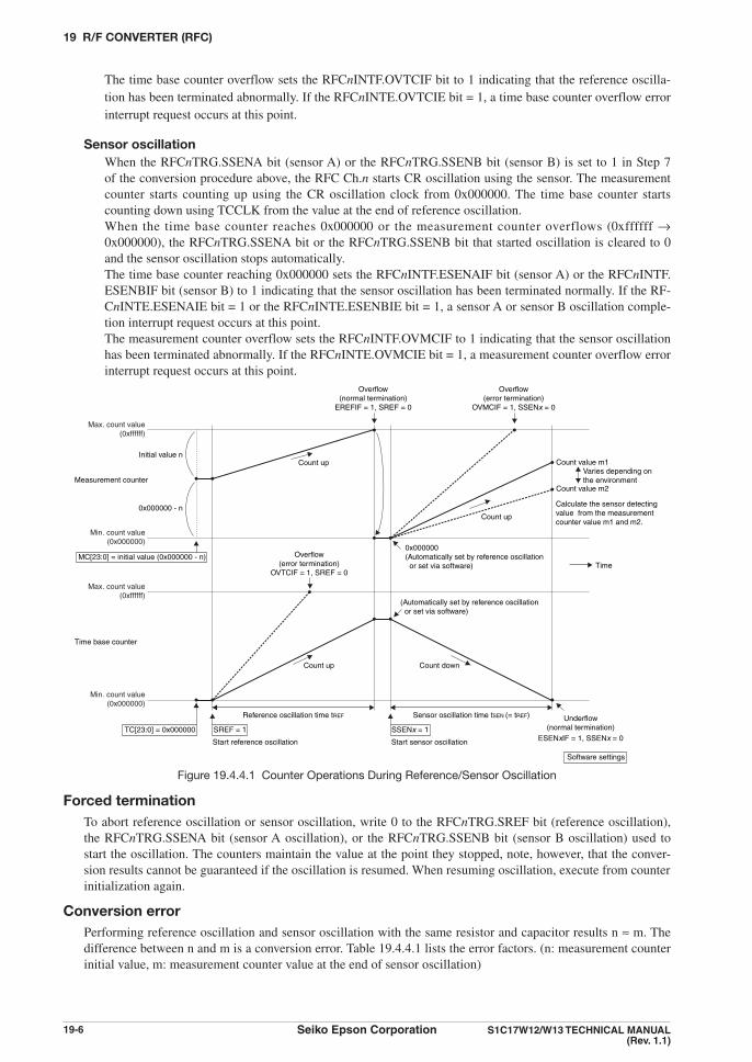
19 R/F CONVERTER (RFC)
19-6 Seiko Epson Corporation S1C17W12/W13 TECHNICAL MANUAL (Rev. 1.1)
The time base counter overflow sets the RFCnINTF.OVTCIF bit to 1 indicating that the reference oscilla-tion has been terminated abnormally. If the RFCnINTE.OVTCIE bit = 1, a time base counter overflow error interrupt request occurs at this point.
Sensor oscillation When the RFCnTRG.SSENA bit (sensor A) or the RFCnTRG.SSENB bit (sensor B) is set to 1 in Step 7
of the conversion procedure above, the RFC Ch.n starts CR oscillation using the sensor. The measurement counter starts counting up using the CR oscillation clock from 0x000000. The time base counter starts counting down using TCCLK from the value at the end of reference oscillation.
When the time base counter reaches 0x000000 or the measurement counter overflows (0xffffff → 0x000000), the RFCnTRG.SSENA bit or the RFCnTRG.SSENB bit that started oscillation is cleared to 0 and the sensor oscillation stops automatically.
The time base counter reaching 0x000000 sets the RFCnINTF.ESENAIF bit (sensor A) or the RFCnINTF.ESENBIF bit (sensor B) to 1 indicating that the sensor oscillation has been terminated normally. If the RF-CnINTE.ESENAIE bit = 1 or the RFCnINTE.ESENBIE bit = 1, a sensor A or sensor B oscillation comple-tion interrupt request occurs at this point.
The measurement counter overflow sets the RFCnINTF.OVMCIF to 1 indicating that the sensor oscillation has been terminated abnormally. If the RFCnINTE.OVMCIE bit = 1, a measurement counter overflow error interrupt request occurs at this point.
Max. count value(0xffffff)
Min. count value(0x000000)
Max. count value(0xffffff)
Min. count value(0x000000)
Overflow(normal termination)
EREFIF = 1, SREF = 0
Overflow(error termination)
OVMCIF = 1, SSENx = 0
Count value m1
Count value m2
Varies depending on the environment
Calculate the sensor detecting value from the measurement counter value m1 and m2.
Overflow(error termination)
OVTCIF = 1, SREF = 0
Underflow(normal termination)
ESENxIF = 1, SSENx = 0
0x000000(Automatically set by reference oscillation or set via software)
(Automatically set by reference oscillation or set via software)
Time
Reference oscillation time tREF Sensor oscillation time tSEN (= tREF)
Measurement counter
Time base counter
SREF = 1
Software settings
TC[23:0] = 0x000000
MC[23:0] = initial value (0x000000 - n)
SSENx = 1
Count up
Count up
Count up
Count down
Start sensor oscillationStart reference oscillation
Initial value n
0x000000 - n
Figure 19.4.4.1 Counter Operations During Reference/Sensor Oscillation
Forced termination To abort reference oscillation or sensor oscillation, write 0 to the RFCnTRG.SREF bit (reference oscillation),
the RFCnTRG.SSENA bit (sensor A oscillation), or the RFCnTRG.SSENB bit (sensor B oscillation) used to start the oscillation. The counters maintain the value at the point they stopped, note, however, that the conver-sion results cannot be guaranteed if the oscillation is resumed. When resuming oscillation, execute from counter initialization again.
Conversion error Performing reference oscillation and sensor oscillation with the same resistor and capacitor results n ≈ m. The
difference between n and m is a conversion error. Table 19.4.4.1 lists the error factors. (n: measurement counter initial value, m: measurement counter value at the end of sensor oscillation)

19 R/F CONVERTER (RFC)
S1C17W12/W13 TECHNICAL MANUAL Seiko Epson Corporation 19-7(Rev. 1.1)
Table 19.4.4.1 Error FactorsError factor Influence
External part tolerances LargePower supply voltage fluctuations LargeParasitic capacitance and resistance of the board MiddleTemperature SmallUnevenness of IC quality Small
19.4.5 CR Oscillation Frequency Monitoring FunctionThe CR oscillation clock (RFCLK) generated during converting operation can be output from the RFCLKOn pin for monitoring. By setting the RFCnCTL.CONEN bit to 1, the RFC Ch.n enters continuous oscillation mode that disables oscillation stop conditions to continue oscillating operations. In this case, set the the RFCnTRG.SREF bit (reference oscillation), the RFCnTRG.SSENA bit (sensor A oscillation), or the RFCnTRG.SSENB bit (sensor B os-cillation) to 1 to start oscillation. Set the bit to 0 to stop oscillation. Using this function helps easily measure the CR oscillation clock frequency. Furthermore, setting the RFCnCTL.RFCLKMD bit to 1 changes the output clock to the divided-by-two RFCLK clock.
RFINn pin
RFCLKOn pin(RFCnCTL.RFCLKMD = 0)
RFCLKOn pin(RFCnCTL.RFCLKMD = 1)
RFCnTRG.SSENA, SSENB, SREF
VDD
VSSVDD
VSS
RFCnCTL.CONEN
Writing 1 Writing 0
Figure 19.4.5.1 CR Oscillation Clock (RFCLK) Waveform
19.5 InterruptsThe RFC has a function to generate the interrupts shown in Table 19.5.1.
Table 19.5.1 RFC Interrupt Function
Interrupt Interrupt flag Set condition Clear condition
Reference oscillation completion
RFCnINTF.EREFIF When reference oscillation has been completed normally due to a measurement counter overflow
Writing 1
Sensor A oscillation completion
RFCnINTF.ESENAIF When sensor A oscillation has been completed normally due to the time base counter reaching 0x000000
Writing 1
Sensor B oscillation completion
RFCnINTF.ESENBIF When sensor B oscillation has been completed normally due to the time base counter reaching 0x000000
Writing 1
Measurement counter overflow error
RFCnINTF.OVMCIF When sensor oscillation has been terminated abnormally due to a measurement counter overflow
Writing 1
Time base counter overflow error
RFCnINTF.OVTCIF When reference oscillation has been terminated abnor-mally due to a time base counter overflow
Writing 1
The RFC provides interrupt enable bits corresponding to each interrupt flag. An interrupt request is sent to the in-terrupt controller only when the interrupt flag, of which interrupt has been enabled by the interrupt enable bit, is set. For more information on interrupt control, refer to the “Interrupt Controller” chapter.

19 R/F CONVERTER (RFC)
19-8 Seiko Epson Corporation S1C17W12/W13 TECHNICAL MANUAL (Rev. 1.1)
19.6 Control Registers
RFC Ch.n Clock Control RegisterRegister name Bit Bit name Initial Reset R/W Remarks
RFCnCLK 15–9 – 0x00 – R –8 DBRUN 1 H0 R/W
7–6 – 0x0 – R5–4 CLKDIV[1:0] 0x0 H0 R/W3–2 – 0x0 – R1–0 CLKSRC[1:0] 0x0 H0 R/W
Bits 15–9 Reserved
Bit 8 DBRUN This bit sets whether the RFC operating clock is supplied in DEBUG mode or not. 1 (R/W): Clock supplied in DEBUG mode 0 (R/W): No clock supplied in DEBUG mode
Bits 7–6 Reserved
Bits 5–4 CLKDIV[1:0] These bits select the division ratio of the RFC operating clock.
Bits 3–2 Reserved
Bits 1–0 CLKSRC[1:0] These bits select the clock source of the RFC.
Table 19.6.1 Clock Source and Division Ratio Settings
RFCnCLK.CLKDIV[1:0] bits
RFCnCLK.CLKSRC[1:0] bits0x0 0x1 0x2 0x3
IOSC OSC1 OSC3 EXOSC0x3 1/8 1/1 1/8 1/10x2 1/4 1/40x1 1/2 1/20x0 1/1 1/1
(Note) The oscillation circuits/external input that are not supported in this IC cannot be selected as the clock source.
Note: The RFCnCLK register settings can be altered only when the RFCnCTL.MODEN bit = 0.
RFC Ch.n Control RegisterRegister name Bit Bit name Initial Reset R/W Remarks
RFCnCTL 15–9 – 0x00 – R –8 RFCLKMD 0 H0 R/W7 CONEN 0 H0 R/W6 EVTEN 0 H0 R/W
5–4 SMODE[1:0] 0x0 H0 R/W3–1 – 0x0 – R0 MODEN 0 H0 R/W
Bits 15–9 Reserved
Bit 8 RFCLKMD This bit sets the RFCLKOn pin to output the divided-by-two oscillation clock. 1 (R/W): Divided-by-two clock output 0 (R/W): Oscillation clock output
For more information, refer to “CR Oscillation Frequency Monitoring Function.”

19 R/F CONVERTER (RFC)
S1C17W12/W13 TECHNICAL MANUAL Seiko Epson Corporation 19-9(Rev. 1.1)
Bit 7 CONEN This bit disables the automatic CR oscillation stop function to enable continuous oscillation function. 1 (R/W): Enable continuous oscillation 0 (R/W): Disable continuous oscillation
For more information, refer to “CR Oscillation Frequency Monitoring Function.”
Bit 6 EVTEN This bit enables external clock input mode (event counter mode). 1 (R/W): External clock input mode 0 (R/W): Normal mode
For more information, refer to “Operating Modes.”
Note: Do not input an external clock before the RFCnCTL.EVTEN bit is set to 1. The RFINn pin is pulled down to VSS level when the port function is switched for the R/F converter.
Bits 5–4 SMODE[1:0] These bits configure the oscillation mode. For more information, refer to “Operating Modes.”
Table 19.6.2 Oscillation Mode SelectionRFCnCTL.SMODE[1:0] bits Oscillation mode
0x3, 0x2 Reserved0x1 AC oscillation mode for resistive sensor measurements0x0 DC oscillation mode for resistive sensor measurements
Bits 3–1 Reserved
Bit 0 MODEN This bit enables the RFC operations. 1 (R/W): Enable RFC operations (The operating clock is supplied.) 0 (R/W): Disable RFC operations (The operating clock is stopped.)
Note: If the RFCnCTL.MODEN bit is altered from 1 to 0 during R/F conversion, the counter value being converted cannot be guaranteed. R/F conversion cannot be resumed.
RFC Ch.n Oscillation Trigger RegisterRegister name Bit Bit name Initial Reset R/W Remarks
RFCnTRG 15–8 – 0x00 – R –7–3 – 0x00 – R2 SSENB 0 H0 R/W1 SSENA 0 H0 R/W0 SREF 0 H0 R/W
Bits 15–3 Reserved
Bit 2 SSENB This bit controls CR oscillation for sensor B. This bit also indicates the CR oscillation status. 1 (W): Start oscillation 0 (W): Stop oscillation 1 (R): Being oscillated 0 (R): Stopped
Note: Writing 1 to the RFCnTRG.SSENB bit does not start oscillation when the RFCnCTL.SMODE[1:0] bits = 0x1 (AC oscillation mode for resistive sensor measurements).
Bit 1 SSENA This bit controls CR oscillation for sensor A. This bit also indicates the CR oscillation status. 1 (W): Start oscillation 0 (W): Stop oscillation 1 (R): Being oscillated 0 (R): Stopped

19 R/F CONVERTER (RFC)
19-10 Seiko Epson Corporation S1C17W12/W13 TECHNICAL MANUAL (Rev. 1.1)
Bit 0 SREF This bit controls CR oscillation for the reference resistor. This bit also indicates the CR oscillation sta-
tus. 1 (W): Start oscillation 0 (W): Stop oscillation 1 (R): Being oscillated 0 (R): Stopped
Notes: • Settings in this register are all ineffective when the RFCnCTL.MODEN bit = 0 (RFC operation disabled).
• When writing 1 to the RFCnTRG.SREF bit, the RFCnTRG.SSENA bit, or the RFCnTRG.SSENB bit to start oscillation, be sure to avoid having more than one bit set to 1.
• Be sure to clear the interrupt flags (RFCnINTF.EREFIF bit, RFCnINTF.ESENAIF bit, RFCnINTF.ESENBIF bit, RFCnINTF.OVMCIF bit, and RFCnINTF.OVTCIF bit) before starting oscillation using this register.
RFC Ch.n Measurement Counter Low and High RegistersRegister name Bit Bit name Initial Reset R/W Remarks
RFCnMCL 15–0 MC[15:0] 0x0000 H0 R/W –RFCnMCH 15–8 – 0x00 – R –
7–0 MC[23:16] 0x00 H0 R/WOr
Register name Bit Bit name Initial Reset R/W Remarks
RFCnMCLRFCnMCH
31–24 – 0x00 – R –23–0 MC[23:0] 0x000000 H0 R/W
Bits 31–24 Reserved
Bits 23–0 MC[23:0] Measurement counter data can be read and written through these bits.
Note: The measurement counter must be set from the low-order value (RFCnMCL.MC[15:0] bits) first when data is set using a 16-bit access instruction. The counter may not be set to the correct value if the high-order value (RFCnMCH.MC[23:16] bits) is written first.
RFC Ch.n Time Base Counter Low and High RegistersRegister name Bit Bit name Initial Reset R/W Remarks
RFCnTCL 15–0 TC[15:0] 0x0000 H0 R/W –RFCnTCH 15–8 – 0x00 – R –
7–0 TC[23:16] 0x00 H0 R/WOr
Register name Bit Bit name Initial Reset R/W Remarks
RFCnTCLRFCnTCH
31–24 – 0x00 – R –23–0 TC[23:0] 0x000000 H0 R/W
Bits 31–24 Reserved
Bits 23–0 TC[23:0] Time base counter data can be read and written through these bits.
Note: The time base counter must be set from the low-order value (RFCnTCL.TC[15:0] bits) first when data is set using a 16-bit access instruction. The counter may not be set to the correct value if the high-order value (RFCnTCH.TC[23:16] bits) is written first.
19 R/F CONVERTER (RFC)
S1C17W12/W13 TECHNICAL MANUAL Seiko Epson Corporation 19-11(Rev. 1.1)
RFC Ch.n Interrupt Flag RegisterRegister name Bit Bit name Initial Reset R/W Remarks
RFCnINTF 15–8 – 0x00 – R –7–5 – 0x0 – R4 OVTCIF 0 H0 R/W Cleared by writing 1.3 OVMCIF 0 H0 R/W2 ESENBIF 0 H0 R/W1 ESENAIF 0 H0 R/W0 EREFIF 0 H0 R/W
Bits 15–5 Reserved
Bit 4 OVTCIFBit 3 OVMCIFBit 2 ESENBIFBit 1 ESENAIFBit 0 EREFIF These bits indicate the RFC interrupt cause occurrence status. 1 (R): Cause of interrupt occurred 0 (R): No cause of interrupt occurred 1 (W): Clear flag 0 (W): Ineffective
The following shows the correspondence between the bit and interrupt: RFCnINTF.OVTCIF bit: Time base counter overflow error interrupt RFCnINTF.OVMCIF bit: Measurement counter overflow error interrupt RFCnINTF.ESENBIF bit: Sensor B oscillation completion interrupt RFCnINTF.ESENAIF bit: Sensor A oscillation completion interrupt RFCnINTF.EREFIF bit: Reference oscillation completion interrupt
RFC Ch.n Interrupt Enable RegisterRegister name Bit Bit name Initial Reset R/W Remarks
RFCnINTE 15–8 – 0x00 – R –7–5 – 0x0 – R4 OVTCIE 0 H0 R/W3 OVMCIE 0 H0 R/W2 ESENBIE 0 H0 R/W1 ESENAIE 0 H0 R/W0 EREFIE 0 H0 R/W
Bits 15–5 Reserved
Bit 4 OVTCIEBit 3 OVMCIEBit 2 ESENBIEBit 1 ESENAIEBit 0 EREFIE These bits enable RFC interrupts. 1 (R/W): Enable interrupts 0 (R/W): Disable interrupts
The following shows the correspondence between the bit and interrupt: RFCnINTE.OVTCIE bit: Time base counter overflow error interrupt RFCnINTE.OVMCIE bit: Measurement counter overflow error interrupt RFCnINTE.ESENBIE bit: Sensor B oscillation completion interrupt RFCnINTE.ESENAIE bit: Sensor A oscillation completion interrupt RFCnINTE.EREFIE bit: Reference oscillation completion interrupt

20 Multiplier/Divider (COPRO2)
S1C17W12/W13 TECHNICAL MANUAL Seiko Epson Corporation 20-1(Rev. 1.1)
20 Multiplier/Divider (COPRO2)
20.1 OverviewCOPRO2 is the coprocessor that provides multiplier/divider functions. The features of COPRO2 are listed below.
• Multiplication: Supports signed/unsigned multiplications. (16 bits × 16 bits = 32 bits) Can be executed in 1 cycle.
• Multiplication and accumulation (MAC): Supports signed/unsigned MAC operations with overflow detection function. (16 bits × 16 bits + 32 bits = 32 bits) Can be executed in 1 cycle.
• Division: Supports signed/unsigned divisions. (32 bits ÷ 32 bits = 32 bits with 32-bit reminder) Can be executed in 17 to 20 cycles. Overflow detection and division by zero processing are not supported.
Figure 20.1.1 shows the COPRO2 configuration.
S1C17 Core
Arithmetic unit
Operation result register 0
Operation result register 1
Mode setting
Selector
Argument 2
Argument 1
Coprocessoroutput
Flag output
Operation result
COPRO2
Figure 20.1.1 COPRO2 Configuration
20.2 Operation Mode and Output ModeCOPRO2 operates according to the operation mode specified by the application program. As listed in Table 20.2.1, COPRO2 supports 11 operations.The multiplication, division and MAC results are 32-bit data, therefore, the S1C17 Core cannot read them in one access cycle. The output mode is provided to specify the high-order 16 bits or low-order 16 bits of the operation result register 0 or 1 to be read from COPRO2.The operation and output modes can be specified with a 7-bit data by writing it to the mode setting register in COPRO2. Use a “ld.cw” instruction for this writing.
ld.cw %rd,%rs %rs[6:0] is written to the mode setting register. (%rd: not used) ld.cw %rd,imm7 imm7[6:0] is written to the mode setting register. (%rd: not used)
6 4 3 0Output mode setting value Operation mode setting value
Figure 20.2.1 Mode Setting Register

20 Multiplier/Divider (COPRO2)
20-2 Seiko Epson Corporation S1C17W12/W13 TECHNICAL MANUAL (Rev. 1.1)
Table 20.2.1 Mode SettingsSetting value
(D[6:4])Output mode
Setting value
(D[3:0])Operation mode
0x0 16 low-order bits output mode 0The low-order 16 bits of the operation result reg-ister 0 can be read as the coprocessor output.
0x0 Initialize mode 0Clears the operation result registers 0 and 1 to 0x0.
0x1 16 high-order bits output mode 0The high-order 16 bits of the operation result reg-ister 0 can be read as the coprocessor output.
0x1 Initialize mode 1Loads the 16-bit augend into the low-order 16 bits of the operation result register 0.
0x2 16 low-order bits output mode 1The low-order 16 bits of the operation result reg-ister 1 can be read as the coprocessor output.
0x2 Initialize mode 2Loads the 32-bit data into the operation re-sult register 0.
0x3 16 high-order bits output mode 1The high-order 16 bits of the operation result reg-ister 1 can be read as the coprocessor output.
0x3 Operation result read modeOutputs the data in the operation result reg-isters 0 and 1 without computation.
0x4–0x7 Reserved 0x4 Unsigned multiplication modePerforms unsigned multiplication.
0x5 Signed multiplication modePerforms signed multiplication.
0x6 Unsigned MAC modePerforms unsigned MAC operation.
0x7 Signed MAC modePerforms signed MAC operation.
0x8 Unsigned division modePerforms unsigned division.
0x9 Signed division modePerforms signed division.
0xa Initialize mode 3Loads the 32-bit data into the operation re-sult register 1.
0xb–0xf Reserved
20.3 MultiplicationThe multiplication function performs “A (32 bits) = B (16 bits) × C (16 bits).”The following shows a procedure to perform a multiplication:
1. Set the mode to 0x04 (unsigned multiplication, 16 low-order bits output mode 0) or 0x05 (signed multiplica-tion, 16 low-order bits output mode 0).
2. Send the 16-bit multiplicand (B) and 16-bit multiplier (C) to COPRO2 using a “ld.ca” instruction.
3. Read the one-half result (16 low-order bits = A[15:0]) and the flag status.
4. Set the mode to 0x13 (operation result read, 16 high-order bits output mode 0).
5. Read another one-half result (16 high-order bits = A[31:16]).
16 bits
32 bits
S1C17 Core
Operation result register 0
Operation result register 1
Selector
Argument 2
Argument 1
Coprocessoroutput (16 bits)
Flag output
Operation result
COPRO2
Figure 20.3.1 Data Path in Multiplication Mode

20 Multiplier/Divider (COPRO2)
S1C17W12/W13 TECHNICAL MANUAL Seiko Epson Corporation 20-3(Rev. 1.1)
Table 20.3.1 Operation in Multiplication ModeMode set-ting value Instruction Operations Flags Remarks
0x04 or 0x05
ld.ca %rd,%rs res0[31:0] ← %rd × %rs%rd ← res0[15:0]
psr (CVZN) ← 0b0000 The operation result register 0 keeps the operation result until it is rewritten by other operation.
(ext imm9) ld.ca %rd,imm7
res0[31:0] ← %rd × imm7/16%rd ← res0[15:0]
0x14 or 0x15
ld.ca %rd,%rs res0[31:0] ← %rd × %rs %rd ← res0[31:16]
(ext imm9) ld.ca %rd,imm7
res0[31:0] ← %rd × imm7/16 %rd ← res0[31:16]
res0: operation result register 0Example:
ld.cw %r0,0x04 ; Sets the mode (unsigned multiplication mode and 16 low-order bits output mode 0).ld.ca %r0,%r1 ; Performs “res0[31:0] = %r0[15:0] × %r1[15:0]” and loads the 16 low-order bits of the
result to %r0.ld.cw %r0,0x13 ; Sets the mode (operation result read mode and 16 high-order bits output mode 0).ld.ca %r1,%r0 ; Loads the 16 high-order bits of the result to %r1.
20.4 DivisionThe division function performs “A (32 bits) = B (32 bits) ÷ C (32 bits), D (32 bits) = remainder.”The following shows a procedure to perform a division:
1. Set the mode to 0x02 (initialize mode 2).
2 Set the 32-bit dividend (B) to the operation result register 0 using a “ld.cf” instruction.
3. Set the mode to 0x08 (unsigned division, 16 low-order bits output mode 0) or 0x09 (signed division, 16 low-order bits output mode 0).
4. Send the 32-bit divisor (C) to COPRO2 using a “ld.ca” instruction.
5. Read the one-half result (16 low-order bits = A[15:0]) of the operation result register 0 (quotient) and the flag status.
6. Set the mode to 0x13 (operation result read, 16 high-order bits output mode 0).
7. Read another one-half result (16 high-order bits = A[31:16]) of the operation result register 0 (quotient).
8. Set the mode to 0x23 (operation result read, 16 low-order bits output mode 1).
9. Read the one-half result (16 low-order bits = D[15:0]) of the operation result register 1 (remainder).
10. Set the mode to 0x33 (operation result read, 16 high-order bits output mode 1).
11. Read another one-half result (16 high-order bits = D[31:16]) of the operation result register 1 (remainder).
16 bits
32 bits
S1C17 Core
Operation result register 0
Operation result register 1
Selector
Argument 2
Argument 1
Coprocessoroutput
Flag output
Operation result
COPRO2
Figure 20.4.1 Data Path in Initialize Mode 2

20 Multiplier/Divider (COPRO2)
20-4 Seiko Epson Corporation S1C17W12/W13 TECHNICAL MANUAL (Rev. 1.1)
Table 20.4.1 Initializing the Operation Result Register 0 (32 bits)Mode set-ting value Instruction Operations Remarks
0x02 ld.cf %rd,%rs res0[31:16] ← %rd res0[15:0] ← %rs
(ext imm9) ld.cf %rd,imm7
res0[31:16] ← %rd res0[15:0] ← imm7/16
res0: operation result register 0
÷
16 bits
32 bits
32 bits
S1C17 Core
Operation result register 0
Operation result register 1
Selector
Argument 2
Argument 1
Coprocessoroutput (16 bits)
Flag output
QuotientRemainder
COPRO2
Figure 20.4.2 Data Path in Division Mode
Table 20.4.2 Operation in Division ModeMode set-ting value Instruction Operations Flags Remarks
0x08 or 0x09
ld.ca %rd,%rs res0[31:0] ÷%rd, %rsres0[31:0] ← Quotientres1[31:0] ← Remainder%rd ← res0[15:0] (Quotient)
psr (CVZN) ← 0b0000 The operation result regis-ters 0 and 1 keep the op-eration results until they are rewritten by other opera-tion.
COPRO2 does not support 0 ÷ 0 division.
(ext imm9) ld.ca %rd,imm7
res0[31:0] ÷%rd, imm7/16res0[31:0] ← Quotientres1[31:0] ← Remainder%rd ← res0[15:0] (Quotient)
0x18 or 0x19
ld.ca %rd,%rs res0[31:0] ÷%rd, %rsres0[31:0] ← Quotientres1[31:0] ← Remainder%rd ← res0[31:16] (Quotient)
(ext imm9) ld.ca %rd,imm7
res0[31:0] ÷%rd, imm7/16res0[31:0] ← Quotientres1[31:0] ← Remainder%rd ← res0[31:16] (Quotient)
0x28 or 0x29
ld.ca %rd,%rs res0[31:0] ÷%rd, %rsres0[31:0] ← Quotientres1[31:0] ← Remainder%rd ← res1[15:0] (Remainder)
(ext imm9) ld.ca %rd,imm7
res0[31:0] ÷%rd, imm7/16res0[31:0] ← Quotientres1[31:0] ← Remainder%rd ← res1[15:0] (Remainder)
0x38 or 0x39
ld.ca %rd,%rs res0[31:0] ÷%rd, %rsres0[31:0] ← Quotientres1[31:0] ← Remainder%rd ← res1[31:16] (Remainder)
(ext imm9) ld.ca %rd,imm7
res0[31:0] ÷%rd, imm7/16res0[31:0] ← Quotientres1[31:0] ← Remainder%rd ← res1[31:16] (Remainder)
res0: operation result register 0, res1: operation result register 1

20 Multiplier/Divider (COPRO2)
S1C17W12/W13 TECHNICAL MANUAL Seiko Epson Corporation 20-5(Rev. 1.1)
Example:ld.cw %r0,0x02 ; Sets the mode (initialize mode 2).ld.cf %r0,%r1 ; Set the dividend %r0, %r1 to the operation result register 0.ld.cw %r0,0x08 ; Sets the mode (unsigned division mode and 16 low-order bits output mode 0).ld.ca %r0,%r1 ; Performs “res0[31:0] (quotient), res1[31:0] (remainder) = res0[31:0] ÷ %r0[15:0],
%r1[15:0]” and loads the 16 low-order bits of the result (quotient) to %r0.ld.ca %r1,%r0 ; Loads the 16 low-order bits of the result (quotient) to %r1.ld.cw %r0,0x13 ; Sets the mode (operation result read mode and 16 high-order bits output mode 0).ld.ca %r2,%r0 ; Loads the 16 high-order bits of the result (quotient) to %r2.ld.cw %r0,0x23 ; Sets the mode (operation result read mode and 16 low-order bits output mode 1).ld.ca %r3,%r0 ; Loads the 16 low-order bits of the result (remainder) to %r3.ld.cw %r0,0x33 ; Sets the mode (operation result read mode and 16 high-order bits output mode 1).ld.ca %r4,%r0 ; Loads the 16 high-order bits of the result (remainder) to %r4.
20.5 MACThe MAC (multiplication and accumulation) function performs “A (32 bits) = B (16 bits) × C (16 bits) + A (32 bits).”The following shows a procedure to perform a MAC operation:
1. Set the initial value (A) to the operation result register 0.• To clear the operation result registers (A = 0): Set the mode to 0x00 (initialize mode 0). (It is not necessary to send 0x00 to COPRO2 with another instruc-
tion.)• To load a 16-bit value to the operation result register 0: Set the operation mode to 0x01 (initialize mode 1) and then send the initial value (16 bits) to COPRO2 us-
ing a “ld.cf” instruction.• To load a 32-bit value to the operation result register 0: Set the operation mode to 0x02 (initialize mode 2) and then send the initial value (32 bits) to COPRO2 us-
ing a “ld.cf” instruction.
2. Set the mode to 0x06 (unsigned MAC, 16 low-order bits output mode 0) or 0x07 (signed MAC, 16 low-order bits output mode 0).
3. Repeat sending the 16-bit multiplicand (B) and 16-bit multiplier (C) to COPRO2 the number of times required using a “ld.ca” instruction.
4. Read the one-half result (16 low-order bits = A[15:0]) and the flag status.
5. Set the mode to 0x13 (operation result read, 16 high-order bits output mode).
6. Read another one-half result (16 high-order bits = A[31:16]).
16 bits
32 bits
S1C17 Core
Operation result register 0
Operation result register 1
Selector
Argument 2
Argument 1
Coprocessoroutput
Flag output
COPRO2
Figure 20.5.1 Data Path in Initialize Mode

20 Multiplier/Divider (COPRO2)
20-6 Seiko Epson Corporation S1C17W12/W13 TECHNICAL MANUAL (Rev. 1.1)
Table 20.5.1 Initializing the Operation Result Register 0Mode set-ting value Instruction Operations Remarks
0x00 – res0[31:0] ← 0x0res1[31:0] ← 0x0
Setting the operating mode executes the initialization without sending data.
0x01 ld.cf %rd,%rs res0[31:16] ← 0x0 res0[15:0] ← %rs
(ext imm9) ld.cf %rd,imm7
res0[31:16] ← 0x0 res0[15:0] ← imm7/16
0x02 ld.cf %rd,%rs res0[31:16] ← %rd res0[15:0] ← %rs
(ext imm9) ld.cf %rd,imm7
res0[31:16] ← %rd res0[15:0] ← imm7/16
res0: operation result register 0, res1: operation result register 1
32 bits
16 bits32 bits
S1C17 Core
Operation result register 0
Operation result register 1
Selector
Argument 2
Argument 1
Coprocessoroutput (16 bits)
Flag output
Operation result
COPRO2
Figure 20.5.2 Data Path in MAC Mode
Table 20.5.2 Operation in MAC ModeMode set-ting value Instruction Operations Flags Remarks
0x06or 0x07
ld.ca %rd,%rs res0[31:0] ← %rd × %rs + res0[31:0]%rd ← res0[15:0]
psr (CVZN) ← 0b0100 if an overflow has oc-curred
Otherwise psr (CVZN) ← 0b0000
The operation result register 0 keeps the operation result until it is rewritten by other operation.Overflow can be de-tected only in signed MAC mode (it does not occur in unsigned MAC mode).
(ext imm9) ld.ca %rd,imm7
res0[31:0] ← %rd × imm7/16 + res0[31:0]%rd ← res0[15:0]
0x16or 0x17
ld.ca %rd,%rs res0[31:0] ← %rd × %rs + res0[31:0]%rd ← res0[31:16]
(ext imm9) ld.ca %rd,imm7
res0[31:0] ← %rd × imm7/16 + res0[31:0]%rd ← res0[31:16]
res0: operation result register 0
Example:ld.cw %r0,0x00 ; Sets the mode (initialize mode 0) to clear the operation result register 0 to 0x0000.ld.cw %r0,0x07 ; Sets the mode (signed MAC mode and 16 low-order bits output mode 0).ld.ca %r0,%r1 ; Performs “res0[31:0] = %r0[15:0] × %r1[15:0] + res0[31:0]” and loads the 16 low-
order bits of the result to %r0.ld.cw %r0,0x13 ; Sets the mode (operation result read mode and 16 high-order bits output mode 0).ld.ca %r1,%r0 ; Loads the 16 high-order bits of the result to %r1.

20 Multiplier/Divider (COPRO2)
S1C17W12/W13 TECHNICAL MANUAL Seiko Epson Corporation 20-7(Rev. 1.1)
Conditions to set the overflow (V) flag An overflow occurs in a signed MAC operation and the overflow (V) flag is set to 1 when the signs of the mul-
tiplication result, operation result register value, and multiplication & accumulation result match the following conditions:
Table 20.5.3 Conditions to Set the Overflow (V) Flag
Mode setting value Sign of multiplication result Sign of operation result register value
Sign of multiplication & accumulation result
0x07 0 (positive) 0 (positive) 1 (negative)0x07 1 (negative) 1 (negative) 0 (positive)
An overflow occurs when a MAC operation performs addition of positive values and a negative value results, or it performs addition of negative values and a positive value results. The coprocessor holds the operation result until the overflow (V) flag is cleared.
Conditions to clear the overflow (V) flag The overflow (V) flag that has been set will be cleared when an overflow has not been occurred during execu-
tion of the “ld.ca” instruction for MAC operation or when the “ld.ca” or “ld.cf” instruction is executed in an operation mode other than operation result read mode.
20.6 Reading Operation ResultsThe “ld.ca” instruction cannot load a 32-bit operation result to a CPU register, so a multiplication, division or MAC operation returns the one-half (16 bits according to the output mode) result (A[15:0] or A[31:16]) and the flag status to the CPU registers. Another one-half should be read by setting COPRO2 into operation result read mode. The operation result register keeps the loaded operation result until it is rewritten by other operation.
16 bits
S1C17 Core
Operation result register 0
Operation result register 1
Selector
Argument 2
Argument 1
Coprocessoroutput (16 bits)
Flag output
COPRO2
Figure 20.6.1 Data Path in Operation Result Read Mode
Table 20.6.1 Operation in Operation Result Read ModeMode set-ting value Instruction Operations Flags Remarks
0x03 ld.ca %rd,%rs %rd ← res[15:0] psr (CVZN) ← 0b0000 This operation mode does not affect the operation result reg-isters 0 and 1.
ld.ca %rd,imm7 %rd ← res[15:0]0x13 ld.ca %rd,%rs %rd ← res[31:16]
ld.ca %rd,imm7 %rd ← res[31:16]0x23 ld.ca %rd,%rs %rd ← res1[15:0]
ld.ca %rd,imm7 %rd ← res1[15:0]0x33 ld.ca %rd,%rs %rd ← res1[31:16]
ld.ca %rd,imm7 %rd ← res1[31:16]res0: operation result register 0, res1: operation result register 1

21 ELECTRICAL CHARACTERISTICS
S1C17W12/W13 TECHNICAL MANUAL Seiko Epson Corporation 21-1(Rev. 1.1)
21 Electrical Characteristics21.1 Absolute Maximum Ratings
(VSS = 0 V)Item Symbol Condition Rated value Unit
Power supply voltage VDD -0.3 to 4.0 VFlash programming voltage VPP -0.3 to 8.0 VLCD power supply voltage VC1 -0.3 to 7.0 V
VC2 -0.3 to 7.0 VVC3 -0.3 to 7.0 V
Input voltage VI P04–07, PD3–D4 -0.3 to VDD + 0.5 VP00–03, P10–17, P20–26, P40–43, PD0–D1 -0.3 to 4.0 V
Output voltage VO P00–07, P10–17, P20–26, P40–43, PD0–D4 -0.3 to VDD + 0.5 VHigh level output current IOH 1 pin P00–07, P10–17, P20–26, P40–43, PD0–D4 -10 mA
Total of all pins -20 mALow level output current IOL 1 pin P00–07, P10–17, P20–26, P40–43, PD0–D4 10 mA
Total of all pins 20 mAOperating temperature Ta -40 to 85 °CStorage temperature Tstg -65 to 125 °C
21.2 Recommended Operating ConditionsItem Symbol Condition Min. Typ. Max. Unit
Power supply voltage VDD For normal operation 1.2 – 3.6 VFor Flash programming 2.4 – 3.6 VFor super economy mode 2.5 – 3.6 V
Flash programming voltage VPP 7.3 7.5 7.7 VLCD power supply voltage VC1 When an external voltage is applied
VC1 ≤ VDD ≤ VC2 ≤ VC3
– 1.0 1.8 VVC2 – 2.0 3.6 VVC3 – 3.0 5.4 V
OSC1 oscillator oscillation frequency fOSC1 Crystal oscillator – 32.768 – kHzOSC3 oscillator oscillation frequency fOSC3 Internal oscillator or crystal/
ceramic oscillatorVDD = 1.2 to 1.6 V 0.5 – 1.1 MHzVDD = 1.6 to 3.6 V 0.5 – 4.2 MHz
CR oscillator VDD = 1.6 to 3.6 V 0.1 – 2.1 MHzEXOSC external clock frequency fEXOSC When supplied from an
external oscillatorVDD = 1.2 to 1.6 V 0.016 – 1.1 MHzVDD = 1.6 to 3.6 V 0.016 – 4.2 MHz
Bypass capacitor between VSS and VDD CPW1 – 3.3 – µFCapacitors between VSS and VD1–2 CPW2–3 – 1 – µFCapacitor between CV1 and CV2 CCV *1 – 1 10 µFCapacitors between VSS and VC1–3 CLCD1–3 *2 – 1 – µFCapacitor between CP1 and CP2 CLCD5 *2 – 1 – µFGate capacitor for OSC1 oscillator CG1 *3 0 – 25 pFDrain capacitor for OSC1 oscillator CD1 *3 – 0 – pFGate capacitor for OSC3 oscillator CG3 When the crystal/ceramic oscillator is used *3 0 – 100 pFDrain capacitor for OSC3 oscillator CD3 When the crystal/ceramic oscillator is used *3 0 – 100 pFOscillation resistor for OSC3 oscillator RCR3 When the CR oscillator is used 10 – 1,000 kWDSIO pull-up resistor RDBG *4 – 10 – kWCapacitor between VSS and VPP CVPP – 0.1 – µF*1 The CV1–CV2 pins can be left open when super economy mode is not used.*2 The VC1–VC3 and CP1–CP2 pins can be left open when the LCD driver is not used.*3 The component values should be determined after performing matching evaluation of the resonator mounted on the printed cir-
cuit board actually used.*4 RDBG is not required when using the DSIO pin as a general-purpose I/O port.

21 ELECTRICAL CHARACTERISTICS
21-2 Seiko Epson Corporation S1C17W12/W13 TECHNICAL MANUAL (Rev. 1.1)
21.3 Current ConsumptionUnless otherwise specified: VDD = 1.2 to 3.6 V, VSS = 0 V, Ta = 25 °C, EXOSC = OFF, PWGCTL.PWGMOD[2:0] bits = 0x0 (automatic mode), PWGTIM.DCCCLK[1:0] bits = 0x0 (1/32), FLASHCWAIT.RDWAIT[1:0] bits = 0x1 (2 cycles)
Item Symbol Condition VDD or Ta Min. Typ. Max. UnitCurrent consumption in SLEEP mode
ISLP IOSC = OFF, OSC1 = OFF, OSC3 = OFF 25 °C – 0.15 0.5 µA85 °C – 0.8 9.0 µA
Current consumption in HALT mode
IHALT1 IOSC = ON, OSC1 = 32.768 kHz*1, OSC3 = OFF – 30 50 µAIHALT2 IOSC = OFF, OSC1 = 32.768 kHz*1, OSC3 = OFF – 0.5 1.6 µA
IOSC = OFF, OSC1 = 32.768 kHz*1, OSC3 = OFF, PWGCTL.PWGMOD[2:0] bits = 0x5 (super economy mode)
2.5 to 3.6 V – 0.3 0.9 µA
IOSC = OFF, OSC1 = 32 kHz*2, OSC3 = OFF – 1.5 4.0 µAIHALT3 IOSC = OFF, OSC1 = 32.768 kHz*1, OSC3 = 1 MHz (ceramic oscillator)*3 – 25 45 µA
Current consumption in RUN mode
IRUN1*6 IOSC = ON, OSC1 = 32.768 kHz*1, OSC3 = OFF, SYSCLK = IOSC – 110 200 µAIOSC = ON, OSC1 = 32.768 kHz*1, OSC3 = OFF, SYSCLK = IOSCFLASHCWAIT.RDWAIT[1:0] bits = 0x0 (1 cycle)
– 130 300 µA
IRUN2*6 IOSC = OFF, OSC1 = 32.768 kHz*1, OSC3 = OFF, SYSCLK = OSC1 – 4 9 µAIOSC = OFF, OSC1 = 32.768 kHz*1, OSC3 = OFF, SYSCLK = OSC1PWGCTL.PWGMOD[2:0] bits = 0x2 (normal mode)
– 13 22 µA
IOSC = OFF, OSC1 = 32.768 kHz*1, OSC3 = OFF, SYSCLK = OSC1, PWGCTL.PWGMOD[2:0] bits = 0x5 (super economy mode)
2.5 to 3.6 V – 2 6 µA
IRUN3*6 IOSC = OFF, OSC1 = 32.768 kHz*1, OSC3 = 1 MHz (ceramic oscillator)*3, SYSCLK = OSC3
– 140 250 µA
IOSC = OFF, OSC1 = 32.768 kHz*1, OSC3 = 1 MHz (CR oscillator)*4, SYSCLK = OSC3
1.6 to 3.6 V – 210 300 µA
IOSC = OFF, OSC1 = 32.768 kHz*1, OSC3 = 4 MHz (internal oscillator)*5, SYSCLK = OSC3
– 500 1,000 µA
*1 OSC1 oscillator: CLGOSC1.OSC1SELCR bit = 0, CLGOSC1.INV1N[1:0] bits = 0x0, CLGOSC1.CGI1[2:0] bits = 0x0, CLGOSC1.OSDEN bit = 0, CG1 = CD1 = 0 pF, Crystal resonator = C-002RX (manufactured by Seiko Epson Corporation, R1 = 50 kW (Max.), CL = 7 pF)
*2 OSC1 oscillator: CLGOSC1.OSC1SELCR bit = 1*3 OSC3 oscillator: CLGOSC3.OSC3MD[1:0] bits = 0x2, CLGOSC3.OSC3INV[1:0] bits = 0x0, CG3 = CD3 = 100 pF, ceramic resonator
= CSBLA_J (manufactured by Murata Manufacturing Co., Ltd., 1 MHz)*4 OSC3 oscillator: CLGOSC3.OSC3MD[1:0] bits = 0x1, RCR3 = 68 kW*5 OSC3 oscillator: CLGOSC3.OSC3MD[1:0] bits = 0x0, CLGOSC3.OSC3FQ[2:0] bits = 0x3*6 The current consumption values were measured when a test program consisting of 60.5 % ALU instructions, 17 % branch instruc-
tions, 12 % RAM read instructions, and 10.5 % RAM write instructions was executed continuously in the Flash memory.
Current consumption-temperature characteristicin SLEEP modeIOSC = OFF, OSC1 = OFF, OSC3 = OFF, Typ. value
-50
0.9
0.8
0.7
0.6
0.5
0.4
0.3
0.2
0.1
0.0-25 0 25 50 75 100
Ta [°C]
ISLP
[µA
]

21 ELECTRICAL CHARACTERISTICS
S1C17W12/W13 TECHNICAL MANUAL Seiko Epson Corporation 21-3(Rev. 1.1)
Current consumption-temperature characteristic Current consumption-temperature characteristicin HALT mode (IOSC operation) in HALT mode (OSC1 operation)IOSC = ON, OSC1 = 32.768 kHz, OSC3 = OFF, Typ. value IOSC = OFF, OSC1 = 32.768 kHz, OSC3 = OFF, Typ. value
-50
60
50
40
30
20
10
0-25 0 25 50 75 100
Ta [°C]
IHA
LT1
[µA
]
-50
2.5
2.0
1.5
1.0
0.5
0.0-25 0 25 50 75 100
Ta [°C]
IHA
LT2
[µA
]
Economy mode
Super economy mode
Current consumption-temperature characteristic Current consumption-temperature characteristicin RUN mode (IOSC operation) in RUN mode (OSC1 operation)IOSC = ON, OSC1 = 32.768 kHz, OSC3 = OFF, Typ. value IOSC = OFF, OSC1 = 32.768 kHz, OSC3 = OFF, Typ. value
-50
250
200
150
100
50
0-25 0 25 50 75 100
Ta [°C]
IRU
N1
[µA
]
-50
25
20
15
10
5
0-25 0 25 50 75 100
Ta [°C]
IRU
N2
[µA
]
Normal mode
Economy mode
Super economy mode
Current consumption-frequency characteristicin RUN mode (OSC3 operation)IOSC = OFF, OSC1 = 32.768 kHz, OSC3 = ON, Ta = 25 °C, Typ. value
0.0 0.5 1.0 1.5 2.0 2.5 3.0 3.5 4.0 4.5
600
500
400
300
200
100
0
fOSC3 [MHz]
IRU
N3
[µA
]
Internal oscillator
Ceramic oscillator

21 ELECTRICAL CHARACTERISTICS
21-4 Seiko Epson Corporation S1C17W12/W13 TECHNICAL MANUAL (Rev. 1.1)
21.4 System Reset Controller (SRC) Characteristics#RESET pin characteristicsUnless otherwise specified: VDD = 1.2 to 3.6 V, VSS = 0 V, Ta = -40 to 85 °C
Item Symbol Condition Min. Typ. Max. UnitHigh level Schmitt input threshold voltage VT+ 0.5 × VDD – 0.8 × VDD VLow level Schmitt input threshold voltage VT- 0.2 × VDD – 0.5 × VDD VSchmitt input hysteresis voltage DVT 20 – – mVInput pull-up resistance RIN 100 270 500 kWPin capacitance CIN – – 15 pFReset Low pulse width tSR 5 – – µs
#RESET
tSR
VT+
VT-
POR characteristicsUnless otherwise specified: VDD = 1.2 to 3.6 V, VSS = 0 V, Ta = -40 to 85 °C
Item Symbol Condition Min. Typ. Max. UnitPOR operating limit voltage VRSTOP – 0.5 0.95 VPOR reset request hold time tRRQ 0.01 – 4 ms
Indefinite (operating limit) POR reset requestX REQ
POR reset request
VRSTOP
REQX
VDD
VSS
tRRQ
Note: When performing a power-on-reset again after the power is turned off, decrease the VDD voltage to VRSTOP or less.
Reset hold circuit characteristicsUnless otherwise specified: VDD = 1.2 to 3.6 V, VSS = 0 V, Ta = -40 to 85 °C
Item Symbol Condition Min. Typ. Max. UnitReset hold time*1 tRSTR – – 1.7 ms
*1 Time until the internal reset signal is negated after the reset request is canceled.
21.5 Clock Generator (CLG) CharacteristicsOscillator circuit characteristics including resonators change depending on conditions (board pattern, components used, etc.). Use these characteristic values as a reference and perform matching evaluation using the actual printed circuit board.
IOSC oscillator circuit characteristicsUnless otherwise specified: VDD = 1.2 to 3.6 V, VSS = 0 V, Ta = -40 to 85 °C
Item Symbol Condition VDD Ta Min. Typ. Max. UnitOscillation start time tstaI – – 3 µsOscillation frequency fIOSC 1.6 to 3.6 V 25 °C 679 700 721 kHz
1.2 to 1.6 V 665 700 735 kHz1.6 to 3.6 V -40 to 85 °C 651 700 749 kHz1.2 to 1.6 V 630 700 770 kHz

21 ELECTRICAL CHARACTERISTICS
S1C17W12/W13 TECHNICAL MANUAL Seiko Epson Corporation 21-5(Rev. 1.1)
IOSC oscillation frequency-temperature characteristicVDD = 1.6 to 3.6 V, Typ. value
-50
900
850
800
750
700
650
600
550
500-25 0 25 50 75 100
Ta [°C]
fIOS
C [k
Hz]
OSC1 oscillator circuit characteristicsUnless otherwise specified: VDD = 1.2 to 3.6 V, VSS = 0 V, Ta = 25 °C
Item Symbol Condition Min. Typ. Max. UnitCrystal oscillator oscillation start time*1
tsta1C CLGOSC1.OSC1SELCR bit = 0,CLGOSC1.INV1N[1:0] bits = 0x1, CLGOSC1.INV1B[1:0] bits = 0x2, CLGOSC1.OSC1BUP bit = 1
– – 3 s
Crystal oscillator internal gate capacitance
CGI1C CLGOSC1.OSC1SELCR bit = 0,CLGOSC1.CGI1[2:0] bits = 0x0
– 12 – pF
CLGOSC1.OSC1SELCR bit = 0,CLGOSC1.CGI1[2:0] bits = 0x1
– 14 – pF
CLGOSC1.OSC1SELCR bit = 0,CLGOSC1.CGI1[2:0] bits = 0x2
– 16 – pF
CLGOSC1.OSC1SELCR bit = 0,CLGOSC1.CGI1[2:0] bits = 0x3
– 18 – pF
CLGOSC1.OSC1SELCR bit = 0,CLGOSC1.CGI1[2:0] bits = 0x4
– 19 – pF
CLGOSC1.OSC1SELCR bit = 0,CLGOSC1.CGI1[2:0] bits = 0x5
– 21 – pF
CLGOSC1.OSC1SELCR bit = 0,CLGOSC1.CGI1[2:0] bits = 0x6
– 23 – pF
CLGOSC1.OSC1SELCR bit = 0,CLGOSC1.CGI1[2:0] bits = 0x7
– 24 – pF
Crystal oscillator internal drain capacitance
CDI1C CLGOSC1.OSC1SELCR bit = 0, – 6 – pF
Crystal oscillator oscillator circuit current - oscillation inverter drivability ratio *1
IOSC1C CLGOSC1.OSC1SELCR bit = 0,CLGOSC1.INV1N/INV1B[1:0] bits = 0x0
– 70 – %
CLGOSC1.OSC1SELCR bit = 0,CLGOSC1.INV1N/INV1B[1:0] bits = 0x1 (reference)
– 100 – %
CLGOSC1.OSC1SELCR bit = 0,CLGOSC1.INV1N/INV1B[1:0] bits = 0x2
– 130 – %
CLGOSC1.OSC1SELCR bit = 0,CLGOSC1.INV1N/INV1B[1:0] bits = 0x3
– 300 – %
Crystal oscillator oscillation stop detector current
IOSD1C CLGOSC1.OSC1SELCR bit = 0,CLGOSC1.OSDEN bit = 1
– 0.025 0.1 µA
Internal oscillator oscillation frequency
fOSC1I CLGOSC1.OSC1SELCR bit = 1 31.04 32.00 32.96 kHz
*1 CLGOSC1.CGI1[2:0] bits = 0x0, Crystal resonator = C-002RX (manufactured by Seiko Epson Corporation, R1 = 50 kW (Max.), CL = 7 pF)

21 ELECTRICAL CHARACTERISTICS
21-6 Seiko Epson Corporation S1C17W12/W13 TECHNICAL MANUAL (Rev. 1.1)
OSC1 internal oscillation frequency-temperature characteristicTyp. value
-50
40
35
30
25
20-25 0 25 50 75 100
Ta [°C]
fOS
C1I
[kHz]
OSC3 oscillator circuit characteristicsUnless otherwise specified: VDD = 1.2 to 3.6 V, VSS = 0 V, Ta = 25 °C
Item Symbol Condition VDD Min. Typ. Max. UnitInternal oscillator oscillation start time
tsta3I CLGOSC3.OSC3MD[1:0] bits = 0x0 – – 3 µs
Internal oscillator oscillation frequency
fOSC3I CLGOSC3.OSC3MD[1:0] bits = 0x0, CLGOSC3.OSC3FQ[2:0] bits = 0x3
1.6 to 3.6 V 3.80 4.00 4.20 MHz
CLGOSC3.OSC3MD[1:0] bits = 0x0, CLGOSC3.OSC3FQ[2:0] bits = 0x2
1.6 to 3.6 V 1.90 2.00 2.10 MHz
CLGOSC3.OSC3MD[1:0] bits = 0x0, CLGOSC3.OSC3FQ[2:0] bits = 0x1
1.6 to 3.6 V 0.95 1.00 1.05 MHz1.2 to 1.6 V – 1.00 – MHz
CLGOSC3.OSC3MD[1:0] bits = 0x0, CLGOSC3.OSC3FQ[2:0] bits = 0x0
1.6 to 3.6 V 0.475 0.50 0.525 MHz1.2 to 1.6 V – 0.50 – MHz
CLGOSC3.OSC3MD[1:0] bits = 0x0, CLGOSC3.OSC3FQ[2:0] bits = 0x4
1.6 to 3.6 V 0.365 0.384 0.403 MHz1.2 to 1.6 V – 0.384 – MHz
CLGOSC3.OSC3MD[1:0] bits = 0x0, CLGOSC3.OSC3FQ[2:0] bits = 0x5
1.6 to 3.6 V 0.238 0.25 0.263 MHz1.2 to 1.6 V – 0.25 – MHz
CR oscillator oscillation start time tsta3R CLGOSC3.OSC3MD[1:0] bits = 0x1 – – 3 µsCR oscillator frequency/IC deviation
DfOSC3R/DIC CLGOSC3.OSC3MD[1:0] bits = 0x1 1.6 to 3.6 V -30 – 30 %
Crystal/ceramic oscillator oscillation start time*1
tsta3C CLGOSC3.OSC3MD[1:0] bits = 0x2,CLGOSC3.OSC3INV[1:0] bits = 0x0
– – 10 ms
Crystal/ceramic oscillator internal gate capacitance
CGI3C CLGOSC3.OSC3MD[1:0] bits = 0x2 – 8 – pF
Crystal/ceramic oscillator internal drain capacitance
CDI3C CLGOSC3.OSC3MD[1:0] bits = 0x2 – 8 – pF
Crystal/ceramic oscillator circuit current - oscillation inverter drivability ratio
IOSC3C CLGOSC3.OSC3MD[1:0] bits = 0x2, CLGOSC3.OSC3INV[1:0] bits = 0x0
– 50 – %
CLGOSC3.OSC3MD[1:0] bits = 0x2, CLGOSC3.OSC3INV[1:0] bits = 0x1 (reference)
– 100 – %
CLGOSC3.OSC3MD[1:0] bits = 0x2, CLGOSC3.OSC3INV[1:0] bits = 0x2
– 120 – %
CLGOSC3.OSC3MD[1:0] bits = 0x2, CLGOSC3.OSC3INV[1:0] bits = 0x3
– 190 – %
*2 Ceramic resonator = CSBLA_J (manufactured by Murata Manufacturing Co., Ltd., 1 MHz), CG3 = CD3 = 100 pF
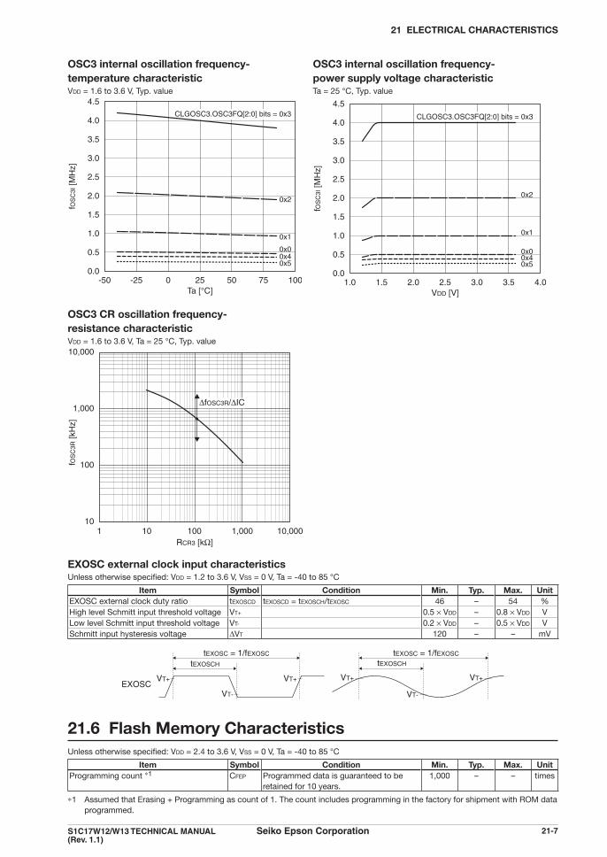
21 ELECTRICAL CHARACTERISTICS
S1C17W12/W13 TECHNICAL MANUAL Seiko Epson Corporation 21-7(Rev. 1.1)
OSC3 internal oscillation frequency- OSC3 internal oscillation frequency-temperature characteristic power supply voltage characteristicVDD = 1.6 to 3.6 V, Typ. value Ta = 25 °C, Typ. value
-50
4.5
4.0
3.5
3.0
2.5
2.0
1.5
1.0
0.5
0.0-25 0 25 50 75 100
Ta [°C]
fOS
C3I
[MHz]
CLGOSC3.OSC3FQ[2:0] bits = 0x3
0x2
0x1
0x0 0x4 0x5
1.0
4.5
4.0
3.5
3.0
2.5
2.0
1.5
1.0
0.5
0.01.5 2.0 2.5 3.0 3.5 4.0
VDD [V]
fOS
C3I
[MHz]
CLGOSC3.OSC3FQ[2:0] bits = 0x3
0x2
0x1
0x00x40x5
OSC3 CR oscillation frequency-resistance characteristicVDD = 1.6 to 3.6 V, Ta = 25 °C, Typ. value
1
10,000
1,000
100
1010 100 1,000 10,000
RCR3 [kΩ]
fOS
C3R
[kH
z]
∆fOSC3R/∆IC
EXOSC external clock input characteristicsUnless otherwise specified: VDD = 1.2 to 3.6 V, VSS = 0 V, Ta = -40 to 85 °C
Item Symbol Condition Min. Typ. Max. UnitEXOSC external clock duty ratio tEXOSCD tEXOSCD = tEXOSCH/tEXOSC 46 – 54 %High level Schmitt input threshold voltage VT+ 0.5 × VDD – 0.8 × VDD VLow level Schmitt input threshold voltage VT- 0.2 × VDD – 0.5 × VDD VSchmitt input hysteresis voltage DVT 120 – – mV
EXOSC
tEXOSCH
tEXOSC = 1/fEXOSC
VT+VT+
VT-
tEXOSCH
tEXOSC = 1/fEXOSC
VT+VT+
VT-
21.6 Flash Memory CharacteristicsUnless otherwise specified: VDD = 2.4 to 3.6 V, VSS = 0 V, Ta = -40 to 85 °C
Item Symbol Condition Min. Typ. Max. UnitProgramming count *1 CFEP Programmed data is guaranteed to be
retained for 10 years.1,000 – – times
*1 Assumed that Erasing + Programming as count of 1. The count includes programming in the factory for shipment with ROM data programmed.

21 ELECTRICAL CHARACTERISTICS
21-8 Seiko Epson Corporation S1C17W12/W13 TECHNICAL MANUAL (Rev. 1.1)
21.7 Input/Output Port (PPORT) CharacteristicsUnless otherwise specified: VDD = 1.2 to 3.6 V, VSS = 0 V, Ta = -40 to 85 °C
Item Symbol Condition VDD Min. Typ. Max. UnitHigh level Schmitt input threshold voltage
VT+ P00–07, P10–17, P20–26, P40–43, PD0–D1, PD3–D4 0.5 × VDD – 0.8 × VDD V
Low level Schmitt input threshold voltage
VT- P00–07, P10–17, P20–26, P40–43, PD0–D1, PD3–D4 0.2 × VDD – 0.5 × VDD V
Schmitt input hysteresis voltage
DVT P00–07, P10–17, P20–26, P40–43, PD0–D1, PD3–D4 120 – – mV
High level output current IOH P00–07, P10–17, P20–26, P40–43, PD0–D4, VOH = 0.9 × VDD
1.2 to 1.6 V – – -0.2 mA1.6 to 3.6 V – – -0.5 mA
Low level output current 1 IOL1 P00–07, P10–17, P20–26, P40–43, PD0–D4, VOL = 0.1 × VDD
1.2 to 1.6 V 0.2 – – mA1.6 to 3.6 V 0.5 – – mA
Low level output current 2 IOL2 P30–31, VOL = 0.1 × VDD 1.2 to 1.6 V 2 – – mA1.6 to 3.6 V 5 – – mA
Leakage current ILEAK P00–07, P10–17, P20–26, P30–31, P40–43, PD0–D4 -150 – 150 nAInput pull-up resistance RINU P00–07, P10–17, P20–26, P40–43, PD0–D1, PD3–D4 100 200 500 kWInput pull-down resistance RIND P00–07, P10–17, P20–26, P40–43, PD0–D1, PD3–D4 100 200 500 kWPin capacitance CIN P00–07, P10–17, P20–26, P40–43, PD0–D1, PD3–D4 – – 15 pF
High level
Low levelVT+VT-0
Input voltage [V]
Inpu
t dat
a
VDD 4.0 V*
(∗ For over voltage tolerant fail-safe type port)
High-level output current characteristicTa = 85 °C, Max. value
0.00
-2
-4
-6
-8
-10
0.2 0.4 0.6 0.8 1.00.1 0.3 0.5 0.7 0.9VDD–VOH [V]
IOH [m
A]
VDD = 1.2 V
VDD = 1.6 V
VDD = 3.6 V

21 ELECTRICAL CHARACTERISTICS
S1C17W12/W13 TECHNICAL MANUAL Seiko Epson Corporation 21-9(Rev. 1.1)
Low-level output current characteristic 1 Low-level output current characteristic 2Ta = 85 °C, Min. value Ta = 85 °C, Min. value
0.0 0.1 0.2 0.3 0.4 0.5 0.6 0.7 0.8 0.9 1.0
10
8
6
4
2
0
IOL1
[mA
]
VOL [V]
VDD = 3.6 V
VDD = 1.6 V
VDD = 1.2 V
0.0 0.1 0.2 0.3 0.4 0.5 0.6
18
16
14
12
10
8
6
4
2
0
IOL2
[mA
]
VOL [V]
VDD = 1.6 V
VDD = 1.2 V
21.8 Supply Voltage Detector (SVD) CharacteristicsUnless otherwise specified: VDD = 1.2 to 3.6 V, VSS = 0 V, Ta = -40 to 85 °C
Item Symbol Condition Min. Typ. Max. UnitEXSVD pin input voltage range VEXSVD 0 – 3.6 VEXSVD input impedance REXSVD SVDCTL.SVDC[4:0] bits = 0x01 253 288 322 kW
SVDCTL.SVDC[4:0] bits = 0x02 265 300 335 kWSVDCTL.SVDC[4:0] bits = 0x03 275 312 349 kWSVDCTL.SVDC[4:0] bits = 0x04 285 324 363 kWSVDCTL.SVDC[4:0] bits = 0x05 296 336 376 kWSVDCTL.SVDC[4:0] bits = 0x06 306 348 390 kWSVDCTL.SVDC[4:0] bits = 0x07 316 360 403 kWSVDCTL.SVDC[4:0] bits = 0x08 327 372 417 kWSVDCTL.SVDC[4:0] bits = 0x09 339 384 428 kWSVDCTL.SVDC[4:0] bits = 0x0a 348 396 443 kWSVDCTL.SVDC[4:0] bits = 0x0b 358 407 457 kWSVDCTL.SVDC[4:0] bits = 0x0c 379 431 484 kWSVDCTL.SVDC[4:0] bits = 0x0d 399 455 512 kWSVDCTL.SVDC[4:0] bits = 0x0e 419 479 540 kWSVDCTL.SVDC[4:0] bits = 0x0f 441 503 566 kWSVDCTL.SVDC[4:0] bits = 0x10 461 527 594 kWSVDCTL.SVDC[4:0] bits = 0x11 485 551 617 kWSVDCTL.SVDC[4:0] bits = 0x12 503 575 647 kWSVDCTL.SVDC[4:0] bits = 0x13 523 599 676 kWSVDCTL.SVDC[4:0] bits = 0x14 546 623 700 kWSVDCTL.SVDC[4:0] bits = 0x15 567 647 728 kWSVDCTL.SVDC[4:0] bits = 0x16 588 671 754 kWSVDCTL.SVDC[4:0] bits = 0x17 607 695 783 kWSVDCTL.SVDC[4:0] bits = 0x18 630 719 809 kWSVDCTL.SVDC[4:0] bits = 0x19 653 743 833 kWSVDCTL.SVDC[4:0] bits = 0x1a 676 767 859 kWSVDCTL.SVDC[4:0] bits = 0x1b 705 791 878 kWSVDCTL.SVDC[4:0] bits = 0x1c 721 815 909 kWSVDCTL.SVDC[4:0] bits = 0x1d 734 839 945 kWSVDCTL.SVDC[4:0] bits = 0x1e 757 863 970 kW

21 ELECTRICAL CHARACTERISTICS
21-10 Seiko Epson Corporation S1C17W12/W13 TECHNICAL MANUAL (Rev. 1.1)
Item Symbol Condition Min. Typ. Max. UnitSVD detection voltage VSVD SVDCTL.SVDC[4:0] bits = 0x01 1.17 1.20 1.23 V
SVDCTL.SVDC[4:0] bits = 0x02 1.22 1.25 1.28 VSVDCTL.SVDC[4:0] bits = 0x03 1.27 1.30 1.33 VSVDCTL.SVDC[4:0] bits = 0x04 1.32 1.35 1.38 VSVDCTL.SVDC[4:0] bits = 0x05 1.37 1.40 1.44 VSVDCTL.SVDC[4:0] bits = 0x06 1.41 1.45 1.49 VSVDCTL.SVDC[4:0] bits = 0x07 1.46 1.50 1.54 VSVDCTL.SVDC[4:0] bits = 0x08 1.51 1.55 1.59 VSVDCTL.SVDC[4:0] bits = 0x09 1.56 1.60 1.64 VSVDCTL.SVDC[4:0] bits = 0x0a 1.61 1.65 1.69 VSVDCTL.SVDC[4:0] bits = 0x0b 1.66 1.70 1.74 VSVDCTL.SVDC[4:0] bits = 0x0c 1.76 1.80 1.85 VSVDCTL.SVDC[4:0] bits = 0x0d 1.85 1.90 1.95 VSVDCTL.SVDC[4:0] bits = 0x0e 1.95 2.00 2.05 VSVDCTL.SVDC[4:0] bits = 0x0f 2.05 2.10 2.15 VSVDCTL.SVDC[4:0] bits = 0x10 2.15 2.20 2.26 VSVDCTL.SVDC[4:0] bits = 0x11 2.24 2.30 2.36 VSVDCTL.SVDC[4:0] bits = 0x12 2.34 2.40 2.46 VSVDCTL.SVDC[4:0] bits = 0x13 2.44 2.50 2.56 VSVDCTL.SVDC[4:0] bits = 0x14 2.54 2.60 2.67 VSVDCTL.SVDC[4:0] bits = 0x15 2.63 2.70 2.77 VSVDCTL.SVDC[4:0] bits = 0x16 2.73 2.80 2.87 VSVDCTL.SVDC[4:0] bits = 0x17 2.83 2.90 2.97 VSVDCTL.SVDC[4:0] bits = 0x18 2.93 3.00 3.08 VSVDCTL.SVDC[4:0] bits = 0x19 3.02 3.10 3.18 VSVDCTL.SVDC[4:0] bits = 0x1a 3.12 3.20 3.28 VSVDCTL.SVDC[4:0] bits = 0x1b 3.22 3.30 3.38 VSVDCTL.SVDC[4:0] bits = 0x1c 3.32 3.40 3.49 VSVDCTL.SVDC[4:0] bits = 0x1d 3.41 3.50 3.59 VSVDCTL.SVDC[4:0] bits = 0x1e 3.51 3.60 3.69 V
SVD circuit enable response time tSVDEN *1 – – 500 µsSVD circuit response time tSVD – – 60 µsSVD circuit current ISVD SVDCTL.SVDMD[1:0] bits = 0x0,
SVDCTL.SVDC[4:0] bits = 0x01, CLK_SVD = 32 kHz, Ta = 25 °C
– 18 31 µA
SVDCTL.SVDMD[1:0] bits = 0x1, SVDCTL.SVDC[4:0] bits = 0x01, CLK_SVD = 32 kHz, Ta = 25 °C
– 3.2 5.3 µA
SVDCTL.SVDMD[1:0] bits = 0x2, SVDCTL.SVDC[4:0] bits = 0x01, CLK_SVD = 32 kHz, Ta = 25 °C
– 1.7 2.8 µA
SVDCTL.SVDMD[1:0] bits = 0x3, SVDCTL.SVDC[4:0] bits = 0x01, CLK_SVD = 32 kHz, Ta = 25 °C
– 0.9 1.5 µA
*1 If CLK_SVD is configured in the neighborhood of 32 kHz, the SVDINTF.SVDDT bit is masked during the tSVDEN period and it re-tains the previous value.
CLK_SVD
SVDCTL.MODEN
SVDCTL.SVDC[4:0]
SVDINTF.SVDDT
tSVDtSVDEN
Invalid Valid ValidInvalid
0x1e 0x10

21 ELECTRICAL CHARACTERISTICS
S1C17W12/W13 TECHNICAL MANUAL Seiko Epson Corporation 21-11(Rev. 1.1)
SVD circuit current - power supply voltage characteristicTa = 25 °C, SVDCTL.SVDC[4:0] bits = 0x01, CLK_SVD = 32 kHz, Typ. value
1.0 1.5 2.0 2.5 3.0 3.5 4.0
20
18
16
14
12
10
8
6
4
2
0
VDD [V]
ISV
D [µ
A]
0x0
0x1
0x20x3
SVDCTL.SVDMD[1:0] bits =
21.9 UART (UART2) CharacteristicsUnless otherwise specified: VDD = 1.2 to 3.6 V, VSS = 0 V, Ta = -40 to 85 °C
Item Symbol Condition VDD Min. Typ. Max. UnitTransfer baud rate UBRT1 Normal mode 1.6 to 3.6 V 150 – 460,800 bps
1.2 to 1.6 V 150 – 57,600 bpsUBRT2 IrDA mode 1.6 to 3.6 V 150 – 115,200 bps
1.2 to 1.6 V 150 – 57,600 bps
21.10 Synchronous Serial Interface (SPIA) CharacteristicsUnless otherwise specified: VDD = 1.2 to 3.6 V, VSS = 0 V, Ta = -40 to 85 °C
Item Symbol Condition VDD Min. Typ. Max. UnitSPICLKn cycle time tSCYC 1.6 to 3.6 V 500 – – ns
1.2 to 1.6 V 1,000 – – nsSPICLKn High pulse width tSCKH 1.6 to 3.6 V 200 – – ns
1.2 to 1.6 V 400 – – nsSPICLKn Low pulse width tSCKL 1.6 to 3.6 V 200 – – ns
1.2 to 1.6 V 400 – – nsSDIn setup time tSDS 1.6 to 3.6 V 125 – – ns
1.2 to 1.6 V 250 – – nsSDIn hold time tSDH 1.6 to 3.6 V 70 – – ns
1.2 to 1.6 V 140 – – nsSDOn output delay time tSDO CL = 30 pF *1 1.6 to 3.6 V – – 120 ns
1.2 to 1.6 V – – 320 ns#SPISSn setup time tSSS 1.6 to 3.6 V 125 – – ns
1.2 to 1.6 V 250 – – ns#SPISSn High pulse width tSSH 1.6 to 3.6 V 80 – – ns
1.2 to 1.6 V 160 – – nsSDOn output start time tSDD CL = 30 pF *1 1.6 to 3.6 V – – 120 ns
1.2 to 1.6 V – – 320 nsSDOn output stop time tSDZ CL = 30 pF *1 1.6 to 3.6 V – – 80 ns
1.2 to 1.6 V – – 160 ns*1 CL = Pin load

21 ELECTRICAL CHARACTERISTICS
21-12 Seiko Epson Corporation S1C17W12/W13 TECHNICAL MANUAL (Rev. 1.1)
Master and slave modes
SPICLKn(CPOL, CPHA) = (1, 0) or (0, 1)
SPICLKn(CPOL, CPHA) = (1, 1) or (0, 0)
SDIn
SDOn
tSCYC
tSDO
tSCKH
tSDS tSDH
tSCKL
Slave mode
#SPISSn
SPICLKn(CPOL, CPHA) = (0, 1)
SPICLKn(CPOL, CPHA) = (1, 0)
SDIn
SDOn
tSDD
Hi-Z
tSSH
tSDZ
tSSS
21.11 I2C (I2C) CharacteristicsUnless otherwise specified: VDD = 1.2 to 3.6 V, VSS = 0 V, Ta = -40 to 85 °C
Item Symbol ConditionStandard mode
VDD = 1.2 to 3.6 VFast mode
VDD = 1.6 to 3.6 V UnitMin. Typ. Max. Min. Typ. Max.
SCLn frequency fSCL 0 – 100 0 – 400 kHzHold time (repeated) START condition *
tHD:STA 4.0 – – 0.6 – – µs
SCLn Low pulse width tLOW 4.7 – – 1.3 – – µsSCLn High pulse width tHIGH 4.0 – – 0.6 – – µsRepeated START condition setup time
tSU:STA 4.7 – – 0.6 – – µs
Data hold time tHD:DAT 0 – – 0 – – µsData setup time tSU:DAT 250 – – 100 – – nsSDAn, SCLn rise time tr – – 1,000 – – 300 nsSDAn, SCLn fall time tf – – 300 – – 300 nsSTOP condition setup time tSU:STO 4.0 – – 0.6 – – µsBus free time tBUF 4.7 – – 1.3 – – µs
* After this period, the first clock pulse is generated.
SDAn
SCLn S
tf tBUF
tHD:STA
1/fSCL
1st clock cycle
tf
9th clock cycle
S: START conditionSr: Repeated START conditionP: STOP condition
trtHD:DAT
tHIGH
tSU:STA
tLOW
tr tSU:DAT
Sr P S
tHD:STA
tSU:STO

21 ELECTRICAL CHARACTERISTICS
S1C17W12/W13 TECHNICAL MANUAL Seiko Epson Corporation 21-13(Rev. 1.1)
21.12 LCD Driver (LCD4A) CharacteristicsThe LCD driver characteristics varies depending on the panel load (panel size, drive duty, number of display pixels and display contents), so evaluate them by connecting to the actually used LCD panel. Unless otherwise specified: VDD = 1.2 to 3.6 V, VSS = 0 V, Ta = 25 °C, LCD4TIM2.BSTC[1:0] bits = 0x1 (Voltage booster clock = 2 kHz), No panel load
Item Symbol Condition Min. Typ. Max. UnitLCD drive voltage(VC2 reference voltage)VDD = 2.7 to 3.6 VLCD4PWR.VCSEL bit = 1
VC1 Connect 1 MW load resistor between VSS and VC1 0.32 × VC3 (Typ.)
– 0.35 × VC3 (Typ.)
V
VC2 Connect 1 MW load resistor between VSS and VC2 0.65 × VC3 (Typ.)
– 0.69 × VC3 (Typ.)
V
VC3 Connect 1 MW load resistor between VSS and VC3
LCD4PWR.LC[3:0] bits = 0x0 2.50 2.58 2.66 VLCD4PWR.LC[3:0] bits = 0x1 2.56 2.64 2.72 VLCD4PWR.LC[3:0] bits = 0x2 2.62 2.70 2.78 VLCD4PWR.LC[3:0] bits = 0x3 2.68 2.76 2.84 VLCD4PWR.LC[3:0] bits = 0x4 2.74 2.82 2.90 VLCD4PWR.LC[3:0] bits = 0x5 2.79 2.88 2.97 VLCD4PWR.LC[3:0] bits = 0x6 2.85 2.94 3.03 VLCD4PWR.LC[3:0] bits = 0x7 2.91 3.00 3.09 VLCD4PWR.LC[3:0] bits = 0x8 2.97 3.06 3.15 VLCD4PWR.LC[3:0] bits = 0x9 3.03 3.12 3.21 VLCD4PWR.LC[3:0] bits = 0xa 3.08 3.18 3.28 VLCD4PWR.LC[3:0] bits = 0xb 3.14 3.24 3.34 VLCD4PWR.LC[3:0] bits = 0xc 3.20 3.30 3.40 VLCD4PWR.LC[3:0] bits = 0xd 3.26 3.36 3.46 VLCD4PWR.LC[3:0] bits = 0xe 3.32 3.42 3.52 VLCD4PWR.LC[3:0] bits = 0xf 3.38 3.48 3.58 V
LCD drive voltage(VC1 reference voltage)VDD = 1.2 to 3.6 V *3
LCD4PWR.VCSEL bit = 0
VC1 Connect 1 MW load resistor between VSS and VC1 0.32 × VC3 (Typ.)
– 0.35 × VC3 (Typ.)
V
VC2 Connect 1 MW load resistor between VSS and VC2 0.65 × VC3 (Typ.)
– 0.69 × VC3 (Typ.)
V
VC3 Connect 1 MW load resistor between VSS and VC3
LCD4PWR.LC[3:0] bits = 0x0 2.49 2.57 2.65 VLCD4PWR.LC[3:0] bits = 0x1 2.55 2.63 2.71 VLCD4PWR.LC[3:0] bits = 0x2 2.61 2.69 2.77 VLCD4PWR.LC[3:0] bits = 0x3 2.67 2.75 2.83 VLCD4PWR.LC[3:0] bits = 0x4 2.73 2.81 2.89 VLCD4PWR.LC[3:0] bits = 0x5 2.78 2.87 2.96 VLCD4PWR.LC[3:0] bits = 0x6 2.84 2.93 3.02 VLCD4PWR.LC[3:0] bits = 0x7 2.90 2.99 3.08 VLCD4PWR.LC[3:0] bits = 0x8 2.96 3.05 3.14 VLCD4PWR.LC[3:0] bits = 0x9 3.02 3.11 3.20 VLCD4PWR.LC[3:0] bits = 0xa 3.07 3.17 3.27 VLCD4PWR.LC[3:0] bits = 0xb 3.13 3.23 3.33 VLCD4PWR.LC[3:0] bits = 0xc 3.19 3.29 3.39 VLCD4PWR.LC[3:0] bits = 0xd 3.25 3.35 3.45 VLCD4PWR.LC[3:0] bits = 0xe 3.31 3.41 3.51 VLCD4PWR.LC[3:0] bits = 0xf 3.37 3.47 3.57 V
Segment/Common output current
ISEGH SEGxx, COMyVSEGH = VC3/VC2/VC1 - 0.1 V, Ta = -40 to 85 °C
– – -10 µA
ISEGL SEGxx, COMyVSEGL = VSS/VC2/VC1 + 0.1 V, Ta = -40 to 85 °C
10 – – µA
LCD circuit current(VC2 reference voltage)
ILCD2 LCD4DSP.DSPC[1:0] bits = 0x1 (checker pattern), LCD4PWR.VCSEL bit = 1 *1 *2
– 1.5 3.0 µA
LCD4DSP.DSPC[1:0] bits = 0x2 (all on), LCD4PWR.VCSEL bit = 1 *1 *2
– 0.6 1.5 µA
LCD circuit current(VC1 reference voltage)
ILCD1 LCD4DSP.DSPC[1:0] bits = 0x1 (checker pattern), LCD4PWR.VCSEL bit = 0 *1 *2
– 2.7 6.0 µA
LCD4DSP.DSPC[1:0] bits = 0x2 (all on), LCD4PWR.VCSEL bit = 0 *1 *2
– 1.0 2.8 µA
LCD circuit currentin heavy load protection mode (VC2 reference voltage)
ILCD2H LCD4DSP.DSPC[1:0] bits = 0x2 (all on), LCD4PWR.VCSEL bit = 1,LCD4PWR.HVLD bit = 1 *1 *2
– 11 25 µA
LCD circuit currentin heavy load protection mode (VC1 reference voltage)
ILCD1H LCD4DSP.DSPC[1:0] bits = 0x2 (all on), LCD4PWR.VCSEL bit = 0,LCD4PWR.HVLD bit = 1 *1 *2
– 6 15 µA
*1 Other LCD driver settings: LCD4PWR.LC[3:0] bits = 0x1f, CLK_LCD4A = 32 kHz, LCD4TIM1.FRMCNT[3:0] bits = 0x7 (frame fre-quency = 64 Hz)
*2 The value is added to the current consumption in HALT/RUN mode. Current consumption increases according to the display contents and panel load.
*3 The LCD drive voltage is lower than the LCD4PWR.LC[3:0] bit settings when VDD = 1.2 to 1.6 V. See the LCD drive voltage-supply voltage characteristic graph shown below.
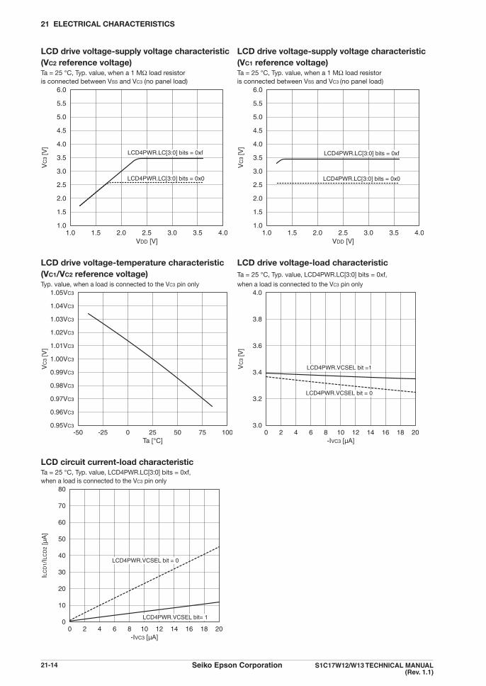
21 ELECTRICAL CHARACTERISTICS
21-14 Seiko Epson Corporation S1C17W12/W13 TECHNICAL MANUAL (Rev. 1.1)
LCD drive voltage-supply voltage characteristic LCD drive voltage-supply voltage characteristic(VC2 reference voltage) (VC1 reference voltage)Ta = 25 °C, Typ. value, when a 1 MW load resistor Ta = 25 °C, Typ. value, when a 1 MW load resistoris connected between VSS and VC3 (no panel load) is connected between VSS and VC3 (no panel load)
1.0 1.5 2.0 2.5 3.0 3.5 4.0
6.0
5.5
5.0
4.5
4.0
3.5
3.0
2.5
2.0
1.5
1.0
VDD [V]
VC
3 [V
]
LCD4PWR.LC[3:0] bits = 0xf
LCD4PWR.LC[3:0] bits = 0x0
1.0 1.5 2.0 2.5 3.0 3.5 4.0
6.0
5.5
5.0
4.5
4.0
3.5
3.0
2.5
2.0
1.5
1.0
VDD [V]V
C3
[V]
LCD4PWR.LC[3:0] bits = 0xf
LCD4PWR.LC[3:0] bits = 0x0
LCD drive voltage-temperature characteristic LCD drive voltage-load characteristic(VC1/VC2 reference voltage) Ta = 25 °C, Typ. value, LCD4PWR.LC[3:0] bits = 0xf, Typ. value, when a load is connected to the VC3 pin only when a load is connected to the VC3 pin only
-50
1.05VC3
1.04VC3
1.03VC3
1.02VC3
1.01VC3
1.00VC3
0.99VC3
0.98VC3
0.97VC3
0.96VC3
0.95VC3-25 0 25 50 75 100
Ta [°C]
VC
3 [V
]
0 2 4 6 8 10 12 14 16 18 20
4.0
3.8
3.6
3.4
3.2
3.0
-IVC3 [µA]
VC
3 [V
]
LCD4PWR.VCSEL bit = 0
LCD4PWR.VCSEL bit =1
LCD circuit current-load characteristicTa = 25 °C, Typ. value, LCD4PWR.LC[3:0] bits = 0xf, when a load is connected to the VC3 pin only
0 2 4 6 8 10 12 14 16 18 20
80
70
60
50
40
30
20
10
0
-IVC3 [µA]
ILC
D1/
ILC
D2
[µA]
LCD4PWR.VCSEL bit= 1
LCD4PWR.VCSEL bit = 0

21 ELECTRICAL CHARACTERISTICS
S1C17W12/W13 TECHNICAL MANUAL Seiko Epson Corporation 21-15(Rev. 1.1)
21.13 R/F Converter (RFC) CharacteristicsR/F converter characteristics change depending on conditions (board pattern, components used, etc.). Use these characteristic values as a reference and perform evaluation using the actual printed circuit board.
Unless otherwise specified: VDD = 1.2 to 3.6 V, VSS = 0 V, Ta = -40 to 85 °CItem Symbol Condition VDD Min. Typ. Max. Unit
Reference/sensor oscillation frequency fRFCLK 1 – 1,000 kHzReference/sensor oscillation frequency IC deviation
DfRFCLK/DIC Ta = 25 °C *1 1.6 to 3.6 V -40 – 40 %1.2 to 1.6 V -60 – 60 %
Reference resistor/resistive sensor resistance RREF, RSEN 10 – - kWReference capacitance CREF 100 – – pFTime base counter clock frequency fTCCLK 1.6 to 3.6 V – – 4.2 MHz
1.2 to 1.6 V – – 1.1 MHzHigh level Schmitt input threshold voltage VT+ 0.5 × VDD – 0.8 × VDD VLow level Schmitt input threshold voltage VT- 0.2 × VDD – 0.5 × VDD VSchmitt input hysteresis voltage DVT 120 – – mVR/F converter operating current(S1C17W12)
IRFC CREF = 1,000 pF, RREF/RSEN = 100 kW, Ta = 25 °C
3.6 V – 50 75 µA2.4 V – 25 38 µA2.0 V – 18 27 µA
R/F converter operating current(S1C17W13)
IRFC CREF = 1,000 pF, RREF/RSEN = 100 kW, Ta = 25 °C, VDD = 3.6 V
– 200 350 µA
*1 In this characteristic, unevenness between production lots, and variations in measurement board, resistances and capacitances are taken into account.
Waveforms for external clock input mode
RFINn
1/fRFCLK
VT+VT+
VT-
1/fRFCLK
VT+VT+
VT-
RFC reference/sensor oscillation frequency- RFC reference/sensor oscillation frequency-resistance characteristic capacitance characteristicCREF = 1,000 pF, Ta = 25 °C, Typ. value RREF/RSEN = 100 kW, Ta = 25 °C, Typ. value
1 10 100 1,000 10,000
10,000
1,000
100
10
1
0
RREF/RSEN [kΩ]
fRF
CLK
[kH
z]
VDD3.6 V1.6 V1.2 V
∆fRFCLK/∆IC
10
1,000
100
10
1
0100 1,000 10,000 100,000
CREF [pF]
fRF
CLK
[kH
z]
VDD3.6 V1.6 V1.2 V
∆fRFCLK/∆IC

21 ELECTRICAL CHARACTERISTICS
21-16 Seiko Epson Corporation S1C17W12/W13 TECHNICAL MANUAL (Rev. 1.1)
RFC reference/sensor oscillation frequency- RFC reference/sensor oscillation current temperature characteristic consumption-power supply voltage characteristicRREF/RSEN = 100 kW, CREF = 1,000 pF, Typ. value RREF/RSEN = 100 kW, CREF = 1,000 pF, Typ. value
-50
20
18
16
14
12
10
8
6
4
2
0-25 0 25 50 75 100
Ta [°C]
fRF
CLK
[kH
z]
VDD = 3.6 V
1.6 V1.2 V
1
250
200
150
100
50
01.5 2 2.5 3 3.5 4
VDD [V]IR
FC [µ
A]
S1C17W13
S1C17W12
RFC reference/sensor oscillation current RFC reference/sensor oscillation current consumption-frequency characteristic consumption-frequency characteristic(S1C17W12) (S1C17W13)CREF = 1,000 pF, Ta = 25 °C, Typ. value CREF = 1,000 pF, Ta = 25 °C, Typ. value
1 10 100 1,000
1,400
1,200
1,000
800
600
400
200
0
fRFCLK [kHz]
IRF
C [µ
A]
1.6 V
1.2 V
VDD = 3.6 V
1 10 100 1,000
1,400
1,200
1,000
800
600
400
200
0
fRFCLK [kHz]
IRF
C [µ
A]
1.6 V
1.2 V
VDD = 3.6 V

22 BASIC EXTERNAL CONNECTION DIAGRAM
S1C17W12/W13 TECHNICAL MANUAL Seiko Epson Corporation 22-1(Rev. 1.1)
22 Basic External Connection Diagram
CO
M0
CO
M3
SE
G0
SE
G25
BZOUT
EXSVD
Pxy
SDI0SDO0
SPICLK0#SPISS0
SCL0SDA0
USINnUSOUTn
TOUTn0/CAPn0TOUTn1/CAPn1
SENB0SENA0
REF0RFIN0
DCLK
DSIODST2
VPP
VDD
VD1
VD2
CV1
CV2
VC1
VC2
VC3
CP1
CP2
OSC1
OSC2
OSC3
OSC4
#RESET
VSS
RDBG
ICDmini
I/O
SPI
I2C
UART
PWM/Capture
VDD
VDD
CPW2
CPW3
CCV
CLCD1
CLCD2
CLCD3
CLCD4
RCR3
LCD panel26SEG × 4COM
CPW1+
S1C17W12/W13[The potential of the substrate
(back of the chip) is VSS.]
CD1
CG1( )
( )X'tal1
CD3
CG3
( )
( )
X'tal3/Ceramic
RTMP2
RTMP1
RREF
CREF
1.2–3.6 V, 2.4–3.6 V ∗1,or 2.5–3.6 V ∗2
∗5
( )∗3
∗4
∗6, ∗7, ∗8
∗6, ∗7, ∗8
∗6, ∗7, ∗8∗6, ∗7, ∗8∗6, ∗7, ∗8
∗8∗8∗8∗8
∗8
BZ
VDD
CVPP
REMO
VDD
IR transmitter module∗8∗8
∗6, ∗7
∗6, ∗7
∗6
∗6
*1: For Flash programming*2: For super economy mode*3: When OSC1 crystal oscillator is selected*4: When OSC3 CR oscillator is selected*5: When OSC3 crystal/ceramic oscillator is selected*6: The following pins are not available in the S1C17W12 SQFN7-48pin package. VD2, CV1, CV2, OSC1, OSC2, OSC3, OSC4, SEG0–SEG1, SEG20–SEG25 (18SEG × 4COM)*7: The following pins are not available in the S1C17W13 SQFN7-48pin package. VD2, CV1, CV2, OSC3, OSC4, SEG0–SEG1, SEG20–SEG25 (18SEG × 4COM)*8: The following pins are not available in the S1C17W13 TQFP12-48pin package. VD2, CV1, CV2, CP1, CP2, EXSVD, SENB0, SENA0, REF0, REFIN0, SEG20–SEG25 (20SEG × 4COM)( ): Do not mount components if unnecessary.

22 BASIC EXTERNAL CONNECTION DIAGRAM
22-2 Seiko Epson Corporation S1C17W12/W13 TECHNICAL MANUAL (Rev. 1.1)
Sample external componentsSymbol Name Recommended components
X'tal1 32 kHz crystal resonator C-002RX (R1 = 50 kW (Max.), CL = 7 pF) manufactured by Seiko Epson CorporationCG1 OSC1 gate capacitor Trimmer capacitor or ceramic capacitorCD1 OSC1 drain capacitor Ceramic capacitorX’tal3 Crystal resonator CA-301 (4 MHz) manufactured by Seiko Epson CorporationCeramic Ceramic resonator CSBLA_J (1 MHz) manufactured by Murata Manufacturing Co., Ltd.CG3 OSC3 gate capacitor Ceramic capacitorCD3 OSC3 drain capacitor Ceramic capacitorRCR3 OSC3 oscillating resistor Thick film chip resistorCPW1 Bypass capacitor between VSS and VDD Ceramic capacitor or electrolytic capacitor CPW2–3 Capacitors between VSS and VD1–2 Ceramic capacitorCCV Capacitor between CV1 and CV2 Ceramic capacitorCLCD1–3 Capacitors between VSS and VC1–3 Ceramic capacitorCLCD4 Capacitor between CP1 and CP2 Ceramic capacitorBZ Piezoelectric buzzer PS1240P02 manufactured by TDK CorporationRDBG DSIO pull-up resistor Thick film chip resistorRREF RFC reference resistor Thick film chip resistorRTMP1, 2 Resistive sensors Temperature sensor 103AP-2 manufactured by SEMITEC Corporation
Humidity sensor C15-M53R manufactured by SHINYEI Technology Co.,Ltd.(* In AC oscillation mode for resistive sensor measurements)
CREF RFC reference capacitor Ceramic capacitorCVPP Capacitor between VSS and VPP Ceramic capacitor* For recommended component values, refer to “Recommended Operating Conditions” in the “Electrical Characteristics” chapter.

23 PACKAGE
S1C17W12/W13 TECHNICAL MANUAL Seiko Epson Corporation 23-1(Rev. 1.1)
23 PackageQFP13-64pin package
(Unit: mm)
10
12
3348
10 12
17
32
INDEX
0.13min/0.27max
161
64
49
1.4
0.1
1.7m
ax
1
0.3min/0.75max
0.09min/0.2max
0.5
0°min/10°max
Figure 23.1 QFP13-64pin Package Dimensions

23 PACKAGE
23-2 Seiko Epson Corporation S1C17W12/W13 TECHNICAL MANUAL (Rev. 1.1)
SQFN7-48pin package(Unit: mm)
6.9min/7.1max
0.35min/0.45max
1
12
36
25
13 24
48 37
Index
6.9m
in/7
.1m
ax0m
in
1max
Top View
Bottom View
0.2m
in/0
.3m
ax
EXPOSED DIE PAD0.5
4.95min/5.15max
C0.3
4.95
min
/5.1
5max
Figure 23.2 SQFN7-48pin Package Dimensions
* The potential of the EXPOSED DIE PAD is the same as that of the substrate potential (VSS) on the back of the IC.

23 PACKAGE
S1C17W12/W13 TECHNICAL MANUAL Seiko Epson Corporation 23-3(Rev. 1.1)
TQFP12-48pin package(Unit: mm)
7
9
2536
7 9
13
24
INDEX
0.17min/0.27max
121
48
371
0.11.
2max
1
0.3min/0.7max
0°min/10°max
0.09min/0.2max
0.5
Figure 23.3 TQFP12-48pin Package Dimensions

APPENDIX A LIST OF PERIPHERAL CIRCUIT CONTROL REGISTERS
S1C17W12/W13 TECHNICAL MANUAL Seiko Epson Corporation AP-A-1(Rev. 1.1)
Appendix A List of Peripheral Circuit Control Registers
0x4000–0x4008 Misc Registers (MISC)
Address Register name Bit Bit name Initial Reset R/W Remarks
0x4000 MSCPROT (MISC System Protect Register)
15–0 PROT[15:0] 0x0000 H0 R/W –
0x4002 MSCIRAMSZ (MISC IRAM Size Register)
15–9 – 0x00 – R –8 (reserved) 0 H0 R/WP Always set to 0.
7–3 – 0x04 – R –2–0 IRAMSZ[2:0] 0x2 H0 R/WP
0x4004 MSCTTBRL(MISC Vector Table Address Low Register)
15–8 TTBR[15:8] 0x80 H0 R/WP –
7–0 TTBR[7:0] 0x00 H0 R
0x4006 MSCTTBRH(MISC Vector Table Address High Register)
15–8 – 0x00 – R –
7–0 TTBR[23:16] 0x00 H0 R/WP
0x4008 MSCPSR(MISC PSR Register)
15–8 – 0x00 – R –7–5 PSRIL[2:0] 0x0 H0 R4 PSRIE 0 H0 R3 PSRC 0 H0 R2 PSRV 0 H0 R1 PSRZ 0 H0 R0 PSRN 0 H0 R
0x4020–0x4026 Power Generator (PWG2)
Address Register name Bit Bit name Initial Reset R/W Remarks
0x4020 PWGCTL(PWG2 Control Register)
15–8 – 0x00 – R –7–3 – 0x00 – R2–0 PWGMOD[2:0] 0x0 H0 R/WP
0x4022 PWGTIM(PWG2 Timing Control Register)
15–8 – 0x00 – R –7–2 – 0x00 – R1–0 DCCCLK[1:0] 0x0 H0 R/WP
0x4024 PWGINTF(PWG2 Interrupt FlagRegister)
15–8 – 0x00 – R –7–1 – 0x00 – R0 MODCMPIF 0 H0 R/W
0x4026 PWGINTE(PWG2 Interrupt Enable Register)
15–8 – 0x00 – R –7–1 – 0x00 – R0 MODCMPIE 0 H0 R/W
0x4040–0x4052 Clock Generator (CLG)
Address Register name Bit Bit name Initial Reset R/W Remarks
0x4040 CLGSCLK(CLG System Clock Control Register)
15 WUPMD 0 H0 R/WP –14 – 0 – R
13–12 WUPDIV[1:0] 0x0 H0 R/WP11–10 – 0x0 – R9–8 WUPSRC[1:0] 0x0 H0 R/WP7–6 – 0x0 – R5–4 CLKDIV[1:0] 0x0 H0 R/WP3–2 – 0x0 – R1–0 CLKSRC[1:0] 0x0 H0 R/WP

APPENDIX A LIST OF PERIPHERAL CIRCUIT CONTROL REGISTERS
AP-A-2 Seiko Epson Corporation S1C17W12/W13 TECHNICAL MANUAL (Rev. 1.1)
Address Register name Bit Bit name Initial Reset R/W Remarks
0x4042 CLGOSC(CLG Oscillation Control Register)
15–12 – 0x0 – R –11 EXOSCSLPC 1 H0 R/W10 OSC3SLPC 1 H0 R/W9 OSC1SLPC 1 H0 R/W8 IOSCSLPC 1 H0 R/W
7–4 – 0x0 – R3 EXOSCEN 0 H0 R/W2 OSC3EN 0 H0 R/W1 OSC1EN 0 H0 R/W0 IOSCEN 1 H0 R/W
0x4044 CLGIOSC(CLG IOSC Control Register)
15–8 – 0x00 – R –7–5 – 0x0 – R4 IOSCSTM 0 H0 R/WP
3–0 – 0x0 – R0x4046 CLGOSC1
(CLG OSC1 Control Register)
15 – 0 – R –14 OSDRB 1 H0 R/WP13 OSDEN 0 H0 R/WP12 OSC1BUP 1 H0 R/WP11 OSC1SELCR 0 H0 R/WP
10–8 CGI1[2:0] 0x0 H0 R/WP7–6 INV1B[1:0] 0x2 H0 R/WP5–4 INV1N[1:0] 0x1 H0 R/WP3–2 – 0x0 – R1–0 OSC1WT[1:0] 0x2 H0 R/WP
0x4048 CLGOSC3(CLG OSC3 Control Register)
15–13 – 0x0 – R –12–10 OSC3FQ[2:0] 0x3 H0 R/WP9–8 OSC3MD[1:0] 0x0 H0 R/WP7–6 – 0x0 – R5–4 OSC3INV[1:0] 0x1 H0 R/WP3 – 0 – R
2–0 OSC3WT[2:0] 0x6 H0 R/WP0x404c CLGINTF
(CLG Interrupt Flag Register)
15–8 – 0x00 – R –7 – 0x0 – R6 (reserved) 0 H0 R5 OSC1STPIF 0 H0 R/W Cleared by writing 1.4 IOSCTEDIF 0 H0 R/W3 – 0 – R –2 OSC3STAIF 0 H0 R/W Cleared by writing 1.1 OSC1STAIF 0 H0 R/W0 IOSCSTAIF 0 H0 R/W
0x404e CLGINTE(CLG Interrupt Enable Register)
15–8 – 0x00 – R –7 – 0 – R6 (reserved) 0 H0 R5 OSC1STPIE 0 H0 R/W4 IOSCTEDIE 0 H0 R/W3 – 0 – R2 OSC3STAIE 0 H0 R/W1 OSC1STAIE 0 H0 R/W0 IOSCSTAIE 0 H0 R/W
0x4050 CLGFOUT(CLG FOUT Control Register)
15–8 – 0x00 – R –7 – 0 – R
6–4 FOUTDIV[2:0] 0x0 H0 R/W3–2 FOUTSRC[1:0] 0x0 H0 R/W1 – 0 – R0 FOUTEN 0 H0 R/W

APPENDIX A LIST OF PERIPHERAL CIRCUIT CONTROL REGISTERS
S1C17W12/W13 TECHNICAL MANUAL Seiko Epson Corporation AP-A-3(Rev. 1.1)
Address Register name Bit Bit name Initial Reset R/W Remarks
0x4052 CLGTRIM 15–13 – 0x0 – R –12–8 OSC3AJ[4:0] * H0 R/WP * Determined by factory
adjustment.7–6 – 0x0 – R –5–0 IOSCAJ[5:0] * H0 R/WP * Determined by factory
adjustment.
0x4080–0x4090 Interrupt Controller (ITC)
Address Register name Bit Bit name Initial Reset R/W Remarks
0x4080 ITCLV0(ITC Interrupt Level Setup Register 0)
15–11 – 0x00 – R –10–8 ILV1[2:0] 0x0 H0 R/W Port interrupt (ILVPPORT)7–3 – 0x00 – R –2–0 ILV0[2:0] 0x0 H0 R/W Supply voltage detector
interrupt (ILVSVD)0x4082 ITCLV1
(ITC Interrupt Level Setup Register 1)
15–11 – 0x00 – R –10–8 ILV3[2:0] 0x0 H0 R/W Clock generator interrupt
(ILVCLG)7–3 – 0x00 – R –2–0 ILV2[2:0] 0x0 H0 R/W Power generator interrupt
(ILVPWG2)0x4084 ITCLV2
(ITC Interrupt Level Setup Register 2)
15–11 – 0x00 – R –10–8 ILV5[2:0] 0x0 H0 R/W 16-bit timer Ch.0 interrupt
(ILVT16_0)7–3 – 0x00 – R –2–0 ILV4[2:0] 0x0 H0 R/W Real-time clock interrupt
(ILVRTCA_0)0x4086 ITCLV3
(ITC Interrupt Level Setup Register 3)
15–11 – 0x00 – R –10–8 ILV7[2:0] 0x0 H0 R/W 16-bit timer Ch.1 interrupt
(ILVT16_1)7–3 – 0x00 – R –2–0 ILV6[2:0] 0x0 H0 R/W UART Ch.0 interrupt
(ILVUART2_0)0x4088 ITCLV4
(ITC Interrupt Level Setup Register 4)
15–11 – 0x00 – R –10–8 ILV9[2:0] 0x0 H0 R/W I2C Ch.0 interrupt (ILVI2C_0)7–3 – 0x00 – R –2–0 ILV8[2:0] 0x0 H0 R/W Synchronous serial interface
Ch.0 interrupt (ILVSPIA_0)0x408a ITCLV5
(ITC Interrupt Level Setup Register 5)
15–11 – 0x00 – R –10–8 ILV11[2:0] 0x0 H0 R/W 16-bit PWM timer Ch.1
interrupt (ILVT16B_1)7–3 – 0x00 – R –2–0 ILV10[2:0] 0x0 H0 R/W 16-bit PWM timer Ch.0
interrupt (ILVT16B_0)0x408c ITCLV6
(ITC Interrupt Level Setup Register 6)
15–11 – 0x00 – R –10–8 ILV13[2:0] 0x0 H0 R/W 16-bit timer Ch.2 interrupt
(ILVT16_2) 7–3 – 0x00 – R –2–0 ILV12[2:0] 0x0 H0 R/W UART Ch.1 interrupt
(ILVUART2_1) 0x408e ITCLV7
(ITC Interrupt Level Setup Register 7)
15–11 – 0x00 – R –10–8 ILV15[2:0] 0x0 H0 R/W LCD driver interrupt
(ILVLCD4A)7–3 – 0x00 – R –2–0 ILV14[2:0] 0x0 H0 R/W Sound generator interrupt
(ILVSNDA_0)

APPENDIX A LIST OF PERIPHERAL CIRCUIT CONTROL REGISTERS
AP-A-4 Seiko Epson Corporation S1C17W12/W13 TECHNICAL MANUAL (Rev. 1.1)
Address Register name Bit Bit name Initial Reset R/W Remarks
0x4090 ITCLV8(ITC Interrupt Level Setup Register 8)
15–11 – 0x00 – R –10–8 ILV17[2:0] 0x0 H0 R/W IR remote controller interrupt
(ILVREMC2_0)7–3 – 0x00 – R –2–0 ILV16[2:0] 0x0 H0 R/W R/F converter Ch.0 interrupt
(ILVRFC_0)
0x40a0–0x40a4 Watchdog Timer (WDT2)
Address Register name Bit Bit name Initial Reset R/W Remarks
0x40a0 WDTCLK(WDT2 Clock Control Register)
15–9 – 0x00 – R –8 DBRUN 0 H0 R/WP
7–6 – 0x0 – R5–4 CLKDIV[1:0] 0x0 H0 R/WP3–2 – 0x0 – R1–0 CLKSRC[1:0] 0x0 H0 R/WP
0x40a2 WDTCTL(WDT2 Control Register)
15–11 – 0x00 – R –10–9 MOD[1:0] 0x0 H0 R/WP
8 STATNMI 0 H0 R7–5 – 0x0 – R4 WDTCNTRST 0 H0 WP Always read as 0.
3–0 WDTRUN[3:0] 0xa H0 R/WP –0x40a4 WDTCMP
(WDT2 Counter Com-pare Match Register)
15–10 – 0x00 – R –
9–0 CMP[9:0] 0x3ff H0 R/WP
0x40c0–0x40d2 Real-time Clock (RTCA)
Address Register name Bit Bit name Initial Reset R/W Remarks
0x40c0 RTCCTL(RTC Control Register)
15 RTCTRMBSY 0 H0 R –14–8 RTCTRM[6:0] 0x00 H0 W Read as 0x00.
7 – 0 – R –6 RTCBSY 0 H0 R5 RTCHLD 0 H0 R/W Cleared by setting the
RTCCTL.RTCRST bit to 1.4 RTC24H 0 H0 R/W –3 – 0 – R2 RTCADJ 0 H0 R/W Cleared by setting the
RTCCTL.RTCRST bit to 1.1 RTCRST 0 H0 R/W –0 RTCRUN 0 H0 R/W
0x40c2 RTCALM1(RTC Second Alarm Register)
15 – 0 – R –14–12 RTCSHA[2:0] 0x0 H0 R/W11–8 RTCSLA[3:0] 0x0 H0 R/W7–0 – 0x00 – R
0x40c4 RTCALM2(RTC Hour/Minute Alarm Register)
15 – 0 – R –14 RTCAPA 0 H0 R/W
13–12 RTCHHA[1:0] 0x0 H0 R/W11–8 RTCHLA[3:0] 0x0 H0 R/W
7 – 0 – R6–4 RTCMIHA[2:0] 0x0 H0 R/W3–0 RTCMILA[3:0] 0x0 H0 R/W
0x40c6 RTCSWCTL(RTC Stopwatch Control Register)
15–12 BCD10[3:0] 0x0 H0 R –11–8 BCD100[3:0] 0x0 H0 R7–5 – 0x0 – R4 SWRST 0 H0 W Read as 0.
3–1 – 0x0 – R –0 SWRUN 0 H0 R/W

APPENDIX A LIST OF PERIPHERAL CIRCUIT CONTROL REGISTERS
S1C17W12/W13 TECHNICAL MANUAL Seiko Epson Corporation AP-A-5(Rev. 1.1)
Address Register name Bit Bit name Initial Reset R/W Remarks
0x40c8 RTCSEC(RTC Second/1Hz Register)
15 – 0 – R –14–12 RTCSH[2:0] 0x0 H0 R/W11–8 RTCSL[3:0] 0x0 H0 R/W
7 RTC1HZ 0 H0 R Cleared by setting theRTCCTL.RTCRST bit to 1.6 RTC2HZ 0 H0 R
5 RTC4HZ 0 H0 R4 RTC8HZ 0 H0 R3 RTC16HZ 0 H0 R2 RTC32HZ 0 H0 R1 RTC64HZ 0 H0 R0 RTC128HZ 0 H0 R
0x40ca RTCHUR(RTC Hour/Minute Register)
15 – 0 – R –14 RTCAP 0 H0 R/W
13–12 RTCHH[1:0] 0x1 H0 R/W11–8 RTCHL[3:0] 0x2 H0 R/W
7 – 0 – R6–4 RTCMIH[2:0] 0x0 H0 R/W3–0 RTCMIL[3:0] 0x0 H0 R/W
0x40cc RTCMON(RTC Month/Day Register)
15–13 – 0x0 – R –12 RTCMOH 0 H0 R/W
11–8 RTCMOL[3:0] 0x1 H0 R/W7–6 – 0x0 – R5–4 RTCDH[1:0] 0x0 H0 R/W3–0 RTCDL[3:0] 0x1 H0 R/W
0x40ce RTCYAR(RTC Year/Week Register)
15–11 – 0x00 – R –10–8 RTCWK[2:0] 0x0 H0 R/W7–4 RTCYH[3:0] 0x0 H0 R/W3–0 RTCYL[3:0] 0x0 H0 R/W
0x40d0 RTCINTF(RTC Interrupt Flag Register)
15 RTCTRMIF 0 H0 R/W Cleared by writing 1.14 SW1IF 0 H0 R/W13 SW10IF 0 H0 R/W12 SW100IF 0 H0 R/W
11–9 – 0x0 – R –8 ALARMIF 0 H0 R/W Cleared by writing 1.7 1DAYIF 0 H0 R/W6 1HURIF 0 H0 R/W5 1MINIF 0 H0 R/W4 1SECIF 0 H0 R/W3 1_2SECIF 0 H0 R/W2 1_4SECIF 0 H0 R/W1 1_8SECIF 0 H0 R/W0 1_32SECIF 0 H0 R/W
0x40d2 RTCINTE(RTC Interrupt Enable Register)
15 RTCTRMIE 0 H0 R/W –14 SW1IE 0 H0 R/W13 SW10IE 0 H0 R/W12 SW100IE 0 H0 R/W
11–9 – 0x0 – R8 ALARMIE 0 H0 R/W7 1DAYIE 0 H0 R/W6 1HURIE 0 H0 R/W5 1MINIE 0 H0 R/W4 1SECIE 0 H0 R/W3 1_2SECIE 0 H0 R/W2 1_4SECIE 0 H0 R/W1 1_8SECIE 0 H0 R/W0 1_32SECIE 0 H0 R/W

APPENDIX A LIST OF PERIPHERAL CIRCUIT CONTROL REGISTERS
AP-A-6 Seiko Epson Corporation S1C17W12/W13 TECHNICAL MANUAL (Rev. 1.1)
0x4100–0x4106 Supply Voltage Detector (SVD)
Address Register name Bit Bit name Initial Reset R/W Remarks
0x4100 SVDCLK(SVD Clock Control Register)
15–9 – 0x00 – R –8 DBRUN 1 H0 R/WP7 – 0 – R
6–4 CLKDIV[2:0] 0x0 H0 R/WP3–2 – 0x0 – R1–0 CLKSRC[1:0] 0x0 H0 R/WP
0x4102 SVDCTL(SVD Control Register)
15 VDSEL 0 H1 R/WP –14–13 SVDSC[1:0] 0x0 H0 R/WP Writing takes effect when
the SVDCTL.SVDMD[1:0] bits are not 0x0.
12–8 SVDC[4:0] 0x1e H1 R/WP –7–4 SVDRE[3:0] 0x0 H1 R/WP3 – 0 – R
2–1 SVDMD[1:0] 0x0 H0 R/WP0 MODEN 0 H1 R/WP
0x4104 SVDINTF(SVD Status and In-terrupt Flag Register)
15–9 – 0x00 – R –8 SVDDT x – R
7–1 – 0x00 – R0 SVDIF 0 H1 R/W Cleared by writing 1.
0x4106 SVDINTE(SVD Interrupt Enable Register)
15–8 – 0x00 – R –7–1 – 0x00 – R0 SVDIE 0 H0 R/W
0x4160–0x416c 16-bit Timer (T16) Ch.0
Address Register name Bit Bit name Initial Reset R/W Remarks
0x4160 T16_0CLK(T16 Ch.0 Clock Control Register)
15–9 – 0x00 – R –8 DBRUN 0 H0 R/W
7–4 CLKDIV[3:0] 0x0 H0 R/W3–2 – 0x0 – R1–0 CLKSRC[1:0] 0x0 H0 R/W
0x4162 T16_0MOD(T16 Ch.0 Mode Register)
15–8 – 0x00 – R –7–1 – 0x00 – R0 TRMD 0 H0 R/W
0x4164 T16_0CTL(T16 Ch.0 Control Register)
15–9 – 0x00 – R –8 PRUN 0 H0 R/W
7–2 – 0x00 – R1 PRESET 0 H0 R/W0 MODEN 0 H0 R/W
0x4166 T16_0TR(T16 Ch.0 Reload Data Register)
15–0 TR[15:0] 0xffff H0 R/W –
0x4168 T16_0TC(T16 Ch.0 Counter Data Register)
15–0 TC[15:0] 0xffff H0 R –
0x416a T16_0INTF(T16 Ch.0 Interrupt Flag Register)
15–8 – 0x00 – R –7–1 – 0x00 – R0 UFIF 0 H0 R/W Cleared by writing 1.
0x416c T16_0INTE(T16 Ch.0 Interrupt Enable Register)
15–8 – 0x00 – R –7–1 – 0x00 – R0 UFIE 0 H0 R/W

APPENDIX A LIST OF PERIPHERAL CIRCUIT CONTROL REGISTERS
S1C17W12/W13 TECHNICAL MANUAL Seiko Epson Corporation AP-A-7(Rev. 1.1)
0x41b0 Flash Controller (FLASHC)
Address Register name Bit Bit name Initial Reset R/W Remarks
0x41b0 FLASHCWAIT(FLASHC Flash Read Cycle Register)
15–9 – 0x00 – R –8 (reserved) 1 H0 R/WP Always set to 1.
7–2 – 0x00 – R –1–0 RDWAIT[1:0] 0x1 H0 R/WP
0x4200–0x42e2 I/O Ports (PPORT)
Address Register name Bit Bit name Initial Reset R/W Remarks
0x4200 P0DAT(P0 Port Data Register)
15–8 P0OUT[7:0] 0x00 H0 R/W –
7–0 P0IN[7:0] 0x00 H0 R
0x4202 P0IOEN(P0 Port Enable Register)
15–8 P0IEN[7:0] 0x00 H0 R/W –
7–0 P0OEN[7:0] 0x00 H0 R/W
0x4204 P0RCTL(P0 Port Pull-up/down Control Register)
15–8 P0PDPU[7:0] 0x00 H0 R/W –
7–0 P0REN[7:0] 0x00 H0 R/W
0x4206 P0INTF(P0 Port Interrupt Flag Register)
15–8 – 0x00 – R –
7–0 P0IF[7:0] 0x00 H0 R/W Cleared by writing 1.
0x4208 P0INTCTL(P0 Port Interrupt Control Register)
15–8 P0EDGE[7:0] 0x00 H0 R/W –
7–0 P0IE[7:0] 0x00 H0 R/W
0x420a P0CHATEN(P0 Port Chattering Filter Enable Register)
15–8 – 0x00 – R –
7–0 P0CHATEN[7:0] 0x00 H0 R/W
0x420c P0MODSEL(P0 Port Mode Select Register)
15–8 – 0x00 – R –
7–0 P0SEL[7:0] 0x00 H0 R/W
0x420e P0FNCSEL(P0 Port Function Select Register)
15–14 P07MUX[1:0] 0x0 H0 R/W –13–12 P06MUX[1:0] 0x0 H0 R/W11–10 P05MUX[1:0] 0x0 H0 R/W9–8 P04MUX[1:0] 0x0 H0 R/W7–6 P03MUX[1:0] 0x0 H0 R/W5–4 P02MUX[1:0] 0x0 H0 R/W3–2 P01MUX[1:0] 0x0 H0 R/W1–0 P00MUX[1:0] 0x0 H0 R/W
0x4210 P1DAT(P1 Port Data Register)
15–8 P1OUT[7:0] 0x00 H0 R/W –
7–0 P1IN[7:0] 0x00 H0 R
0x4212 P1IOEN(P1 Port Enable Register)
15–8 P1IEN[7:0] 0x00 H0 R/W –
7–0 P1OEN[7:0] 0x00 H0 R/W
0x4214 P1RCTL(P1 Port Pull-up/down Control Register)
15–8 P1PDPU[7:0] 0x00 H0 R/W –
7–0 P1REN[7:0] 0x00 H0 R/W
0x4216 P1INTF(P1 Port Interrupt Flag Register)
15–8 – 0x00 – R –
7–0 P1IF[7:0] 0x00 H0 R/W Cleared by writing 1.
0x4218 P1INTCTL(P1 Port Interrupt Control Register)
15–8 P1EDGE[7:0] 0x00 H0 R/W –
7–0 P1IE[7:0] 0x00 H0 R/W
0x421a P1CHATEN(P1 Port Chattering Filter Enable Register)
15–8 – 0x00 – R –
7–0 P1CHATEN[7:0] 0x00 H0 R/W

APPENDIX A LIST OF PERIPHERAL CIRCUIT CONTROL REGISTERS
AP-A-8 Seiko Epson Corporation S1C17W12/W13 TECHNICAL MANUAL (Rev. 1.1)
Address Register name Bit Bit name Initial Reset R/W Remarks
0x421c P1MODSEL(P1 Port Mode Select Register)
15–8 – 0x00 – R –
7–0 P1SEL[7:0] 0x00 H0 R/W
0x421e P1FNCSEL(P1 Port Function Select Register)
15–14 P17MUX[1:0] 0x0 H0 R/W –13–12 P16MUX[1:0] 0x0 H0 R/W11–10 P15MUX[1:0] 0x0 H0 R/W9–8 P14MUX[1:0] 0x0 H0 R/W7–6 P13MUX[1:0] 0x0 H0 R/W5–4 P12MUX[1:0] 0x0 H0 R/W3–2 P11MUX[1:0] 0x0 H0 R/W1–0 P10MUX[1:0] 0x0 H0 R/W
0x4220 P2DAT(P2 Port Data Register)
15 – 0 – R –14–8 P2OUT[6:0] 0x00 H0 R/W
7 – 0 – R6–0 P2IN[6:0] 0x00 H0 R
0x4222 P2IOEN(P2 Port Enable Register)
15 – 0 – R –14–8 P2IEN[6:0] 0x00 H0 R/W
7 – 0 – R6–0 P2OEN[6:0] 0x00 H0 R/W
0x4224 P2RCTL(P2 Port Pull-up/down Control Register)
15 – 0 – R –14–8 P2PDPU[6:0] 0x00 H0 R/W
7 – 0 – R6–0 P2REN[6:0] 0x00 H0 R/W
0x4226 P2INTF(P2 Port Interrupt Flag Register)
15–8 – 0x00 – R –7 – 0 – R
6–0 P2IF[6:0] 0x00 H0 R/W Cleared by writing 1.0x4228 P2INTCTL
(P2 Port Interrupt Control Register)
15 – 0 – R –14–8 P2EDGE[6:0] 0x00 H0 R/W
7 – 0 – R6–0 P2IE[6:0] 0x00 H0 R/W
0x422a P2CHATEN(P2 Port Chattering Filter Enable Register)
15–8 – 0x00 – R –7 – 0 – R
6–0 P2CHATEN[6:0] 0x00 H0 R/W
0x422c P2MODSEL(P2 Port Mode Select Register)
15–8 – 0x00 – R –7 – 0 – R
6–0 P2SEL[6:0] 0x00 H0 R/W0x422e P2FNCSEL
(P2 Port Function Select Register)
15–14 – 0x0 – R –13–12 P26MUX[1:0] 0x0 H0 R/W11–10 P25MUX[1:0] 0x0 H0 R/W9–8 P24MUX[1:0] 0x0 H0 R/W7–6 P23MUX[1:0] 0x0 H0 R/W5–4 P22MUX[1:0] 0x0 H0 R/W3–2 P21MUX[1:0] 0x0 H0 R/W1–0 P20MUX[1:0] 0x0 H0 R/W
0x4230 P3DAT(P3 Port Data Register)
15–10 – 0x00 – R –9–8 P3OUT[1:0] 0x0 H0 R/W7–0 – 0x00 – R
0x4232 P3IOEN(P3 Port Enable Register)
15–8 – 0x00 – R –7–2 – 0x00 – R1–0 P3OEN[1:0] 0x0 H0 R/W
0x423c P3MODSEL(P3 Port Mode Select Register)
15–8 – 0x00 – R –7–2 – 0x00 – R1–0 P3SEL[1:0] 0x0 H0 R/W

APPENDIX A LIST OF PERIPHERAL CIRCUIT CONTROL REGISTERS
S1C17W12/W13 TECHNICAL MANUAL Seiko Epson Corporation AP-A-9(Rev. 1.1)
Address Register name Bit Bit name Initial Reset R/W Remarks
0x423e P3FNCSEL(P3 Port Function Select Register)
15–8 – 0x00 – R –7–4 – 0x0 – R3–2 P31MUX[1:0] 0x0 H0 R/W1–0 P30MUX[1:0] 0x0 H0 R/W
0x4240 P4DAT(P4 Port Data Register)
15–12 – 0x0 – R –11–8 P4OUT[3:0] 0x0 H0 R/W7–4 – 0x0 – R3–0 P4IN[3:0] 0x0 H0 R
0x4242 P4IOEN(P4 Port Enable Register)
15–12 – 0x0 – R –11–8 P4IEN[3:0] 0x0 H0 R/W7–4 – 0x0 – R3–0 P4OEN[3:0] 0x0 H0 R/W
0x4244 P4RCTL(P4 Port Pull-up/down Control Register)
15–12 – 0x0 – R –11–8 P4PDPU[3:0] 0x0 H0 R/W7–4 – 0x0 – R3–0 P4REN[3:0] 0x0 H0 R/W
0x4246 P4INTF(P4 Port Interrupt Flag Register)
15–8 – 0x00 – R –7–4 – 0x0 – R3–0 P4IF[3:0] 0x0 H0 R/W Cleared by writing 1.
0x4248 P4INTCTL(P4 Port Interrupt Control Register)
15–12 – 0x0 – R –11–8 P4EDGE[3:0] 0x0 H0 R/W7–4 – 0x0 – R3–0 P4IE[3:0] 0x0 H0 R/W
0x424a P4CHATEN(P4 Port Chattering Filter Enable Register)
15–8 – 0x00 – R –7–4 – 0x0 – R3–0 P4CHATEN[3:0] 0x0 H0 R/W
0x424c P4MODSEL(P4 Port Mode Select Register)
15–8 – 0x00 – R –7–4 – 0x0 – R3–0 P4SEL[3:0] 0x0 H0 R/W
0x424e P4FNCSEL(P4 Port Function Select Register)
15–8 – 0x00 – R –7–6 P43MUX[1:0] 0x3 H0 R/W5–4 P42MUX[1:0] 0x3 H0 R/W3–2 P41MUX[1:0] 0x3 H0 R/W1–0 P40MUX[1:0] 0x3 H0 R/W
0x42d0 PDDAT(Pd Port Data Register)
15–13 – 0x00 – R –12–8 PDOUT[4:0] 0x0 H0 R/W7–5 – 0x0 – R4–3 PDIN[4:3] x H0 R2 – 0 – R
1–0 PDIN[1:0] x H0 R0x42d2 PDIOEN
(Pd Port Enable Register)
15–13 – 0x0 – R –12–11 PDIEN[4:3] 0x0 H0 R/W
10 (reserved) 0 H0 R/W9–8 PDIEN[1:0] 0x0 H0 R/W7–5 – 0x0 – R4–0 PDOEN[4:0] 0x00 H0 R/W

APPENDIX A LIST OF PERIPHERAL CIRCUIT CONTROL REGISTERS
AP-A-10 Seiko Epson Corporation S1C17W12/W13 TECHNICAL MANUAL (Rev. 1.1)
Address Register name Bit Bit name Initial Reset R/W Remarks
0x42d4 PDRCTL(Pd Port Pull-up/down Control Register)
15–13 – 0x00 – R –12–11 PDPDPU[4:3] 0x0 H0 R/W
10 (reserved) 0 H0 R/W9–8 PDPDPU[1:0] 0x0 H0 R/W7–5 – 0x00 – R4–3 PDREN[4:3] 0x0 H0 R/W2 (reserved) 0 H0 R/W
1–0 PDREN[1:0] 0x0 H0 R/W0x42dc PDMODSEL
(Pd Port Mode Select Register)
15–8 – 0x00 – R –7–5 – 0x0 – R4–0 PDSEL[4:0] 0x07 H0 R/W
0x42de PDFNCSEL(Pd Port Function Select Register)
15–10 – 0x00 – R –9–8 PD4MUX[1:0] 0x0 H0 R/W7–6 PD3MUX[1:0] 0x0 H0 R/W5–4 PD2MUX[1:0] 0x0 H0 R/W3–2 PD1MUX[1:0] 0x0 H0 R/W1–0 PD0MUX[1:0] 0x0 H0 R/W
0x42e0 PCLK(P Port Clock Control Register)
15–9 – 0x00 – R –8 DBRUN 0 H0 R/WP
7–4 CLKDIV[3:0] 0x0 H0 R/WP3–2 KRSTCFG[1:0] 0x0 H0 R/WP1–0 CLKSRC[1:0] 0x0 H0 R/WP
0x42e2 PINTFGRP(P Port Interrupt Flag Group Register)
15–8 – 0x00 – R –7–5 – 0x0 – R4 P4INT 0 H0 R3 – 0 – R2 P2INT 0 H0 R1 P1INT 0 H0 R0 P0INT 0 H0 R
0x4300–0x4316 Universal Port Multiplexer (UPMUX)
Address Register name Bit Bit name Initial Reset R/W Remarks
0x4300 P0UPMUX0(P00–01 Universal Port Multiplexer Setting Register)
15–13 P01PPFNC[2:0] 0x0 H0 R/W –12–11 P01PERICH[1:0] 0x0 H0 R/W10–8 P01PERISEL[2:0] 0x0 H0 R/W7–5 P00PPFNC[2:0] 0x0 H0 R/W4–3 P00PERICH[1:0] 0x0 H0 R/W2–0 P00PERISEL[2:0] 0x0 H0 R/W
0x4302 P0UPMUX1(P02–03 Universal Port Multiplexer Setting Register)
15–13 P03PPFNC[2:0] 0x0 H0 R/W –12–11 P03PERICH[1:0] 0x0 H0 R/W10–8 P03PERISEL[2:0] 0x0 H0 R/W7–5 P02PPFNC[2:0] 0x0 H0 R/W4–3 P02PERICH[1:0] 0x0 H0 R/W2–0 P02PERISEL[2:0] 0x0 H0 R/W
0x4304 P0UPMUX2(P04–05 Universal Port Multiplexer Setting Register)
15–13 P05PPFNC[2:0] 0x0 H0 R/W –12–11 P05PERICH[1:0] 0x0 H0 R/W10–8 P05PERISEL[2:0] 0x0 H0 R/W7–5 P04PPFNC[2:0] 0x0 H0 R/W4–3 P04PERICH[1:0] 0x0 H0 R/W2–0 P04PERISEL[2:0] 0x0 H0 R/W
0x4306 P0UPMUX3(P06–07 Universal Port Multiplexer Setting Register)
15–13 P07PPFNC[2:0] 0x0 H0 R/W –12–11 P07PERICH[1:0] 0x0 H0 R/W10–8 P07PERISEL[2:0] 0x0 H0 R/W7–5 P06PPFNC[2:0] 0x0 H0 R/W4–3 P06PERICH[1:0] 0x0 H0 R/W2–0 P06PERISEL[2:0] 0x0 H0 R/W

APPENDIX A LIST OF PERIPHERAL CIRCUIT CONTROL REGISTERS
S1C17W12/W13 TECHNICAL MANUAL Seiko Epson Corporation AP-A-11(Rev. 1.1)
Address Register name Bit Bit name Initial Reset R/W Remarks
0x4308 P1UPMUX0(P10–11 Universal Port Multiplexer Setting Register)
15–13 P11PPFNC[2:0] 0x0 H0 R/W –12–11 P11PERICH[1:0] 0x0 H0 R/W10–8 P11PERISEL[2:0] 0x0 H0 R/W7–5 P10PPFNC[2:0] 0x0 H0 R/W4–3 P10PERICH[1:0] 0x0 H0 R/W2–0 P10PERISEL[2:0] 0x0 H0 R/W
0x430a P1UPMUX1(P12–13 Universal Port Multiplexer Setting Register)
15–13 P13PPFNC[2:0] 0x0 H0 R/W –12–11 P13PERICH[1:0] 0x0 H0 R/W10–8 P13PERISEL[2:0] 0x0 H0 R/W7–5 P12PPFNC[2:0] 0x0 H0 R/W4–3 P12PERICH[1:0] 0x0 H0 R/W2–0 P12PERISEL[2:0] 0x0 H0 R/W
0x430c P1UPMUX2(P14–15 Universal Port Multiplexer Setting Register)
15–13 P15PPFNC[2:0] 0x0 H0 R/W –12–11 P15PERICH[1:0] 0x0 H0 R/W10–8 P15PERISEL[2:0] 0x0 H0 R/W7–5 P14PPFNC[2:0] 0x0 H0 R/W4–3 P14PERICH[1:0] 0x0 H0 R/W2–0 P14PERISEL[2:0] 0x0 H0 R/W
0x430e P1UPMUX3(P16–17 Universal Port Multiplexer Setting Register)
15–13 P17PPFNC[2:0] 0x0 H0 R/W –12–11 P17PERICH[1:0] 0x0 H0 R/W10–8 P17PERISEL[2:0] 0x0 H0 R/W7–5 P16PPFNC[2:0] 0x0 H0 R/W4–3 P16PERICH[1:0] 0x0 H0 R/W2–0 P16PERISEL[2:0] 0x0 H0 R/W
0x4310 P2UPMUX0(P20–21 Universal Port Multiplexer Setting Register)
15–13 P21PPFNC[2:0] 0x0 H0 R/W –12–11 P21PERICH[1:0] 0x0 H0 R/W10–8 P21PERISEL[2:0] 0x0 H0 R/W7–5 P20PPFNC[2:0] 0x0 H0 R/W4–3 P20PERICH[1:0] 0x0 H0 R/W2–0 P20PERISEL[2:0] 0x0 H0 R/W
0x4312 P2UPMUX1(P22–23 Universal Port Multiplexer Setting Register)
15–13 P23PPFNC[2:0] 0x0 H0 R/W –12–11 P23PERICH[1:0] 0x0 H0 R/W10–8 P23PERISEL[2:0] 0x0 H0 R/W7–5 P22PPFNC[2:0] 0x0 H0 R/W4–3 P22PERICH[1:0] 0x0 H0 R/W2–0 P22PERISEL[2:0] 0x0 H0 R/W
0x4314 P2UPMUX2(P24–25 Universal Port Multiplexer Setting Register)
15–13 P25PPFNC[2:0] 0x0 H0 R/W –12–11 P25PERICH[1:0] 0x0 H0 R/W10–8 P25PERISEL[2:0] 0x0 H0 R/W7–5 P24PPFNC[2:0] 0x0 H0 R/W4–3 P24PERICH[1:0] 0x0 H0 R/W2–0 P24PERISEL[2:0] 0x0 H0 R/W
0x4316 P2UPMUX3(P26–27 Universal Port Multiplexer Setting Register)
15–8 – 0x00 – R –7–5 P26PPFNC[2:0] 0x0 H0 R/W4–3 P26PERICH[1:0] 0x0 H0 R/W2–0 P26PERISEL[2:0] 0x0 H0 R/W
0x4380–0x438e UART (UART2) Ch.0
Address Register name Bit Bit name Initial Reset R/W Remarks
0x4380 UA0CLK(UART2 Ch.0 Clock Control Register)
15–9 – 0x00 – R –8 DBRUN 0 H0 R/W
7–6 – 0x0 – R5–4 CLKDIV[1:0] 0x0 H0 R/W3–2 – 0x0 – R1–0 CLKSRC[1:0] 0x0 H0 R/W

APPENDIX A LIST OF PERIPHERAL CIRCUIT CONTROL REGISTERS
AP-A-12 Seiko Epson Corporation S1C17W12/W13 TECHNICAL MANUAL (Rev. 1.1)
Address Register name Bit Bit name Initial Reset R/W Remarks
0x4382 UA0MOD(UART2 Ch.0 Mode Register)
15–11 – 0x00 – R –10 BRDIV 0 H0 R/W9 INVRX 0 H0 R/W8 INVTX 0 H0 R/W7 – 0 – R6 PUEN 0 H0 R/W5 OUTMD 0 H0 R/W4 IRMD 0 H0 R/W3 CHLN 0 H0 R/W2 PREN 0 H0 R/W1 PRMD 0 H0 R/W0 STPB 0 H0 R/W
0x4384 UA0BR(UART2 Ch.0 Baud-Rate Register)
15–12 – 0x0 – R –11–8 FMD[3:0] 0x0 H0 R/W7–0 BRT[7:0] 0x00 H0 R/W
0x4386 UA0CTL(UART2 Ch.0 Control Register)
15–8 – 0x00 – R –7–2 – 0x00 – R1 SFTRST 0 H0 R/W0 MODEN 0 H0 R/W
0x4388 UA0TXD(UART2 Ch.0 Trans-mit Data Register)
15–8 – 0x00 – R –
7–0 TXD[7:0] 0x00 H0 R/W
0x438a UA0RXD(UART2 Ch.0 Receive Data Register)
15–8 – 0x00 – R –
7–0 RXD[7:0] 0x00 H0 R
0x438c UA0INTF(UART2 Ch.0 Status and Interrupt Flag Register)
15–10 – 0x00 – R –9 RBSY 0 H0/S0 R8 TBSY 0 H0/S0 R7 – 0 – R6 TENDIF 0 H0/S0 R/W Cleared by writing 1.5 FEIF 0 H0/S0 R/W Cleared by writing 1 or read-
ing the UA0RXD register.4 PEIF 0 H0/S0 R/W3 OEIF 0 H0/S0 R/W Cleared by writing 1.2 RB2FIF 0 H0/S0 R Cleared by reading the
UA0RXD register.1 RB1FIF 0 H0/S0 R0 TBEIF 1 H0/S0 R Cleared by writing to the
UA0TXD register.0x438e UA0INTE
(UART2 Ch.0 Inter-rupt Enable Register)
15–8 – 0x00 – R –7 – 0 – R6 TENDIE 0 H0 R/W5 FEIE 0 H0 R/W4 PEIE 0 H0 R/W3 OEIE 0 H0 R/W2 RB2FIE 0 H0 R/W1 RB1FIE 0 H0 R/W0 TBEIE 0 H0 R/W
0x43a0–0x43ac 16-bit Timer (T16) Ch.1
Address Register name Bit Bit name Initial Reset R/W Remarks
0x43a0 T16_1CLK(T16 Ch.1 Clock Control Register)
15–9 – 0x00 – R –8 DBRUN 0 H0 R/W
7–4 CLKDIV[3:0] 0x0 H0 R/W3–2 – 0x0 – R1–0 CLKSRC[1:0] 0x0 H0 R/W
0x43a2 T16_1MOD(T16 Ch.1 Mode Register)
15–8 – 0x00 – R –7–1 – 0x00 – R0 TRMD 0 H0 R/W

APPENDIX A LIST OF PERIPHERAL CIRCUIT CONTROL REGISTERS
S1C17W12/W13 TECHNICAL MANUAL Seiko Epson Corporation AP-A-13(Rev. 1.1)
Address Register name Bit Bit name Initial Reset R/W Remarks
0x43a4 T16_1CTL(T16 Ch.1 Control Register)
15–9 – 0x00 – R –8 PRUN 0 H0 R/W
7–2 – 0x00 – R1 PRESET 0 H0 R/W0 MODEN 0 H0 R/W
0x43a6 T16_1TR(T16 Ch.1 Reload Data Register)
15–0 TR[15:0] 0xffff H0 R/W –
0x43a8 T16_1TC(T16 Ch.1 Counter Data Register)
15–0 TC[15:0] 0xffff H0 R –
0x43aa T16_1INTF(T16 Ch.1 Interrupt Flag Register)
15–8 – 0x00 – R –7–1 – 0x00 – R0 UFIF 0 H0 R/W Cleared by writing 1.
0x43ac T16_1INTE(T16 Ch.1 Interrupt Enable Register)
15–8 – 0x00 – R –7–1 – 0x00 – R0 UFIE 0 H0 R/W
0x43b0–0x43ba Synchronous Serial Interface (SPIA) Ch.0
Address Register name Bit Bit name Initial Reset R/W Remarks
0x43b0 SPI0MOD(SPIA Ch.0 Mode Register)
15–12 – 0x0 – R –11–8 CHLN[3:0] 0x7 H0 R/W7–6 – 0x0 – R5 PUEN 0 H0 R/W4 NOCLKDIV 0 H0 R/W3 LSBFST 0 H0 R/W2 CPHA 0 H0 R/W1 CPOL 0 H0 R/W0 MST 0 H0 R/W
0x43b2 SPI0CTL(SPIA Ch.0 Control Register)
15–8 – 0x00 – R –7–2 – 0x00 – R1 SFTRST 0 H0 R/W0 MODEN 0 H0 R/W
0x43b4 SPI0TXD(SPIA Ch.0 Transmit Data Register)
15–0 TXD[15:0] 0x0000 H0 R/W –
0x43b6 SPI0RXD(SPIA Ch.0 Receive Data Register)
15–0 RXD[15:0] 0x0000 H0 R –
0x43b8 SPI0INTF(SPIA Ch.0 Interrupt Flag Register)
15–8 – 0x00 – R –7 BSY 0 H0 R
6–4 – 0x0 – R3 OEIF 0 H0/S0 R/W Cleared by writing 1.2 TENDIF 0 H0/S0 R/W1 RBFIF 0 H0/S0 R Cleared by reading the
SPI0RXD register.0 TBEIF 1 H0/S0 R Cleared by writing to the
SPI0TXD register.0x43ba SPI0INTE
(SPIA Ch.0 Interrupt Enable Register)
15–8 – 0x00 – R –7–4 – 0x0 – R3 OEIE 0 H0 R/W2 TENDIE 0 H0 R/W1 RBFIE 0 H0 R/W0 TBEIE 0 H0 R/W

APPENDIX A LIST OF PERIPHERAL CIRCUIT CONTROL REGISTERS
AP-A-14 Seiko Epson Corporation S1C17W12/W13 TECHNICAL MANUAL (Rev. 1.1)
0x43c0–0x43d2 I2C (I2C) Ch.0
Address Register name Bit Bit name Initial Reset R/W Remarks
0x43c0 I2C0CLK(I2C Ch.0 Clock Control Register)
15–9 – 0x00 – R –8 DBRUN 0 H0 R/W
7–6 – 0x0 – R5–4 CLKDIV[1:0] 0x0 H0 R/W3–2 – 0x0 – R1–0 CLKSRC[1:0] 0x0 H0 R/W
0x43c2 I2C0MOD(I2C Ch.0 Mode Register)
15–8 – 0x00 – R –7–3 – 0x00 – R2 OADR10 0 H0 R/W1 GCEN 0 H0 R/W0 – 0 – R
0x43c4 I2C0BR(I2C Ch.0 Baud-Rate Register)
15–8 – 0x00 – R –7 – 0 – R
6–0 BRT[6:0] 0x7f H0 R/W0x43c8 I2C0OADR
(I2C Ch.0 Own Address Register)
15–10 – 0x00 – R –
9–0 OADR[9:0] 0x000 H0 R/W
0x43ca I2C0CTL(I2C Ch.0 Control Register)
15–8 – 0x00 – R –7–6 – 0x0 – R5 MST 0 H0 R/W4 TXNACK 0 H0/S0 R/W3 TXSTOP 0 H0/S0 R/W2 TXSTART 0 H0/S0 R/W1 SFTRST 0 H0 R/W0 MODEN 0 H0 R/W
0x43cc I2C0TXD(I2C Ch.0 Transmit Data Register)
15–8 – 0x00 – R –
7–0 TXD[7:0] 0x00 H0 R/W
0x43ce I2C0RXD(I2C Ch.0 Receive Data Register)
15–8 – 0x00 – R –
7–0 RXD[7:0] 0x00 H0 R
0x43d0 I2C0INTF(I2C Ch.0 Status and Interrupt Flag Register)
15–13 – 0x0 – R –12 SDALOW 0 H0 R11 SCLLOW 0 H0 R10 BSY 0 H0/S0 R9 TR 0 H0 R8 – 0 – R7 BYTEENDIF 0 H0/S0 R/W Cleared by writing 1.6 GCIF 0 H0/S0 R/W5 NACKIF 0 H0/S0 R/W4 STOPIF 0 H0/S0 R/W3 STARTIF 0 H0/S0 R/W2 ERRIF 0 H0/S0 R/W1 RBFIF 0 H0/S0 R Cleared by reading the
I2C0RXD register.0 TBEIF 0 H0/S0 R Cleared by writing to the
I2C0TXD register.0x43d2 I2C0INTE
(I2C Ch.0 Interrupt Enable Register)
15–8 – 0x00 – R –7 BYTEENDIE 0 H0 R/W6 GCIE 0 H0 R/W5 NACKIE 0 H0 R/W4 STOPIE 0 H0 R/W3 STARTIE 0 H0 R/W2 ERRIE 0 H0 R/W1 RBFIE 0 H0 R/W0 TBEIE 0 H0 R/W

APPENDIX A LIST OF PERIPHERAL CIRCUIT CONTROL REGISTERS
S1C17W12/W13 TECHNICAL MANUAL Seiko Epson Corporation AP-A-15(Rev. 1.1)
0x5000–0x501a 16-bit PWM Timer (T16B) Ch.0
Address Register name Bit Bit name Initial Reset R/W Remarks
0x5000 T16B0CLK(T16B Ch.0 Clock Control Register)
15–9 – 0x00 – R –8 DBRUN 0 H0 R/W
7–4 CLKDIV[3:0] 0x0 H0 R/W3 – 0 – R
2–0 CLKSRC[2:0] 0x0 H0 R/W0x5002 T16B0CTL
(T16B Ch.0 Counter Control Register)
15–9 – 0x00 – R –8 MAXBSY 0 H0 R
7–6 – 0x0 – R5–4 CNTMD[1:0] 0x0 H0 R/W3 ONEST 0 H0 R/W2 RUN 0 H0 R/W1 PRESET 0 H0 R/W0 MODEN 0 H0 R/W
0x5004 T16B0MC(T16B Ch.0 Max Counter Data Register)
15–0 MC[15:0] 0xffff H0 R/W –
0x5006 T16B0TC(T16B Ch.0 Timer Counter Data Register)
15–0 TC[15:0] 0x0000 H0 R –
0x5008 T16B0CS(T16B Ch.0 Counter Status Register)
15–8 – 0x00 – R –7–4 – 0x0 – R3 CAPI1 0 H0 R2 CAPI0 0 H0 R1 UP_DOWN 1 H0 R0 BSY 0 H0 R
0x500a T16B0INTF(T16B Ch.0 Interrupt Flag Register)
15–8 – 0x00 – R –7–6 – 0x0 – R5 CAPOW1IF 0 H0 R/W Cleared by writing 1.4 CMPCAP1IF 0 H0 R/W3 CAPOW0IF 0 H0 R/W2 CMPCAP0IF 0 H0 R/W1 CNTMAXIF 0 H0 R/W0 CNTZEROIF 0 H0 R/W
0x500c T16B0INTE(T16B Ch.0 Interrupt Enable Register)
15–8 – 0x00 – R –7–6 – 0x0 – R5 CAPOW1IE 0 H0 R/W4 CMPCAP1IE 0 H0 R/W3 CAPOW0IE 0 H0 R/W2 CMPCAP0IE 0 H0 R/W1 CNTMAXIE 0 H0 R/W0 CNTZEROIE 0 H0 R/W
0x5010 T16B0CCCTL0(T16B Ch.0 Compare/Capture 0 Control Register)
15 SCS 0 H0 R/W –14–12 CBUFMD[2:0] 0x0 H0 R/W11–10 CAPIS[1:0] 0x0 H0 R/W
9–8 CAPTRG[1:0] 0x0 H0 R/W7 – 0 – R6 TOUTMT 0 H0 R/W5 TOUTO 0 H0 R/W
4–2 TOUTMD[2:0] 0x0 H0 R/W1 TOUTINV 0 H0 R/W0 CCMD 0 H0 R/W
0x5012 T16B0CCR0(T16B Ch.0 Compare/Capture 0 Data Register)
15–0 CC[15:0] 0x0000 H0 R/W –

APPENDIX A LIST OF PERIPHERAL CIRCUIT CONTROL REGISTERS
AP-A-16 Seiko Epson Corporation S1C17W12/W13 TECHNICAL MANUAL (Rev. 1.1)
Address Register name Bit Bit name Initial Reset R/W Remarks
0x5018 T16B0CCCTL1(T16B Ch.0 Compare/Capture 1 Control Register)
15 SCS 0 H0 R/W –14–12 CBUFMD[2:0] 0x0 H0 R/W11–10 CAPIS[1:0] 0x0 H0 R/W
9–8 CAPTRG[1:0] 0x0 H0 R/W7 – 0 – R6 TOUTMT 0 H0 R/W5 TOUTO 0 H0 R/W
4–2 TOUTMD[2:0] 0x0 H0 R/W1 TOUTINV 0 H0 R/W0 CCMD 0 H0 R/W
0x501a T16B0CCR1(T16B Ch.0 Compare/Capture 1 Data Register)
15–0 CC[15:0] 0x0000 H0 R/W –
0x5040–0x505a 16-bit PWM Timer (T16B) Ch.1
Address Register name Bit Bit name Initial Reset R/W Remarks
0x5040 T16B1CLK(T16B Ch.1 Clock Control Register)
15–9 – 0x00 – R –8 DBRUN 0 H0 R/W
7–4 CLKDIV[3:0] 0x0 H0 R/W3 – 0 – R
2–0 CLKSRC[2:0] 0x0 H0 R/W0x5042 T16B1CTL
(T16B Ch.1 Counter Control Register)
15–9 – 0x00 – R –8 MAXBSY 0 H0 R
7–6 – 0x0 – R5–4 CNTMD[1:0] 0x0 H0 R/W3 ONEST 0 H0 R/W2 RUN 0 H0 R/W1 PRESET 0 H0 R/W0 MODEN 0 H0 R/W
0x5044 T16B1MC(T16B Ch.1 Max Counter Data Register)
15–0 MC[15:0] 0xffff H0 R/W –
0x5046 T16B1TC(T16B Ch.1 Timer Counter Data Register)
15–0 TC[15:0] 0x0000 H0 R –
0x5048 T16B1CS(T16B Ch.1 Counter Status Register)
15–8 – 0x00 – R –7–4 – 0x0 – R3 CAPI1 0 H0 R2 CAPI0 0 H0 R1 UP_DOWN 1 H0 R0 BSY 0 H0 R
0x504a T16B1INTF(T16B Ch.1 Interrupt Flag Register)
15–8 – 0x00 – R –7–6 – 0x0 – R5 CAPOW1IF 0 H0 R/W Cleared by writing 1.4 CMPCAP1IF 0 H0 R/W3 CAPOW0IF 0 H0 R/W2 CMPCAP0IF 0 H0 R/W1 CNTMAXIF 0 H0 R/W0 CNTZEROIF 0 H0 R/W

APPENDIX A LIST OF PERIPHERAL CIRCUIT CONTROL REGISTERS
S1C17W12/W13 TECHNICAL MANUAL Seiko Epson Corporation AP-A-17(Rev. 1.1)
Address Register name Bit Bit name Initial Reset R/W Remarks
0x504c T16B1INTE(T16B Ch.1 Interrupt Enable Register)
15–8 – 0x00 – R –7–6 – 0x0 – R5 CAPOW1IE 0 H0 R/W4 CMPCAP1IE 0 H0 R/W3 CAPOW0IE 0 H0 R/W2 CMPCAP0IE 0 H0 R/W1 CNTMAXIE 0 H0 R/W0 CNTZEROIE 0 H0 R/W
0x5050 T16B1CCCTL0(T16B Ch.1 Compare/Capture 0 Control Register)
15 SCS 0 H0 R/W –14–12 CBUFMD[2:0] 0x0 H0 R/W11–10 CAPIS[1:0] 0x0 H0 R/W
9–8 CAPTRG[1:0] 0x0 H0 R/W7 – 0 – R6 TOUTMT 0 H0 R/W5 TOUTO 0 H0 R/W
4–2 TOUTMD[2:0] 0x0 H0 R/W1 TOUTINV 0 H0 R/W0 CCMD 0 H0 R/W
0x5052 T16B1CCR0(T16B Ch.1 Compare/Capture 0 Data Register)
15–0 CC[15:0] 0x0000 H0 R/W –
0x5058 T16B1CCCTL1(T16B Ch.1 Compare/Capture 1 Control Register)
15 SCS 0 H0 R/W –14–12 CBUFMD[2:0] 0x0 H0 R/W11–10 CAPIS[1:0] 0x0 H0 R/W
9–8 CAPTRG[1:0] 0x0 H0 R/W7 – 0 – R6 TOUTMT 0 H0 R/W5 TOUTO 0 H0 R/W
4–2 TOUTMD[2:0] 0x0 H0 R/W1 TOUTINV 0 H0 R/W0 CCMD 0 H0 R/W
0x505a T16B1CCR1(T16B Ch.1 Compare/Capture 1 Data Register)
15–0 CC[15:0] 0x0000 H0 R/W –
0x5200–0x520e UART (UART2) Ch.1
Address Register name Bit Bit name Initial Reset R/W Remarks
0x5200 UA1CLK(UART2 Ch.1 Clock Control Register)
15–9 – 0x00 – R –8 DBRUN 0 H0 R/W
7–6 – 0x0 – R5–4 CLKDIV[1:0] 0x0 H0 R/W3–2 – 0x0 – R1–0 CLKSRC[1:0] 0x0 H0 R/W
0x5202 UA1MOD(UART2 Ch.1 Mode Register)
15–11 – 0x00 – R –10 BRDIV 0 H0 R/W9 INVRX 0 H0 R/W8 INVTX 0 H0 R/W7 – 0 – R6 PUEN 0 H0 R/W5 OUTMD 0 H0 R/W4 IRMD 0 H0 R/W3 CHLN 0 H0 R/W2 PREN 0 H0 R/W1 PRMD 0 H0 R/W0 STPB 0 H0 R/W

APPENDIX A LIST OF PERIPHERAL CIRCUIT CONTROL REGISTERS
AP-A-18 Seiko Epson Corporation S1C17W12/W13 TECHNICAL MANUAL (Rev. 1.1)
Address Register name Bit Bit name Initial Reset R/W Remarks
0x5204 UA1BR(UART2 Ch.1 Baud-Rate Register)
15–12 – 0x0 – R –11–8 FMD[3:0] 0x0 H0 R/W7–0 BRT[7:0] 0x00 H0 R/W
0x5206 UA1CTL(UART2 Ch.1 Control Register)
15–8 – 0x00 – R –7–2 – 0x00 – R1 SFTRST 0 H0 R/W0 MODEN 0 H0 R/W
0x5208 UA1TXD(UART2 Ch.1 Trans-mit Data Register)
15–8 – 0x00 – R –
7–0 TXD[7:0] 0x00 H0 R/W
0x520a UA1RXD(UART2 Ch.1 Receive Data Register)
15–8 – 0x00 – R –
7–0 RXD[7:0] 0x00 H0 R
0x520c UA1INTF(UART2 Ch.1 Status and Interrupt Flag Register)
15–10 – 0x00 – R –9 RBSY 0 H0/S0 R8 TBSY 0 H0/S0 R7 – 0 – R6 TENDIF 0 H0/S0 R/W Cleared by writing 1.5 FEIF 0 H0/S0 R/W Cleared by writing 1 or read-
ing the UA1RXD register.4 PEIF 0 H0/S0 R/W3 OEIF 0 H0/S0 R/W Cleared by writing 1.2 RB2FIF 0 H0/S0 R Cleared by reading the
UA1RXD register.1 RB1FIF 0 H0/S0 R0 TBEIF 1 H0/S0 R Cleared by writing to the
UA1TXD register.0x520e UA1INTE
(UART2 Ch.1 Inter-rupt Enable Register)
15–8 – 0x00 – R –7 – 0 – R6 TENDIE 0 H0 R/W5 FEIE 0 H0 R/W4 PEIE 0 H0 R/W3 OEIE 0 H0 R/W2 RB2FIE 0 H0 R/W1 RB1FIE 0 H0 R/W0 TBEIE 0 H0 R/W
0x5260–0x526c 16-bit Timer (T16) Ch.2
Address Register name Bit Bit name Initial Reset R/W Remarks
0x5260 T16_2CLK(T16 Ch.2 Clock Control Register)
15–9 – 0x00 – R –8 DBRUN 0 H0 R/W
7–4 CLKDIV[3:0] 0x0 H0 R/W3–2 – 0x0 – R1–0 CLKSRC[1:0] 0x0 H0 R/W
0x5262 T16_2MOD(T16 Ch.2 Mode Register)
15–8 – 0x00 – R –7–1 – 0x00 – R0 TRMD 0 H0 R/W
0x5264 T16_2CTL(T16 Ch.2 Control Register)
15–9 – 0x00 – R –8 PRUN 0 H0 R/W
7–2 – 0x00 – R1 PRESET 0 H0 R/W0 MODEN 0 H0 R/W
0x5266 T16_2TR(T16 Ch.2 Reload Data Register)
15–0 TR[15:0] 0xffff H0 R/W –
0x5268 T16_2TC(T16 Ch.2 Counter Data Register)
15–0 TC[15:0] 0xffff H0 R –

APPENDIX A LIST OF PERIPHERAL CIRCUIT CONTROL REGISTERS
S1C17W12/W13 TECHNICAL MANUAL Seiko Epson Corporation AP-A-19(Rev. 1.1)
Address Register name Bit Bit name Initial Reset R/W Remarks
0x526a T16_2INTF(T16 Ch.2 Interrupt Flag Register)
15–8 – 0x00 – R –7–1 – 0x00 – R0 UFIF 0 H0 R/W Cleared by writing 1.
0x526c T16_2INTE(T16 Ch.2 Interrupt Enable Register)
15–8 – 0x00 – R –7–1 – 0x00 – R0 UFIE 0 H0 R/W
0x5300–0x530a Sound Generator (SNDA)
Address Register name Bit Bit name Initial Reset R/W Remarks
0x5300 SNDCLK(SNDA Clock Control Register)
15–9 – 0x00 – R –8 DBRUN 0 H0 R/W7 – 0 – R
6–4 CLKDIV[2:0] 0x0 H0 R/W3–2 – 0x0 – R1–0 CLKSRC[1:0] 0x0 H0 R/W
0x5302 SNDSEL(SNDA Select Register)
15–12 – 0x0 – R –11–8 STIM[3:0] 0x0 H0 R/W7–3 – 0x00 – R2 SINV 0 H0 R/W
1–0 MOSEL[1:0] 0x0 H0 R/W0x5304 SNDCTL
(SNDA Control Register)
15–9 – 0x00 – R –8 SSTP 0 H0 R/W
7–1 – 0x00 – R0 MODEN 0 H0 R/W
0x5306 SNDDAT(SNDA Data Register)
15 MDTI 0 H0 R/W –14 MDRS 0 H0 R/W
13–8 SLEN[5:0] 0x00 H0 R/W7–0 SFRQ[7:0] 0xff H0 R/W
0x5308 SNDINTF(SNDA Interrupt Flag Register)
15–9 – 0x00 – R –8 SBSY 0 H0 R
7–2 – 0x00 – R1 EMIF 1 H0 R Cleared by writing to the
SNDDAT register.0 EDIF 0 H0 R/W Cleared by writing 1 or writ-
ing to the SNDDAT register.0x530a SNDINTE
(SNDA Interrupt Enable Register)
15–8 – 0x00 – R –7–2 – 0x00 – R1 EMIE 0 H0 R/W0 EDIE 0 H0 R/W
0x5320–0x5332 IR Remote Controller (REMC2)
Address Register name Bit Bit name Initial Reset R/W Remarks
0x5320 REMCLK(REMC2 Clock Con-trol Register)
15–9 – 0x00 – R –8 DBRUN 0 H0 R/W
7–4 CLKDIV[3:0] 0x0 H0 R/W3–2 – 0x0 – R1–0 CLKSRC[1:0] 0x0 H0 R/W
0x5322 REMDBCTL(REMC2 Data Bit Counter Control Register)
15–10 – 0x00 – R –9 PRESET 0 H0/S0 R/W Cleared by writing 1 to the
REMDBCTL.REMCRST bit.8 PRUN 0 H0/S0 R/W7–5 – 0x0 – R –4 REMOINV 0 H0 R/W3 BUFEN 0 H0 R/W2 TRMD 0 H0 R/W1 REMCRST 0 H0 W0 MODEN 0 H0 R/W

APPENDIX A LIST OF PERIPHERAL CIRCUIT CONTROL REGISTERS
AP-A-20 Seiko Epson Corporation S1C17W12/W13 TECHNICAL MANUAL (Rev. 1.1)
Address Register name Bit Bit name Initial Reset R/W Remarks
0x5324 REMDBCNT(REMC2 Data Bit Counter Register)
15–0 DBCNT[15:0] 0x0000 H0/S0 R Cleared by writing 1 to the REMDBCTL.REMCRST bit.
0x5326 REMAPLEN(REMC2 Data Bit Active Pulse Length Register)
15–0 APLEN[15:0] 0x0000 H0 R/W Writing enabled when REM-DBCTL.MODEN bit = 1.
0x5328 REMDBLEN(REMC2 Data Bit Length Register)
15–0 DBLEN[15:0] 0x0000 H0 R/W Writing enabled when REM-DBCTL.MODEN bit = 1.
0x532a REMINTF(REMC2 Status and Interrupt Flag Register)
15–11 – 0x00 – R –10 DBCNTRUN 0 H0/S0 R Cleared by writing 1 to the
REMDBCTL.REMCRST bit.9 DBLENBSY 0 H0 R Effective when the REM-
DBCTL.BUFEN bit = 1.8 APLENBSY 0 H0 R7–2 – 0x00 – R –1 DBIF 0 H0/S0 R/W Cleared by writing 1 to this
bit or the REMDBCTL.REM-CRST bit.0 APIF 0 H0/S0 R/W
0x532c REMINTE(REMC2 Interrupt Enable Register)
15–8 – 0x00 – R –7–2 – 0x00 – R1 DBIE 0 H0 R/W0 APIE 0 H0 R/W
0x5330 REMCARR(REMC2 Carrier Waveform Register)
15–8 CRDTY[7:0] 0x00 H0 R/W –
7–0 CRPER[7:0] 0x00 H0 R/W
0x5332 REMCCTL(REMC2 Carrier Modulation Control Register)
15–8 – 0x00 – R –
7–1 – 0x00 – R
0 CARREN 0 H0 R/W
0x5400–0x5412 LCD Driver (LCD4A)
Address Register name Bit Bit name Initial Reset R/W Remarks
0x5400 LCD4CLK(LCD4A Clock Control Register)
15–9 – 0x00 – R –8 DBRUN 1 H0 R/W7 – 0 – R
6–4 CLKDIV[2:0] 0x0 H0 R/W3–2 – 0x0 – R1–0 CLKSRC[1:0] 0x0 H0 R/W
0x5402 LCD4CTL(LCD4A Control Register)
15–8 – 0x00 – R –7–2 – 0x00 – R1 LCDDIS 0 H0 R/W0 MODEN 0 H0 R/W
0x5404 LCD4TIM1(LCD4A Timing Control Register 1)
15–12 – 0x0 – R –11–8 FRMCNT[3:0] 0x7 H0 R/W7–2 – 0x00 – R1–0 LDUTY[1:0] 0x3 H0 R/W
0x5406 LCD4TIM2(LCD4A Timing Control Register 2)
15–10 – 0x00 – R –9–8 BSTC[1:0] 0x1 H0 R/W7–2 – 0x00 – R1–0 NLINE[1:0] 0x0 H0 R/W

APPENDIX A LIST OF PERIPHERAL CIRCUIT CONTROL REGISTERS
S1C17W12/W13 TECHNICAL MANUAL Seiko Epson Corporation AP-A-21(Rev. 1.1)
Address Register name Bit Bit name Initial Reset R/W Remarks
0x5408 LCD4PWR(LCD4A Power Control Register)
15 EXVCSEL 1 H0 R/W –14–12 – 0x0 – R11–8 LC[3:0] 0x0 H0 R/W7–5 – 0x0 – R4 BSTEN 0 H0 R/W3 – 0 – R2 HVLD 0 H0 R/W1 VCSEL 0 H0 R/W0 VCEN 0 H0 R/W
0x540a LCD4DSP(LCD4A Display Control Register)
15–8 – 0x00 – R –7 – 0 – R6 SEGREV 1 H0 R/W5 COMREV 1 H0 R/W4 DSPREV 1 H0 R/W3 – 0 – R2 DSPAR 0 H0 R/W
1–0 DSPC[1:0] 0x0 H0 R/W0x540c LCD4COMC0
(LCD4A COM Pin Control Register 0)
15–8 – 0x00 – R –7–4 – 0x0 – R3 COM3DEN 1 H0 R/W2 COM2DEN 1 H0 R/W1 COM1DEN 1 H0 R/W0 COM0DEN 1 H0 R/W
0x5410 LCD4INTF(LCD4A Interrupt Flag Register)
15–8 – 0x00 – R –7–1 – 0x00 – R0 FRMIF 0 H0 R/W Cleared by writing 1.
0x5412 LCD4INTE(LCD4A Interrupt Enable Register)
15–8 – 0x00 – R –7–1 – 0x00 – R0 FRMIE 0 H0 R/W
0x5440–0x5450 R/F Converter (RFC) Ch.0
Address Register name Bit Bit name Initial Reset R/W Remarks
0x5440 RFC0CLK(RFC Ch.0 Clock Control Register)
15–9 – 0x00 – R –8 DBRUN 1 H0 R/W
7–6 – 0x0 – R5–4 CLKDIV[1:0] 0x0 H0 R/W3–2 – 0x0 – R1–0 CLKSRC[1:0] 0x0 H0 R/W
0x5442 RFC0CTL(RFC Ch.0 Control Register)
15–9 – 0x00 – R –8 RFCLKMD 0 H0 R/W7 CONEN 0 H0 R/W6 EVTEN 0 H0 R/W
5–4 SMODE[1:0] 0x0 H0 R/W3–1 – 0x0 – R0 MODEN 0 H0 R/W
0x5444 RFC0TRG(RFC Ch.0 Oscillation Trigger Register)
15–8 – 0x00 – R –7–3 – 0x00 – R2 SSENB 0 H0 R/W1 SSENA 0 H0 R/W0 SREF 0 H0 R/W
0x5446 RFC0MCL(RFC Ch.0 Measure-ment Counter Low Register)
15–0 MC[15:0] 0x0000 H0 R/W –

APPENDIX A LIST OF PERIPHERAL CIRCUIT CONTROL REGISTERS
AP-A-22 Seiko Epson Corporation S1C17W12/W13 TECHNICAL MANUAL (Rev. 1.1)
Address Register name Bit Bit name Initial Reset R/W Remarks
0x5448 RFC0MCH(RFC Ch.0 Measure-ment Counter High Register)
15–8 – 0x00 – R –
7–0 MC[23:16] 0x00 H0 R/W
0x544a RFC0TCL(RFC Ch.0 Time Base Counter Low Register)
15–0 TC[15:0] 0x0000 H0 R/W –
0x544c RFC0TCH(RFC Ch.0 Time Base Counter High Register)
15–8 – 0x00 – R –7–0 TC[23:16] 0x00 H0 R/W
0x544e RFC0INTF(RFC Ch.0 Interrupt Flag Register)
15–8 – 0x00 – R –7–5 – 0x0 – R4 OVTCIF 0 H0 R/W Cleared by writing 1.3 OVMCIF 0 H0 R/W2 ESENBIF 0 H0 R/W1 ESENAIF 0 H0 R/W0 EREFIF 0 H0 R/W
0x5450 RFC0INTE(RFC Ch.0 Interrupt Enable Register)
15–8 – 0x00 – R –7–5 – 0x0 – R4 OVTCIE 0 H0 R/W3 OVMCIE 0 H0 R/W2 ESENBIE 0 H0 R/W1 ESENAIE 0 H0 R/W0 EREFIE 0 H0 R/W
0xffff90 Debugger (DBG)
Address Register name Bit Bit name Initial Reset R/W Remarks
0xffff90 DBRAM(Debug RAM Base Register)
31–24 – 0x00 – R –23–0 DBRAM[23:0] 0x00
07c0H0 R

APPENDIX B POWER SAVING
S1C17W12/W13 TECHNICAL MANUAL Seiko Epson Corporation AP-B-1(Rev. 1.1)
Appendix B Power SavingCurrent consumption will vary dramatically, depending on CPU operating mode, operation clock frequency, periph-eral circuits being operated, and power generator operating mode. Listed below are the control methods for saving power.
B.1 Operating Status Configuration Examples for Power SavingTable B.1.1 lists typical examples of operating status configuration with consideration given to power saving.
Table B.1.1 Typical Operating Status Configuration Examples
Operating status configuration
Current consumption PWG2 OSC1
IOSC/OSC3/EXOSC
RTCA CPUCurrent consumption
listed in electrical characteristics
Standby ↑Low
High↓
Super economy/Economy
OFFOFF
OFF SLEEP ISLP
Clock counting
ON ON
SLEEP or HALT IHALT2
Low-speed processing OSC1 RUN IRUN2
Peripheral circuit operationsNormal ON
SLEEP or HALT IHALT1
High-speed processing IOSC/OSC3/EXOSC RUN IRUN1
Note: The 48-pin package model does not support super economy mode.
If the current consumption order by the operating status configuration shown in Table B.1.1 is different from one that is listed in “Electrical Characteristics,” check the settings shown below.
PWGCTL.PWGMOD[2:0] bits of the power generator If the PWGCTL.PWGMOD[2:0] bits of the power generator is 0x2 (normal mode) when the CPU enters
SLEEP mode, current consumption in SLEEP mode will be larger than ISLP that is listed in “Electrical Charac-teristics.” Set the PWGCTL.PWGMOD[2:0] bits to 0x5 (super economy mode), 0x3 (economy mode), or 0x0 (automatic mode) before executing the slp instruction.
CLGOSC.IOSCSLPC/OSC1SLPC/OSC3SLPC/EXOSCSLPC bits of the clock generator Setting the CLGOSC.IOSCSLPC, OSC1SLPC, OSC3SLPC, or EXOSCSLPC bit of the clock generator to 0
disables the oscillator circuit stop control when the slp instruction is executed. To stop the oscillator circuits during SLEEP mode, set these bits to 1.
MODEN bits of the peripheral circuits Setting the MODEN bit of each peripheral circuit to 1 starts supplying the operating clock enabling the periph-
eral circuit to operate. To reduce current consumption, set the MODEN bits of unnecessary peripheral circuits to 0. Note that the real-time clock has no MODEN bit, therefore, current consumption does not vary if it is counting or idle.
OSC1 oscillator circuit configurations The OSC1 oscillator circuit provides some configuration items to support various crystal resonators with ranges
from cylinder type through surface-mount type. These configurations trade off current consumption for perfor-mance as shown below.
• The lower oscillation inverter gain setting (CLGOSC1.INV1B[1:0]/INV1N[1:0] bits) decreases current con-sumption.
• The lower OSC1 internal gate capacitance setting (CLGOSC1.CGI1[2:0] bits) decreases current consump-tion.
• Using lower OSC1 external gate and drain capacitances decreases current consumption.
• Using a crystal resonator with lower CL value decreases current consumption.
However, these configurations may reduce the oscillation margin and increase the frequency error, therefore, be sure to perform matching evaluation using the actual printed circuit board.

APPENDIX B POWER SAVING
AP-B-2 Seiko Epson Corporation S1C17W12/W13 TECHNICAL MANUAL (Rev. 1.1)
OSC3 (crystal/ceramic) oscillator circuit configurations The OSC3 (crystal/ceramic) oscillator circuit provides some configuration items to support various crystal and
ceramic resonators. These configurations trade off current consumption for performance as shown below.
• The lower oscillation inverter gain setting (CLGOSC3.OSC3INV[1:0] bits) decreases current consumption.• Using lower OSC3 external gate and drain capacitances decreases current consumption.• Using a resonator with lower CL value decreases current consumption.
However, these configurations may reduce the oscillation margin and increase the frequency error, therefore, be sure to perform matching evaluation using the actual printed circuit board.
B.2 Other Power Saving MethodsSupply voltage detector configuration Continuous operation mode (SVDCTL.SVDMD[1:0] bits = 0x0) always detects the power supply voltage,
therefore, it increases current consumption. Set the supply voltage detector to intermittent operation mode or turn it on only when required.
LCD driver configurations• Setting the LCD voltage regulator to operate with the VC1 reference voltage (LCD4PWR.VCSEL bit = 0) in-
creases current consumption. Select the VC2 reference voltage (LCD4PWR.VCSEL bit = 1) when the power supply voltage VDD is 2.2 V or higher.
• The lower booster clock frequency setting (LCD4TIM2.BSTC[1:0] bits) for the LCD voltage booster de-creases current consumption. Note, however, that the load characteristic becomes worse.
• Setting the LCD voltage regulator into heavy load protection mode (LCD4PWR.HVLD bit = 1) increases current consumption. Heavy load protection mode should be set only when the display becomes unstable.

APPENDIX C MOUNTING PRECAUTIONS
S1C17W12/W13 TECHNICAL MANUAL Seiko Epson Corporation AP-C-1(Rev. 1.1)
Appendix C Mounting PrecautionsThis section describes various precautions for circuit board design and IC mounting.
OSC1/OSC3 oscillator circuit• Oscillation characteristics depend on factors such as components used (resonator, CG, CD) and circuit board
patterns. In particular, with crystal resonators, select the appropriate capacitors (CG, CD) only after fully evaluating components actually mounted on the circuit board.
• Oscillator clock disturbances caused by noise may cause malfunctions. To prevent such disturbances, con-sider the following points.
(1) Components such as a resonator, resistors, and capacitors connected to the OSC1 (OSC3) and OSC2 (OSC4) pins should have the shortest connections possible.
(2) Wherever possible, avoid locating digital signal lines within 3 mm of the OSC1 (OSC3) and OSC2 (OSC4) pins or related circuit components and wiring. Rapidly-switching signals, in particular, should be kept at a dis-tance from these components. Since the spacing between layers of multi-layer printed circuit boards is a mere 0.1 mm to 0.2 mm, the above precautions also apply when positioning digital signal lines on other layers.
Never place digital signal lines alongside such components or wiring, even if more than 3 mm distance or located on other layers. Avoid crossing wires.
(3) Use VSS to shield the OSC1 (OSC3) and OSC2 (OSC4) pins and related wiring (including wiring for adjacent circuit board layers). Layers wired should be adequately shielded as shown to the right. Fully ground adjacent layers, where possible. At minimum, shield the area at least 5 mm around the above pins and wiring.
Even after implementing these precautions, avoid configuring digital signal lines in parallel, as described in (2) above. Avoid crossing even on discrete layers, except for lines carrying signals with low switching frequencies.
(4) After implementing these precautions, check the FOUT pin output clock waveform by running the actual application program within the product.
For the OSC1 waveform, enlarge the areas before and after the clock rising and falling edges and take spe-cial care to confirm that the regions approximately 100 ns to either side are free of clock or spiking noise. For the OSC3 waveform, confirm that the frequency is as designed, is free of noise, and has minimal jitter.
Failure to observe precautions (1) to (3) adequately may lead to noise in OSC1CLK and jitter in OSC3CLK. Noise in the OSC1CLK will destabilize timers that use OSC1CLK as well as CPU Core operations. Jitter in the OSC3 output will reduce operating frequencies.
#RESET pin Components such as a switch and resistor connected to the #RESET pin should have the shortest connections
possible to prevent noise-induced resets.
VPP pin Connect a capacitor CVPP between the VSS and VPP pins to suppress
fluctuations within VPP ± 1 V. The CVPP should be placed as close to the VPP pin as possible and use a sufficiently thick wiring pattern that allows current of several tens of mA to flow.
Sample VSS pattern (OSC1)
OSC1
OSC2
VSS
VPP
CVPP CVPPVSS
VPP
VSS
VPP pin connection examplePin Pin

APPENDIX C MOUNTING PRECAUTIONS
AP-C-2 Seiko Epson Corporation S1C17W12/W13 TECHNICAL MANUAL (Rev. 1.1)
Power supply circuit Sudden power supply fluctuations due to noise will cause malfunctions. Consider the following issues.
(1) Connections from the power supply to the VDD and VSS pins should be implemented via the shortest, thickest patterns possible.
(2) If a bypass capacitor is connected between VDD and VSS, connections be-tween the VDD and VSS pins should be as short as possible.
Signal line location• To prevent electromagnetically-induced noise arising from mutual induc-
tion, large-current signal lines should not be positioned close to pins sus-ceptible to noise, such as oscillator and analog measurement pins.
• Locating signal lines in parallel over significant distances or crossing signal lines operating at high speed will cause malfunctions due to noise generated by mutual interference.
Handling of light (for bare chip mounting) The characteristics of semiconductor components can vary when exposed to light. ICs may malfunction or non-
volatile memory data may be corrupted if ICs are exposed to light. Consider the following precautions for circuit boards and products in which this IC is mounted to prevent IC
malfunctions attributable to light exposure.
(1) Design and mount the product so that the IC is shielded from light during use.
(2) Shield the IC from light during inspection processes.
(3) Shield the IC on the upper, underside, and side faces of the IC chip.
(4) Mount the IC chip within one week of opening the package. If the IC chip must be stored before mounting, take measures to ensure light shielding.
(5) Adequate evaluations are required to assess nonvolatile memory data retention characteristics before prod-uct delivery if the product is subjected to heat stress exceeding regular reflow conditions during mounting processes.
Unused pins(1) I/O port (P) pins Unused pins should be left open. The control registers should be fixed at the initial status.
(2) OSC1, OSC2, OSC3, OSC4, and EXOSC pins If the OSC1 crystal oscillator circuit is not used, the OSC1 and OSC2 pins should be left open. If the OSC3
crystal/ceramic oscillator circuit or EXOSC input circuit is not used, the pin should be configured as a general-purpose I/O port. The control registers should be fixed at the initial status (disabled).
(3) VC1–3, CP1–2, SEGx, and COMx pins If the LCD driver is not used, these pins should be left open. The control registers should be fixed at the
initial status (display off). The unused SEGx and COMx pins that are not required to connect should be left open even if the LCD driver is used.
(4) CV1–2 and VD2 pins If super economy mode is not used, the CV1 and CV2 pins should be left open. In this case, CPW3 can be
omitted by connecting between the VDD and VD2 pins directly. When these pins are not short-circuited, CPW3 is required even if super economy mode is not used.
OSC1
OSC2
Large current signal lineHigh-speed signal line
Prohibited pattern
Bypass capacitor connection example
VDD
CPW1 CPW1VSS
VDD
VSS

APPENDIX C MOUNTING PRECAUTIONS
S1C17W12/W13 TECHNICAL MANUAL Seiko Epson Corporation AP-C-3(Rev. 1.1)
Treatment of exposed die pad The exposed die pad of the packages such as QFN has the same potential as that of the substrate on the back of
the IC. When mounting these packages on a circuit board, please note the following:
(1) When soldering exposed die pad to mounting board Connect the exposed die pad with a wiring pattern that has the same potential as the substrate potential
on the back of the IC, or do not connect it electrically (leave it open electrically). Even if connected to the same potential on the back of the IC, the power supply pins must be connected to the power source (the ex-posed die pad cannot be used as a power supply pad).
(2) When not soldering exposed die pad to mounting board Do not place any signal wiring pattern on the exposed die pad area of the mounting board.
Miscellaneous Minor variations over time may result in electrical damage arising from disturbances in the form of voltages
exceeding the absolute maximum rating when mounting the product in addition to physical damage. The fol-lowing factors can give rise to these variations:
(1) Electromagnetically-induced noise from industrial power supplies used in mounting reflow, reworking after mounting, and individual characteristic evaluation (testing) processes
(2) Electromagnetically-induced noise from a solder iron when soldering
In particular, during soldering, take care to ensure that the soldering iron GND (tip potential) has the same po-tential as the IC GND.

APPENDIX D MEASURES AGAINST NOISE
S1C17W12/W13 TECHNICAL MANUAL Seiko Epson Corporation AP-D-1(Rev. 1.1)
Appendix D Measures Against NoiseTo improve noise immunity, take measures against noise as follows:
Noise Measures for VDD and VSS Power Supply Pins When noise falling below the rated voltage is input, an IC malfunction may occur. If desired operations cannot
be achieved, take measures against noise on the circuit board, such as designing close patterns for circuit board power supply circuits, adding noise-filtering decoupling capacitors, and adding surge/noise prevention compo-nents on the power supply line.
For the recommended patterns on the circuit board, see “Mounting Precautions” in Appendix.
Noise Measures for #RESET Pin If noise is input to the #RESET pin, the IC may be reset. Therefore, the circuit board must be designed properly
taking noise measures into consideration. For the recommended patterns on the circuit board, see “Mounting Precautions” in Appendix.
Noise Measures for Oscillator Pins The oscillator input pins must pass a signal of small amplitude, so they are hypersensitive to noise. Therefore,
the circuit board must be designed properly taking noise measures into consideration. For the recommended patterns on the circuit board, see “Mounting Precautions” in Appendix.
Noise Measures for Debug Pins This product provides the input/output pins (DCLK, DST2, and DSIO) to connect ICDmini (S5U1C17001H)
for debugging. If noise is input to these pins with the debugging function enabled, the S1C17 Core may enter DEBUG mode. To prevent unexpected transitions to DEBUG mode caused by extraneous noise, switch the DCLK, DST2, and DSIO pins to general-purpose I/O port pins within the initialization routine when the debug functions are not used.
For details of the pin functions and the function switch control, see the “I/O Ports” chapter.
Note: Do not perform the function switching shown above when the application is under development, as the debug functions must be used. The debugging cannot be performed after the pin function is switched. The above processing must be added after the application development has com-pleted and debugging is no longer necessary.
The DSIO pin should be pulled up with a 10 kW resistor when using the debug pin functions.
Noise Measures for Interrupt Input Pins This product is able to generate a port input interrupt when the input signal changes. The interrupt is generated
when an input signal edge is detected, therefore, an interrupt may occur if the signal changes due to extraneous noise. To prevent occurrence of unexpected interrupts due to extraneous noise, enable the chattering filter cir-cuit when using the port input interrupt.
For details of the port input interrupt and chattering filter circuit, see the “I/O Ports” chapter.
Noise Measures for UART Pins This product includes a UART for asynchronous communications. The UART starts receive operation when it
detects a low level input from the SINn pin. Therefore, a receive operation may be started if the SINn pin is set to low due to extraneous noise. In this case, a receive error will occur or invalid data will be received.
To prevent the UART from malfunction caused by extraneous noise, take the following measures:
• Stop the UART operations while asynchronous communication is not performed.
• Execute the resending process via software after executing the receive error handler with a parity check.
For details of the pin functions and the function switch control, see the “I/O Ports” chapter. For the UART con-trol and details of receive errors, see the “UART” chapter.

APPENDIX E INITIALIZATION ROUTINE
S1C17W12/W13 TECHNICAL MANUAL Seiko Epson Corporation AP-E-1(Rev. 1.1)
Appendix E Initialization RoutineThe following lists typical vector tables and initialization routines:
boot.s.org 0x8000.section .rodata ...(1)
; ======================================================================; Vector table; ====================================================================== ; interrupt vector interrupt ; number offset source
.long BOOT ; 0x00 0x00 reset ...(2)
.long unalign_handler ; 0x01 0x04 unalign
.long nmi_handler ; 0x02 0x08 NMI
.long int03_handler ; 0x03 0x0c -
.long svd_handler ; 0x04 0x10 SVD
.long pport_handler ; 0x05 0x14 PPORT
.long pwg2_handler ; 0x06 0x18 PWG2
.long clg_handler ; 0x07 0x1c CLG
.long rtca_handler ; 0x08 0x20 RTCA
.long t16_0_handler ; 0x09 0x24 T16 ch0
.long uart2_0_handler ; 0x0a 0x28 UART2 ch0
.long t16_1_handler ; 0x0b 0x2c T16 ch1
.long spia_0_handler ; 0x0c 0x30 SPIA ch0
.long i2c_0_handler ; 0x0d 0x34 I2C ch0
.long t16b_0_handler ; 0x0e 0x38 T16B ch0
.long t16b_1_handler ; 0x0f 0x3c T16B ch1
.long uart2_1_handler ; 0x10 0x40 UART2 ch1
.long t16_2_handler ; 0x11 0x44 T16 ch2
.long snda_handler ; 0x12 0x48 SNDA
.long lcd4a_handler ; 0x13 0x4c LCD4A
.long rfc_0_handler ; 0x14 0x50 RFC ch0
.long remc2_handler ; 0x15 0x54 REMC2
.long int16_handler ; 0x16 0x58 -
.long int17_handler ; 0x17 0x5c -
.long int18_handler ; 0x18 0x60 -
.long int19_handler ; 0x19 0x64 -
.long int1a_handler ; 0x1a 0x68 -
.long int1b_handler ; 0x1b 0x6c -
.long int1c_handler ; 0x1c 0x70 -
.long int1d_handler ; 0x1d 0x74 -
.long int1e_handler ; 0x1e 0x78 -
.long int1f_handler ; 0x1f 0x7c -
; ======================================================================; Program code; ======================================================================
.text ...(3)
.align 1
BOOT: ; ===== Initialize ===========================================
; ----- Stack pointer -------------------- Xld.a %sp, 0x7c0 ...(4)
; ----- Memory controller ---------------- Xld.a %r1, 0x41b0 ; FLASHC register address
; Flash read wait cycle Xld.a %r0, 0x00 ; 0x00 = No wait ld.b [%r1], %r0 ; [0x41b0] <= 0x00 ...(5)
; ===== Main routine ========================================= ...

APPENDIX E INITIALIZATION ROUTINE
AP-E-2 Seiko Epson Corporation S1C17W12/W13 TECHNICAL MANUAL (Rev. 1.1)
; ======================================================================; Interrupt handler; ======================================================================
; ----- Address unalign --------------------------unalign_handler: ...
; ----- NMI -------------------------------------nmi_handler: ...
(1) A “.rodata” section is declared to locate the vector table in the “.vector” section.
(2) Interrupt handler routine addresses are defined as vectors. “intXX_handler” can be used for software interrupts.
(3) The program code is written in the “.text” section.
(4) Sets the stack pointer.
(5) Sets the number of Flash memory read cycles. (See the “Memory and Bus” chapter.)

REVISION HISTORY
Revision HistoryCode No. Page Contents
413520200 All New establishment413520201 6-17,
AP-A-9Corrected the PDIOEN register table (PDOEN[4:3], PDOEN[1:0] → PDOEN[4:0]).
18-2 Corrected Table 18.2.1.1 (COM/SEG pins: I/O = O → A).
Added a note.• When an LCD panel is connected, the LCD4CTL.LCDDIS bit should be set to 1. If it is set to 0, the
LCD panel characteristics may fluctuate.23-2 Modified Figure 23-2 (EXPOSED DIE PAD: size was changed and dimensions were added).
AP-C-3 Added description (Treatment of exposed die pad).

International Sales Operations
AMERICA
EPSON ELECTRONICS AMERICA, INC.214 Devcon Drive,San Jose, CA 95112, USAPhone: +1-800-228-3964 Fax: +1-408-922-0238
EUROPEEPSON EUROPE ELECTRONICS GmbHRiesstrasse 15, 80992 Munich,GERMANYPhone: +49-89-14005-0 Fax: +49-89-14005-110
ASIAEPSON (CHINA) CO., LTD.4th Floor, Tower 1 of China Central Place, 81 Jianguo Road, Chaoyang District, Beijing 100025 CHINA Phone: +86-10-8522-1199 Fax: +86-10-8522-1120
SHANGHAI BRANCHRoom 1701 & 1704, 17 Floor, Greenland Center II, 562 Dong An Road, Xu Hui District, Shanghai, CHINAPhone: +86-21-5330-4888 Fax: +86-21-5423-4677
SHENZHEN BRANCHRoom 804-805, 8 Floor, Tower 2, Ali Center, No.3331Keyuan South RD (Shenzhen bay), Nanshan District, Shenzhen 518054, CHINAPhone: +86-10-3299-0588 Fax: +86-10-3299-0560
EPSON TAIWAN TECHNOLOGY & TRADING LTD.14F, No. 7, Song Ren Road,Taipei 110, TAIWANPhone: +886-2-8786-6688 Fax: +886-2-8786-6660
EPSON SINGAPORE PTE., LTD.1 HarbourFront Place,#03-02 HarbourFront Tower One, Singapore 098633Phone: +65-6586-5500 Fax: +65-6271-3182
SEIKO EPSON CORP.KOREA OFFICE19F, KLI 63 Bldg., 60 Yoido-dong,Youngdeungpo-Ku, Seoul 150-763, KOREAPhone: +82-2-784-6027 Fax: +82-2-767-3677
SEIKO EPSON CORP.SALES & MARKETING DIVISION
Device Sales & Marketing Department421-8, Hino, Hino-shi, Tokyo 191-8501, JAPANPhone: +81-42-587-5816 Fax: +81-42-587-5116
Document Code: 413520201 First issue July 2017 Revised September 2017 in JAPAN L


![CMOS 16-BIT SINGLE CHIP MICROCONTROLLER …€¦ · Cx : Compiler package Sx : Middleware package Yx : Writer software Corresponding model number [17xxx: for S1C17xxx] Tool classification](https://img.pdfslide.us/doc/110x75/5b3d50e87f8b9a213f8dc6f4/cmos-16-bit-single-chip-microcontroller-cx-compiler-package-sx-middleware.jpg)