Embed Size (px)
Citation preview
GisselquistTechnology, LLC
CMOD S6 SOC
SPECIFICATION
Dan Gisselquist, Ph.D.dgisselq (at) ieee.org
March 22, 2017
Gisselquist Technology, LLC Specification 2017/03/22
Copyright (C) 2017, Gisselquist Technology, LLCThis project is free software (firmware): you can redistribute it and/or modify it under the terms
of the GNU General Public License as published by the Free Software Foundation, either version 3of the License, or (at your option) any later version.
This program is distributed in the hope that it will be useful, but WITHOUT ANY WAR-RANTY; without even the implied warranty of MERCHANTIBILITY or FITNESS FOR A PAR-TICULAR PURPOSE. See the GNU General Public License for more details.
You should have received a copy of the GNU General Public License along with this program. Ifnot, see http://www.gnu.org/licenses/ for a copy.
www.opencores.com Rev. 0.4 ii

Gisselquist Technology, LLC Specification 2017/03/22
Revision HistoryRev. Date Author Description
0.4 3/22/2017 Gisselquist Updated to support the 8-bit byte ZipCPU0.3 5/23/2016 Gisselquist Draft for comment, includes ZipOS and PMod
pin mapping0.2 5/14/2016 Gisselquist Updated Draft, still not complete0.1 4/22/2016 Gisselquist First Draft
www.opencores.com Rev. 0.4 iii
Gisselquist Technology, LLC Specification 2017/03/22
Contents
Page
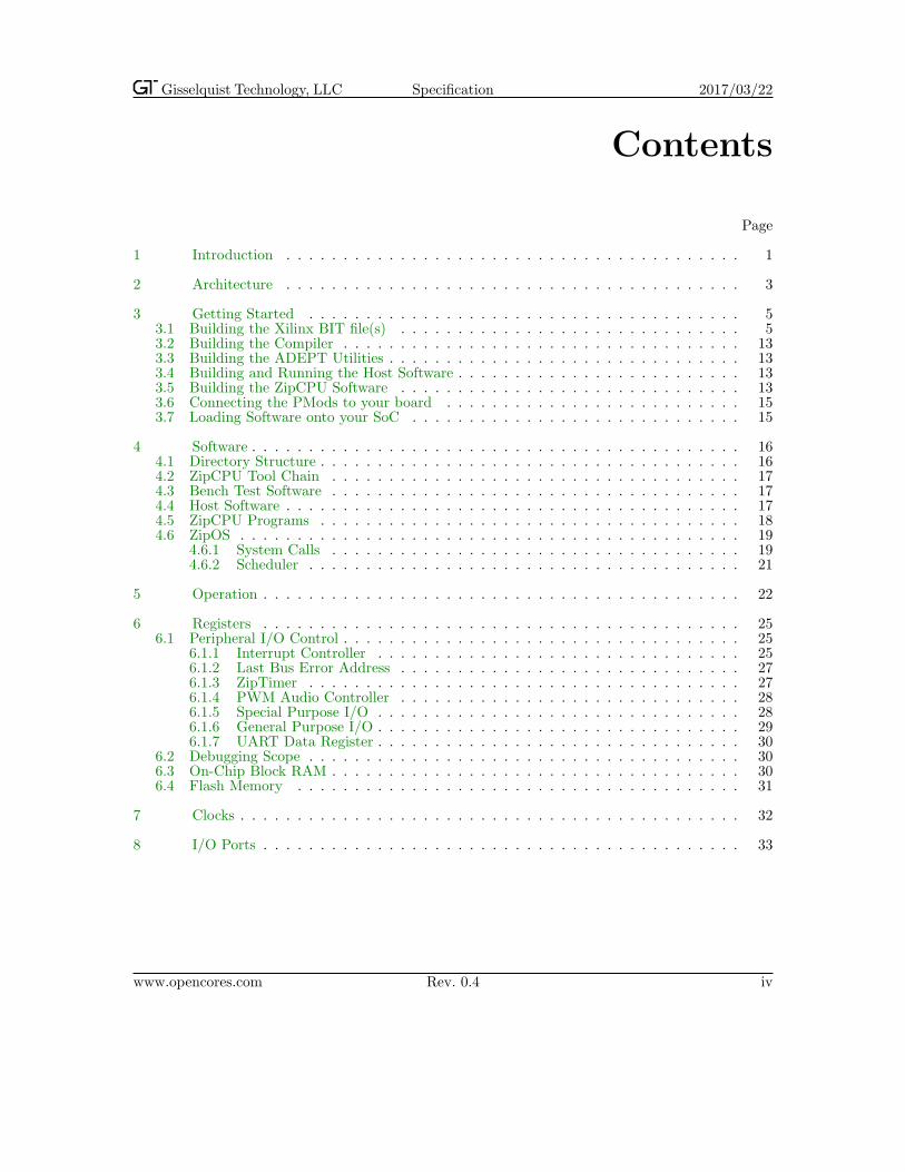
1 Introduction . . . . . . . . . . . . . . . . . . . . . . . . . . . . . . . . . . . . . . . . 1
2 Architecture . . . . . . . . . . . . . . . . . . . . . . . . . . . . . . . . . . . . . . . . 3
3 Getting Started . . . . . . . . . . . . . . . . . . . . . . . . . . . . . . . . . . . . . . 53.1 Building the Xilinx BIT file(s) . . . . . . . . . . . . . . . . . . . . . . . . . . . . . . 53.2 Building the Compiler . . . . . . . . . . . . . . . . . . . . . . . . . . . . . . . . . . . 133.3 Building the ADEPT Utilities . . . . . . . . . . . . . . . . . . . . . . . . . . . . . . . 133.4 Building and Running the Host Software . . . . . . . . . . . . . . . . . . . . . . . . . 133.5 Building the ZipCPU Software . . . . . . . . . . . . . . . . . . . . . . . . . . . . . . 133.6 Connecting the PMods to your board . . . . . . . . . . . . . . . . . . . . . . . . . . 153.7 Loading Software onto your SoC . . . . . . . . . . . . . . . . . . . . . . . . . . . . . 15
4 Software . . . . . . . . . . . . . . . . . . . . . . . . . . . . . . . . . . . . . . . . . . . 164.1 Directory Structure . . . . . . . . . . . . . . . . . . . . . . . . . . . . . . . . . . . . . 164.2 ZipCPU Tool Chain . . . . . . . . . . . . . . . . . . . . . . . . . . . . . . . . . . . . 174.3 Bench Test Software . . . . . . . . . . . . . . . . . . . . . . . . . . . . . . . . . . . . 174.4 Host Software . . . . . . . . . . . . . . . . . . . . . . . . . . . . . . . . . . . . . . . . 174.5 ZipCPU Programs . . . . . . . . . . . . . . . . . . . . . . . . . . . . . . . . . . . . . 184.6 ZipOS . . . . . . . . . . . . . . . . . . . . . . . . . . . . . . . . . . . . . . . . . . . . 19
4.6.1 System Calls . . . . . . . . . . . . . . . . . . . . . . . . . . . . . . . . . . . . 194.6.2 Scheduler . . . . . . . . . . . . . . . . . . . . . . . . . . . . . . . . . . . . . . 21
5 Operation . . . . . . . . . . . . . . . . . . . . . . . . . . . . . . . . . . . . . . . . . . 22
6 Registers . . . . . . . . . . . . . . . . . . . . . . . . . . . . . . . . . . . . . . . . . . 256.1 Peripheral I/O Control . . . . . . . . . . . . . . . . . . . . . . . . . . . . . . . . . . . 25
6.1.1 Interrupt Controller . . . . . . . . . . . . . . . . . . . . . . . . . . . . . . . . 256.1.2 Last Bus Error Address . . . . . . . . . . . . . . . . . . . . . . . . . . . . . . 276.1.3 ZipTimer . . . . . . . . . . . . . . . . . . . . . . . . . . . . . . . . . . . . . . 276.1.4 PWM Audio Controller . . . . . . . . . . . . . . . . . . . . . . . . . . . . . . 286.1.5 Special Purpose I/O . . . . . . . . . . . . . . . . . . . . . . . . . . . . . . . . 286.1.6 General Purpose I/O . . . . . . . . . . . . . . . . . . . . . . . . . . . . . . . . 296.1.7 UART Data Register . . . . . . . . . . . . . . . . . . . . . . . . . . . . . . . . 30
6.2 Debugging Scope . . . . . . . . . . . . . . . . . . . . . . . . . . . . . . . . . . . . . . 306.3 On-Chip Block RAM . . . . . . . . . . . . . . . . . . . . . . . . . . . . . . . . . . . . 306.4 Flash Memory . . . . . . . . . . . . . . . . . . . . . . . . . . . . . . . . . . . . . . . 31
7 Clocks . . . . . . . . . . . . . . . . . . . . . . . . . . . . . . . . . . . . . . . . . . . . 32
8 I/O Ports . . . . . . . . . . . . . . . . . . . . . . . . . . . . . . . . . . . . . . . . . . 33
www.opencores.com Rev. 0.4 iv
Gisselquist Technology, LLC Specification 2017/03/22
Figures
Figure Page
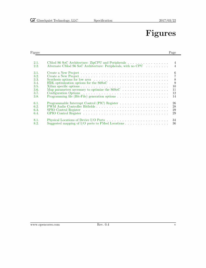
2.1. CMod S6 SoC Architecture: ZipCPU and Peripherals . . . . . . . . . . . . . . . . 42.2. Alternate CMod S6 SoC Architecture: Peripherals, with no CPU . . . . . . . . . 4
3.1. Create a New Project . . . . . . . . . . . . . . . . . . . . . . . . . . . . . . . . . . 63.2. Create a New Project . . . . . . . . . . . . . . . . . . . . . . . . . . . . . . . . . . 73.3. Synthesis options for low area . . . . . . . . . . . . . . . . . . . . . . . . . . . . . 83.4. HDL optimization options for the S6SoC . . . . . . . . . . . . . . . . . . . . . . . 93.5. Xilinx specific options . . . . . . . . . . . . . . . . . . . . . . . . . . . . . . . . . . 103.6. Map parameters necessary to optimize the S6SoC . . . . . . . . . . . . . . . . . . 113.7. Configuration Options . . . . . . . . . . . . . . . . . . . . . . . . . . . . . . . . . 123.8. Programming file (Bit-File) generation options . . . . . . . . . . . . . . . . . . . . 14
6.1. Programmable Interrupt Control (PIC) Register . . . . . . . . . . . . . . . . . . . 266.2. PWM Audio Controller Bitfields . . . . . . . . . . . . . . . . . . . . . . . . . . . . 286.3. SPIO Control Register . . . . . . . . . . . . . . . . . . . . . . . . . . . . . . . . . 296.4. GPIO Control Register . . . . . . . . . . . . . . . . . . . . . . . . . . . . . . . . . 29
8.1. Physical Locations of Device I/O Ports . . . . . . . . . . . . . . . . . . . . . . . . 348.2. Suggested mapping of I/O ports to PMod Locations . . . . . . . . . . . . . . . . . 36
www.opencores.com Rev. 0.4 v
Gisselquist Technology, LLC Specification 2017/03/22
Tables
Table Page
6.1. Address Regions . . . . . . . . . . . . . . . . . . . . . . . . . . . . . . . . . . . . . 256.2. I/O Peripheral Registers . . . . . . . . . . . . . . . . . . . . . . . . . . . . . . . . 266.3. Hardware Interrupts . . . . . . . . . . . . . . . . . . . . . . . . . . . . . . . . . . . 276.4. Flash Address Regions . . . . . . . . . . . . . . . . . . . . . . . . . . . . . . . . . 31
8.1. List of IO ports . . . . . . . . . . . . . . . . . . . . . . . . . . . . . . . . . . . . . 33
www.opencores.com Rev. 0.4 vi
Gisselquist Technology, LLC Specification 2017/03/22
Preface
The ZipCPU was built with the express purpose of being an area optimized, 32–bit FPGA softprocessor.
The S6 SoC is designed to prove that the ZipCPU has met this goal.There are two side–effects to this. First, the project proves how capable a very small FPGA, such
as the Spartan 6/LX4 on the CMod–S6, can be and second, this project provides demonstrationimplementations of how to interact with a variety of PMod devices: the audio amplifier, the serial2–line LCD display, the USBUART, and the 16–character numeric keypad.
Dan Gisselquist, Ph.D.
www.opencores.com Rev. 0.4 vii
Gisselquist Technology, LLC Specification 2017/03/22
1.
Introduction
The ZipCPU is a soft core Central Processing Unit (CPU) designed to fit within an FPGA, to usea minimum amount of the FPGA’s resources, and yet to still provide the services of a fully capable32–bit computer. It is based upon a Von Neumann architecture and so a single 32–bit wishbone busprovides it with access to both peripherals and memory.
Previous demonstrations of the ZipCPU have focused on larger FPGAs, such as the Spartan–6LX9 and LX25 and the Artix–7 35T. On these FPGA’s, the ZipCPU runs in a pipelined configurationwhere it is tightly integrated with a prefetch/instruction cache. While these demonstrations haveshown that the ZipCPU can act as a very simple CPU in these environments, they really haven’tdemonstrated the ability of the ZipCPU to use only a minimum amount of the FPGA’s resources.
The CMod S6 board provides the opportunity for that demonstration rather nicely.
1. The Spartan–6 LX4 FPGA is very limited in its resources: It only has 2,400 look–up tables(LUTs), and can only support a 16 kB RAM memory.
2. With only 16kB RAM, the majority of any program will need to be placed into and run fromthe flash.
3. While the chip has enough area for the CPU, it doesn’t have enough area to include the CPUand . . . write access to the flash, debug access, wishbone command access from the UART,pipelined CPU operations, a prefetch cache and more. Other solutions will need to be foundas part of this project.
Of course, if someone just wants the functionality of a small, cheap, CPU, this project doesnot fit that role very well. While the S6 is not very expensive at nearly $70, it is still an order ofmagnitude greater than it’s CPU competitors in price. This includes such CPU’s as the RaspberryPi Zero ($5), or even the TeensyLC ($12).
If, on the other hand, what you want is a small, cheap, CPU that can be embedded withinan FPGA without using too much of the FPGA’s resources, this project will demonstrate thatpossibility as well as showing that the CPU even has some utility. Alternatively, if you wish tostudy how to get a CPU to work in a small, constrained environment, this project may be whatyou are looking for. Likewise, if you are a software developer forced to get something running on anFPGA, such as the CMod-S6, you may have just found your answer.
Finally, because the ZipCPU and the included ZipOS are as small and simple as they are, thecode base found here will be simpler to understand than the code bases for some of these otherprojects. For example, the ZipCPU instruction set is very simple. With only 29 instructions, it ismuch easier to understand and learn than the ARM instruction set. Further, unlike the ARM, theentire specification for and description of the ZipCPU is publicly available. Likewise, an operating
www.opencores.com Rev. 0.4 1

Gisselquist Technology, LLC Specification 2017/03/22
system such as the ZipOS that has less than 3,000 lines of code will be much easier to understandthan any Linux operating system–even if it has much less functionality.1
1I’m still entertaining thoughts of placing Linux onto this device.
www.opencores.com Rev. 0.4 2
Gisselquist Technology, LLC Specification 2017/03/22
2.
Architecture
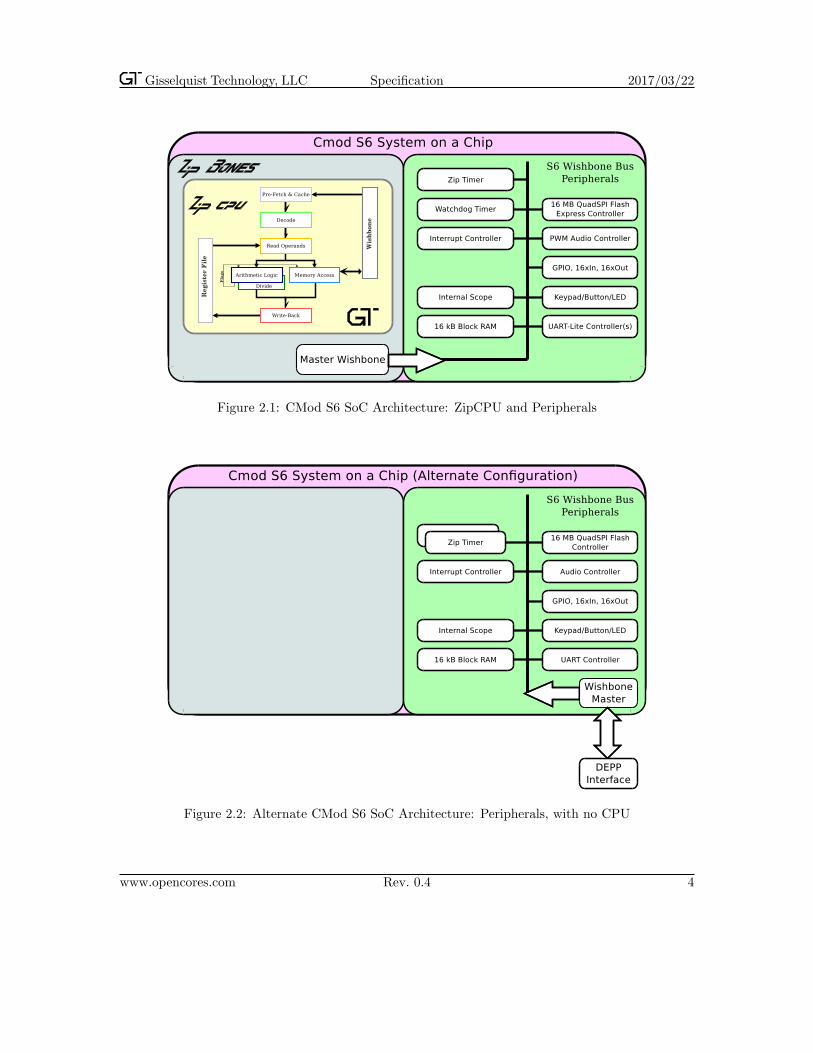
Fig. 2.1 shows the basic internal architecture of the S6 SoC. In summary, it consists of a CPUcoupled with a variety of peripherals for the purpose of controlling the external peripherals of theS6 SoC: flash, LEDs, buttons, and GPIO. External devices may also be added on, and have beenadded on as part of this project, such as an audio device, an external serial port, an external keypad,and an external display. All of these devices are then available for the CPU to interact with.
If you are familiar with the ZipCPU, you’ll notice this architecture provides no access to theZipCPU debug port. There simply wasn’t enough room on the device. Debugging the ZipCPU willinstead need to take place via other means, such as dumping all registers and/or memory to theserial port on any reboot, and making judicious use of the internal scope.
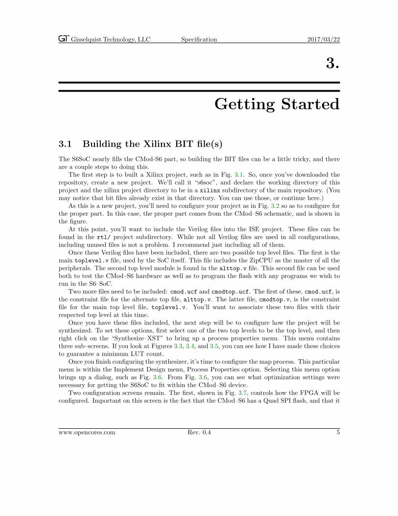
Further, the read/write flash controller couldn’t fit in the design along with the ZipCPU, leavingthe ZipCPU with a simpler read–only flash controller and no ability to write to flash memory. Forthis reason, there exists an alternate CMod S6 SoC architecture, shown in Fig. 2.2. Using thisalternate architecture, it is be possible to test the peripherals and program the flash memory.
The basic approach to loading the board is actually quite simple. Using the Digilent ADEPTJTAG configuration program, djtgcfg, the alternate configuration may be written directly to thedevice. Once this alternate configuration has been loaded, the flash may be examined and pro-grammed using the zipload utility. This utility uses Digilent’s Asynchronous Parallel Port interface(DEPP) to communicate with the device, and in particular to tell the device what to write to theflash. When writing to the flash, the zipload utility can program the FPGA configuration into theconfiguration section of the flash, as well as computer code into the rest of the flash. Once com-plete, the system may then be reloaded, either by power down/up or via djtgcfg, with the primaryconfiguration file which will contain an image of the CPU. The CPU will then begin following theinstructions found in flash memory.
www.opencores.com Rev. 0.4 3
Gisselquist Technology, LLC Specification 2017/03/22
Figure 2.1: CMod S6 SoC Architecture: ZipCPU and Peripherals
Figure 2.2: Alternate CMod S6 SoC Architecture: Peripherals, with no CPU
www.opencores.com Rev. 0.4 4
Gisselquist Technology, LLC Specification 2017/03/22
3.
Getting Started
3.1 Building the Xilinx BIT file(s)
The S6SoC nearly fills the CMod-S6 part, so building the BIT files can be a little tricky, and thereare a couple steps to doing this.
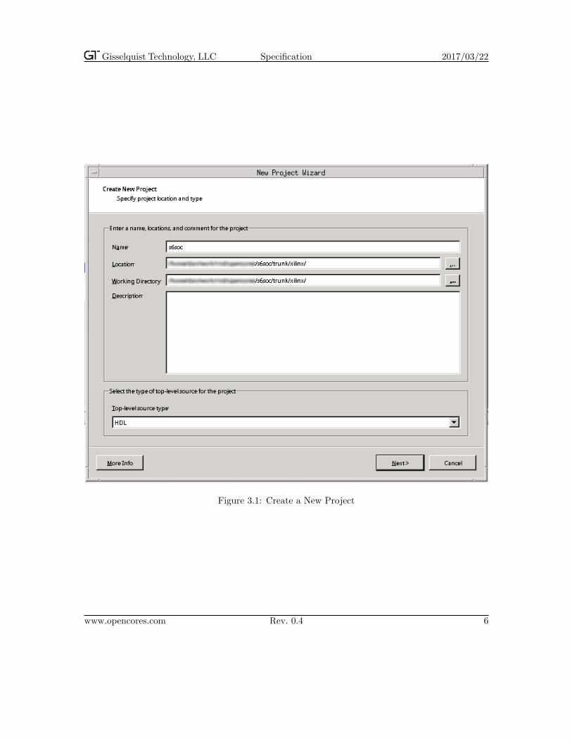
The first step is to built a Xilinx project, such as in Fig. 3.1. So, once you’ve downloaded therepository, create a new project. We’ll call it “s6soc”, and declare the working directory of thisproject and the xilinx project directory to be in a xilinx subdirectory of the main repository. (Youmay notice that bit files already exist in that directory. You can use those, or continue here.)
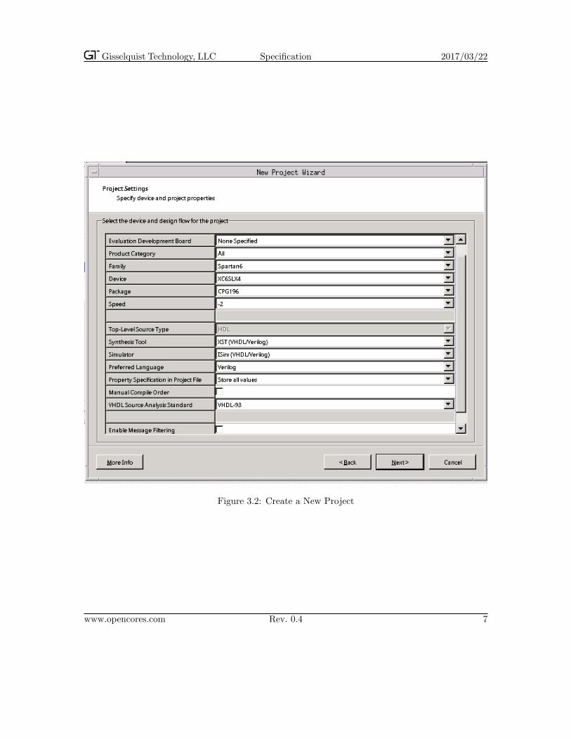
As this is a new project, you’ll need to configure your project as in Fig. 3.2 so as to configure forthe proper part. In this case, the proper part comes from the CMod–S6 schematic, and is shown inthe figure.
At this point, you’ll want to include the Verilog files into the ISE project. These files can befound in the rtl/ project subdirectory. While not all Verilog files are used in all configurations,including unused files is not a problem. I recommend just including all of them.
Once these Verilog files have been included, there are two possible top level files. The first is themain toplevel.v file, used by the SoC itself. This file includes the ZipCPU as the master of all theperipherals. The second top level module is found in the alttop.v file. This second file can be usedboth to test the CMod–S6 hardware as well as to program the flash with any programs we wish torun in the S6–SoC.
Two more files need to be included: cmod.ucf and cmodtop.ucf. The first of these, cmod.ucf, isthe constraint file for the alternate top file, alttop.v. The latter file, cmodtop.v, is the constraintfile for the main top level file, toplevel.v. You’ll want to associate these two files with theirrespected top level at this time.
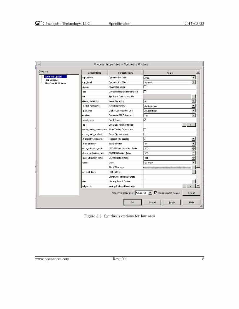
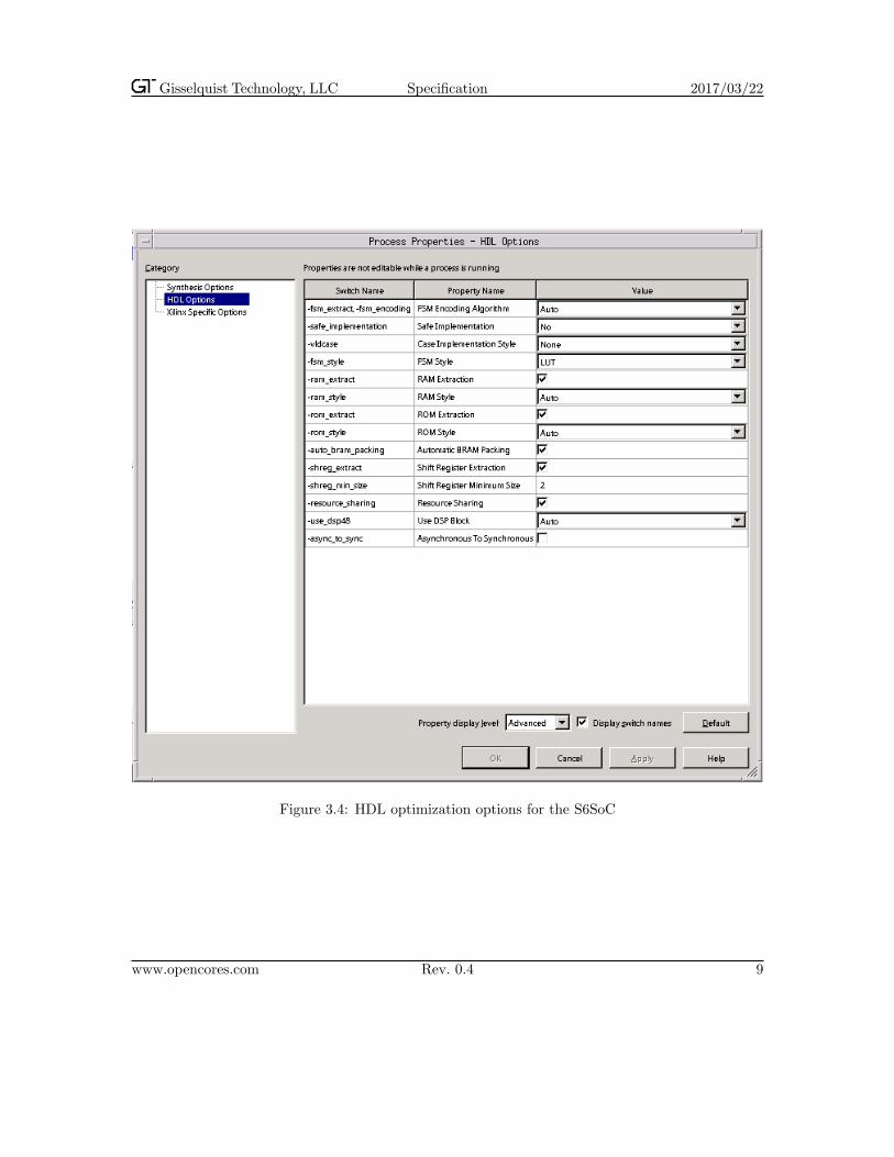
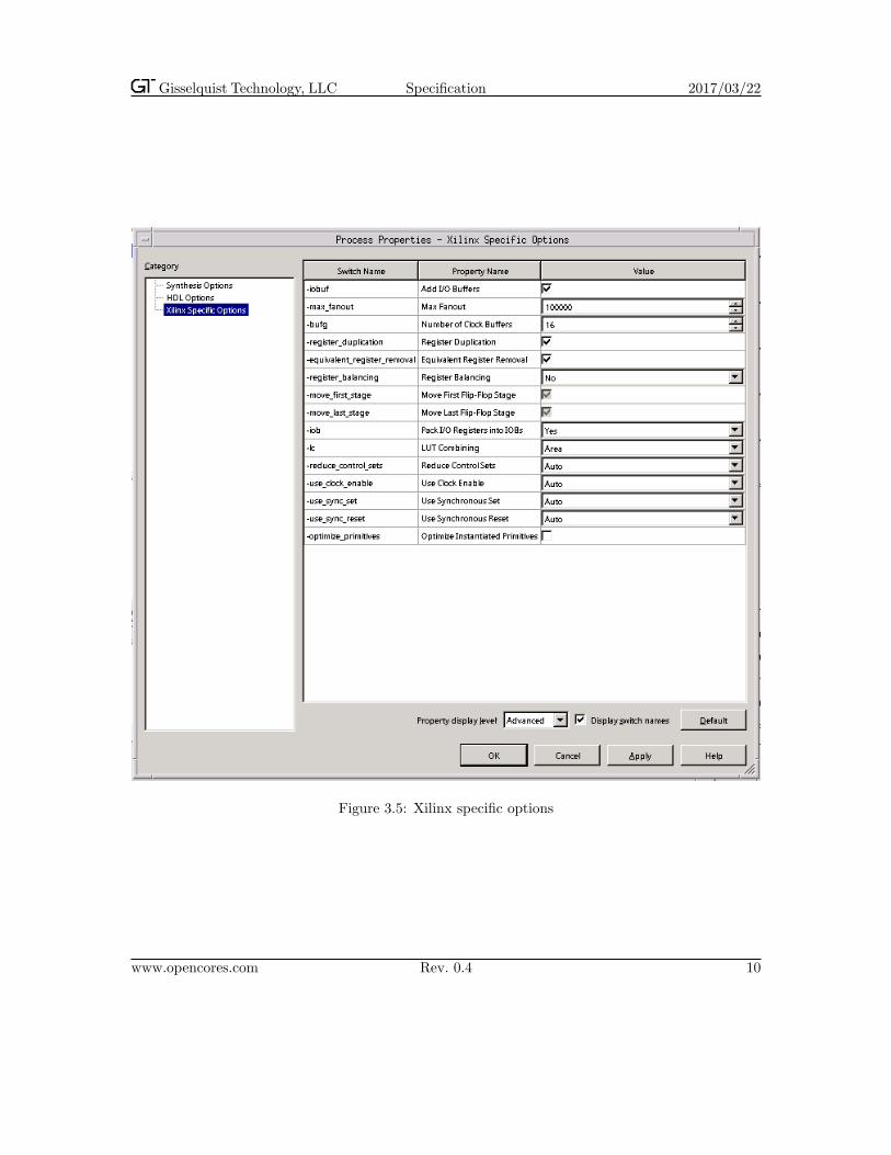
Once you have these files included, the next step will be to configure how the project will besynthesized. To set these options, first select one of the two top levels to be the top level, and thenright click on the “Synthesize–XST” to bring up a process properties menu. This menu containsthree sub–screens. If you look at Figures 3.3, 3.4, and 3.5, you can see how I have made these choicesto guarantee a minimum LUT count.
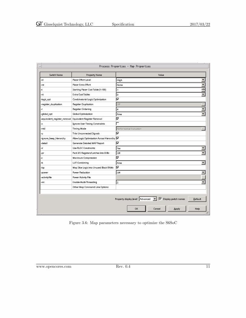
Once you finish configuring the synthesizer, it’s time to configure the map process. This particularmenu is within the Implement Design menu, Process Properties option. Selecting this menu optionbrings up a dialog, such as Fig. 3.6. From Fig. 3.6, you can see what optimization settings werenecessary for getting the S6SoC to fit within the CMod–S6 device.
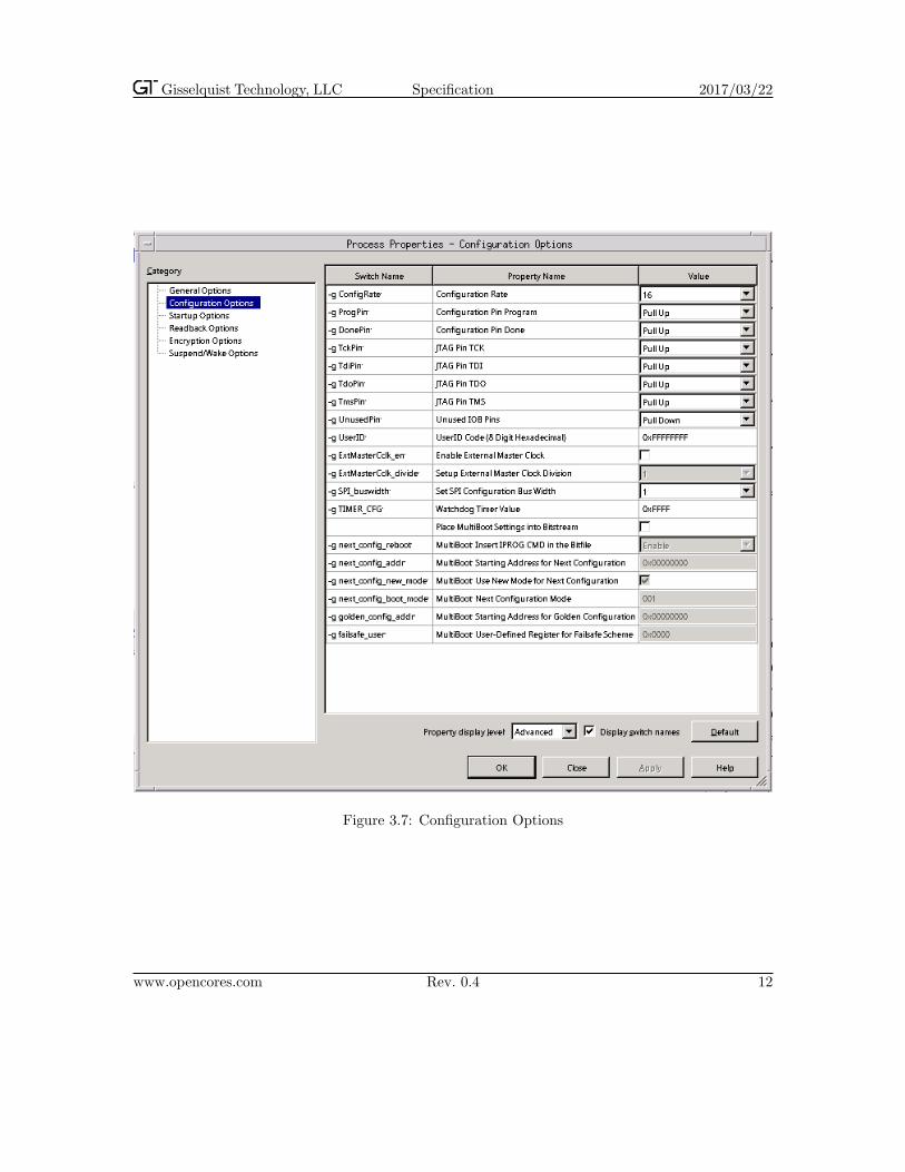
Two configuration screens remain. The first, shown in Fig. 3.7, controls how the FPGA will beconfigured. Important on this screen is the fact that the CMod–S6 has a Quad SPI flash, and that it
www.opencores.com Rev. 0.4 5
Gisselquist Technology, LLC Specification 2017/03/22
Figure 3.1: Create a New Project
www.opencores.com Rev. 0.4 6
Gisselquist Technology, LLC Specification 2017/03/22
Figure 3.2: Create a New Project
www.opencores.com Rev. 0.4 7
Gisselquist Technology, LLC Specification 2017/03/22
Figure 3.3: Synthesis options for low area
www.opencores.com Rev. 0.4 8
Gisselquist Technology, LLC Specification 2017/03/22
Figure 3.4: HDL optimization options for the S6SoC
www.opencores.com Rev. 0.4 9
Gisselquist Technology, LLC Specification 2017/03/22
Figure 3.5: Xilinx specific options
www.opencores.com Rev. 0.4 10
Gisselquist Technology, LLC Specification 2017/03/22
Figure 3.6: Map parameters necessary to optimize the S6SoC
www.opencores.com Rev. 0.4 11
Gisselquist Technology, LLC Specification 2017/03/22
Figure 3.7: Configuration Options
www.opencores.com Rev. 0.4 12
Gisselquist Technology, LLC Specification 2017/03/22
can be run from a clock as fast as 108 MHz. Here, we choose 16 MHz although I know of no reasonwhy the clock speed could not be made faster.
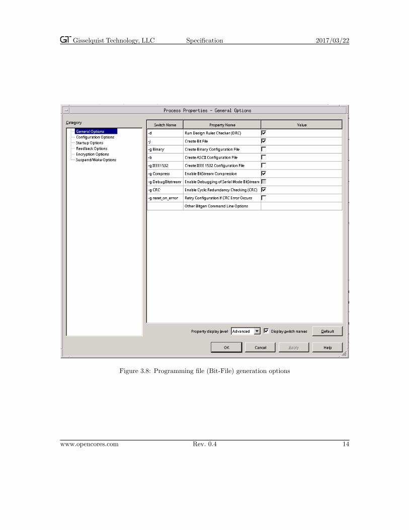
As a final configuration screen, there are options for generating the programming (bit) file. Theseare shown in Fig. 3.8. From the standpoint of the CMod–S6, the important configuration item hereis that we would like to compress the bit file, so that we can pack as much information into our flashdevice as possible.
Having gone through all of your configuration options, you may now build the two configurations,toplevel.bit and alttop.bit which are used in this distribution.
make axload in the main directory (assuming the Digilent ADEPT utilities are installed) willload the alternate configuration into the flash, while make xload will load the main configurationinto the flash. For our purposes, and until you have a compiled program to run, you will want toload the alternate configuration into the flash.
3.2 Building the Compiler
The ZipCPU compiler comes as source from the ZipCPU distribution. To build this compiler, clonethe ZipCPU distribution and follow the build and installation instructions within it. Ever afterwards,you’ll want the ZipCPU toolchain, zip-gcc, zip-as, zip-ld, etc., in your path.1
3.3 Building the ADEPT Utilities
You will also need a copy of Digilent’s ADEPT software installed on your system in order to usethe CMod–S6. This includes not only the ADEPT utilities, but also ADEPT software developmentkit and it’s runtime environment. We’ll need these pieces of software to provide both the djtgcfg
program to load the FPGA with our designs, as well as the DEPP port, provided by both the SDKand the runtime environment, necessary to communicate with our board.
3.4 Building and Running the Host Software
Once you have the ADEPT utilities installed, you may then build the software in the sw/host projectsubdirectory. The makefile in this directory has a reference to the location of ADEPT include files,which you may need to update according to where you have installed ADEPT. You may also needto adjust the library path, so that it properly references the ADEPT libraries. (The library path iscurrently hard coded into the Makefile.)
3.5 Building the ZipCPU Software
Once you have the ZipCPU toolchain built, you may then build the ZipCPU software which will beplaced onto the board. This software may be found in the sw/dev directory. The ZipOS examplecan be found in the sw/zipos directory. A make command executed in each of these directoriesshould build the ZipCPU software for the board.
1You may need to install several packages to do this, such as: flex, bison, libbison-dev, libgmp10, libgmp-dev,
libmpfr-dev, libmpc-dev, libelf-dev, ncurses-dev, libelf-dev, and verilator.
www.opencores.com Rev. 0.4 13
Gisselquist Technology, LLC Specification 2017/03/22
Figure 3.8: Programming file (Bit-File) generation options
www.opencores.com Rev. 0.4 14

Gisselquist Technology, LLC Specification 2017/03/22
3.6 Connecting the PMods to your board
The S6 SoC supports four PMods: The PModUSBUART, the PModAMP2 pwm to audio amplifier,the PModCLS two line LCD display, and the PModKYPD sixteen character keypad. These need tobe wired up to the CMod S6 as shown in Fig. 8.2 on page 36.
3.7 Loading Software onto your SoC
Once you have all the software loaded, you may wish to try a simple LED program. You may findthe sw/dev/blinky.c program suitable for this purpose. To run this program, you will need tofollow a series of steps:
1. Build the sw/dev/blinky program.
2. Build both Xilinx configurations, alttop.bit and toplevel.bit. The main makefile will lookfor these files in the xilinx/ project subdirectory that you made when you created the project.
3. From the main project subdirectory, run make axload to load the alternate configuration ontoyour board. (You do have your board plugged in, right?)
4. Then you can run the zipload program found in the sw/host directory. zipload takes oneor two arguments. In this example, we’ll give it a first argument of the xilinx/toplevel.bitfile, and a second argument of the program we would like to run, sw/dev/blinky.
5. Assuming zipload completed successfully, you can then either run make xload from the maindirectory, or you may remove and reconnect power to your board.
6. A blinking light demonstration should now be running on your board.
www.opencores.com Rev. 0.4 15
Gisselquist Technology, LLC Specification 2017/03/22
4.
Software
This chapter provides an overview of the software that is available to support the S6 SoC. Thisincludes not only the RTL, the Makefiles, and the software that will run on the ZipCPU within theS6 SoC, but also the support software necessary for communicating with the S6 SoC in its alternateconfiguration.
4.1 Directory Structure
sim/verilator/ Contains software for emulating the S6 SoC without the S6 present.
All of the bench testing software is written in C++, so it is found in this directory. Primaryamong these programs is the zip sim program which will simulate the ZipCPU within theS6 SoC. Specifically, it simulates everything at or below the busmaster.v level.
Some, although not all, of the peripherals have been simulated and made a part of this simu-lation. These include the Quad–SPI flash, the UART, the LED’s and the GPIOs.
doc/ All of the documentation for the S6 SoC project may be found in this documentation directory.Specifically, I would commend your attention to anything with a .pdf extension, as these arethe completed documents. Among these you should find a copy of the GPL copyright underwhich this software is released, as well as a pre–built copy of this document.
doc/gfx/ Here is where the graphics are located in support of this specification document.
doc/src/ And here is where the LATEXfiles are kept that were used in building both this documentas well as the GPL copyright.
rtl/ Verilog files. The two top–level files are toplevel.v for the primary top level module, andalttop.v for the alternate load.
rtl/cpu Verilog files containing the ZipCPU core and peripherals. The toplevel file here is thezipbones.v file, although some of the peripherals, such as the ziptimer.v are referencedindependently.
sw/ The main software directory, primarily a repository for software subdirectories beneath it.
sw/dev/ This directory holds a variety of simple programs for the ZipCPU, such as blinky,helloworld, doorbell and doorbell2, as well as software drivers for various periph-erals, such as the real–time clock simulator, and the keypad and display device drivers.
One key file in this directory is the cputest.c file, which provides a basic test of theCPU and its capabilities.
www.opencores.com Rev. 0.4 16
Gisselquist Technology, LLC Specification 2017/03/22
sw/host/ This directory holds support software which can be built on and run on the host machine.Building this software will involve adjusting the Makefile so that it knows where yourlocal ADEPT installation directory is. Once built, you will find a variety of very usefulprograms within here.
sw/zipos/ This directory contains the source code for a rudimentary, very basic, pre-emptive multi-tasking operating system that I call the ZipOS.
4.2 ZipCPU Tool Chain
To build programs for the ZipCPU, you will need the ZipCPU toolchain. You can find this as partof the ZipCPU project, available at OpenCores. Building the ZipCPU project should result in a setof binaries in the sw/install/cross-tools/bin/ subdirectory of your ZipCPU project directory.Make this directory a part of your path, and you should be able to build the CMod S6 ZipCPUsoftware. Specifically, you will need to use zip-gcc, zip-as, zip-ld, and zip-cpp. Other tools,such as zip-objdump and zip-readelf, may also prove to be very useful when trying to debug whatis going on within the SoC.
4.3 Bench Test Software
Bench testing software currently consists of the zip sim program found within sim/verilator. Thisprogram requires Verilator to run, and simulates in a cycle accurate fashion, the entire S6 SoC frombusmaster.v on down. Further, the external Quad–SPI flash memory, UART, and LED’s are alsosimulated, although the 2–line display, audio, and keypad are not.
4.4 Host Software
Several software programs have been built to support the S6 SoC from a nearby host. These programsinclude:
• dumpuart: My current approach to debugging involves dumping the state of the registers andmemory to the UART upon reboot. The dumpuart command found here is designed to makecertain that the UART is first set up correctly at 9600 Baud, and second that everything readfrom the UART is directly sent to both a file and to the screen. In this fashion, it is similarto the UNIX tee program, save for its serial port attachment.
• readflash: As I am loathe to remove anything from a device that came factory installed, thereadflash program reads the original installed configuration from the flash and dumps it toa file.
This program is only useful when the alternate configuration is loaded.
• wbregs: This program offers a capability very similar to the PEEK and POKE capabilityApple user’s may remember from before the days of Macintosh. wbregs <address> will readfrom the Wishbone bus the value at the given address. Likewise wbregs <address> <value>
will write the given value into the given address. While both address and value have the
www.opencores.com Rev. 0.4 17
Gisselquist Technology, LLC Specification 2017/03/22
semantics of numbers acceptable to strtoul(), the address can also be a named address.Supported names can be found in regdefs.cpp, and their register mapping in regdefs.h.
As examples, wbregs version, will return the build date, or version of the RTL. wbregs spio
reads the special purpose I/O register, and wbregs gpio 0xffffffff will set all output GPIOports high while wbregs gpio 0xffff0000 will set all output GPIO ports to ground.
This program is only useful when the alternate configuration is loaded. When the primarytoplevel.v configuration is loaded, the ZipCPU will be able to read and write these registersin a similar fashion.
• zipload: This is the primary program you will need to get your software loaded on the CMod.It takes two arguments. The first is the name of the primary Xilinx configuration file, and thesecond is the name of the ZipCPU program you wish to write to Flash memory.
Each of these arguments is optional. For example, if a configuration file is given, the loaderwill load the primary configuration. If a ZipCPU program is given, the program will be loadedinto the program memory area and the configuration file areas will be left untouched.
As with wbregs, this program is only useful when the alternate configuration is loaded.
4.5 ZipCPU Programs
The following are a list of simple, independent, single-task example programs that will run on theS6 SoC:
• blinky: This is a very simple program similar to hello world, with the difference that the lightshave a bit of a different response, the hello world message is written slower, and interrupts areused to accomplish this purpose.
• helloworld: The first program any programmer should build, “Hello, world!” This programsends the string, “Hello, world!” over the UART connection once per second. It is a veryvaluable program because, if you can get this program running, you know you have a lot ofthings working and working correctly. For example, running this program means you can runthe zip-gcc compiler, load the auxiliary configuration, load the program info flash memory,load the primary configuration, and read from the UART port. It also means that you musthave the UART port properly configured and wired to your CMod board.
Unlike other versions of Hello World that you may be familiar with, this one does not use theC–library. It programs the hardware directly.
• cputest: This is a simple test of the CPU and all of its functionality. The functionalityproven is primarily assembly level, but it does require the C compiler to put its frameworktogether. cputest is actually one of two programs built from the same source. The otheris named cputestcis, and specifically allows the complex instruction set (CIS) instructionswhereas cputest specifically disallows them. The difference, therefore, is in the command lineparameters given to the assembler (via the compiler).
• doorbell: This annoying program verifies the functionality of the audio device by playing adoorbell sound to the audio port. It will then wait ten seconds, and play the doorbell soundagain (and again, and again). (It gets old after a while ...)
www.opencores.com Rev. 0.4 18
Gisselquist Technology, LLC Specification 2017/03/22
• doorbell2: This adds to the functionality of the doorbell program a wait for keypress, anda display of the current time on the 2–line display. While almost our fully functional ZipOSprogram, this does not include any menus to configure the device or set time, since it doesn’tinclude any keypad functionality.
• kptest: A test of whether or not they keypad driver works. When run, anytime a key ispressed, the key’s associated printable character will be sent to the UART. Further, pressingan ‘F’ on the keypad will also send a newline over the UART, in case you wish to keep yourlines from getting too long.
4.6 ZipOS
The ZipOS is a brand new operating system, specifically designed to run on the ZipCPU. It is bothpre–emptive and multitasking, although with many limitations. Those familiar with the internalsof other operating systems, such as Linux, may laugh that I call this an Operating System at all:it has no memory management unit, no paging, no virtual memory, no file I/O access, no networkstack, no ability to dynamically add or remove tasks, indeed it hardly has any of the things mostoften associated with an Operating System. It does, however, handle interrupts, support multiplepre–emptive tasks in a multitasking, timesharing fashion, and it supports some very basic andrudimentary system calls. In a similar fashion, it does contain just about all of the functionalitynecessary for a multi–tasking microcontroller built around a do–forever loop. For its size, I considerit an impressive achievement. You are welcome to disagree with me.
This version of the ZipOS starts in the resetdump.s code, so that upon any startup the ZipOSwill dump register contents, the BusError register, and any scope contents to the UART–assumingthat the scope had been triggered. This can take some time, so you may wish to configure what youreally wish to send–if anything. If desired, resetdump can be configured to also dump the entirememory as well while only using ten memory locations in its own support. All of this is quite usefulin case the ZipCPU encounters a bus error or other sort of error that causes it to hang, stall, orreboot, as the CPU registers are very carefully not touched prior to being sent to the UART outputport. This extends to all registers save the supervisor PC and CC registers, which would’ve beenreset by a reboot anyway.
resetdump.s then calls a rudimentary bootloader, to load the parts of the ZipOS that need torun faster into Block RAM. The choice of what parts to load into Block RAM is made on a file byfile basis, and found within the linker script, cmodram.ld.
Upon completion, resetdump.s calls the entry routine for the O/S, kernel entry() found inkernel.c. This is the main task loop for the entire O/S, and worth studying if you are interestedin understanding how the O/S works.
The user tasks are found (mostly) within doorbell.c, also found in the ZipOS directory. Thisfile contains two kernel entry points, kntasks(), which returns the number of user tasks the kernelneeds to know about, and kinit(), which builds each of the tasks and connects their file descriptorsto the various devices they will be referencing.
4.6.1 System Calls
The ZipOS supports a variety of system calls, listed here:
www.opencores.com Rev. 0.4 19
Gisselquist Technology, LLC Specification 2017/03/22
• int wait(unsigned event mask, int timeout)
Halts the execution of a process until an event matching the event mask takes place, or atimeout (in milliseconds) has been reached. The events that can take place are a bitmask ofthe various interrupts the CPU supports, together with a bitmask of the software interruptvalues found in swint.h.
The timeout value can either be zero, to return immediately with the list of events that havetaken place, negative, to wait indefinitely, or a positive number of milliseconds in order to waitat least that time for the event of interest to take place.
Waiting on a zero event mask allows a process to sleep for any number of requested milliseconds.
When wait returns, any events returned by the wait have been cleared.
The other thing to be aware of is that events may accumulate before the wait system call.Nothing within the wait system call clears prior events. These prior events be returned andcleared, though, if the wait call indicates an interest in those events.
Upon return, the a bitmask of events that have taken place will be returned to the process.
• int clear(unsigned event mask, int timeout)
This system call works closely with the wait system call. Indeed, when the timeout given iszero, the two function nearly identically. It clears any of the requested events which may bepending, and returns a bit mask of the events that were pending and cleared.
However, if the timeout is given (and is positive), then clear() starts a timer. Once the timerhas completed, a timeout event, SWINT TIMEOUT, will be generated and made available to thetask to wait upon it.
In a similar fashion, if the timeout is negative, then any pending timeout is cleared.
• void post(unsigned event mask)
Certain software devices, such as the real–time clock and the doorbell reader, need the abilityof being able to post events to any listener within the O/S. The POST system call allows themto POST events in this manner.
Were the ZipOS to be closer to a secure O/S, it might restrict what events each process couldpost. Right now, however, any process can post any event–whether it be a hardware or asoftware generated event.
• void yield(void)
This is simply a way of being nice to other processes. This system call takes no argumentsand simply asks the scheduler to schedule the next process. It does not take this process offof the ready to run list, so the next process may be this one. However, since the scheduler isa round–robin scheduler, it will only return to this process once it has gone through all otheravailable processes checking whether or not they are available to be run.
• int read(int fid, void *buf, int len)
This is roughly the same system call as the POSIX read() system call. It reads some number ofwords (not octets) from the file descriptor (device) specified by fid into the memory address
www.opencores.com Rev. 0.4 20
Gisselquist Technology, LLC Specification 2017/03/22
range starting at buf and len words long. If the memory requested is unavailable, the readwill wait until it is available, possibly indefinitely.
Upon return, the read() function call returns the number of words actually read, or a negativevalue on error.
As a future feature, a read() system call should be able to be interrupted by a timeout. Thisfeature has not (yet) been implemented, but will likely be implemented via a combination ofthe clear() system calls ability to set timeouts together with the read() functions ability towait for available data.
• int write(int fid, void *buf, int len)
This is roughly the same system call as the POSIX write() system call. It writes some numberof memory addresses (words, not octets), to the given file descriptor. If there is no reader taskor device associated with the file descriptor, then the write() system call will block foreveronce the internal pipe fills up. Otherwise, if something is reading from the file descriptor’spipe, the writing task will only stall until the data is either written to the receiving task, orcopied into a memory buffer.
Upon return, the write() system call returns the number of words actually written to thesystem pipe (not necessarily the number that have been read), or a negative value on error.
• unsigned time(void)
Returns the number of seconds since startup. Eventually, this will return the number of secondssince January 1, 1970, and be identical to the UNIX system time() command, but that maynot happen on this project.
• void *malloc(void)
Allocates memory from the system/kernel heap. This is a very low overhead memory allocatorthat, while it does allocate memory, cannot free it later. It is nearly 100% efficient sinceonly one memory address, the top of the heap, is used to determine what memory has beenallocated.
• void free(void *buf)
This function is a do–nothing stub.
4.6.2 Scheduler
The ZipOS currently supports only a round–robin scheduler. Tasks are executed in the order theywere created, as long as they are available to be executed. If no tasks are available to be run, theScheduler will run the idle task which puts the CPU to sleep while waiting for an interrupt.
www.opencores.com Rev. 0.4 21
Gisselquist Technology, LLC Specification 2017/03/22
5.
Operation
The doorbell program found in sw/zipos| has been built to illustrate the operation of both theZipCPU the ZipOS, as well as showing off how all of the various peripherals work. It was envisionedafter my family and I experienced an unexpected visitor during the wee hours of the morning. Thedoorbell program is designed to couple the doorbell and the exterior lights to a single button.Hence, when the doorbell to the house is pressed, the exterior light (an LED in the demo) is turnedon for a half an hour. This, then, would make it difficult for someone to see inside during this time.
This chapter will present a discussion of how that doorbell program works.To run the doorbell program, you will first need to build the various RTL and software support
programs just to get the doorbell program on the device:
1. First build the primary and alternate .bit files by building with toplevel.v and then alttop.v
as your top–level RTL files. I like to place my Xilinx work directory into a xilinx/ projectsubdirectory, and if you do the same the load scripts that are referenced next will work.
Before going on, double check that both configuration .bit files were created, and that theyeach fit within the device (there would be errors if they did not), and that they met theirrespective timing requirements.
2. Then, load the alternate bit file into the S6 SoC. You will need the Digilent tools installed inorder to do this. Having done so, you may run make axload from the main project directory.If you didn’t run the Xilinx ISE from within a xilinx/ project subdirectory, you may need tofind your .bit files and adjust where they load from, but this should be fairly straight–forwardfrom the instructions within the Makefile.
3. Build the software found in the host directory. This software depends upon Digilent’s ADEPTtoolsuite, so you will need to adjust the Makefile so that it references the toolsuite.
4. Using wbregs, you may now test your configuration. wbregs works like the peek and pokeprograms from a generation ago. wbregs <address> will return the value of the memory (orperipheral) found at the <address>. Some addresses have names, such as UART, SPIO, GPIO,PIC, and so forth. These names are found in sw/host/regdefs.cpp, and their mappings insw/host/regdefs.h.
As examples, if you type wbregs version you should be able to read the version (a.k.a. builddate) from the currently installed .bit file. Likewise if you type wbregs uart 65, you shouldsee an ‘A’ (i.e. a 65) sent from the S6 SoC over the serial port. wbregs uart by itself willread a single character from the serial port and so on.
www.opencores.com Rev. 0.4 22

Gisselquist Technology, LLC Specification 2017/03/22
You should be able to test all of your peripherals by hand using wbregs: GPIO, Flash, UART,keypad, buttons, LEDs, Interrupt controller, timer, etc.1 This should give you some confidencein how these peripherals work, should you need it. You may also use this time to verify thatyour wiring is properly set up.
5. If you wish to make certain you keep track of the original Flash bitfile that came with yourdevice, you may read it out using readflash. This will dump the contents of you flash ontoqspiflash.bin. You may then wish to change the name of this file, lest you overwrite it byrunning readflash again later.
If you wish to restore this bitfile later, load the alternate configuration and run zipload
qspiflash.bin.
6. At this point, it’s time to build the programs for the ZipCPU. To do this, you will first needto download the ZipCPU project. When building that project, it will create a directory ofprograms (including its compiler) in the sw/install/cross-tools/bin/ subdirectory of theZipCPU project directory. Include this directory into your path.
7. Change into the sw/dev project subdirectory to build some device testing files. make by itselfshould build some of these.
You should now be ready to run some basic tests on the S6 SoC.
8. Let’s test the UART first: back out to the main project directory, and runsw/host/zipload sw/dev/helloworld and then make xload. Now, examine your UARTport. (You do have the PModUSBUART installed and connected, right?) You should see“Hello, World!” printed over and over again once each second.
9. You may try other test files in a similar manner, such as sw/dev/doorbell andsw/dev/doorbell2. The first of these will just play the doorbell over and over again, whereasthe second one will wait for a button press before playing the doorbell sound.
10. Now let’s go and build the ZipOS together with it’s user files. To do this, enter into thesw/zipos/ directory and type make. If all goes well, you should now have a program namedsw/zipos/doorbell which you can load into your S6 SoC as well.
11. A final load, and we’ll be done. To do this, make axload again, and this time sw/host/ziploadxilinx/toplevel.bit sw/zipos/doorbell. When you power on your device the next time,or after you make xload, you’ll find the ZipOS running on the ZipCPU.
12. To test the doorbell, press one of the buttons. You should hear a doorbell coming out of thePModAMP2 audio port.
13. You should also be able to read the time on the LCD display. It will be the wrong time (thenumber of seconds since power on . . . ) initially. To set the correct time, press ‘A’ on thekeypad and then type in the 6–digit time: HHMMSS.
If you make a mistake, the ‘C’ key can be used for a backspace.
1The display and audio devices may be more difficult since these require multiple interactions over the course of a
short period of time to work.
www.opencores.com Rev. 0.4 23

Gisselquist Technology, LLC Specification 2017/03/22
14. You can also set the time of “dawn” by pressing a ‘B’ on the keypad and then typing in thetime “dawn” should be at. The same is true for dusk, only you’ll need to start that by pressinga ‘C’ on the keypad.
15. Now, when the doorbell rings, the LCD will show the time the doorbell was pressed. If thetime is at night, the outdoor light (oops, I mean LED#3) will turn on for a half an hour(currently set to 30 seconds, since I don’t have the patience to wait a half hour while testing).
Now that you’ve made it this far, you can go back and examine what was done along the way,and perhaps even modify it for your own personal application.
www.opencores.com Rev. 0.4 24
Gisselquist Technology, LLC Specification 2017/03/22
6.
Registers
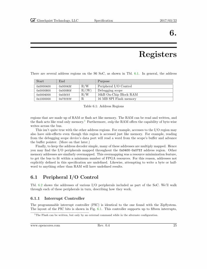
There are several address regions on the S6 SoC, as shown in Tbl. 6.1. In general, the address
Start End Purpose
0x0000400 0x00043f R/W Peripheral I/O Control0x0000800 0x00080f R/(W) Debugging scope0x0004000 0x03fff R/W 16kB On-Chip Block RAM0x1000000 0x7fffff R 16 MB SPI Flash memory
Table 6.1: Address Regions
regions that are made up of RAM or flash act like memory. The RAM can be read and written, andthe flash acts like read only memory.1 Furthermore, only the RAM offers the capability of byte-wisewrites across the bus.
This isn’t quite true with the other address regions. For example, accesses to the I/O region mayalso have side-effects–even though this region is accessed just like memory. For example, readingfrom the debugging scope device’s data port will read a word from the scope’s buffer and advancethe buffer pointer. (More on that later.)
Finally, to keep the address decoder simple, many of these addresses are multiply mapped. Henceyou may find the I/O peripherals mapped throughout the 0x0400–0x07ff address region. Othermemory addresses are similarly overmapped. This overmapping was a resource minimization feature,to get the bus to fit within a minimum number of FPGA resources. For this reason, addresses notexplicitly defined in this specification are undefined. Likewise, attempting to write a byte or half-word to anything other than RAM will have undefined results.
6.1 Peripheral I/O Control
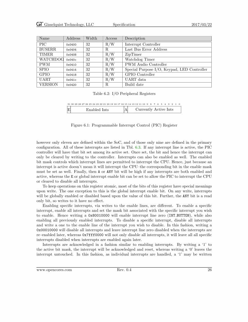
Tbl. 6.2 shows the addresses of various I/O peripherals included as part of the SoC. We’ll walkthrough each of these peripherals in turn, describing how they work.
6.1.1 Interrupt Controller
The programmable interrupt controller (PIC) is identical to the one found with the ZipSystem.The layout of the PIC bits is shown in Fig. 6.1. This controller supports up to fifteen interrupts,
1The Flash can be written, but only by an external command while in the alternate configuration.
www.opencores.com Rev. 0.4 25
Gisselquist Technology, LLC Specification 2017/03/22
Name Address Width Access Description
PIC 0x0400 32 R/W Interrupt ControllerBUSERR 0x0404 32 R Last Bus Error AddressTIMER 0x0408 32 R/W ZipTimerWATCHDOG 0x040c 32 R/W Watchdog TimerPWM 0x0410 32 R/W PWM Audio ControllerSPIO 0x0414 32 R/W Special Purpose I/O, Keypad, LED ControllerGPIO 0x0418 32 R/W GPIO ControllerUART 0x041c 32 R/W UART dataVERSION 0x0420 32 R Build date
Table 6.2: I/O Peripheral Registers
012345678910111213141516171819202122232425262728293031
E Enabled Ints A Currently Active Ints
Figure 6.1: Programmable Interrupt Control (PIC) Register
however only eleven are defined within the SoC, and of those only nine are defined in the primaryconfiguration. All of these interrupts are listed in Tbl. 6.3. If any interrupt line is active, the PICcontroller will have that bit set among its active set. Once set, the bit and hence the interrupt canonly be cleared by writing to the controller. Interrupts can also be enabled as well. The enabledbit mask controls which interrupt lines are permitted to interrupt the CPU. Hence, just because aninterrupt is active doesn’t mean it will interrupt the CPU–the corresponding bit in the enable maskmust be set as well. Finally, then A or ANY bit will be high if any interrupts are both enabled andactive, whereas the E or global interrupt enable bit can be set to allow the PIC to interrupt the CPUor cleared to disable all interrupts.
To keep operations on this register atomic, most of the bits of this register have special meaningsupon write. The one exception to this is the global interrupt enable bit. On any write, interruptswill be globally enabled or disabled based upon the value of this bit. Further, the ANY bit is a readonly bit, so writes to it have no effect.
Enabling specific interrupts, via writes to the enable lines, are different. To enable a specificinterrupt, enable all interrupts and set the mask bit associated with the specific interrupt you wishto enable. Hence writing a 0x80010000 will enable interrupt line zero (INT BUTTON), while alsoenabling all previously enabled interrupts. To disable a specific interrupt, disable all interruptsand write a one to the enable line of the interrupt you wish to disable. In this fashion, writing a0x00010000 will disable all interrupts and leave interrupt line zero disabled when the interrupts arere–enabled later, whereas 0x7fff0000 will not only disable all interrupts, it will leave all all specificinterrupts disabled when interrupts are enabled again later.
Interrupts are acknowledged in a fashion similar to enabling interrupts. By writing a ‘1’ tothe active bit mask, the interrupt will be acknowledged and reset, whereas writing a ‘0’ leaves theinterrupt untouched. In this fashion, as individual interrupts are handled, a ‘1’ may be written
www.opencores.com Rev. 0.4 26
Gisselquist Technology, LLC Specification 2017/03/22
Name Bit Mask Description
INT BUTTON 0x001 A Button has been pressed.INT BUSERR 0x002 A Wishbone bus error has taken placeINT SCOPE 0x004 The Scope has completed its collectionINT TIMER 0x010 Timer-A has reached zeroINT TIMB 0x020 Timer-B has reached zero. (Alternate config only.)INT UARTRX 0x040 A character has been received via the UARTINT UARTTX 0x080 The transmit UART is idle, and ready for its next character.INT KEYPAD 0x100 One of the keypad wires has been pulled low.INT AUDIO 0x200 The audio device is ready for its next sampleINT GPIO 0x400 The GPIO input lines have changed values.INT FLASH 0x800 The flash device has finished either its erase or write cycle, and
is ready for its next command. (Alternate config only.)
Table 6.3: Hardware Interrupts
to this bottom mask to clear the interrupt. Be aware, however, that any write for the purpose ofacknowledging an interrupt will also globally enable or disable interrupts.
6.1.2 Last Bus Error Address
The Bus Error peripheral simply records the address of the last bus error, and sets an interruptupon receiving a bus error. (The interrupt itself is kind of useless ...) The address can be usefulwhen debugging. While the peripheral may only be read, setting it is really as easy as creating abus error and trapping the result. Another use for this is upon any reboot, it is possible to read theaddress of the last bus error and perhaps learn something of what caused the CPU to restart.
6.1.3 ZipTimer
The S6 SoC contains two ZipTimers, one general purpose and one watchdog, available for the CPUto use. These are both countdown timers. Writing any non–zero value to them will cause themto immediately start counting down from that value towards zero, and to interrupt the CPU uponthe transition to zero. Writing a new value while the timer is running will cause that new value toautomatically load into the timer and start counting from there. Writing a zero to the timer disablesthe timer, and causes it to stop.
The general purpose ZipTimer can be set to auto reload by setting the top bit as well as theinterval. When so set, the timer will automatically load it’s last set value upon reaching zero andinterrupting the CPU. This effectively turns it into an interval timer. To set this feature, write tothe timer the number of clock ticks before an interrupt, but also set the high order bit. In thisfashion, writing a 0x8001387f will interrupt the CPU every millisecond, starting one millisecondafter the write takes place (assuming an 80 MHz system clock).2
2Note that, since the timer spends a cycle at zero, setting it for a 80,000 cycle period requires setting the timer
value to one less than 80,000.
www.opencores.com Rev. 0.4 27
Gisselquist Technology, LLC Specification 2017/03/22
012345678910111213141516171819202122232425262728293031
Unused S G E Sample
Figure 6.2: PWM Audio Controller Bitfields
The watchdog timer has been wired for a different purpose. It does not support auto reload, norwill it interrupt the CPU. When this timer transitions to zero, the CPU will be rebooted. One wayto use this timer would be in conjunction with the general purpose timer, and to write a number toit upon any entry to the interrupt service routine. If given enough time, this would cause the CPUto reboot if for any reason it locked up and failed to interrupt at the general timer interrupt requesttime.
The ZipOS uses the ZipTimer for task swapping. By setting the timer for 1 ms, the ZipOSexamines every task for a potential task swap every millisecond. Of course, if the various tasks arerunning from Flash at 17 clocks per instruction, this means that as few as 4,705 instructions maybe executed between timer interrupts, but this can be tuned if necessary for better performance.
6.1.4 PWM Audio Controller
The bit fields of the PWM Audio controller are shown in Fig. 6.2. This controller has been designedfor easy writing. To send a sample to the PWM audio controller, simply write the sample to thecontroller and clear the PWM audio interrupt—in that order. When the audio controller interruptsthe CPU again, it is ready for the next sample. Do note, however, that the audio interrupt can onlybe cleared once a new sample has been written to it. Attempts to clear it prior to that will have noeffect. (This is why the order matters.)
The audio sample rate has been fixed at 8 kHz. This rate may be easily changed withinbusmaster.v by simply setting the number of clocks between samples (currently set to 10,000)and rebuilding the primary configuration. Whether or not the CPU can keep up with a higher ratemight be application dependent.
The audio controller supports two additional functionalities, however. The first is that the E bitwill be set upon any read when or if the audio controller is ready for another sample and the Audiointerrupt has been asserted. By polling this bit, for example, the audio driver can be run withoutusing the interrupt functionality.
The second functionality has to do with the two auxiliary control bits present in the PModAMP2audio device. These are the gain and shutdown bits. To set these bits, write a sample to the controllerwhile also setting the E bit. When the E bit is set upon any write, the shutdown and gain bits willalso be set. (Be aware, the shutdown bit is negative logic.) Hence, one may start this interface bywriting a 0x0310000 to the device, and later shut it back off by writing a 0x010000.
6.1.5 Special Purpose I/O
Register SPIO, as shown in Fig. 6.3, is a Special Purpose Input/Output (SPIO) register. It isdesigned to control the on-board LED’s, buttons, and keypad. Upon any read, the register readsthe current state of the keypad column output, the keypad row input, the buttons and the LED’s.Writing is more difficult, in order to make certain that parts of these registers can be modified
www.opencores.com Rev. 0.4 28
Gisselquist Technology, LLC Specification 2017/03/22
012345678910111213141516171819202122232425262728293031
Zeros Kpad Kpad 00 Btn LED
Col OutRow InRead
{
Ignored Col Col LED LED
Out Enable EnableWrite
{
Figure 6.3: SPIO Control Register
012345678910111213141516171819202122232425262728293031
Current Input Vals (x16) Current Output
Output Change Enable Values (16-outs)
Figure 6.4: GPIO Control Register
atomically. Specifically, to change an LED, write the new value as well as a ‘1’ to the correspondingLED change enable bit. The same goes for the keypad column output, a ‘1’ needs to be written tothe corresponding change enable bit in order for a new value to be accepted.
As examples, writing a 0x0ff to the SPIO register will turn all LED’s on, 0x0f0 will turn allLED’s off, and 0x011 and 0x010 will turn LED0 on and then off again respectively.
The keypad is a little bit tricker. To wait for a keypad interrupt, one needs to set the columnoutputs to zero. To do this, write a 0x0f00 to the SPIO register. When a user then presses a key,one of the row inputs will go low and an interrupt will be asserted. The key must then be debouncedin software. The ZipOS accomplishes this by waiting for 5ms. Once debounced, the key may beread. To do this, set half of the columns to zero, such as by writing a 0x0cf00 to the SPIO register.If one of the row values is still zero, then one of the two columns tested corresponded with the key.This can then be repeated until the correct column has been determined, at which point the rowcan be read and the key known.
All of this functionality may be checked and tested by loading the alternate configuration andeither reading, wbregs spio, or writing wbregs spio <value>.
The controller will generate a keypad interrupt whenever any row input is zero, and a buttoninterrupt whenever any button value is a one. This is a level triggered interrupt, not edge triggered.What that means is that, once generated, the interrupt will need to be disabled until the key orbutton is released—there will be no interrupt for the release, that part will need to be done insoftware.
6.1.6 General Purpose I/O
The General Purpose Input and Output (GPIO) control register, shown in Fig. 6.4, is quite simpleto use: when read, the top 16–bits indicate the value of the 16–input GPIO pins, whereas the bottom16–bits indicate the value being placed on the 16–output GPIO pins. To change a GPIO pin, writethe new pin’s value to this register, together with setting the corresponding pin in the bit-mask
www.opencores.com Rev. 0.4 29
Gisselquist Technology, LLC Specification 2017/03/22
represented by the upper 16–bits. For example, to set output pin zero, write a 0x010001 to theGPIO device. To clear output pin zero, write a 0x010000. Likewise pin one may be set by writinga 0x020002, and both pins may be set by writing 0x030003, etc. This makes it possible to adjustsome output pins independent of the others.
The GPIO controller, like the keypad or SPIO controller, will also generate an interrupt. TheGPIO interrupt is generated whenever a GPIO input line changes. The interrupt is not selective: ifany line changes, a GPIO interrupt will be generated. There are no “do not care” lines (althoughthe GPIO controller could be easily adjusted to make such “do-not-care” lines if necessary . . . ).
Of the 16 GPIO inputs and the 16 GPIO outputs, two lines have been taken for I2C support, anda third has been stolen to make the PMod’s fit on the board. GPIO line zero, for both input andoutput, is an I2C data line, io sda, and GPIO line one is an I2C clock line, io scl. If the output ofeither of these lines is set to zero, the GPIO controller will pull the line low. Otherwise, the line ispulled up so that other devices may pull it low. If either line is low, when the output control bit ishigh, it is an indicator that another device is sending data across these wires. Likewise GPIO inputline 15 has been fixed to ground in order to support placing the keypad next to the S6 SoC.
6.1.7 UART Data Register
Moving on to the UART . . . although the UART module itself within the S6 SoC is highly config-urable, as built the UART can only handle 9600 Baud, 8–data bits, no parity, and one stop bit.Changing this involves changing the constant UART SETUP within toplevel.v. Further, the UARThas only a single byte data buffer, so reading from the port has a real–time requirement associatedwith it: the data buffer must be emptied before the next value is read. Attempts to read from thisport will either return an 8–bit data value from the port, or if no values are available it will returnan 0x0100 indicating that fact. In general, reading from the UART port involves first waiting forthe interrupt to be ready, second reading from the port itself, and then third immediately clearingthe interrupt. (The interrupt cannot be cleared while data is waiting.) Writing to the UART port isdone in a similar fashion. First, wait until the UART transmit interrupt is asserted (this will likelybe most of the time), second, write to the UART port, and then third, clear the interrupt. As withthe read interrupt, clearing the transmit interrupt prior to writing to the port will have no effect.Likewise, clearing the transmit interrupt after the byte has been written will have no affect either.
6.2 Debugging Scope
The debugging scope consists of two registers, a control register and a data register. It needs to beinternally wired to 32–wires, internal to the S6 SoC, that will be of interest when debugging. Forfurther details on how to configure and use this scope, please see the WBSCOPE project on OpenCores.
6.3 On-Chip Block RAM
The block RAM is the fastest memory available to the processor. It is also the only writable memoryavailable to the processor. Hence all non-constant program data must be placed into block RAM.The ZipCPU can also run instructions from the block RAM if extra speed is desired. When runningfrom block RAM, the ZipCPU will nominally take 6 clocks per instruction, for an effective rate of13 MIPS. Loads or stores to block RAM will take one clock longer.
www.opencores.com Rev. 0.4 30
Gisselquist Technology, LLC Specification 2017/03/22
6.4 Flash Memory
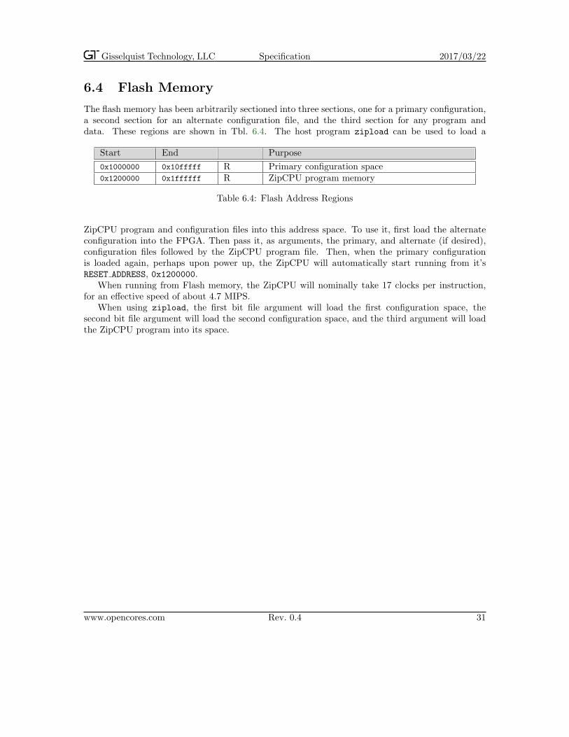
The flash memory has been arbitrarily sectioned into three sections, one for a primary configuration,a second section for an alternate configuration file, and the third section for any program anddata. These regions are shown in Tbl. 6.4. The host program zipload can be used to load a
Start End Purpose
0x1000000 0x10fffff R Primary configuration space0x1200000 0x1ffffff R ZipCPU program memory
Table 6.4: Flash Address Regions
ZipCPU program and configuration files into this address space. To use it, first load the alternateconfiguration into the FPGA. Then pass it, as arguments, the primary, and alternate (if desired),configuration files followed by the ZipCPU program file. Then, when the primary configurationis loaded again, perhaps upon power up, the ZipCPU will automatically start running from it’sRESET ADDRESS, 0x1200000.
When running from Flash memory, the ZipCPU will nominally take 17 clocks per instruction,for an effective speed of about 4.7 MIPS.
When using zipload, the first bit file argument will load the first configuration space, thesecond bit file argument will load the second configuration space, and the third argument will loadthe ZipCPU program into its space.
www.opencores.com Rev. 0.4 31

Gisselquist Technology, LLC Specification 2017/03/22
7.
Clocks
The S6 SoC is designed to run off of one master clock. This clock is derived from the 8 MHz inputclock on the board, by multiplying it up to 80 MHz. The code for doing this can be found in bothtoplevel.v and alttop.v.
www.opencores.com Rev. 0.4 32
Gisselquist Technology, LLC Specification 2017/03/22
8.
I/O Ports
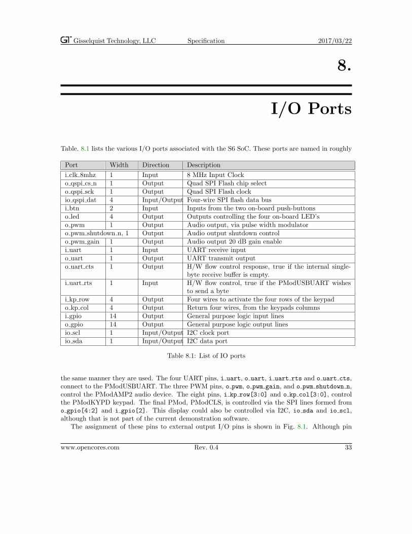
Table. 8.1 lists the various I/O ports associated with the S6 SoC. These ports are named in roughly
Port Width Direction Description
i clk 8mhz 1 Input 8 MHz Input Clocko qspi cs n 1 Output Quad SPI Flash chip selecto qspi sck 1 Output Quad SPI Flash clockio qspi dat 4 Input/Output Four-wire SPI flash data busi btn 2 Input Inputs from the two on-board push-buttonso led 4 Output Outputs controlling the four on-board LED’so pwm 1 Output Audio output, via pulse width modulatoro pwm shutdown n, 1 Output Audio output shutdown controlo pwm gain 1 Output Audio output 20 dB gain enablei uart 1 Input UART receive inputo uart 1 Output UART transmit outputo uart cts 1 Output H/W flow control response, true if the internal single-
byte receive buffer is empty.i uart rts 1 Input H/W flow control, true if the PModUSBUART wishes
to send a bytei kp row 4 Output Four wires to activate the four rows of the keypado kp col 4 Output Return four wires, from the keypads columnsi gpio 14 Output General purpose logic input lineso gpio 14 Output General purpose logic output linesio scl 1 Input/Output I2C clock portio sda 1 Input/Output I2C data port
Table 8.1: List of IO ports
the same manner they are used. The four UART pins, i uart, o uart, i uart rts and o uart cts,connect to the PModUSBUART. The three PWM pins, o pwm, o pwm gain, and o pwm shutdown n,control the PModAMP2 audio device. The eight pins, i kp row[3:0] and o kp col[3:0], controlthe PModKYPD keypad. The final PMod, PModCLS, is controlled via the SPI lines formed fromo gpio[4:2] and i gpio[2]. This display could also be controlled via I2C, io sda and io scl,although that is not part of the current demonstration software.
The assignment of these pins to external output I/O pins is shown in Fig. 8.1. Although pin
www.opencores.com Rev. 0.4 33

Gisselquist Technology, LLC Specification 2017/03/22
Figure 8.1: Physical Locations of Device I/O Ports
www.opencores.com Rev. 0.4 34
Gisselquist Technology, LLC Specification 2017/03/22
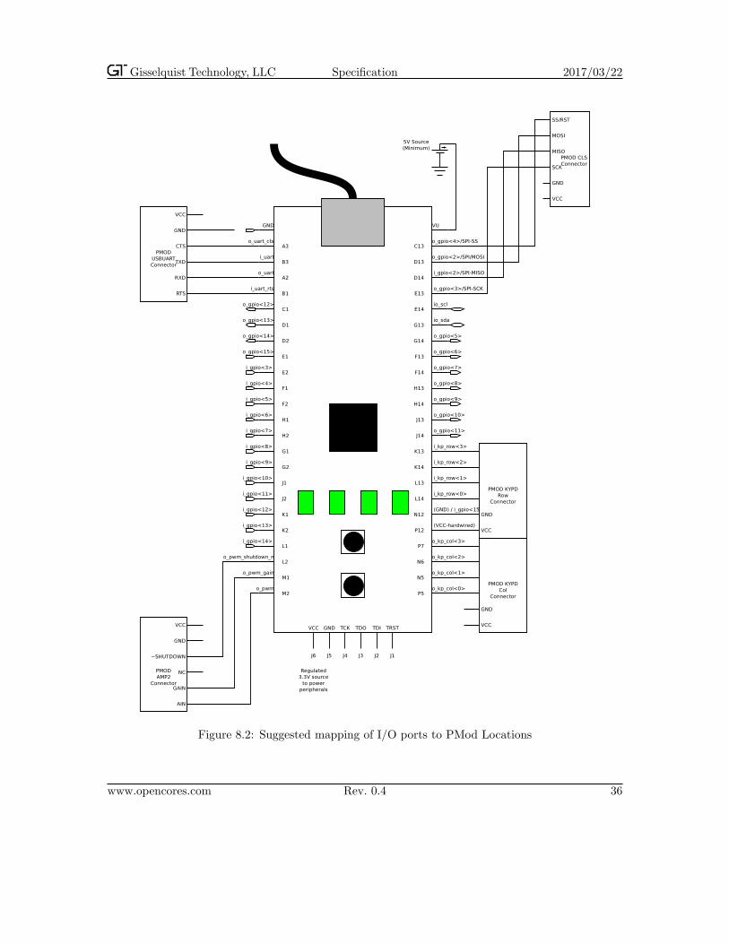
assignment to the actual S6 board has been rather arbitrary, there is a touch of method to themadness. In particular, the S6 SoC pin placement supports placing the PMods in the configurationshown in Fig. 8.2. From this figure you can see that I have tried to minimize the amount of movementnecessary to install any particular PMods, while also making the greatest use of pins on board. Whatmay not be obvious from this picture is that the PMod power and ground lines are all connected topower and ground rails separate from the CMod itself.
As with any piece of open source firmware, these pin assignments are fairly arbitrary and easyto adjust by making changes to the cmod.ucf and cmodtop.ucf files. The main difference betweenthose two files being the DEPP interface supported by alternate configuration, which uses cmod.ucf.
www.opencores.com Rev. 0.4 35
Gisselquist Technology, LLC Specification 2017/03/22
Figure 8.2: Suggested mapping of I/O ports to PMod Locations
www.opencores.com Rev. 0.4 36