Embed Size (px)
Citation preview
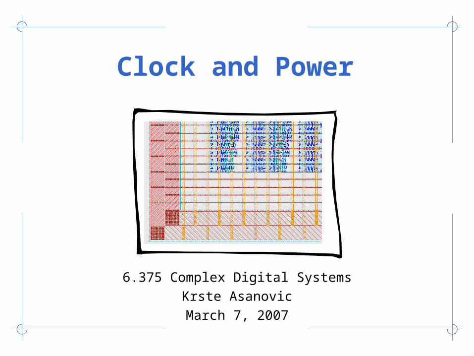
Clock and Power
6.375 Complex Digital Systems
Krste Asanovic
March 7, 2007
6.375 Spring 2007 • L12 Clock and Power • 2
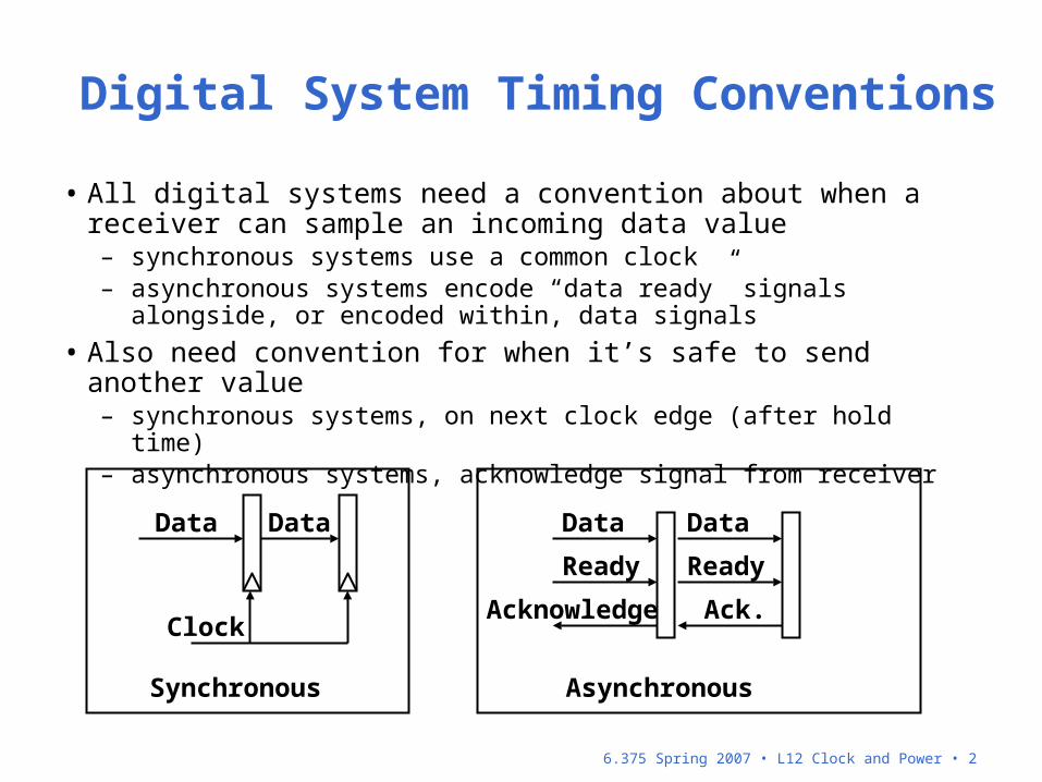
Digital System Timing Conventions
• All digital systems need a convention about when a receiver can sample an incoming data value– synchronous systems use a common clock– asynchronous systems encode “data ready” signals alongside, or
encoded within, data signals
• Also need convention for when it’s safe to send another value– synchronous systems, on next clock edge (after hold time)– asynchronous systems, acknowledge signal from receiver
Data
Clock
Data
Ready
Acknowledge
Synchronous Asynchronous
Data Data
Ready
Ack.
6.375 Spring 2007 • L12 Clock and Power • 3
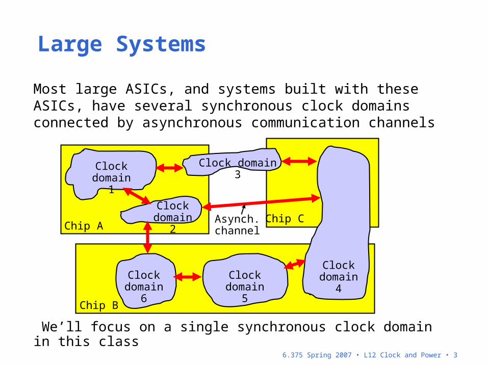
Large Systems
Most large ASICs, and systems built with these ASICs, have several synchronous clock domains connected by asynchronous communication channels
Chip A
Chip B
Chip C
Clock domain 1
Clock domain 4
Clock domain 2
Clock domain 3
Clock domain 5
Clock domain 6
Asynch. channel
We’ll focus on a single synchronous clock domain in this class
6.375 Spring 2007 • L12 Clock and Power • 4
Clock
D QClock
D
Q
Transparent Latched
Clock
D QClock
D
Q
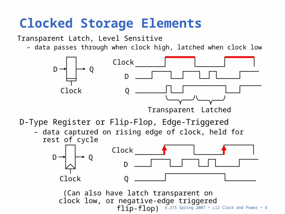
D-Type Register or Flip-Flop, Edge-Triggered– data captured on rising edge of clock, held for rest of cycle
(Can also have latch transparent on clock low, or negative-edge triggered flip-flop)
Clocked Storage ElementsTransparent Latch, Level Sensitive
– data passes through when clock high, latched when clock low
6.375 Spring 2007 • L12 Clock and Power • 5
Flip-Flop Timing Parameters
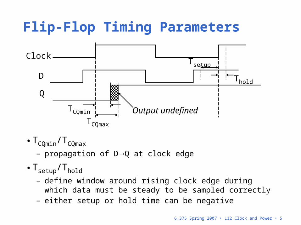
• TCQmin/TCQmax
– propagation of DQ at clock edge
• Tsetup/Thold
– define window around rising clock edge during which data must be steady to be sampled correctly
– either setup or hold time can be negative
Clock
D
Q
TCQmax
TCQmin
Tsetup
Thold
Output undefined
6.375 Spring 2007 • L12 Clock and Power • 6
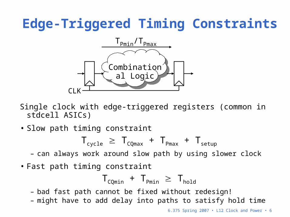
Edge-Triggered Timing Constraints
Single clock with edge-triggered registers (common in stdcell ASICs)
• Slow path timing constraint
Tcycle TCQmax + TPmax + Tsetup
– can always work around slow path by using slower clock
• Fast path timing constraint
TCQmin + TPmin Thold
– bad fast path cannot be fixed without redesign!– might have to add delay into paths to satisfy hold time
CLK
Combinational Logic
TPmin/TPmax
6.375 Spring 2007 • L12 Clock and Power • 7
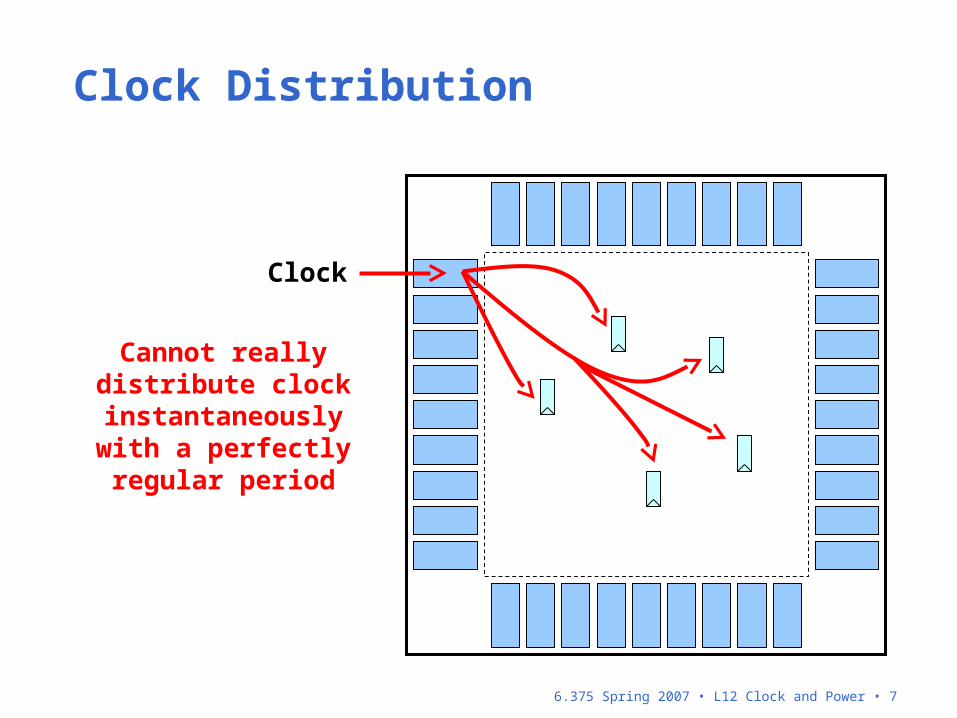
Clock Distribution
Clock
Cannot really distribute clock instantaneouslywith a perfectly regular
period
6.375 Spring 2007 • L12 Clock and Power • 8
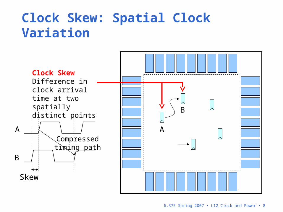
Clock Skew: Spatial Clock Variation
Clock SkewDifference in clock arrival time at two spatially distinct points
A
B
A
B
Skew
Compressed timing path
6.375 Spring 2007 • L12 Clock and Power • 9
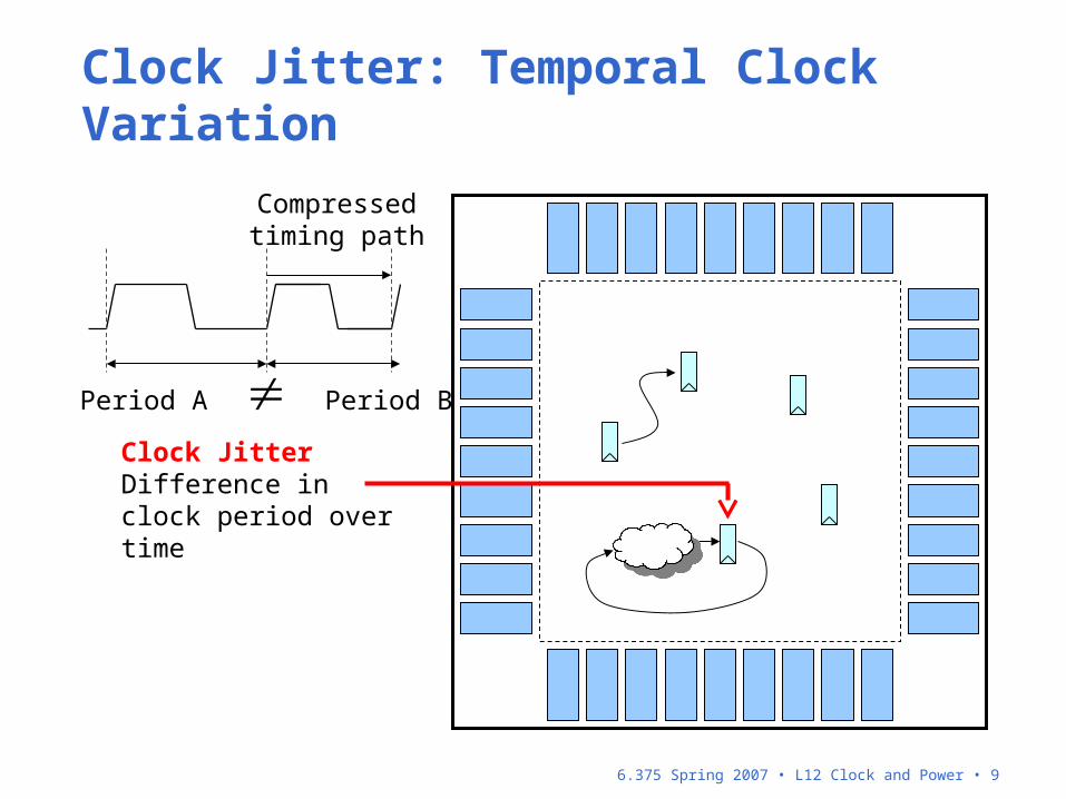
Clock Jitter: Temporal Clock Variation
Clock JitterDifference in clock period over time
Period A Period B
Compressed timing path
6.375 Spring 2007 • L12 Clock and Power • 10
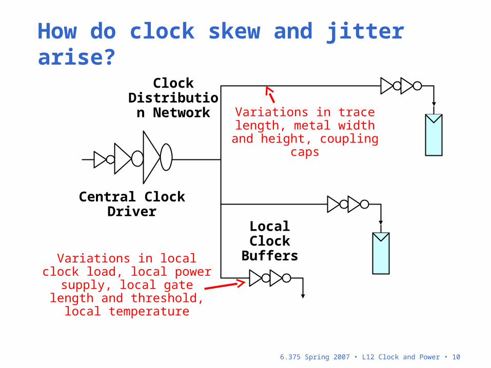
How do clock skew and jitter arise?
Central Clock Driver
Clock Distribution
Network
Local Clock
Buffers
Variations in trace length, metal width and height,
coupling caps
Variations in local clock load, local power supply, local gate
length and threshold, local temperature
6.375 Spring 2007 • L12 Clock and Power • 11
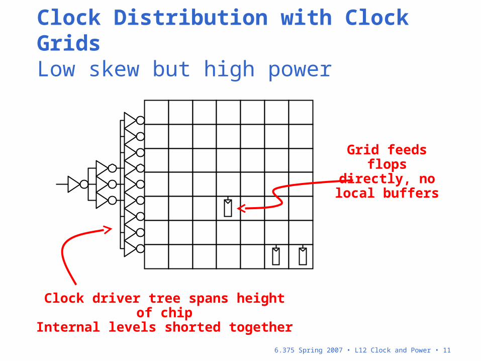
Clock Distribution with Clock GridsLow skew but high power
Clock driver tree spans height of chipInternal levels shorted together
Grid feeds flops directly, no local
buffers
6.375 Spring 2007 • L12 Clock and Power • 12
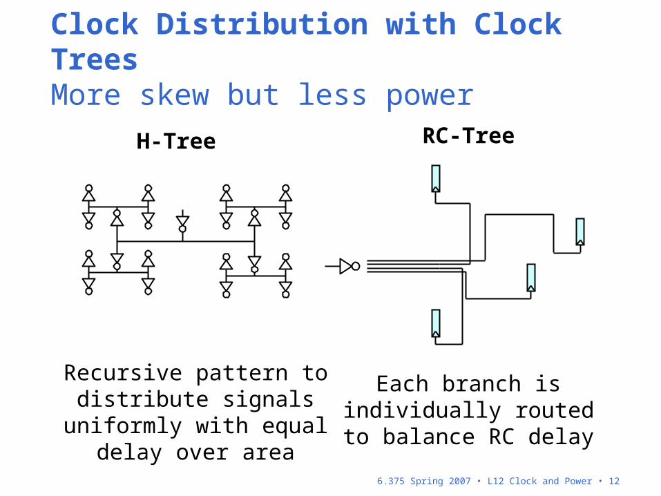
Clock Distribution with Clock TreesMore skew but less power
Recursive pattern to distribute signals uniformly with equal delay over area
Each branch is individually routed to
balance RC delay
H-Tree RC-Tree
6.375 Spring 2007 • L12 Clock and Power • 13
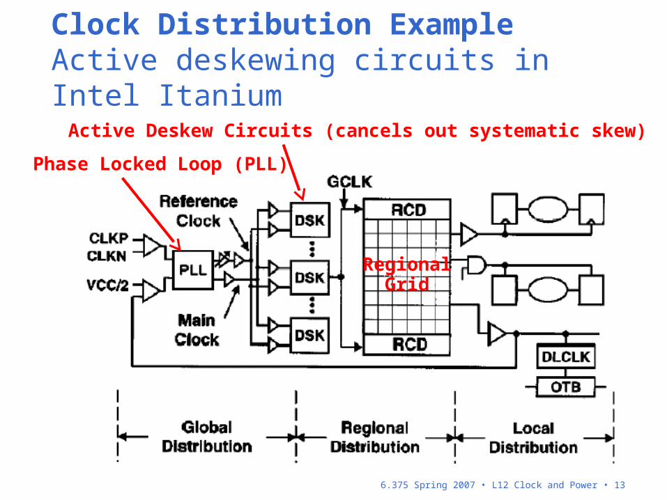
Clock Distribution ExampleActive deskewing circuits in Intel Itanium
Active Deskew Circuits (cancels out systematic skew)
Phase Locked Loop (PLL)
Regional Grid
6.375 Spring 2007 • L12 Clock and Power • 14
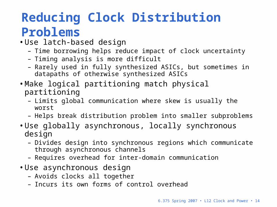
Reducing Clock Distribution Problems• Use latch-based design
– Time borrowing helps reduce impact of clock uncertainty– Timing analysis is more difficult– Rarely used in fully synthesized ASICs, but sometimes in
datapaths of otherwise synthesized ASICs
• Make logical partitioning match physical partitioning– Limits global communication where skew is usually the worst– Helps break distribution problem into smaller subproblems
• Use globally asynchronous, locally synchronous design– Divides design into synchronous regions which communicate
through asynchronous channels– Requires overhead for inter-domain communication
• Use asynchronous design– Avoids clocks all together– Incurs its own forms of control overhead
6.375 Spring 2007 • L12 Clock and Power • 15
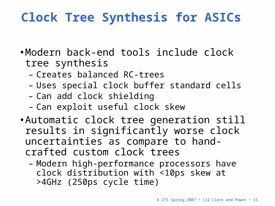
Clock Tree Synthesis for ASICs
• Modern back-end tools include clock tree synthesis– Creates balanced RC-trees– Uses special clock buffer standard cells– Can add clock shielding– Can exploit useful clock skew
• Automatic clock tree generation still results in significantly worse clock uncertainties as compare to hand-crafted custom clock trees– Modern high-performance processors have clock
distribution with <10ps skew at >4GHz (250ps cycle time)
6.375 Spring 2007 • L12 Clock and Power • 16
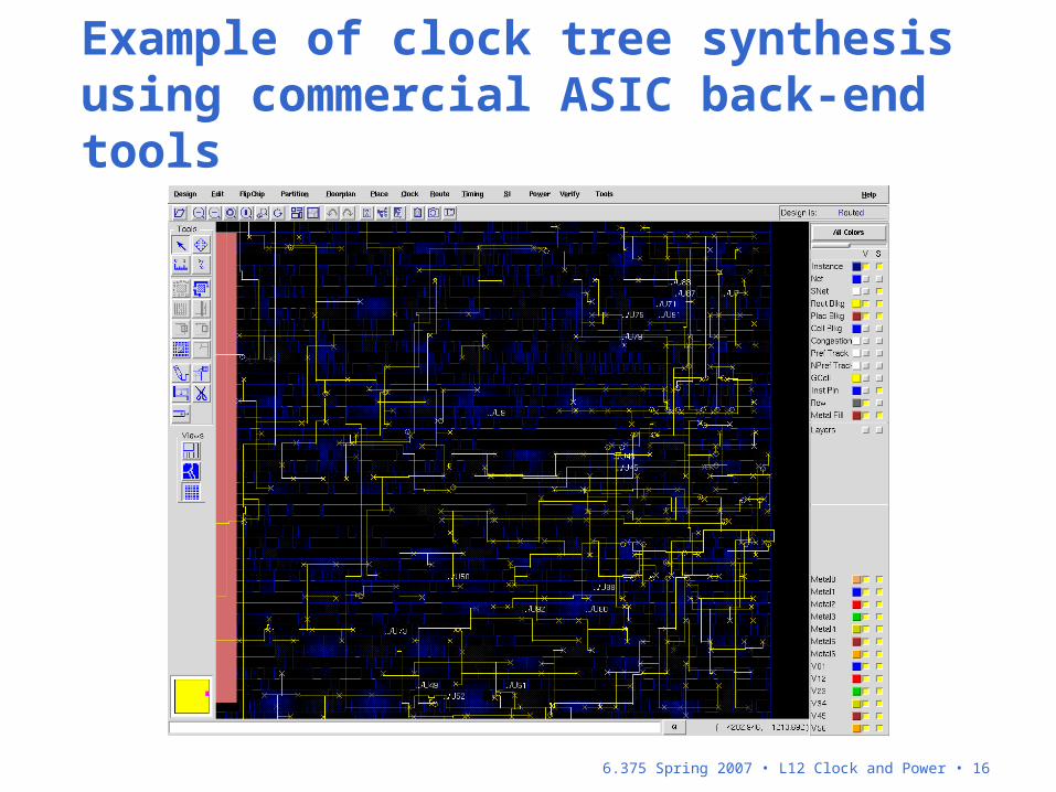
Example of clock tree synthesis using commercial ASIC back-end tools
6.375 Spring 2007 • L12 Clock and Power • 17
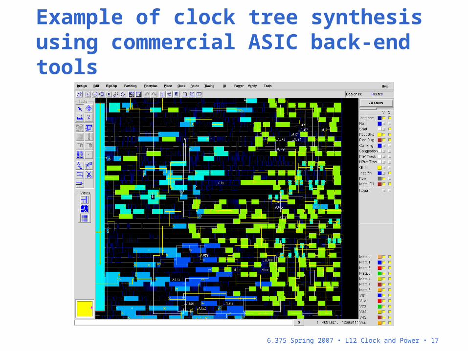
Example of clock tree synthesis using commercial ASIC back-end tools
6.375 Spring 2007 • L12 Clock and Power • 18
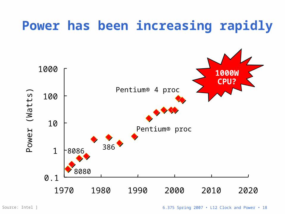
0.1
1
10
100
1000
1970 1980 1990 2000 2010 2020
Pow
er (
Wat
ts)
8080
8086 386
Pentium® proc
Pentium® 4 proc
[ Source: Intel ]
1000W CPU?
Power has been increasing rapidly
6.375 Spring 2007 • L12 Clock and Power • 19
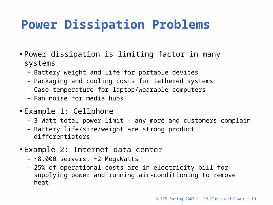
Power Dissipation Problems
• Power dissipation is limiting factor in many systems– Battery weight and life for portable devices– Packaging and cooling costs for tethered systems– Case temperature for laptop/wearable computers– Fan noise for media hubs
• Example 1: Cellphone– 3 Watt total power limit – any more and customers complain– Battery life/size/weight are strong product differentiators
• Example 2: Internet data center– ~8,000 servers, ~2 MegaWatts– 25% of operational costs are in electricity bill for supplying
power and running air-conditioning to remove heat
6.375 Spring 2007 • L12 Clock and Power • 20
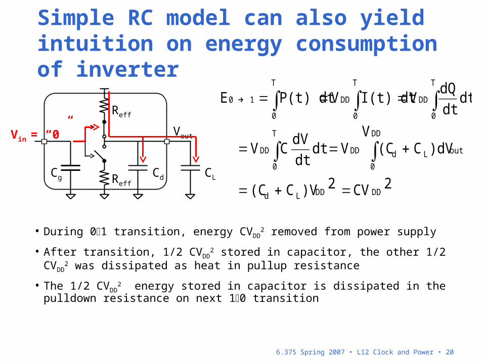
Simple RC model can also yield intuition on energy consumption of inverter
Cg CdReff
Reff
Vout
CL
Vin = “0”
2CV2)VC(C
V)dVC(CVdt
dt
dVCV
dtdt
dQVI(t) dtVP(t) dtE
DDDDLd
DD
0
outLdDD
T
0
DD
T
0
DD
T
0
DD
T
0
10
=+=
+==
===
∫∫
∫∫∫→
• During 01 transition, energy CVDD2 removed from power supply
• After transition, 1/2 CVDD2 stored in capacitor, the other 1/2 CVDD
2 was dissipated as heat in pullup resistance
• The 1/2 CVDD2 energy stored in capacitor is dissipated in the
pulldown resistance on next 10 transition
6.375 Spring 2007 • L12 Clock and Power • 21
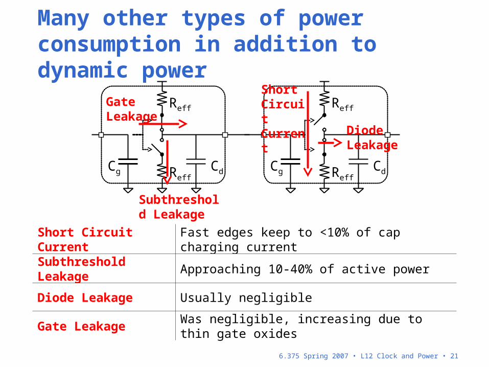
Short Circuit Current Fast edges keep to <10% of cap charging current
Subthreshold Leakage Approaching 10-40% of active power
Diode Leakage Usually negligible
Gate Leakage Was negligible, increasing due to thin gate oxides
Many other types of power consumption in addition to dynamic power
Cg CdReff
Reff
Cg CdReff
Reff
Short Circuit Current
Subthreshold Leakage
Diode Leakage
Gate Leakage
6.375 Spring 2007 • L12 Clock and Power • 22
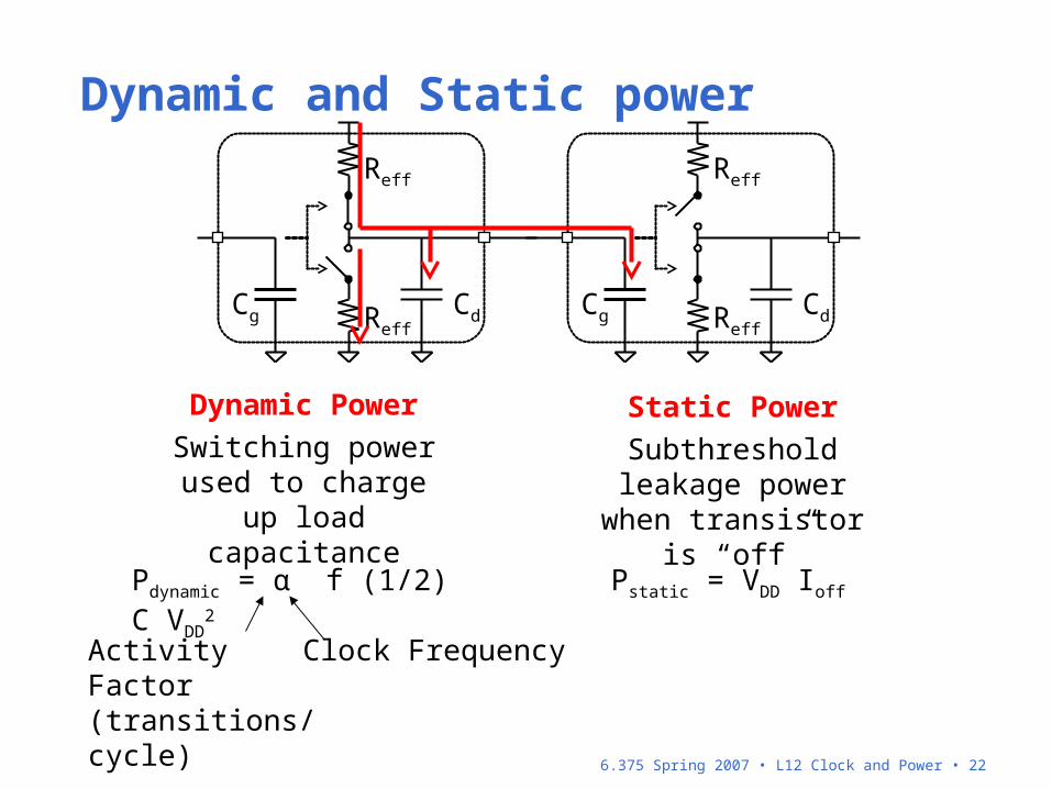
Cg CdReff
Reff
Cg CdReff
Reff
Static Power
Subthreshold leakage power when transistor
is “off”
Pstatic = VDD Ioff
Dynamic Power
Switching power used to charge up load
capacitance
Pdynamic = α f (1/2) C VDD2
Activity Factor (transitions/cycle)
Clock Frequency
Dynamic and Static power
6.375 Spring 2007 • L12 Clock and Power • 23
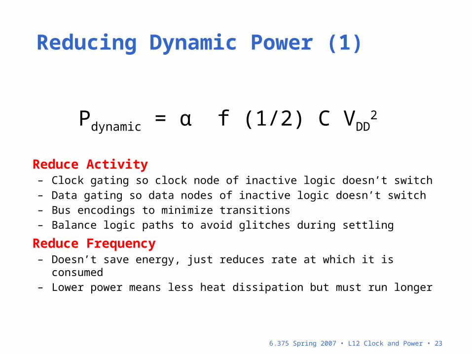
Reducing Dynamic Power (1)
Reduce Activity– Clock gating so clock node of inactive logic doesn’t switch– Data gating so data nodes of inactive logic doesn’t switch– Bus encodings to minimize transitions– Balance logic paths to avoid glitches during settling
Reduce Frequency– Doesn’t save energy, just reduces rate at which it is consumed– Lower power means less heat dissipation but must run longer
Pdynamic = α f (1/2) C VDD2
6.375 Spring 2007 • L12 Clock and Power • 24
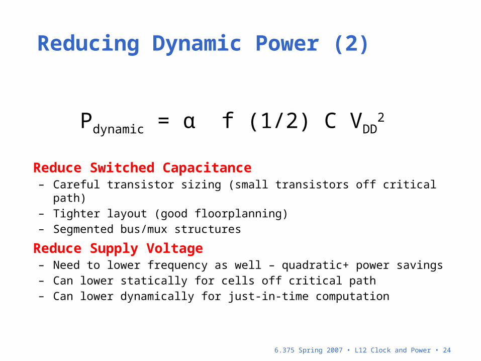
Reducing Dynamic Power (2)
Reduce Switched Capacitance– Careful transistor sizing (small transistors off critical path)– Tighter layout (good floorplanning)– Segmented bus/mux structures
Reduce Supply Voltage– Need to lower frequency as well – quadratic+ power savings– Can lower statically for cells off critical path – Can lower dynamically for just-in-time computation
Pdynamic = α f (1/2) C VDD2
6.375 Spring 2007 • L12 Clock and Power • 25
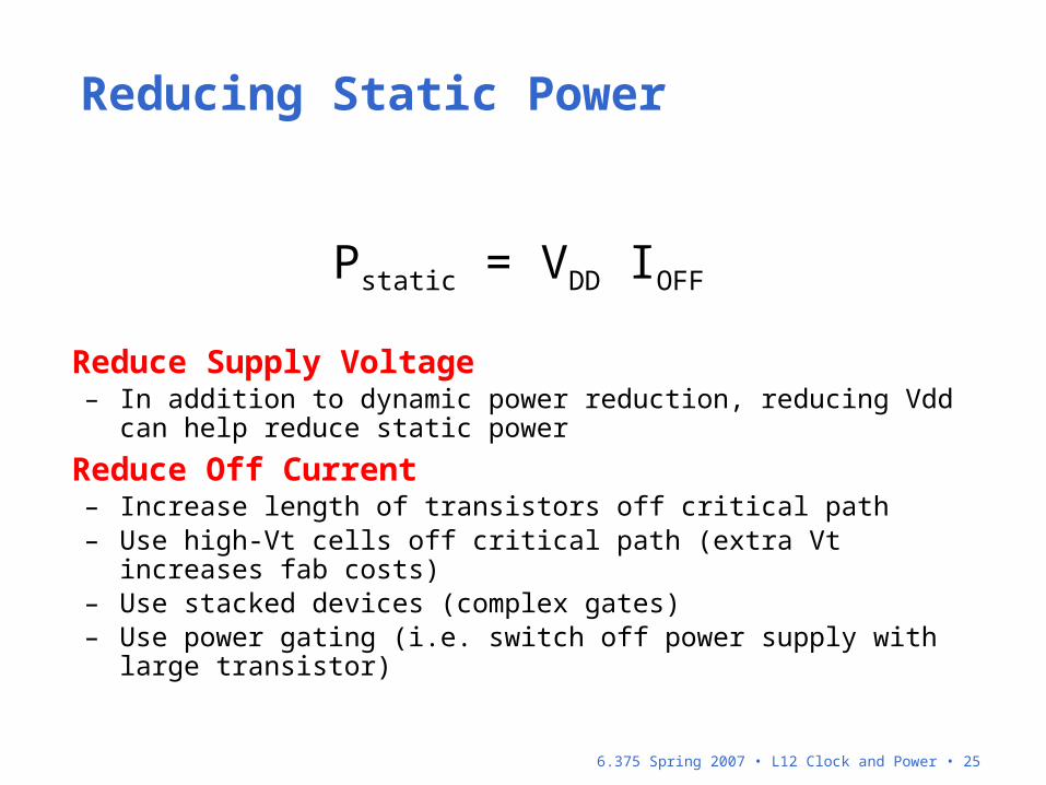
Reducing Static Power
Reduce Supply Voltage– In addition to dynamic power reduction, reducing Vdd can help
reduce static power
Reduce Off Current– Increase length of transistors off critical path– Use high-Vt cells off critical path (extra Vt increases fab costs)– Use stacked devices (complex gates)– Use power gating (i.e. switch off power supply with large transistor)
Pstatic = VDD IOFF
6.375 Spring 2007 • L12 Clock and Power • 26
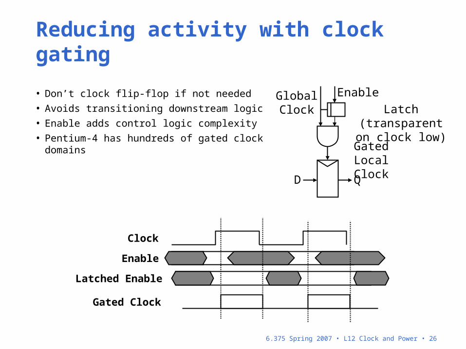
• Don’t clock flip-flop if not needed
• Avoids transitioning downstream logic
• Enable adds control logic complexity
• Pentium-4 has hundreds of gated clock domains
Global Clock
Gated Local Clock
Enable
D Q
Latch (transparent on clock low)
Clock
Enable
Latched Enable
Gated Clock
Reducing activity with clock gating
6.375 Spring 2007 • L12 Clock and Power • 27
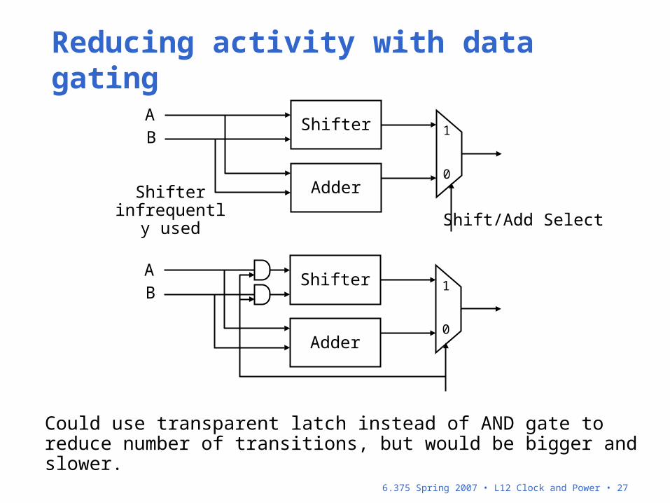
Shifter
Adder
1
0
AB
Shifter infrequently
used Shift/Add Select
Shifter
Adder
1
0
AB
Could use transparent latch instead of AND gate to reduce number of transitions, but would be bigger and slower.
Reducing activity with data gating
6.375 Spring 2007 • L12 Clock and Power • 28
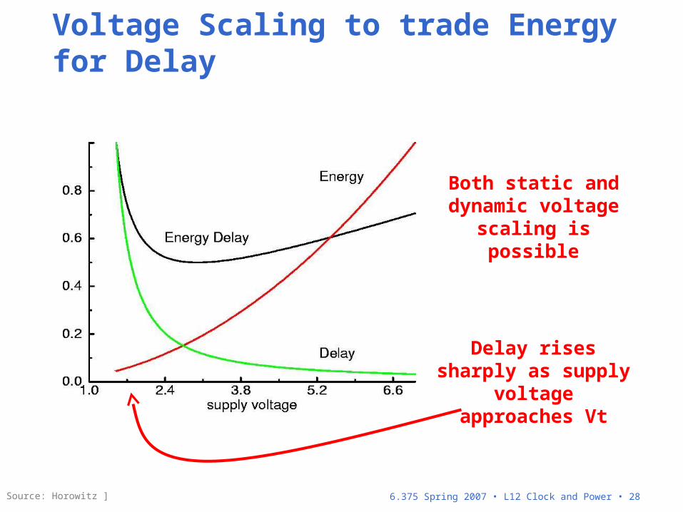
Voltage Scaling to trade Energy for Delay
[ Source: Horowitz ]
Both static and dynamic voltage
scaling is possible
Delay rises sharply as supply voltage
approaches Vt
6.375 Spring 2007 • L12 Clock and Power • 29
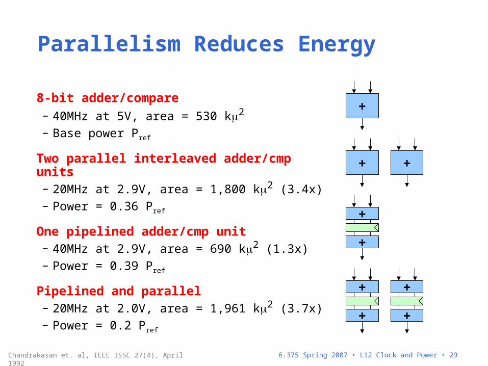
Parallelism Reduces Energy
8-bit adder/compare– 40MHz at 5V, area = 530 k2
– Base power Pref
Two parallel interleaved adder/cmp units– 20MHz at 2.9V, area = 1,800 k2 (3.4x)– Power = 0.36 Pref
One pipelined adder/cmp unit– 40MHz at 2.9V, area = 690 k2 (1.3x)– Power = 0.39 Pref
Pipelined and parallel– 20MHz at 2.0V, area = 1,961 k2 (3.7x)– Power = 0.2 Pref
Chandrakasan et. al, IEEE JSSC 27(4), April 1992
+
+ +
+
+
+
+
+
+
6.375 Spring 2007 • L12 Clock and Power • 30
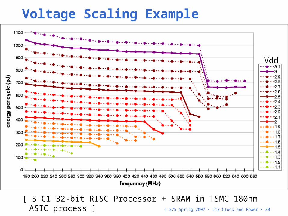
Voltage Scaling Example
[ STC1 32-bit RISC Processor + SRAM in TSMC 180nm ASIC process ]
Vdd
6.375 Spring 2007 • L12 Clock and Power • 31
Reducing Power in ASIC Designs (1)
• Minimize activity– Automatic clock gating is possible if tools can
infer gating from HDL– Partition designs so minimal number of
components activated to perform each operation
• Use lowest voltage and slowest frequency necessary to reach target performance– Use pipelined and parallel architectures if
possible
6.375 Spring 2007 • L12 Clock and Power • 32
Reducing Power in ASIC Designs (2)
• Reducing switched capacitance– Design efficient RTL! Biggest savings come from picking better
hardware algorithms to reduce power and area– Floorplan units to reduce length of power-hungry global wires
• Optimizing for static power– Reduce amount of logic required for function, multiplex units– Partition design such that components can be power-gated or
have independent voltage supplies– Modern standard cell libraries include low-power cells, high-VT
cells, and low-VT cells – tools can automatically replace non-critical cells to optimize for static power
6.375 Spring 2007 • L12 Clock and Power • 33
Power Distribution
6.375 Spring 2007 • L12 Clock and Power • 34
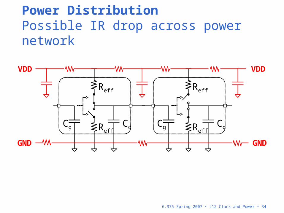
Power DistributionPossible IR drop across power network
Cg CdReff
Reff
Cg CdReff
Reff
VDD VDD
GNDGND
6.375 Spring 2007 • L12 Clock and Power • 35
Cg CdReff
Reff
Cg CdReff
Reff
VDD VDD
GNDGND
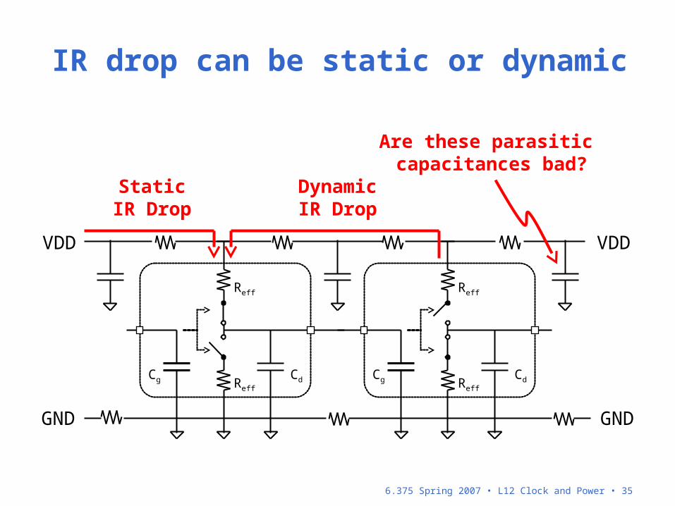
StaticIR Drop
DynamicIR Drop
Are these parasitic capacitances bad?
IR drop can be static or dynamic
6.375 Spring 2007 • L12 Clock and Power • 36
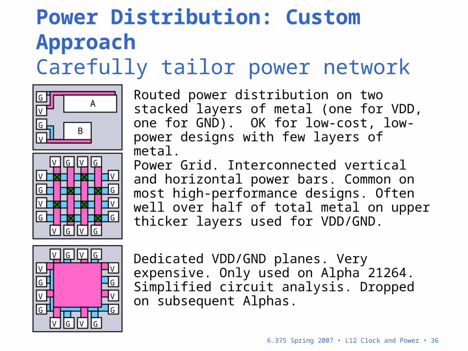
Power Distribution: Custom ApproachCarefully tailor power network
Routed power distribution on two stacked layers of metal (one for VDD, one for GND). OK for low-cost, low-power designs with few layers of metal.
Power Grid. Interconnected vertical and horizontal power bars. Common on most high-performance designs. Often well over half of total metal on upper thicker layers used for VDD/GND.
Dedicated VDD/GND planes. Very expensive. Only used on Alpha 21264. Simplified circuit analysis. Dropped on subsequent Alphas.
A
B
V
V
G
G
G G
V V
G G
V V
V G V G
V G V G
G G
V V
G G
V V
V G V G
V G V G
6.375 Spring 2007 • L12 Clock and Power • 37
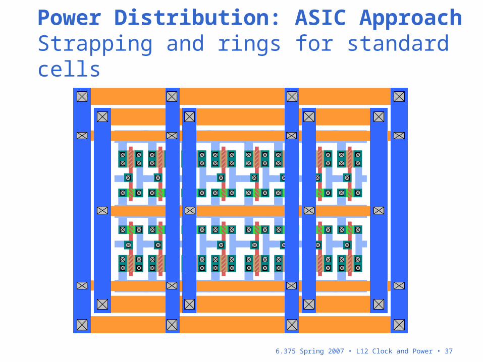
Power Distribution: ASIC ApproachStrapping and rings for standard cells
6.375 Spring 2007 • L12 Clock and Power • 38
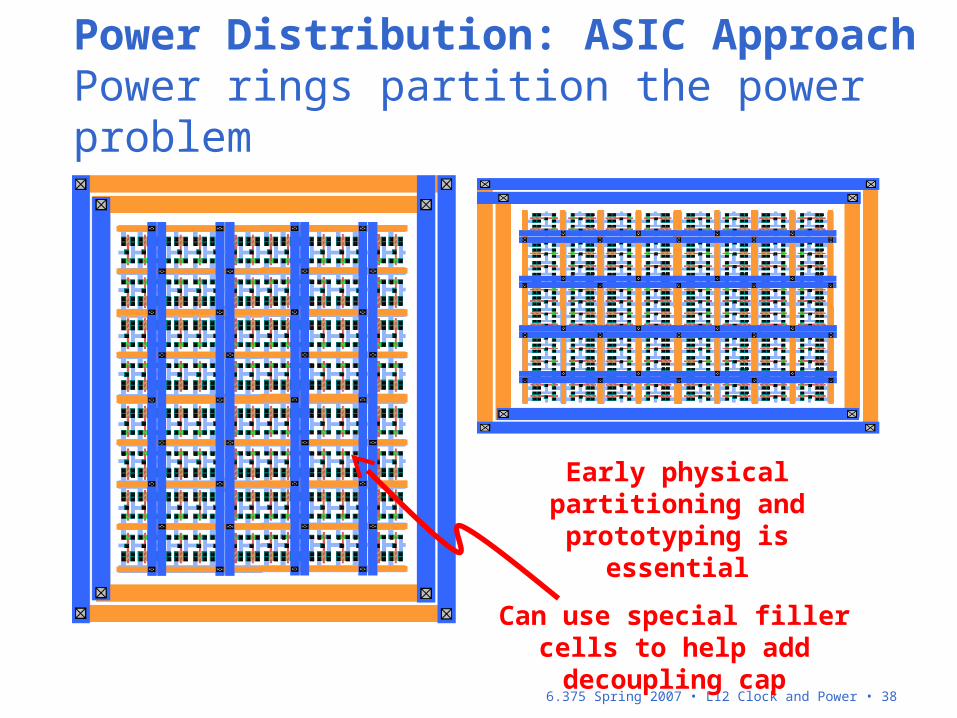
Power Distribution: ASIC ApproachPower rings partition the power problem
Early physical partitioning and prototyping is
essential
Can use special filler cells to help add decoupling cap
6.375 Spring 2007 • L12 Clock and Power • 39
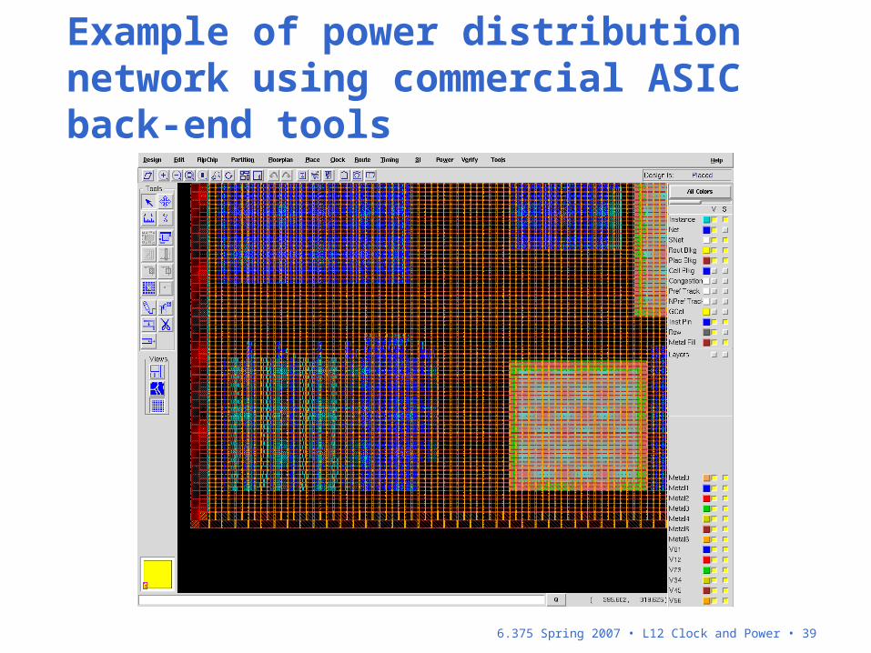
Example of power distribution network using commercial ASIC back-end tools
6.375 Spring 2007 • L12 Clock and Power • 40
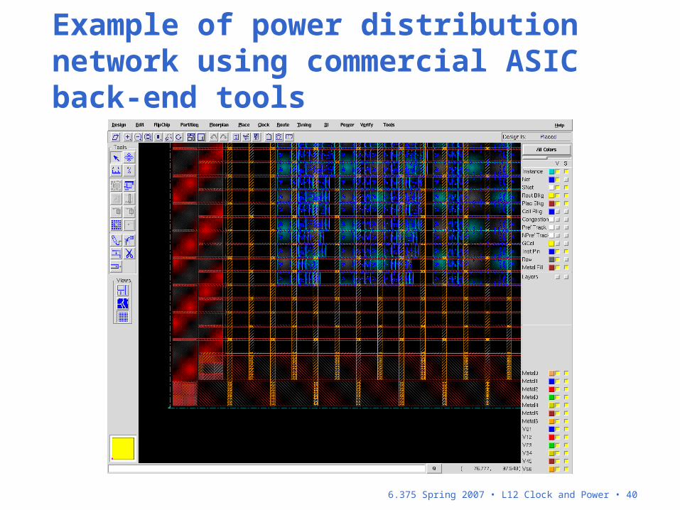
Example of power distribution network using commercial ASIC back-end tools