Embed Size (px)
Citation preview

Click to edit Master title style
Click to edit Master text styles Second Level
Third Level Fourth Level
Fifth Level
Click to edit Master title style
Click to edit Master text styles Second Level Third Level Fourth Level Fifth Level
Katedra Mikroelektroniki i Technik Informatycznych PŁ M. Napieralska
Struktura CMOS
NWELLPWELL
podłoże P
NMOS PMOS
obszary słabo domieszkowanego drenu i źródła
przelotka (VIA)
kontakt
tlenek polowy(utlenianie podłoża)
warstwy izolacyjne(CVD)
metal II metal I

Click to edit Master title style
Click to edit Master text styles Second Level
Third Level Fourth Level
Fifth Level
Click to edit Master title style
Click to edit Master text styles Second Level Third Level Fourth Level Fifth Level
Katedra Mikroelektroniki i Technik Informatycznych PŁ M. Napieralska
p-substrate (bulk)
Gate oxide
n+ n+
Ldrawn
Leffective
Source Drain
Poly gate Metal 1CVD oxide
Ldrawn
Wdrawn
Physical structure Layout representation Schematic representation
S D
G
B

Click to edit Master title style
Click to edit Master text styles Second Level
Third Level Fourth Level
Fifth Level
Click to edit Master title style
Click to edit Master text styles Second Level Third Level Fourth Level Fifth Level
Katedra Mikroelektroniki i Technik Informatycznych PŁ M. Napieralska
Tranzystor MOSpowstaje w układzie scalonym zawsze gdy nastapi przecięcie ścieżki polikrzemowej z warstwą dyfuzji
Drain
GateSource
G
S
D

Click to edit Master title style
Click to edit Master text styles Second Level
Third Level Fourth Level
Fifth Level
Click to edit Master title style
Click to edit Master text styles Second Level Third Level Fourth Level Fifth Level
Katedra Mikroelektroniki i Technik Informatycznych PŁ M. Napieralska
Wytworzone maski stanowią matrycę, która pozwala na powielanie struktury układu na całej powierzchni płytki krzemowej

Click to edit Master title style
Click to edit Master text styles Second Level
Third Level Fourth Level
Fifth Level
Click to edit Master title style
Click to edit Master text styles Second Level Third Level Fourth Level Fifth Level
Katedra Mikroelektroniki i Technik Informatycznych PŁ M. Napieralska
Technologiakrzemowa
Wytwarzanie masek (a,b)Wytwarzanie płytek krzemowych (c,d)Wytwarzanie elementów i połączeń (e)Testowanie ostrzowe (f)Selekcja płytek (g)Cięcie płytki (h)Montaż (i)Testowanie końcowe
a) c)
b) d)
e)
f)
g)
h)
i)

Click to edit Master title style
Click to edit Master text styles Second Level
Third Level Fourth Level
Fifth Level
Click to edit Master title style
Click to edit Master text styles Second Level Third Level Fourth Level Fifth Level
Katedra Mikroelektroniki i Technik Informatycznych PŁ M. Napieralska
Wytwarzanie płytek krzemowych
Wytworzenie krzemu polikrystalicznego Wytworzenie monokryształu krzemu Cięcie Polerowanie mechaniczne i chemiczne Czyszczenie Kontrola Pakowanie i wysyłka
Click to edit Master title style
Click to edit Master text styles Second Level
Third Level Fourth Level
Fifth Level
Click to edit Master title style
Click to edit Master text styles Second Level Third Level Fourth Level Fifth Level
Katedra Mikroelektroniki i Technik Informatycznych PŁ M. Napieralska
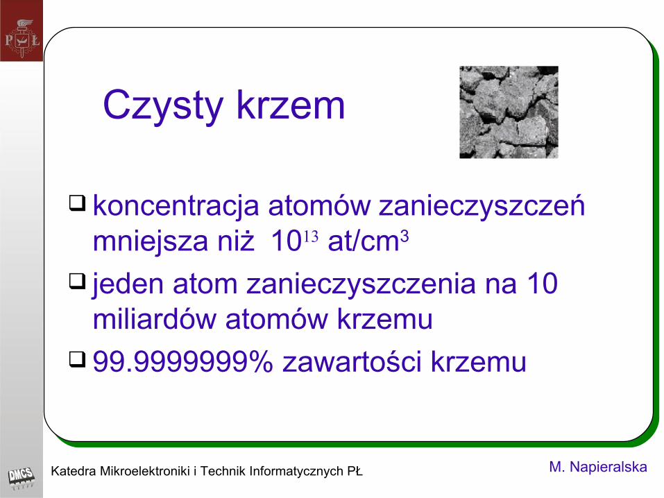
Czysty krzem
koncentracja atomów zanieczyszczeń mniejsza niż 1013 at/cm3
jeden atom zanieczyszczenia na 10 miliardów atomów krzemu
99.9999999% zawartości krzemu
Click to edit Master title style
Click to edit Master text styles Second Level
Third Level Fourth Level
Fifth Level
Click to edit Master title style
Click to edit Master text styles Second Level Third Level Fourth Level Fifth Level
Katedra Mikroelektroniki i Technik Informatycznych PŁ M. Napieralska
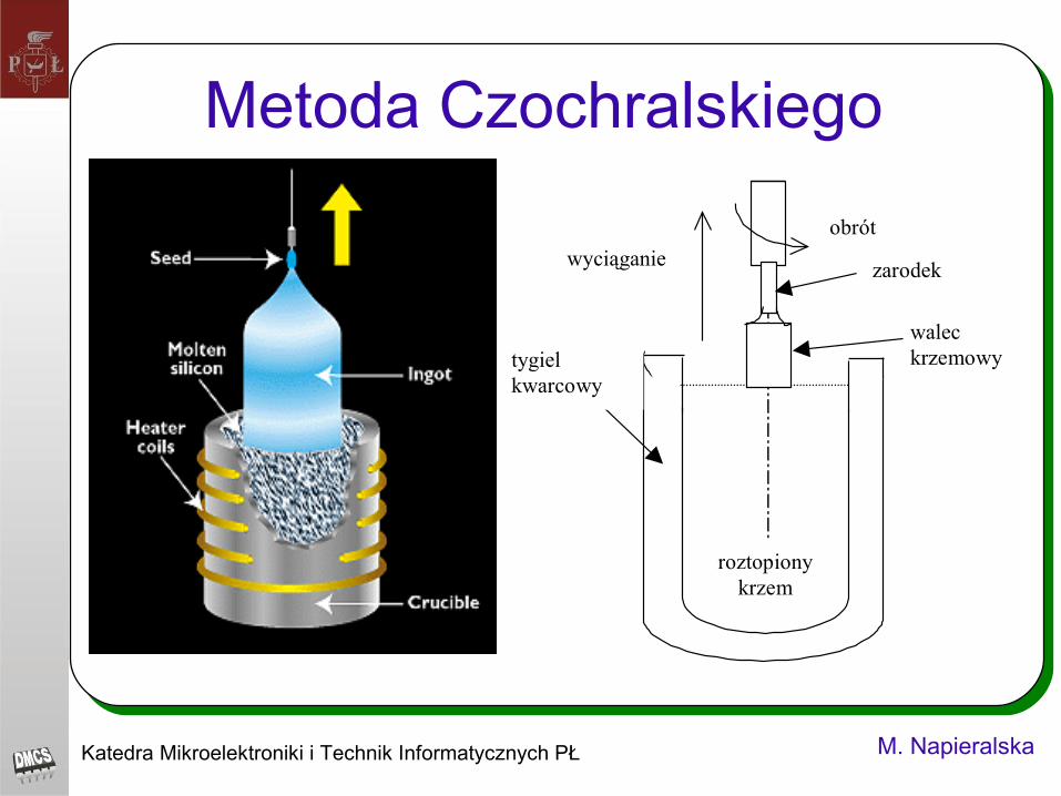
Metoda Czochralskiego
zarodek
obrótwyciąganie
waleckrzemowy
roztopionykrzem
tygielkwarcowy
Click to edit Master title style
Click to edit Master text styles Second Level
Third Level Fourth Level
Fifth Level
Click to edit Master title style
Click to edit Master text styles Second Level Third Level Fourth Level Fifth Level
Katedra Mikroelektroniki i Technik Informatycznych PŁ M. Napieralska
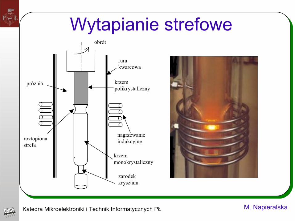
Wytapianie strefoweobrót
rurakwarcowa
nagrzewanieindukcyjneroztopiona
strefa
próżnia
krzemmonokrystaliczny
krzempolikrystaliczny
zarodekkryształu

Click to edit Master title style
Click to edit Master text styles Second Level
Third Level Fourth Level
Fifth Level
Click to edit Master title style
Click to edit Master text styles Second Level Third Level Fourth Level Fifth Level
Katedra Mikroelektroniki i Technik Informatycznych PŁ M. Napieralska
Wytwarzanie elementów i połączeń
Zmiana właściwości materiału lub nałożenie nowej warstwy
Fotolitografia Trawienie
Click to edit Master title style
Click to edit Master text styles Second Level
Third Level Fourth Level
Fifth Level
Click to edit Master title style
Click to edit Master text styles Second Level Third Level Fourth Level Fifth Level
Katedra Mikroelektroniki i Technik Informatycznych PŁ M. Napieralska
Zmiana właściwości materiału
Domieszkowanie w drodze dyfuzji Domieszkowanie przez implantację jonów Utlenianie podłoża
Click to edit Master title style
Click to edit Master text styles Second Level
Third Level Fourth Level
Fifth Level
Click to edit Master title style
Click to edit Master text styles Second Level Third Level Fourth Level Fifth Level
Katedra Mikroelektroniki i Technik Informatycznych PŁ M. Napieralska
Domieszkowanie w drodze dyfuzji
Temperatura 800 - 1200°Cim temperatura jest większa tym dyfuzja jest szybsza
Dyfuzja w ciele stałym jest to ruch atomów w sieci krystalicznej na skutek różnej ich koncentracji w różnych obszarach sieci.

Click to edit Master title style
Click to edit Master text styles Second Level
Third Level Fourth Level
Fifth Level
Click to edit Master title style
Click to edit Master text styles Second Level Third Level Fourth Level Fifth Level
Katedra Mikroelektroniki i Technik Informatycznych PŁ M. Napieralska
Domieszkowanie w drodze dyfuzji
Bor, fosfor lub arsen z fazy gazowej Dyfuzja pionowa i pozioma
p-type epitaxial layer
n-well
Lateraldiffusion
Physical structure cross section Mask (top view)n-well mask
Click to edit Master title style
Click to edit Master text styles Second Level
Third Level Fourth Level
Fifth Level
Click to edit Master title style
Click to edit Master text styles Second Level Third Level Fourth Level Fifth Level
Katedra Mikroelektroniki i Technik Informatycznych PŁ M. Napieralska
Domieszkowanie przez implantację jonów
Jony domieszek rozpędzone w polu elektrycznym Energia jonów: kilkaset keV Wąski profil domieszkowania Uszkodzenie struktury siatki krystalicznej Konieczność wygrzewania Późniejsza dyfuzja domieszek Duża dokładność dawki
Polega na "wbijaniu" przyspieszonych w polu elektrycznymjonów domieszki w materiał podłoża

Click to edit Master title style
Click to edit Master text styles Second Level
Third Level Fourth Level
Fifth Level
Click to edit Master title style
Click to edit Master text styles Second Level Third Level Fourth Level Fifth Level
Katedra Mikroelektroniki i Technik Informatycznych PŁ M. Napieralska
Wytwarzanie warstwy dwutlenku krzemu SiO2
1. Utlenianie • Termiczne w suchym tlenie• Termiczne w parze wodnej

Click to edit Master title style
Click to edit Master text styles Second Level
Third Level Fourth Level
Fifth Level
Click to edit Master title style
Click to edit Master text styles Second Level Third Level Fourth Level Fifth Level
Katedra Mikroelektroniki i Technik Informatycznych PŁ M. Napieralska
Utlenianie podłoża
Temperatura 950 - 1150°C Zużywane podłoże (44% grubości tlenku) Szybkość zależy do ciśnienia i
temperatury Suche lub mokre:
222
22
22 HSiOOHSiSiOOSi
+→+→+

Click to edit Master title style
Click to edit Master text styles Second Level
Third Level Fourth Level
Fifth Level
Click to edit Master title style
Click to edit Master text styles Second Level Third Level Fourth Level Fifth Level
Katedra Mikroelektroniki i Technik Informatycznych PŁ M. Napieralska
2. Nakładanie warstwy tlenku
Tlenki pasywujące i zabezpieczające można otrzymać tylko metodą nakładania
Reakcja chemiczna w atmosferze gazowej

Click to edit Master title style
Click to edit Master text styles Second Level
Third Level Fourth Level
Fifth Level
Click to edit Master title style
Click to edit Master text styles Second Level Third Level Fourth Level Fifth Level
Katedra Mikroelektroniki i Technik Informatycznych PŁ M. Napieralska
Nanoszenie nowych warstw
Chemical Vapor Deposition (CVD) Low Pressure CVD Plasma Enhanced CVD
Physical Vapor Deposition (PVD) Evaporation Sputtering
Metodami osadzania wytwarza się warstwy• dielektryczne,• monokrystaliczne,• polikrystaliczne • warstwy metali trudno topliwych.
Click to edit Master title style
Click to edit Master text styles Second Level
Third Level Fourth Level
Fifth Level
Click to edit Master title style
Click to edit Master text styles Second Level Third Level Fourth Level Fifth Level
Katedra Mikroelektroniki i Technik Informatycznych PŁ M. Napieralska
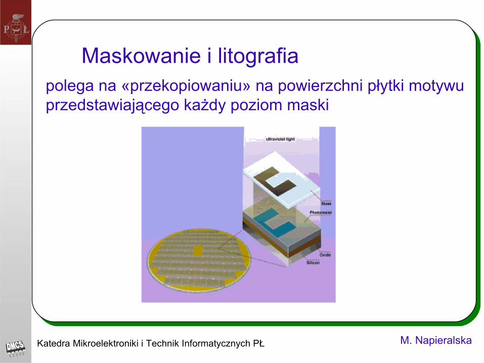
Maskowanie i litografiapolega na «przekopiowaniu» na powierzchni płytki motywuprzedstawiającego każdy poziom maski

Click to edit Master title style
Click to edit Master text styles Second Level
Third Level Fourth Level
Fifth Level
Click to edit Master title style
Click to edit Master text styles Second Level Third Level Fourth Level Fifth Level
Katedra Mikroelektroniki i Technik Informatycznych PŁ M. Napieralska
Fotolitografia (rzeźbienie światłem)
Pokrycie płytki krzemowej równomierną warstwą fotorezystu Naświetlenie Rozpuszczenie obszaru naświetlonego lub nienaświetlonego Operacje technologiczne na
odkrytych obszarach Usunięcie utwardzonego fotorezystu
p
p
p

Click to edit Master title style
Click to edit Master text styles Second Level
Third Level Fourth Level
Fifth Level
Click to edit Master title style
Click to edit Master text styles Second Level Third Level Fourth Level Fifth Level
Katedra Mikroelektroniki i Technik Informatycznych PŁ M. Napieralska
Typy litografii• Optyczna (praktycznie ultrafiolet)
(0.3- 0.4 µm)• Rentgenowska (promienie X o małej energii)
(1- 100 Angstroem) • Elektronowa (strumień elektronów) (dł. fali dla energii
10keV - 1Angstroem)Jonowa (strumień jonów)

Click to edit Master title style
Click to edit Master text styles Second Level
Third Level Fourth Level
Fifth Level
Click to edit Master title style
Click to edit Master text styles Second Level Third Level Fourth Level Fifth Level
Katedra Mikroelektroniki i Technik Informatycznych PŁ M. Napieralska

Click to edit Master title style
Click to edit Master text styles Second Level
Third Level Fourth Level
Fifth Level
Click to edit Master title style
Click to edit Master text styles Second Level Third Level Fourth Level Fifth Level
Katedra Mikroelektroniki i Technik Informatycznych PŁ M. Napieralska
Optical Proximity Correction korekcja gęstości optycznej wiązki
Źródło: Numerical Technologies http://www.numeritech.com

Click to edit Master title style
Click to edit Master text styles Second Level
Third Level Fourth Level
Fifth Level
Click to edit Master title style
Click to edit Master text styles Second Level Third Level Fourth Level Fifth Level
Katedra Mikroelektroniki i Technik Informatycznych PŁ M. Napieralska
Maski wielofazowezwiększanie rozdzielczości odwzorowania cd.
Źródło: Numerical Technologies http://www.numeritech.com
Interferencja światła z sąsiednich otworów Przesunięcie fazowe fali świetlnej
Click to edit Master title style
Click to edit Master text styles Second Level
Third Level Fourth Level
Fifth Level
Click to edit Master title style
Click to edit Master text styles Second Level Third Level Fourth Level Fifth Level
Katedra Mikroelektroniki i Technik Informatycznych PŁ M. Napieralska
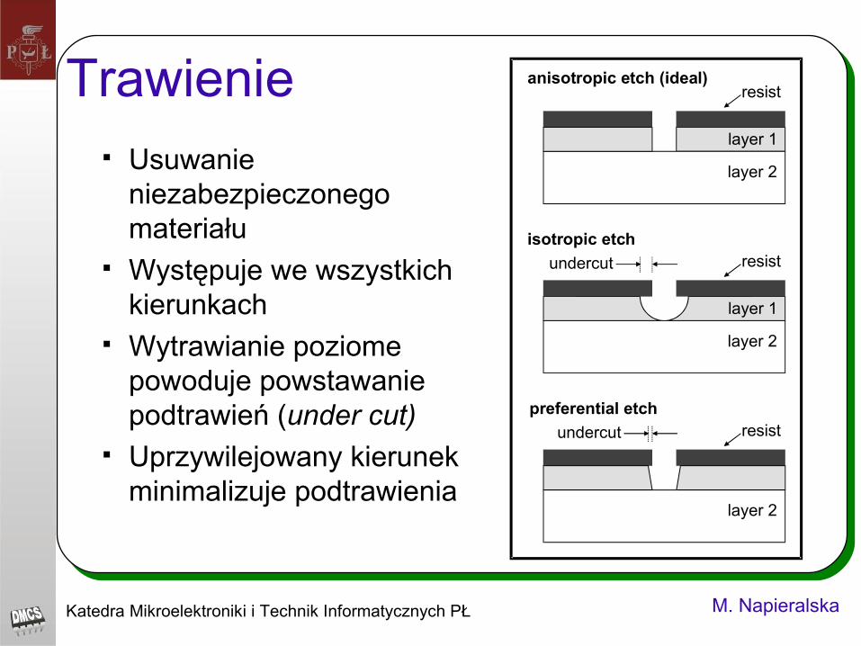
Trawienie anisotropic etch (ideal)resist
layer 1
layer 2
resist
layer 1
layer 2
isotropic etchundercut
resist
layer 1
layer 2
preferential etchundercut
Usuwanie niezabezpieczonego materiału
Występuje we wszystkich kierunkach
Wytrawianie poziome powoduje powstawanie podtrawień (under cut)
Uprzywilejowany kierunek minimalizuje podtrawienia

Click to edit Master title style
Click to edit Master text styles Second Level
Third Level Fourth Level
Fifth Level
Click to edit Master title style
Click to edit Master text styles Second Level Third Level Fourth Level Fifth Level
Katedra Mikroelektroniki i Technik Informatycznych PŁ M. Napieralska
Trawienie - techniki Trawienie mokre – użycie odczynników
chemicznych do usunięcia zbędnego materiału Trawienie suche lub w plazmie użycie
zjonizowanych gazów aktywnych wspomaganych przez wytworzoną plazmą
Zalety trawienia suchego: Wysoka rozdzielczość Wysoka anizotropia

Click to edit Master title style
Click to edit Master text styles Second Level
Third Level Fourth Level
Fifth Level
Click to edit Master title style
Click to edit Master text styles Second Level Third Level Fourth Level Fifth Level
Katedra Mikroelektroniki i Technik Informatycznych PŁ M. Napieralska
Parametry trawieniaselektywność- zdolność do wybiórczego trawienia jednego materiału bez szkody dla innych materiałów znajdujących się na tej samej płytce
anizotropowość - znacznie większa szybkość trawienia w jednym, wyróżnionym kierunku
zapewnia większą wiernośćw odwzorowywaniu kształtów