Embed Size (px)
Citation preview

General DescriptionThe MAX25530 is a highly integrated TFT power supplyand LED backlight driver IC for automotive TFT-LCD ap-plications. The IC integrates one buck-boost converter,one boost converter, two gate-driver supplies, and aboost/SEPIC converter that can power one to four stringsof LEDs in the display backlight.The source-driver power supplies consist of a synchro-nous boost converter and an inverting buck-boost convert-er that can generate voltages up to +18V and down to-7V. The positive source driver can deliver up to 120mA,while the negative source driver is capable of 100mA. Thepositive source-driver supply-regulation voltage (VPOS) isset by connecting an external resistor-divider on FBP orthrough I2C. The negative source-driver supply voltage(VNEG) is always tightly regulated to -VPOS (down to aminimum of -7V). The source-driver supplies operate froman input voltage between 2.8V and 5.5V.The gate-driver power supplies consist of regulatedcharge pumps that generate from +28V to -21.5V and candeliver 10mA or more each depending on the exact con-figuration.The IC features a quad-string LED driver that operatesfrom a separate input voltage (VBATT) and can power upto four strings of LEDs with 150mA (max) of current perstring. The IC features logic-controlled pulse-width-modu-lation (PWM) dimming, with minimum pulse widths as lowas 500ns with the option of phase shifting the LED stringswith respect to one another. When phase shifting is en-abled, each string is turned on at a different time, reducingthe input and output ripple, as well as audible noise. Withphase shifting disabled, the current sinks turn on simulta-neously and parallel connection of current sinks is possi-ble.The startup and shutdown sequences for all power do-mains are controlled using one of the seven preset modes,which are selectable through a resistor on the SEQ pin orthrough the I2C interface.The MAX25530 is available in a 40-pin (6mm x 6mm)TQFN package with an exposed pad, and operates overthe -40°C to +105°C ambient temperature range.
Applications Automotive Dashboards Automotive Central Information Displays Automotive Head Up Displays Automotive Navigation Systems
Benefits and Features 4-Output TFT-LCD Bias Power
• 2.8V to 5.5V Input for the TFT-LCD Section• Integrated 430kHz or 2.2MHz Boost and Buck-
Boost Converters• Positive and Negative 10mA Gate Voltage
Regulators (Tripler/Inverting Doubler) withAdjustable Output Voltage
• Flexible Resistor-Programmable Sequencingthrough the SEQ Pin
• Undervoltage Detection on All Outputs• Low-Quiescent-Current Standby Mode
4-Channel LED Backlight Driver• Up to 150mA Current per Channel• 4.5V to 42V Input Voltage Range• Integrated Boost/SEPIC Controller (440kHz or
2.2MHz)• Dimming Ratio 10,000:1 at 200Hz• Adaptive Voltage Optimization to Reduce Power
Dissipation in the LED Current Sinks• Open-String, Shorted-LED, and Short-to-GND
Diagnostics Low EMI
• Phase-Shift Dimming of LED Strings• Spread Spectrum on LED Driver and TFT• Selectable Switching Frequency
I2C Interface for Control and Diagnostics• Fault Indication through the FLTB pin and I2C• Auto-Retry after Fault Detection
Overload and Thermal Protection -40°C to +105°C Ambient Temperature Operation 40-Pin (6mm x 6mm) TQFN Package with Exposed
Pad AECQ100 Grade 1
Ordering Information appears at end of datasheet.
Click here to ask about the production status of specific part numbers.
MAX25530 Automotive I2C-Controlled 4-Channel 150mABacklight Driver and 4-Output TFT-LCD Bias
19-101001; Rev 0; 2/21
Simplified Block Diagram
MAX25530
BATT
VCC
NDRV
COMP
CS
OVP ISET
DIM
OUT_
LXP
POSITIVE SOFT-START
AND DISCHARGE
HVINP
POS
NEG
INVERTINGREGULATOR
430kHz/2.2MHz
LXN
INN
ENABLE, CONTROL AND FAULT LOGIC
EP
ENDGNDSEQ
400kHz POSITIVE
CHARGE PUMP
400kHz NEGATIVE
CHARGE PUMP DN
DP
PGVDDIN
DGVEE
DGVDDFBPG
FBNG
REF REFERENCE1.25V
LGND1,2
SCL SDA
TFT BOOST CONTROL
430kHz/2.2MHz
I2C
FLTB
GND
NEGATIVE SOFT-START
AND DISCHARGE
ADD
BST
1 of 4 VTHH
VTHL
UP/DOWN COUNTER
+ DAC
gM
CURRENTREF.
DRIVELOGIC
PWMCOMP
5V REGULATOR
+UVLO + BG
VCC
SLOPECOMP 420mV
PHASE-SHIFTLOGIC
TEMP WARNING,
SHUTDOWN
FAULTDETECTION
FBPPGND
1.25V
TEMP WARNING,
SHUTDOWN
MAX25530 Automotive I2C-Controlled 4-Channel 150mABacklight Driver and 4-Output TFT-LCD Bias
www.maximintegrated.com Maxim Integrated | 2
TABLE OF CONTENTSGeneral Description. . . . . . . . . . . . . . . . . . . . . . . . . . . . . . . . . . . . . . . . . . . . . . . . . . . . . . . . . . . . . . . . . . . . . . . . . . . . . . 1Applications . . . . . . . . . . . . . . . . . . . . . . . . . . . . . . . . . . . . . . . . . . . . . . . . . . . . . . . . . . . . . . . . . . . . . . . . . . . . . . . . . . . . 1Benefits and Features . . . . . . . . . . . . . . . . . . . . . . . . . . . . . . . . . . . . . . . . . . . . . . . . . . . . . . . . . . . . . . . . . . . . . . . . . . . . 1Simplified Block Diagram . . . . . . . . . . . . . . . . . . . . . . . . . . . . . . . . . . . . . . . . . . . . . . . . . . . . . . . . . . . . . . . . . . . . . . . . . 2Absolute Maximum Ratings. . . . . . . . . . . . . . . . . . . . . . . . . . . . . . . . . . . . . . . . . . . . . . . . . . . . . . . . . . . . . . . . . . . . . . . . 7Package Information . . . . . . . . . . . . . . . . . . . . . . . . . . . . . . . . . . . . . . . . . . . . . . . . . . . . . . . . . . . . . . . . . . . . . . . . . . . . . 7
40-Pin TQFN . . . . . . . . . . . . . . . . . . . . . . . . . . . . . . . . . . . . . . . . . . . . . . . . . . . . . . . . . . . . . . . . . . . . . . . . . . . . . . . . 7Electrical Characteristics . . . . . . . . . . . . . . . . . . . . . . . . . . . . . . . . . . . . . . . . . . . . . . . . . . . . . . . . . . . . . . . . . . . . . . . . . 7Typical Operating Characteristics . . . . . . . . . . . . . . . . . . . . . . . . . . . . . . . . . . . . . . . . . . . . . . . . . . . . . . . . . . . . . . . . . 16Pin Configuration. . . . . . . . . . . . . . . . . . . . . . . . . . . . . . . . . . . . . . . . . . . . . . . . . . . . . . . . . . . . . . . . . . . . . . . . . . . . . . . 20
MAX25530 . . . . . . . . . . . . . . . . . . . . . . . . . . . . . . . . . . . . . . . . . . . . . . . . . . . . . . . . . . . . . . . . . . . . . . . . . . . . . . . . . 20Pin Description . . . . . . . . . . . . . . . . . . . . . . . . . . . . . . . . . . . . . . . . . . . . . . . . . . . . . . . . . . . . . . . . . . . . . . . . . . . . . . . . 20Functional Diagrams . . . . . . . . . . . . . . . . . . . . . . . . . . . . . . . . . . . . . . . . . . . . . . . . . . . . . . . . . . . . . . . . . . . . . . . . . . . . 23
Detailed Block Diagram . . . . . . . . . . . . . . . . . . . . . . . . . . . . . . . . . . . . . . . . . . . . . . . . . . . . . . . . . . . . . . . . . . . . . . . 23Detailed Description . . . . . . . . . . . . . . . . . . . . . . . . . . . . . . . . . . . . . . . . . . . . . . . . . . . . . . . . . . . . . . . . . . . . . . . . . . . . 24
TFT Power Section. . . . . . . . . . . . . . . . . . . . . . . . . . . . . . . . . . . . . . . . . . . . . . . . . . . . . . . . . . . . . . . . . . . . . . . . . . . 24Source-Driver Power Supplies . . . . . . . . . . . . . . . . . . . . . . . . . . . . . . . . . . . . . . . . . . . . . . . . . . . . . . . . . . . . . . . 24Gate-Driver Power Supplies . . . . . . . . . . . . . . . . . . . . . . . . . . . . . . . . . . . . . . . . . . . . . . . . . . . . . . . . . . . . . . . . . 24Fault Protection . . . . . . . . . . . . . . . . . . . . . . . . . . . . . . . . . . . . . . . . . . . . . . . . . . . . . . . . . . . . . . . . . . . . . . . . . . . 24Output Sequencing Control . . . . . . . . . . . . . . . . . . . . . . . . . . . . . . . . . . . . . . . . . . . . . . . . . . . . . . . . . . . . . . . . . . 25
TFT Sequence with RSEQ = 10k . . . . . . . . . . . . . . . . . . . . . . . . . . . . . . . . . . . . . . . . . . . . . . . . . . . . . . . . . . . 26Description of the LED Driver Section . . . . . . . . . . . . . . . . . . . . . . . . . . . . . . . . . . . . . . . . . . . . . . . . . . . . . . . . . . . . 26
Current-Mode DC-DC Controller . . . . . . . . . . . . . . . . . . . . . . . . . . . . . . . . . . . . . . . . . . . . . . . . . . . . . . . . . . . . . . 278-Bit DAC . . . . . . . . . . . . . . . . . . . . . . . . . . . . . . . . . . . . . . . . . . . . . . . . . . . . . . . . . . . . . . . . . . . . . . . . . . . . . . . 27PWM Dimming . . . . . . . . . . . . . . . . . . . . . . . . . . . . . . . . . . . . . . . . . . . . . . . . . . . . . . . . . . . . . . . . . . . . . . . . . . . 27Low-Dim Mode . . . . . . . . . . . . . . . . . . . . . . . . . . . . . . . . . . . . . . . . . . . . . . . . . . . . . . . . . . . . . . . . . . . . . . . . . . . 28Phase Shifting . . . . . . . . . . . . . . . . . . . . . . . . . . . . . . . . . . . . . . . . . . . . . . . . . . . . . . . . . . . . . . . . . . . . . . . . . . . . 28
Figure 2 Phase-Shifted Outputs . . . . . . . . . . . . . . . . . . . . . . . . . . . . . . . . . . . . . . . . . . . . . . . . . . . . . . . . . . . . 29Undervoltage Lockout . . . . . . . . . . . . . . . . . . . . . . . . . . . . . . . . . . . . . . . . . . . . . . . . . . . . . . . . . . . . . . . . . . . . . . 29Startup Sequence . . . . . . . . . . . . . . . . . . . . . . . . . . . . . . . . . . . . . . . . . . . . . . . . . . . . . . . . . . . . . . . . . . . . . . . . . 29
Stage 1 . . . . . . . . . . . . . . . . . . . . . . . . . . . . . . . . . . . . . . . . . . . . . . . . . . . . . . . . . . . . . . . . . . . . . . . . . . . . . . . 29Stage 2 . . . . . . . . . . . . . . . . . . . . . . . . . . . . . . . . . . . . . . . . . . . . . . . . . . . . . . . . . . . . . . . . . . . . . . . . . . . . . . . 30
Open-LED Management and Overvoltage Protection (OVP) . . . . . . . . . . . . . . . . . . . . . . . . . . . . . . . . . . . . . . . . 30Short-LED Detection . . . . . . . . . . . . . . . . . . . . . . . . . . . . . . . . . . . . . . . . . . . . . . . . . . . . . . . . . . . . . . . . . . . . . . . 31LED Current Control . . . . . . . . . . . . . . . . . . . . . . . . . . . . . . . . . . . . . . . . . . . . . . . . . . . . . . . . . . . . . . . . . . . . . . . 31
FLTB Output . . . . . . . . . . . . . . . . . . . . . . . . . . . . . . . . . . . . . . . . . . . . . . . . . . . . . . . . . . . . . . . . . . . . . . . . . . . . . . . . 31Serial Interface . . . . . . . . . . . . . . . . . . . . . . . . . . . . . . . . . . . . . . . . . . . . . . . . . . . . . . . . . . . . . . . . . . . . . . . . . . . . . . 32
Register Map . . . . . . . . . . . . . . . . . . . . . . . . . . . . . . . . . . . . . . . . . . . . . . . . . . . . . . . . . . . . . . . . . . . . . . . . . . . . . . . . . . 33
MAX25530 Automotive I2C-Controlled 4-Channel 150mABacklight Driver and 4-Output TFT-LCD Bias
www.maximintegrated.com Maxim Integrated | 3
TABLE OF CONTENTS (CONTINUED)Reg Map. . . . . . . . . . . . . . . . . . . . . . . . . . . . . . . . . . . . . . . . . . . . . . . . . . . . . . . . . . . . . . . . . . . . . . . . . . . . . . . . . . . 33Register Details . . . . . . . . . . . . . . . . . . . . . . . . . . . . . . . . . . . . . . . . . . . . . . . . . . . . . . . . . . . . . . . . . . . . . . . . . . . . . 33
Applications Information . . . . . . . . . . . . . . . . . . . . . . . . . . . . . . . . . . . . . . . . . . . . . . . . . . . . . . . . . . . . . . . . . . . . . . . . . 47TFT Power Section. . . . . . . . . . . . . . . . . . . . . . . . . . . . . . . . . . . . . . . . . . . . . . . . . . . . . . . . . . . . . . . . . . . . . . . . . . . 47
Boost Converter . . . . . . . . . . . . . . . . . . . . . . . . . . . . . . . . . . . . . . . . . . . . . . . . . . . . . . . . . . . . . . . . . . . . . . . . . . 47Boost Converter Inductor Selection . . . . . . . . . . . . . . . . . . . . . . . . . . . . . . . . . . . . . . . . . . . . . . . . . . . . . . . . . 47Boost Output-Filter Capacitor Selection . . . . . . . . . . . . . . . . . . . . . . . . . . . . . . . . . . . . . . . . . . . . . . . . . . . . . . 47Setting the POS Voltage . . . . . . . . . . . . . . . . . . . . . . . . . . . . . . . . . . . . . . . . . . . . . . . . . . . . . . . . . . . . . . . . . 47
NEG Inverting Regulator . . . . . . . . . . . . . . . . . . . . . . . . . . . . . . . . . . . . . . . . . . . . . . . . . . . . . . . . . . . . . . . . . . . . 47NEG Regulator Inductor Selection . . . . . . . . . . . . . . . . . . . . . . . . . . . . . . . . . . . . . . . . . . . . . . . . . . . . . . . . . . 47NEG External Diode Selection . . . . . . . . . . . . . . . . . . . . . . . . . . . . . . . . . . . . . . . . . . . . . . . . . . . . . . . . . . . . . 47NEG Output Capacitor Selection . . . . . . . . . . . . . . . . . . . . . . . . . . . . . . . . . . . . . . . . . . . . . . . . . . . . . . . . . . . 47
Setting the DGVDD and DGVEE Output Voltages . . . . . . . . . . . . . . . . . . . . . . . . . . . . . . . . . . . . . . . . . . . . . . . . 48LED Driver Section. . . . . . . . . . . . . . . . . . . . . . . . . . . . . . . . . . . . . . . . . . . . . . . . . . . . . . . . . . . . . . . . . . . . . . . . . . . 48
DC-DC Converter for LED Driver . . . . . . . . . . . . . . . . . . . . . . . . . . . . . . . . . . . . . . . . . . . . . . . . . . . . . . . . . . . . . 48Power-Circuit Design. . . . . . . . . . . . . . . . . . . . . . . . . . . . . . . . . . . . . . . . . . . . . . . . . . . . . . . . . . . . . . . . . . . . . . . 48
Boost Configuration . . . . . . . . . . . . . . . . . . . . . . . . . . . . . . . . . . . . . . . . . . . . . . . . . . . . . . . . . . . . . . . . . . . . . 49SEPIC Configuration . . . . . . . . . . . . . . . . . . . . . . . . . . . . . . . . . . . . . . . . . . . . . . . . . . . . . . . . . . . . . . . . . . . . 49
Current-Sense Resistor and Slope Compensation . . . . . . . . . . . . . . . . . . . . . . . . . . . . . . . . . . . . . . . . . . . . . . . . 50Output Capacitor Selection . . . . . . . . . . . . . . . . . . . . . . . . . . . . . . . . . . . . . . . . . . . . . . . . . . . . . . . . . . . . . . . . . . 51External Switching-MOSFET Selection . . . . . . . . . . . . . . . . . . . . . . . . . . . . . . . . . . . . . . . . . . . . . . . . . . . . . . . . 51Rectifier Diode Selection . . . . . . . . . . . . . . . . . . . . . . . . . . . . . . . . . . . . . . . . . . . . . . . . . . . . . . . . . . . . . . . . . . . . 52Feedback Compensation . . . . . . . . . . . . . . . . . . . . . . . . . . . . . . . . . . . . . . . . . . . . . . . . . . . . . . . . . . . . . . . . . . . 52
Typical Application Circuits . . . . . . . . . . . . . . . . . . . . . . . . . . . . . . . . . . . . . . . . . . . . . . . . . . . . . . . . . . . . . . . . . . . . . . . 54Typical Application Circuit for I2C Mode. . . . . . . . . . . . . . . . . . . . . . . . . . . . . . . . . . . . . . . . . . . . . . . . . . . . . . . . . . . 54Typical Application Circuit for Stand-Alone Mode . . . . . . . . . . . . . . . . . . . . . . . . . . . . . . . . . . . . . . . . . . . . . . . . . . . 55Typical Application Circuit for I2C Mode, SEPIC Topology . . . . . . . . . . . . . . . . . . . . . . . . . . . . . . . . . . . . . . . . . . . . 56
Ordering Information . . . . . . . . . . . . . . . . . . . . . . . . . . . . . . . . . . . . . . . . . . . . . . . . . . . . . . . . . . . . . . . . . . . . . . . . . . . . 57Revision History . . . . . . . . . . . . . . . . . . . . . . . . . . . . . . . . . . . . . . . . . . . . . . . . . . . . . . . . . . . . . . . . . . . . . . . . . . . . . . . 58
MAX25530 Automotive I2C-Controlled 4-Channel 150mABacklight Driver and 4-Output TFT-LCD Bias
www.maximintegrated.com Maxim Integrated | 4

LIST OF FIGURESFigure 1. TFT Sequence with RSEQ = 10kΩ . . . . . . . . . . . . . . . . . . . . . . . . . . . . . . . . . . . . . . . . . . . . . . . . . . . . . . . . . . 26Figure 2. Phase-Shifted Outputs . . . . . . . . . . . . . . . . . . . . . . . . . . . . . . . . . . . . . . . . . . . . . . . . . . . . . . . . . . . . . . . . . . . 29
MAX25530 Automotive I2C-Controlled 4-Channel 150mABacklight Driver and 4-Output TFT-LCD Bias
www.maximintegrated.com Maxim Integrated | 5

LIST OF TABLESTable 1. Sequencing Options . . . . . . . . . . . . . . . . . . . . . . . . . . . . . . . . . . . . . . . . . . . . . . . . . . . . . . . . . . . . . . . . . . . . . 25Table 2. I2C Addresses . . . . . . . . . . . . . . . . . . . . . . . . . . . . . . . . . . . . . . . . . . . . . . . . . . . . . . . . . . . . . . . . . . . . . . . . . . 32
MAX25530 Automotive I2C-Controlled 4-Channel 150mABacklight Driver and 4-Output TFT-LCD Bias
www.maximintegrated.com Maxim Integrated | 6
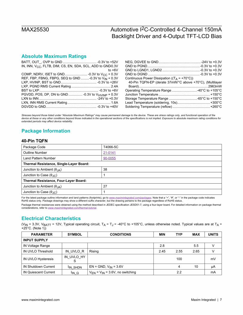
Absolute Maximum RatingsBATT, OUT_, OVP to GND .................................... -0.3V to +52VIN, INN, VCC, FLTB, DIM, CS, EN, SDA, SCL, ADD to GND-0.3V
to +6VCOMP, NDRV, ISET to GND........................ -0.3V to VCC + 0.3VREF, FBP, FBNG, FBPG, SEQ to GND.........-0.3V to VIN + 0.3VLXP, HVINP, BST to GND...................................... -0.3V to +26VLXP, PGND RMS Current Rating .......................................... 2.4ABST to LXP............................................................... -0.3V to +6VPGVDD, POS, DP, DN to GND............... -0.3V to VHVINP + 0.3VLXN to INN ............................................................. -24V to +0.3VLXN, INN RMS Current Rating .............................................. 1.6ADGVDD to GND...................................................... -0.3V to +40V
NEG, DGVEE to GND............................................. -24V to +0.3VGND to PGND........................................................ -0.3V to +0.3VGND to LGND1, LGND2 ........................................ -0.3V to +0.3VGND to DGND ....................................................... -0.3V to +0.3VContinuous Power Dissipation ((TA = +70°C))
40-Pin TQFN-EP (derate 37mW/°C above +70°C), (MultilayerBoard)..........................................................................2963mW
Operating Temperature Range ...........................-40°C to +105°CJunction Temperature .......................................................+150°CStorage Temperature Range ..............................-65°C to +150°CLead Temperature (soldering, 10s)...................................+300°CSoldering Temperature (reflow) ........................................+260°C
Stresses beyond those listed under “Absolute Maximum Ratings” may cause permanent damage to the device. These are stress ratings only, and functional operation of thedevice at these or any other conditions beyond those indicated in the operational sections of the specifications is not implied. Exposure to absolute maximum rating conditions forextended periods may affect device reliability.
Package Information
40-Pin TQFNPackage Code T4066-5COutline Number 21-0141Land Pattern Number 90-0055Thermal Resistance, Single-Layer Board:Junction to Ambient (θJA) 38Junction to Case (θJC) 1Thermal Resistance, Four-Layer Board:Junction to Ambient (θJA) 27Junction to Case (θJC) 1
For the latest package outline information and land patterns (footprints), go to www.maximintegrated.com/packages. Note that a “+”, “#”, or “-” in the package code indicatesRoHS status only. Package drawings may show a different suffix character, but the drawing pertains to the package regardless of RoHS status.Package thermal resistances were obtained using the method described in JEDEC specification JESD51-7, using a four-layer board. For detailed information on package thermalconsiderations, refer to www.maximintegrated.com/thermal-tutorial.
Electrical Characteristics(VIN = 3.3V, VBATT = 12V, Typical operating circuit, TA = TJ = -40°C to +105°C, unless otherwise noted. Typical values are at TA =+25°C. (Note 1))
PARAMETER SYMBOL CONDITIONS MIN TYP MAX UNITSINPUT SUPPLYIN Voltage Range 2.8 5.5 VIN UVLO Threshold IN_UVLO_R Rising 2.45 2.55 2.65 V
IN UVLO Hysteresis IN_UVLO_HYS 100 mV
IN Shutdown Current IIN_SHDN EN = GND, VIN = 3.6V 4 10 µAIN Quiescent Current IIN_Q VEN = VIN = 3.6V, no switching 2.2 mA
MAX25530 Automotive I2C-Controlled 4-Channel 150mABacklight Driver and 4-Output TFT-LCD Bias
www.maximintegrated.com Maxim Integrated | 7
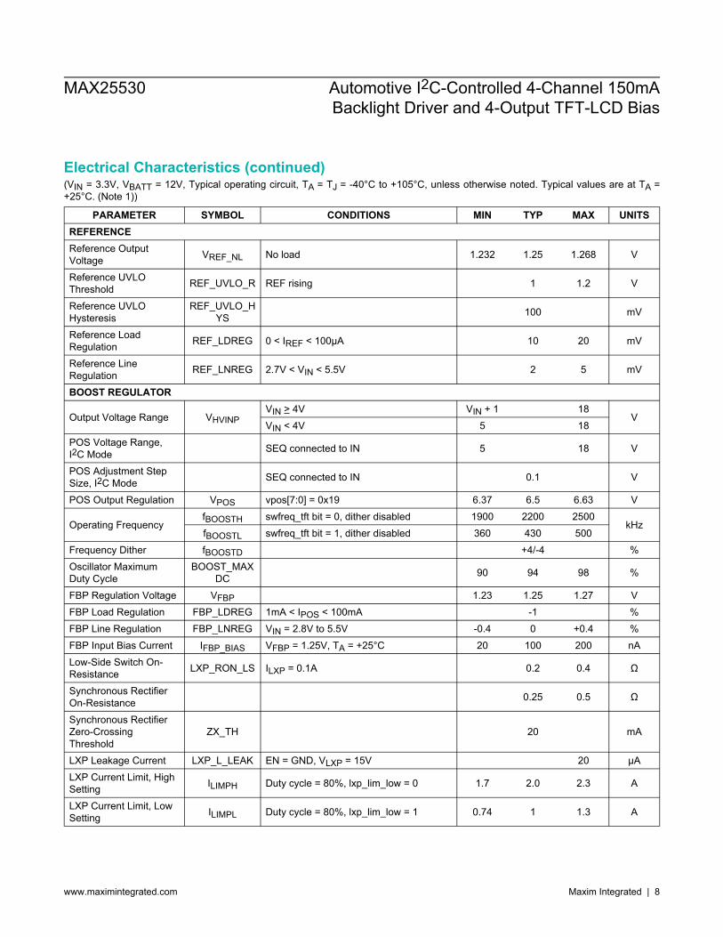
Electrical Characteristics (continued)(VIN = 3.3V, VBATT = 12V, Typical operating circuit, TA = TJ = -40°C to +105°C, unless otherwise noted. Typical values are at TA =+25°C. (Note 1))
PARAMETER SYMBOL CONDITIONS MIN TYP MAX UNITSREFERENCEReference OutputVoltage VREF_NL No load 1.232 1.25 1.268 V
Reference UVLOThreshold REF_UVLO_R REF rising 1 1.2 V
Reference UVLOHysteresis
REF_UVLO_HYS 100 mV
Reference LoadRegulation REF_LDREG 0 < IREF < 100µA 10 20 mV
Reference LineRegulation REF_LNREG 2.7V < VIN < 5.5V 2 5 mV
BOOST REGULATOR
Output Voltage Range VHVINPVIN > 4V VIN + 1 18
VVIN < 4V 5 18
POS Voltage Range,I2C Mode SEQ connected to IN 5 18 V
POS Adjustment StepSize, I2C Mode SEQ connected to IN 0.1 V
POS Output Regulation VPOS vpos[7:0] = 0x19 6.37 6.5 6.63 V
Operating FrequencyfBOOSTH swfreq_tft bit = 0, dither disabled 1900 2200 2500
kHzfBOOSTL swfreq_tft bit = 1, dither disabled 360 430 500
Frequency Dither fBOOSTD +4/-4 %Oscillator MaximumDuty Cycle
BOOST_MAXDC 90 94 98 %
FBP Regulation Voltage VFBP 1.23 1.25 1.27 VFBP Load Regulation FBP_LDREG 1mA < IPOS < 100mA -1 %FBP Line Regulation FBP_LNREG VIN = 2.8V to 5.5V -0.4 0 +0.4 %FBP Input Bias Current IFBP_BIAS VFBP = 1.25V, TA = +25°C 20 100 200 nALow-Side Switch On-Resistance LXP_RON_LS ILXP = 0.1A 0.2 0.4 Ω
Synchronous RectifierOn-Resistance 0.25 0.5 Ω
Synchronous RectifierZero-CrossingThreshold
ZX_TH 20 mA
LXP Leakage Current LXP_L_LEAK EN = GND, VLXP = 15V 20 µALXP Current Limit, HighSetting ILIMPH Duty cycle = 80%, lxp_lim_low = 0 1.7 2.0 2.3 A
LXP Current Limit, LowSetting ILIMPL Duty cycle = 80%, lxp_lim_low = 1 0.74 1 1.3 A
MAX25530 Automotive I2C-Controlled 4-Channel 150mABacklight Driver and 4-Output TFT-LCD Bias
www.maximintegrated.com Maxim Integrated | 8
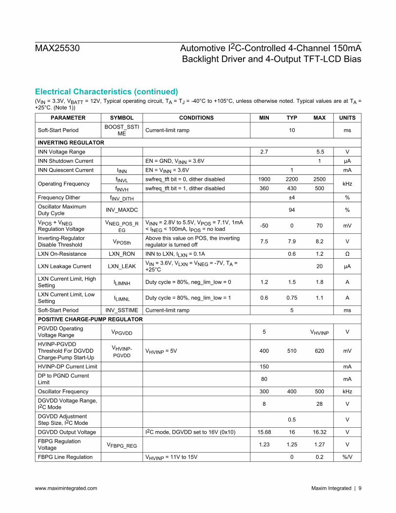
Electrical Characteristics (continued)(VIN = 3.3V, VBATT = 12V, Typical operating circuit, TA = TJ = -40°C to +105°C, unless otherwise noted. Typical values are at TA =+25°C. (Note 1))
PARAMETER SYMBOL CONDITIONS MIN TYP MAX UNITS
Soft-Start Period BOOST_SSTIME Current-limit ramp 10 ms
INVERTING REGULATORINN Voltage Range 2.7 5.5 VINN Shutdown Current EN = GND, VINN = 3.6V 1 µAINN Quiescent Current IINN EN = VINN = 3.6V 1 mA
Operating FrequencyfINVL swfreq_tft bit = 0, dither disabled 1900 2200 2500
kHzfINVH swfreq_tft bit = 1, dither disabled 360 430 500
Frequency Dither fINV_DITH ±4 %Oscillator MaximumDuty Cycle INV_MAXDC 94 %
VPOS + VNEGRegulation Voltage
VNEG_POS_REG
VINN = 2.8V to 5.5V, VPOS = 7.1V, 1mA< INEG < 100mA, IPOS = no load -50 0 70 mV
Inverting-RegulatorDisable Threshold VPOSth
Above this value on POS, the invertingregulator is turned off 7.5 7.9 8.2 V
LXN On-Resistance LXN_RON INN to LXN, ILXN = 0.1A 0.6 1.2 Ω
LXN Leakage Current LXN_LEAK VIN = 3.6V, VLXN = VNEG = -7V, TA =+25°C 20 µA
LXN Current Limit, HighSetting ILIMNH Duty cycle = 80%, neg_lim_low = 0 1.2 1.5 1.8 A
LXN Current Limit, LowSetting ILIMNL Duty cycle = 80%, neg_lim_low = 1 0.6 0.75 1.1 A
Soft-Start Period INV_SSTIME Current-limit ramp 5 msPOSITIVE CHARGE-PUMP REGULATORPGVDD OperatingVoltage Range VPGVDD 5 VHVINP V
HVINP-PGVDDThreshold For DGVDDCharge-Pump Start-Up
VHVINP-PGVDD
VHVINP = 5V 400 510 620 mV
HVINP-DP Current Limit 150 mADP to PGND CurrentLimit 80 mA
Oscillator Frequency 300 400 500 kHzDGVDD Voltage Range,I2C Mode 8 28 V
DGVDD AdjustmentStep Size, I2C Mode 0.5 V
DGVDD Output Voltage I2C mode, DGVDD set to 16V (0x10) 15.68 16 16.32 VFBPG RegulationVoltage VFBPG_REG 1.23 1.25 1.27 V
FBPG Line Regulation VHVINP = 11V to 15V 0 0.2 %/V
MAX25530 Automotive I2C-Controlled 4-Channel 150mABacklight Driver and 4-Output TFT-LCD Bias
www.maximintegrated.com Maxim Integrated | 9
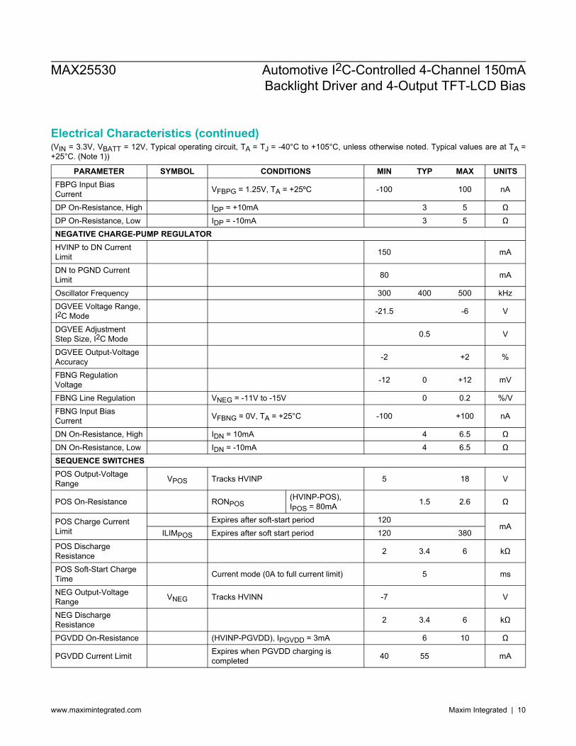
Electrical Characteristics (continued)(VIN = 3.3V, VBATT = 12V, Typical operating circuit, TA = TJ = -40°C to +105°C, unless otherwise noted. Typical values are at TA =+25°C. (Note 1))
PARAMETER SYMBOL CONDITIONS MIN TYP MAX UNITSFBPG Input BiasCurrent VFBPG = 1.25V, TA = +25ºC -100 100 nA
DP On-Resistance, High IDP = +10mA 3 5 ΩDP On-Resistance, Low IDP = -10mA 3 5 ΩNEGATIVE CHARGE-PUMP REGULATORHVINP to DN CurrentLimit 150 mA
DN to PGND CurrentLimit 80 mA
Oscillator Frequency 300 400 500 kHzDGVEE Voltage Range,I2C Mode -21.5 -6 V
DGVEE AdjustmentStep Size, I2C Mode 0.5 V
DGVEE Output-VoltageAccuracy -2 +2 %
FBNG RegulationVoltage -12 0 +12 mV
FBNG Line Regulation VNEG = -11V to -15V 0 0.2 %/VFBNG Input BiasCurrent VFBNG = 0V, TA = +25°C -100 +100 nA
DN On-Resistance, High IDN = 10mA 4 6.5 ΩDN On-Resistance, Low IDN = -10mA 4 6.5 ΩSEQUENCE SWITCHESPOS Output-VoltageRange VPOS Tracks HVINP 5 18 V
POS On-Resistance RONPOS(HVINP-POS),IPOS = 80mA 1.5 2.6 Ω
POS Charge CurrentLimit
Expires after soft-start period 120mA
ILIMPOS Expires after soft start period 120 380POS DischargeResistance 2 3.4 6 kΩ
POS Soft-Start ChargeTime Current mode (0A to full current limit) 5 ms
NEG Output-VoltageRange VNEG Tracks HVINN -7 V
NEG DischargeResistance 2 3.4 6 kΩ
PGVDD On-Resistance (HVINP-PGVDD), IPGVDD = 3mA 6 10 Ω
PGVDD Current Limit Expires when PGVDD charging iscompleted 40 55 mA
MAX25530 Automotive I2C-Controlled 4-Channel 150mABacklight Driver and 4-Output TFT-LCD Bias
www.maximintegrated.com Maxim Integrated | 10
Electrical Characteristics (continued)(VIN = 3.3V, VBATT = 12V, Typical operating circuit, TA = TJ = -40°C to +105°C, unless otherwise noted. Typical values are at TA =+25°C. (Note 1))
PARAMETER SYMBOL CONDITIONS MIN TYP MAX UNITSDGVDD Input VoltageRange 6 22 V
DGVDD DischargeResistance 7 12 17 kΩ
DGVEE Input VoltageRange -22 -6 V
DGVEE DischargeResistance 7 12 17 kΩ
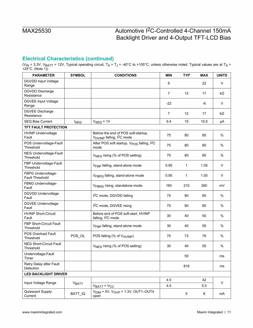
SEQ Bias Current ISEQ VSEQ = 1V 9.4 10 10.5 µATFT FAULT PROTECTIONHVINP UndervoltageFault
Before the end of POS soft-startup,VHVINP falling, I2C mode 75 80 85 %
POS Undervoltage-FaultThreshold
After POS soft startup, VPOS falling, I2Cmode 75 80 85 %
NEG Undervoltage-FaultThreshold VNEG rising (% of POS setting) 75 80 85 %
FBP Undervoltage-FaultThreshold VFBP falling, stand-alone mode 0.95 1 1.05 V
FBPG Undervoltage-Fault Threshold VFBPG falling, stand-alone mode 0.95 1 1.05 V
FBNG Undervoltage-Fault VFBNG rising, standalone mode. 160 210 260 mV
DGVDD UndervoltageFault I2C mode, DGVDD falling 75 80 85 %
DGVEE UndervoltageFault I2C mode, DGVEE rising 75 80 85 %
HVINP Short-CircuitFault
Before end of POS soft-start, HVINPfalling, I2C mode 30 40 50 %
FBP Short-Circuit FaultThreshold VFBP falling, stand-alone mode 30 40 50 %
POS Overload FaultThreshold POS_OL POS falling (% of VHVINP) 70 73 76 %
NEG Short-Circuit FaultThreshold VNEG rising (% of POS setting) 30 40 50 %
Undervoltage-FaultTimer 50 ms
Retry Delay after FaultDetection 818 ms
LED BACKLIGHT DRIVER
Input Voltage Range VBATT4.5 42
VVBATT = VCC 4.5 5.5
Quiescent SupplyCurrent BATT_IQ VDIM = 5V, VOVP = 1.3V, OUT1–OUT4
open 5 8 mA
MAX25530 Automotive I2C-Controlled 4-Channel 150mABacklight Driver and 4-Output TFT-LCD Bias
www.maximintegrated.com Maxim Integrated | 11
Electrical Characteristics (continued)(VIN = 3.3V, VBATT = 12V, Typical operating circuit, TA = TJ = -40°C to +105°C, unless otherwise noted. Typical values are at TA =+25°C. (Note 1))
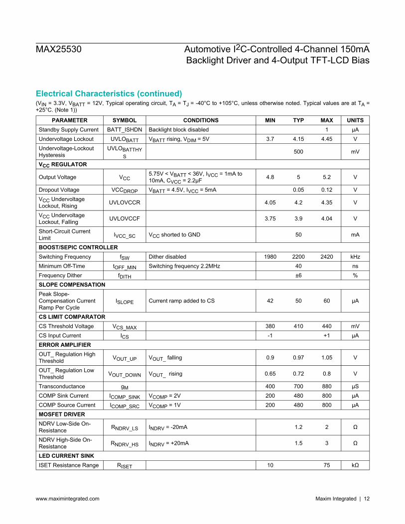
PARAMETER SYMBOL CONDITIONS MIN TYP MAX UNITSStandby Supply Current BATT_ISHDN Backlight block disabled 1 µAUndervoltage Lockout UVLOBATT VBATT rising, VDIM = 5V 3.7 4.15 4.45 VUndervoltage-LockoutHysteresis
UVLOBATTHYS
500 mV
VCC REGULATOR
Output Voltage VCC5.75V < VBATT < 36V, IVCC = 1mA to10mA, CVCC = 2.2μF 4.8 5 5.2 V
Dropout Voltage VCCDROP VBATT = 4.5V, IVCC = 5mA 0.05 0.12 VVCC UndervoltageLockout, Rising UVLOVCCR 4.05 4.2 4.35 V
VCC UndervoltageLockout, Falling UVLOVCCF 3.75 3.9 4.04 V
Short-Circuit CurrentLimit IVCC_SC VCC shorted to GND 50 mA
BOOST/SEPIC CONTROLLERSwitching Frequency fSW Dither disabled 1980 2200 2420 kHzMinimum Off-Time tOFF_MIN Switching frequency 2.2MHz 40 nsFrequency Dither fDITH ±6 %SLOPE COMPENSATIONPeak Slope-Compensation CurrentRamp Per Cycle
ISLOPE Current ramp added to CS 42 50 60 µA
CS LIMIT COMPARATORCS Threshold Voltage VCS_MAX 380 410 440 mVCS Input Current ICS -1 +1 µAERROR AMPLIFIEROUT_ Regulation HighThreshold VOUT_UP VOUT_ falling 0.9 0.97 1.05 V
OUT_ Regulation LowThreshold VOUT_DOWN VOUT_ rising 0.65 0.72 0.8 V
Transconductance gM 400 700 880 µSCOMP Sink Current ICOMP_SINK VCOMP = 2V 200 480 800 µACOMP Source Current ICOMP_SRC VCOMP = 1V 200 480 800 µAMOSFET DRIVERNDRV Low-Side On-Resistance RNDRV_LS INDRV = -20mA 1.2 2 Ω
NDRV High-Side On-Resistance RNDRV_HS INDRV = +20mA 1.5 3 Ω
LED CURRENT SINKISET Resistance Range RISET 10 75 kΩ
MAX25530 Automotive I2C-Controlled 4-Channel 150mABacklight Driver and 4-Output TFT-LCD Bias
www.maximintegrated.com Maxim Integrated | 12
Electrical Characteristics (continued)(VIN = 3.3V, VBATT = 12V, Typical operating circuit, TA = TJ = -40°C to +105°C, unless otherwise noted. Typical values are at TA =+25°C. (Note 1))
PARAMETER SYMBOL CONDITIONS MIN TYP MAX UNITS
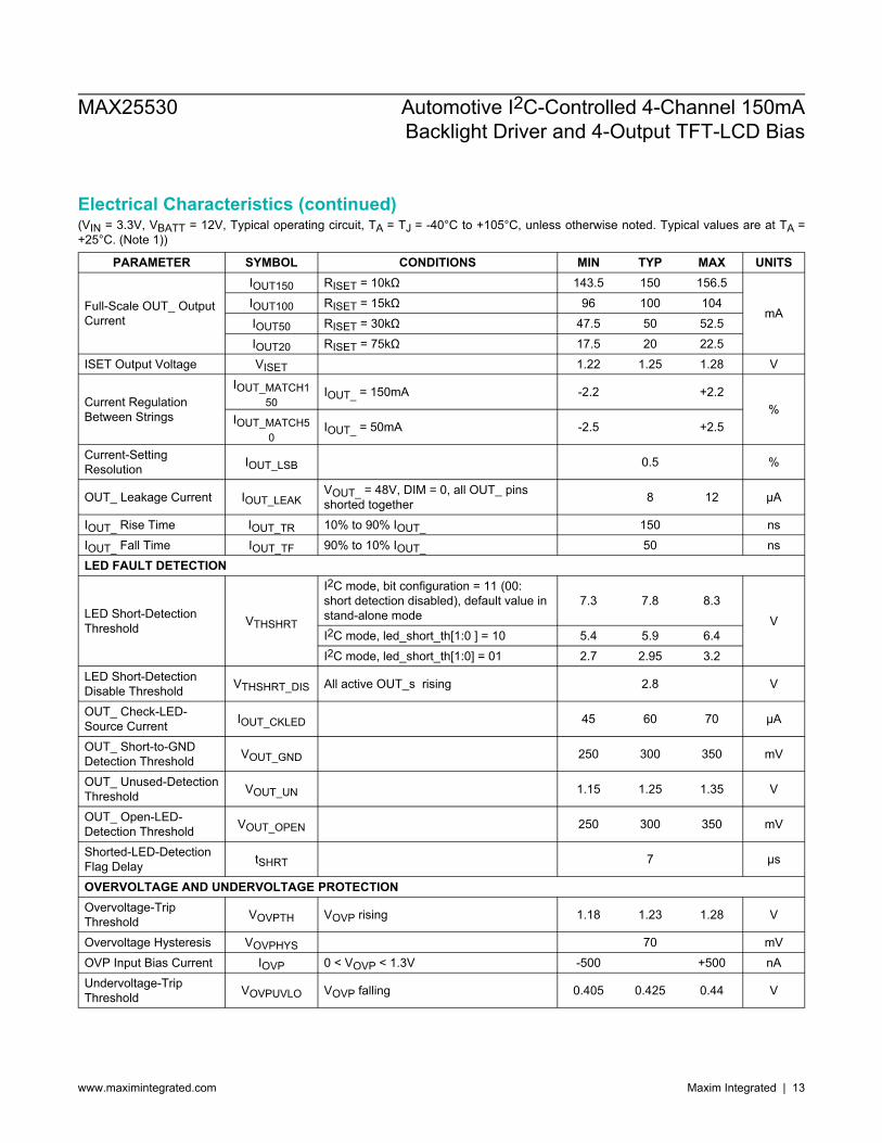
Full-Scale OUT_ OutputCurrent
IOUT150 RISET = 10kΩ 143.5 150 156.5
mAIOUT100 RISET = 15kΩ 96 100 104IOUT50 RISET = 30kΩ 47.5 50 52.5IOUT20 RISET = 75kΩ 17.5 20 22.5
ISET Output Voltage VISET 1.22 1.25 1.28 V
Current RegulationBetween Strings
IOUT_MATCH150
IOUT_ = 150mA -2.2 +2.2%
IOUT_MATCH50
IOUT_ = 50mA -2.5 +2.5
Current-SettingResolution IOUT_LSB 0.5 %
OUT_ Leakage Current IOUT_LEAKVOUT_ = 48V, DIM = 0, all OUT_ pinsshorted together 8 12 µA
IOUT_ Rise Time IOUT_TR 10% to 90% IOUT_ 150 nsIOUT_ Fall Time IOUT_TF 90% to 10% IOUT_ 50 nsLED FAULT DETECTION
LED Short-DetectionThreshold VTHSHRT
I2C mode, bit configuration = 11 (00:short detection disabled), default value instand-alone mode
7.3 7.8 8.3V
I2C mode, led_short_th[1:0 ] = 10 5.4 5.9 6.4I2C mode, led_short_th[1:0] = 01 2.7 2.95 3.2
LED Short-DetectionDisable Threshold VTHSHRT_DIS All active OUT_s rising 2.8 V
OUT_ Check-LED-Source Current IOUT_CKLED 45 60 70 µA
OUT_ Short-to-GNDDetection Threshold VOUT_GND 250 300 350 mV
OUT_ Unused-DetectionThreshold VOUT_UN 1.15 1.25 1.35 V
OUT_ Open-LED-Detection Threshold VOUT_OPEN 250 300 350 mV
Shorted-LED-DetectionFlag Delay tSHRT 7 μs
OVERVOLTAGE AND UNDERVOLTAGE PROTECTIONOvervoltage-TripThreshold VOVPTH VOVP rising 1.18 1.23 1.28 V
Overvoltage Hysteresis VOVPHYS 70 mVOVP Input Bias Current IOVP 0 < VOVP < 1.3V -500 +500 nAUndervoltage-TripThreshold VOVPUVLO VOVP falling 0.405 0.425 0.44 V
MAX25530 Automotive I2C-Controlled 4-Channel 150mABacklight Driver and 4-Output TFT-LCD Bias
www.maximintegrated.com Maxim Integrated | 13
Electrical Characteristics (continued)(VIN = 3.3V, VBATT = 12V, Typical operating circuit, TA = TJ = -40°C to +105°C, unless otherwise noted. Typical values are at TA =+25°C. (Note 1))
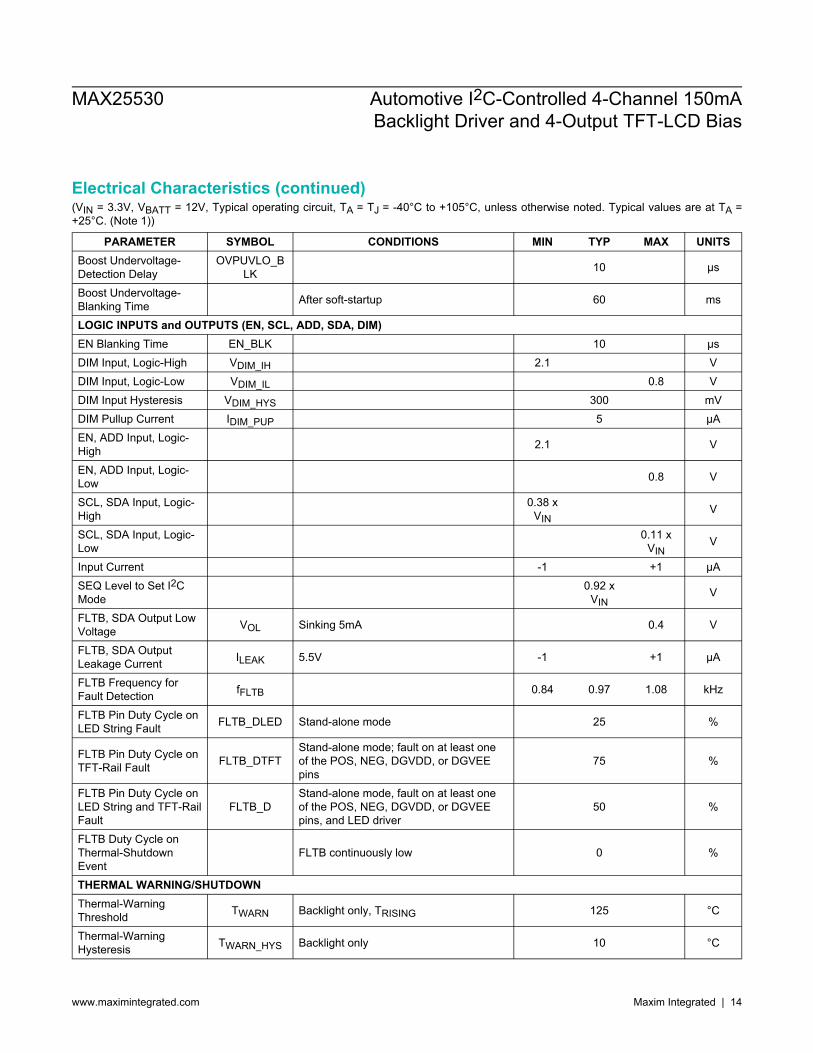
PARAMETER SYMBOL CONDITIONS MIN TYP MAX UNITSBoost Undervoltage-Detection Delay
OVPUVLO_BLK 10 µs
Boost Undervoltage-Blanking Time After soft-startup 60 ms
LOGIC INPUTS and OUTPUTS (EN, SCL, ADD, SDA, DIM)EN Blanking Time EN_BLK 10 µsDIM Input, Logic-High VDIM_IH 2.1 VDIM Input, Logic-Low VDIM_IL 0.8 VDIM Input Hysteresis VDIM_HYS 300 mVDIM Pullup Current IDIM_PUP 5 µAEN, ADD Input, Logic-High 2.1 V
EN, ADD Input, Logic-Low 0.8 V
SCL, SDA Input, Logic-High
0.38 xVIN
V
SCL, SDA Input, Logic-Low
0.11 xVIN
V
Input Current -1 +1 µASEQ Level to Set I2CMode
0.92 xVIN
V
FLTB, SDA Output LowVoltage VOL Sinking 5mA 0.4 V
FLTB, SDA OutputLeakage Current ILEAK 5.5V -1 +1 µA
FLTB Frequency forFault Detection fFLTB 0.84 0.97 1.08 kHz
FLTB Pin Duty Cycle onLED String Fault FLTB_DLED Stand-alone mode 25 %
FLTB Pin Duty Cycle onTFT-Rail Fault FLTB_DTFT
Stand-alone mode; fault on at least oneof the POS, NEG, DGVDD, or DGVEEpins
75 %
FLTB Pin Duty Cycle onLED String and TFT-RailFault
FLTB_DStand-alone mode, fault on at least oneof the POS, NEG, DGVDD, or DGVEEpins, and LED driver
50 %
FLTB Duty Cycle onThermal-ShutdownEvent
FLTB continuously low 0 %
THERMAL WARNING/SHUTDOWNThermal-WarningThreshold TWARN Backlight only, TRISING 125 °C
Thermal-WarningHysteresis TWARN_HYS Backlight only 10 °C
MAX25530 Automotive I2C-Controlled 4-Channel 150mABacklight Driver and 4-Output TFT-LCD Bias
www.maximintegrated.com Maxim Integrated | 14
Electrical Characteristics (continued)(VIN = 3.3V, VBATT = 12V, Typical operating circuit, TA = TJ = -40°C to +105°C, unless otherwise noted. Typical values are at TA =+25°C. (Note 1))
PARAMETER SYMBOL CONDITIONS MIN TYP MAX UNITSThermal-ShutdownThreshold TSHDN TRISING 160 °C
Thermal-ShutdownHysteresis TSHDN_HYS 15 °C
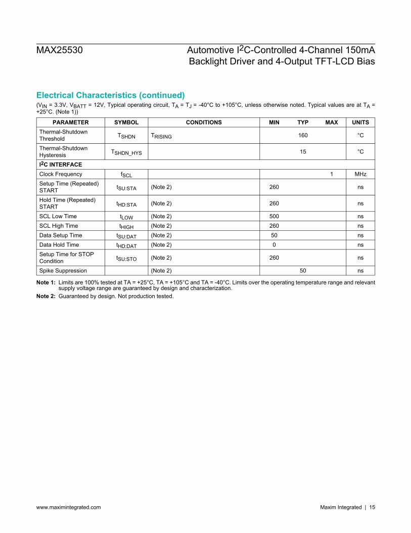
I2C INTERFACEClock Frequency fSCL 1 MHzSetup Time (Repeated)START tSU:STA (Note 2) 260 ns
Hold Time (Repeated)START tHD:STA (Note 2) 260 ns
SCL Low Time tLOW (Note 2) 500 nsSCL High Time tHIGH (Note 2) 260 nsData Setup Time tSU:DAT (Note 2) 50 nsData Hold Time tHD:DAT (Note 2) 0 nsSetup Time for STOPCondition tSU:STO (Note 2) 260 ns
Spike Suppression (Note 2) 50 ns
Note 1: Limits are 100% tested at TA = +25°C, TA = +105°C and TA = -40°C. Limits over the operating temperature range and relevantsupply voltage range are guaranteed by design and characterization.
Note 2: Guaranteed by design. Not production tested.
MAX25530 Automotive I2C-Controlled 4-Channel 150mABacklight Driver and 4-Output TFT-LCD Bias
www.maximintegrated.com Maxim Integrated | 15
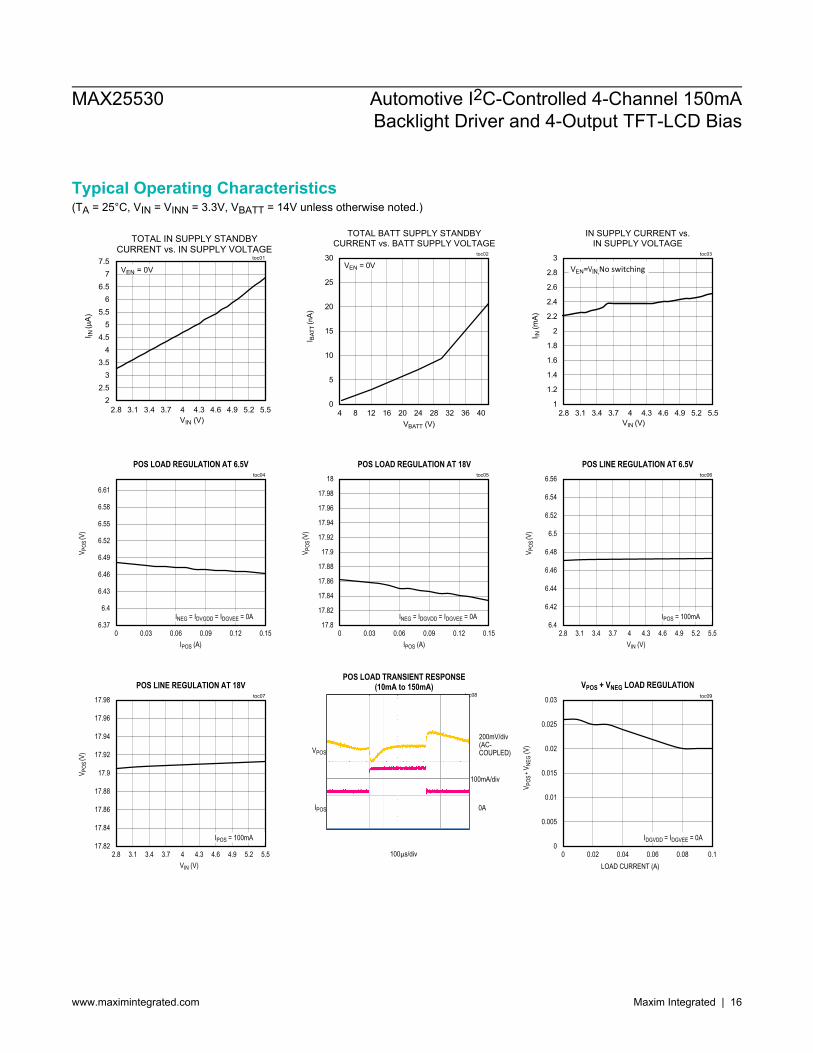
Typical Operating Characteristics(TA = 25°C, VIN = VINN = 3.3V, VBATT = 14V unless otherwise noted.)
MAX25530 Automotive I2C-Controlled 4-Channel 150mABacklight Driver and 4-Output TFT-LCD Bias
www.maximintegrated.com Maxim Integrated | 16
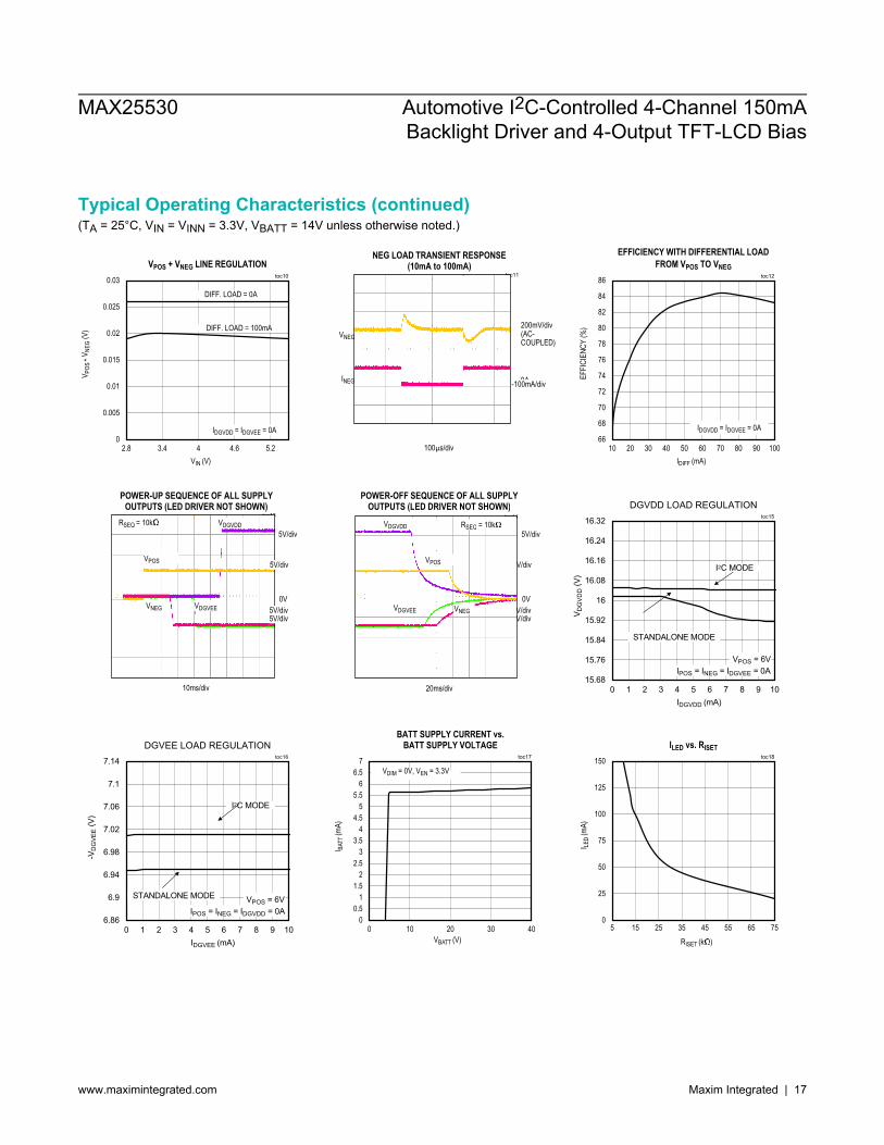
Typical Operating Characteristics (continued)(TA = 25°C, VIN = VINN = 3.3V, VBATT = 14V unless otherwise noted.)
MAX25530 Automotive I2C-Controlled 4-Channel 150mABacklight Driver and 4-Output TFT-LCD Bias
www.maximintegrated.com Maxim Integrated | 17
Typical Operating Characteristics (continued)(TA = 25°C, VIN = VINN = 3.3V, VBATT = 14V unless otherwise noted.)
MAX25530 Automotive I2C-Controlled 4-Channel 150mABacklight Driver and 4-Output TFT-LCD Bias
www.maximintegrated.com Maxim Integrated | 18
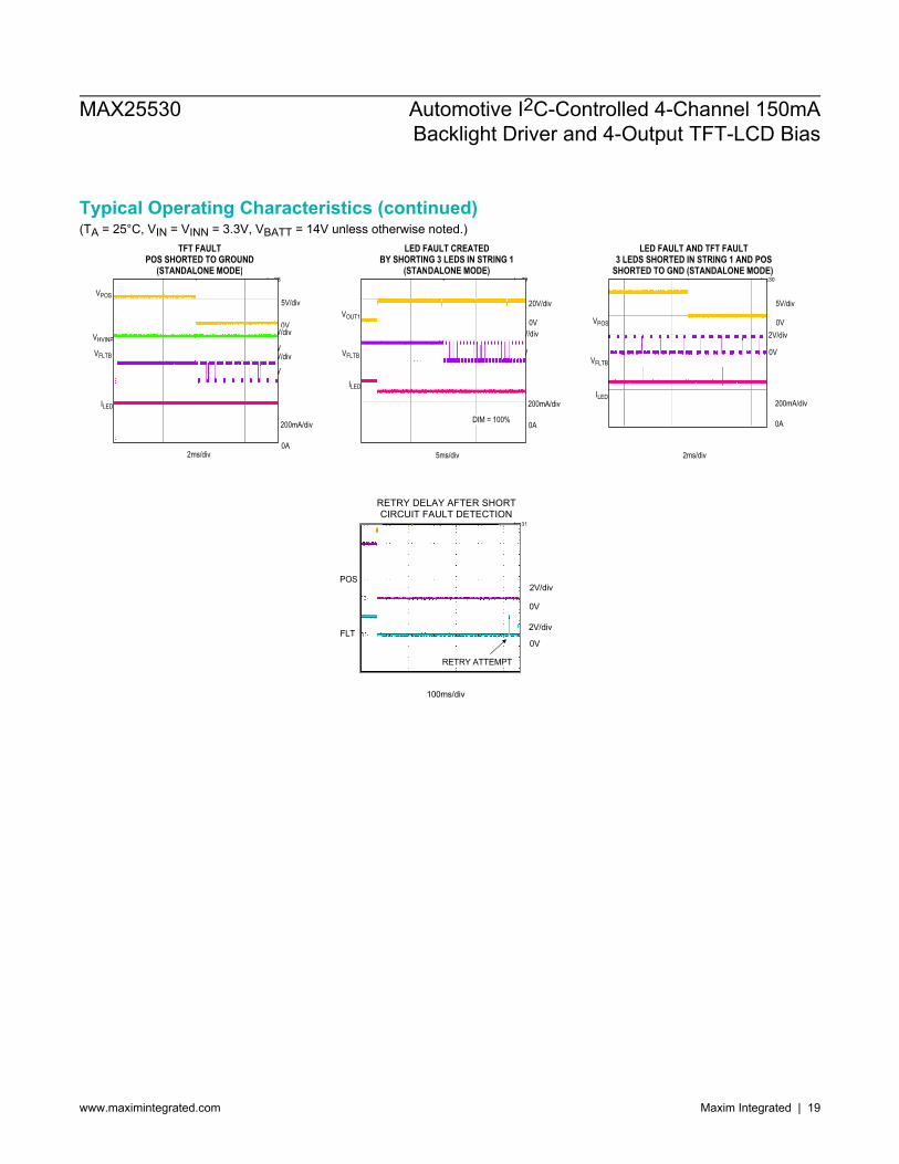
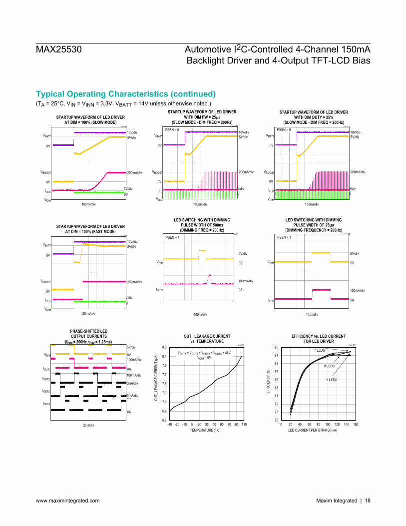
Typical Operating Characteristics (continued)(TA = 25°C, VIN = VINN = 3.3V, VBATT = 14V unless otherwise noted.)
MAX25530 Automotive I2C-Controlled 4-Channel 150mABacklight Driver and 4-Output TFT-LCD Bias
www.maximintegrated.com Maxim Integrated | 19
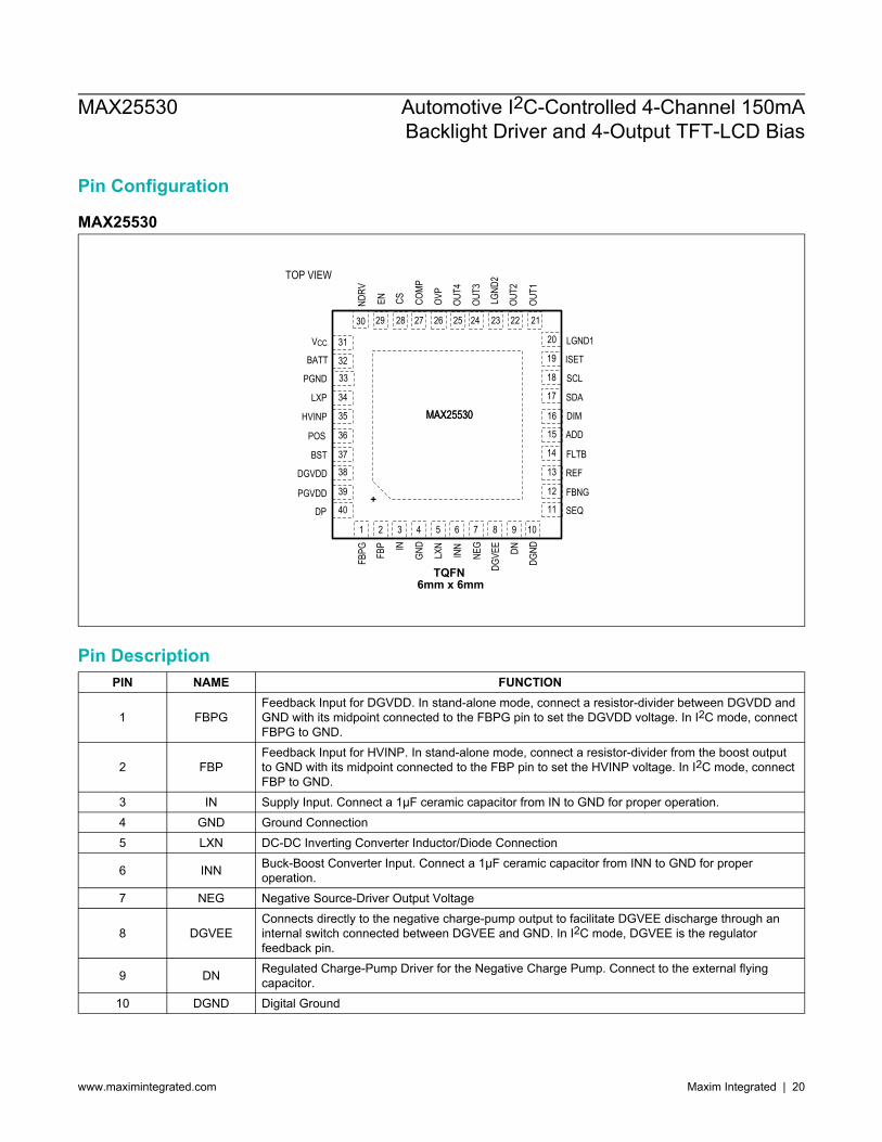
Pin Configuration
MAX25530
TQFN6mm x 6mm
MAXMAX2553025530
TOP VIEW
FBP
GND
LXN
INN
NEG
FBPG
COMP
OUT4
OUT3
CSENNDRV
LGND
2
OUT2
LXP
HVINP
POS
SCL
SDA
DIM
ADD
IN
OVP
BST FLTB
DGVDD
PGVDD
DP
REF
FBNG
SEQ+
PGND
ISETBATT
LGND1
DGVE
E DN
DGND
OUT1
VCC 20
19
18
17
15
14
13
11
31
212223242526272829
10987654321
12
16
3233
34
35
36
3738
39
40
30
Pin DescriptionPIN NAME FUNCTION
1 FBPGFeedback Input for DGVDD. In stand-alone mode, connect a resistor-divider between DGVDD andGND with its midpoint connected to the FBPG pin to set the DGVDD voltage. In I2C mode, connectFBPG to GND.
2 FBPFeedback Input for HVINP. In stand-alone mode, connect a resistor-divider from the boost outputto GND with its midpoint connected to the FBP pin to set the HVINP voltage. In I2C mode, connectFBP to GND.
3 IN Supply Input. Connect a 1μF ceramic capacitor from IN to GND for proper operation.4 GND Ground Connection5 LXN DC-DC Inverting Converter Inductor/Diode Connection
6 INN Buck-Boost Converter Input. Connect a 1μF ceramic capacitor from INN to GND for properoperation.
7 NEG Negative Source-Driver Output Voltage
8 DGVEEConnects directly to the negative charge-pump output to facilitate DGVEE discharge through aninternal switch connected between DGVEE and GND. In I2C mode, DGVEE is the regulatorfeedback pin.
9 DN Regulated Charge-Pump Driver for the Negative Charge Pump. Connect to the external flyingcapacitor.
10 DGND Digital Ground
MAX25530 Automotive I2C-Controlled 4-Channel 150mABacklight Driver and 4-Output TFT-LCD Bias
www.maximintegrated.com Maxim Integrated | 20
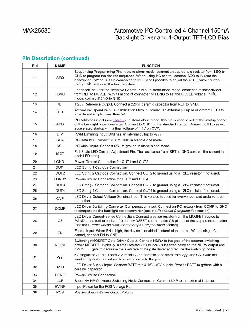
Pin Description (continued)PIN NAME FUNCTION
11 SEQ
Sequencing Programming Pin. In stand-alone mode, connect an appropriate resistor from SEQ toGND to program the desired sequence. When using I2C control, connect SEQ to IN (see thedescription). When SEQ is connected to IN, it is still possible to adjust the OUT_ output currentthrough I2C and read the fault registers.
12 FBNGFeedback Input for the Negative Charge Pump. In stand-alone mode, connect a resistor-dividerfrom REF to DGVEE, with its midpoint connected to FBNG to set the DGVEE voltage. In I2Cmode, connect FBNG to GND.
13 REF 1.25V Reference Output. Connect a 220nF ceramic capacitor from REF to GND.
14 FLTB Active-Low Open-Drain Fault Indication Output. Connect an external pullup resistor from FLTB toan external supply lower than 5V.
15 ADDI2C Address Select (see Table 2). In stand-alone mode, this pin is used to select the startup speedof the backlight boost converter. Connect to GND for the standard startup. Connect to IN to selectaccelerated startup with a final voltage of 1.1V on OVP.
16 DIM PWM Dimming Input. DIM has an internal pullup to VCC.17 SDA I2C Data I/O. Connect SDA to GND in stand-alone mode.18 SCL I2C Clock Input. Connect SCL to ground in stand-alone mode.
19 ISET Full-Scale LED Current-Adjustment Pin. The resistance from ISET to GND controls the current ineach LED string.
20 LGND1 Power-Ground Connection for OUT1 and OUT221 OUT1 LED String 1 Cathode Connection22 OUT2 LED String 2 Cathode Connection. Connect OUT2 to ground using a 12kΩ resistor if not used.23 LGND2 Power-Ground Connection for OUT3 and OUT424 OUT3 LED String 3 Cathode Connection. Connect OUT3 to ground using a 12kΩ resistor if not used.25 OUT4 LED String 4 Cathode Connection. Connect OUT4 to ground using a 12kΩ resistor if not used.
26 OVP LED Driver Output-Voltage-Sensing Input. This voltage is used for overvoltage and undervoltageprotection.
27 COMP LED Driver Switching-Converter Compensation Input. Connect an RC network from COMP to GNDto compensate the backlight boost converter (see the Feedback Compensation section).
28 CSLED Driver Current-Sense Connection. Connect a sense resistor from the MOSFET source toPGND and a further resistor from the MOSFET source to the CS pin to set the slope compensation(see the Current-Sense Resistor and Slope Compensation section).
29 EN Enable Input. When EN is high, the device is enabled in stand-alone mode. When using I2Ccontrol, connect EN to GND.
30 NDRVSwitching nMOSFET Gate-Driver Output. Connect NDRV to the gate of the external switching-power MOSFET. Typically, a small resistor (1Ω to 22Ω) is inserted between the NDRV output andnMOSFET gate to decrease the slew rate of the gate driver and reduce the switching noise.
31 VCC5V Regulator Output. Place 2.2μF and 22nF ceramic capacitors from VCC and GND with thesmaller capacitor placed as close as possible to the pin.
32 BATT LED Driver Supply Input. Connect BATT to a 4.75V–40V supply. Bypass BATT to ground with aceramic capacitor.
33 PGND Power-Ground Connection34 LXP Boost HVINP Converter Switching-Node Connection. Connect LXP to the external inductor.35 HVINP Input Power for the POS Voltage Rail36 POS Positive Source-Driver Output Voltage
MAX25530 Automotive I2C-Controlled 4-Channel 150mABacklight Driver and 4-Output TFT-LCD Bias
www.maximintegrated.com Maxim Integrated | 21
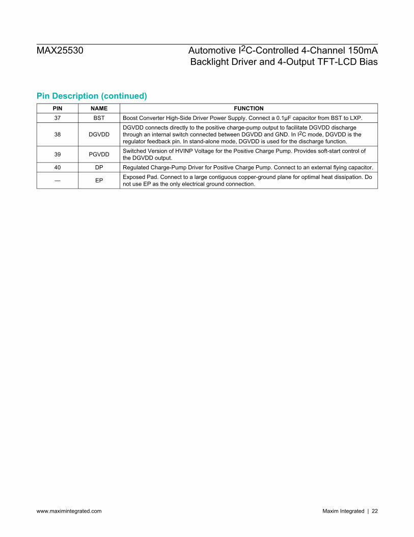
Pin Description (continued)PIN NAME FUNCTION37 BST Boost Converter High-Side Driver Power Supply. Connect a 0.1μF capacitor from BST to LXP.
38 DGVDDDGVDD connects directly to the positive charge-pump output to facilitate DGVDD dischargethrough an internal switch connected between DGVDD and GND. In I2C mode, DGVDD is theregulator feedback pin. In stand-alone mode, DGVDD is used for the discharge function.
39 PGVDD Switched Version of HVINP Voltage for the Positive Charge Pump. Provides soft-start control ofthe DGVDD output.
40 DP Regulated Charge-Pump Driver for Positive Charge Pump. Connect to an external flying capacitor.
— EP Exposed Pad. Connect to a large contiguous copper-ground plane for optimal heat dissipation. Donot use EP as the only electrical ground connection.
MAX25530 Automotive I2C-Controlled 4-Channel 150mABacklight Driver and 4-Output TFT-LCD Bias
www.maximintegrated.com Maxim Integrated | 22
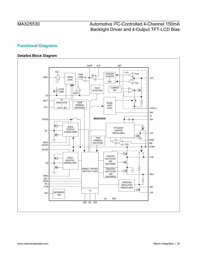
Functional Diagrams
Detailed Block Diagram
MAX25530
BATT
VCC
NDRV
COMP
CS
OVP ISET
DIM
OUT_
LXP
POSITIVE SOFT-START
AND DISCHARGE
HVINP
POS
NEG
INVERTINGREGULATOR
430kHz/2.2MHz
LXN
INN
ENABLE, CONTROL AND FAULT LOGIC
EP
ENDGNDSEQ
400kHz POSITIVE
CHARGE PUMP
400kHz NEGATIVE
CHARGE PUMP DN
DP
PGVDDIN
DGVEE
DGVDDFBPG
FBNG
REF REFERENCE1.25V
LGND1,2
SCL SDA
TFT BOOST CONTROL
430kHz/2.2MHz
I2C
FLTB
GND
NEGATIVE SOFT-START
AND DISCHARGE
ADD
BST
1 of 4 VTHH
VTHL
UP/DOWN COUNTER
+ DAC
gM
CURRENTREF.
DRIVELOGIC
PWMCOMP
5V REGULATOR
+UVLO + BG
VCC
SLOPECOMP 420mV
PHASE-SHIFTLOGIC
TEMP WARNING,
SHUTDOWN
FAULTDETECTION
FBPPGND
1.25V
TEMP WARNING,
SHUTDOWN
MAX25530 Automotive I2C-Controlled 4-Channel 150mABacklight Driver and 4-Output TFT-LCD Bias
www.maximintegrated.com Maxim Integrated | 23
Detailed DescriptionThe MAX25530 is a highly integrated TFT power supply and LED backlight driver IC for automotive TFT-LCDapplications. The IC integrates one buck-boost converter, one boost converter, two gate-driver supplies, and a boost/SEPIC converter that can power one to four strings of LEDs in the display backlight.The source-driver power supplies consist of a synchronous boost converter and an inverting buck-boost converterthat can generate voltages up to +18V and down to -7V. The positive source-driver can deliver up to 120mA, whilethe negative source driver is capable of 100mA. The positive source-driver-supply regulation voltage (VPOS) is set byconnecting an external resistor-divider on FBP or through I2C. The negative source-driver-supply voltage (VNEG) isalways tightly regulated to -VPOS (down to a minimum of -7V). The source-driver supplies operate from an input voltagebetween 2.8V and 5.5V.The gate-driver-power supplies consist of regulated charge pumps that generate between +28V and -21.5V and can eachdeliver 10mA or more each, depending on the exact configuration.The IC features a quad-string LED driver that operates from a separate input voltage (BATT) and can power up to fourstrings of LEDs with 150mA (max) of current per string. The IC features logic-controlled pulse-width modulation (PWM)dimming, with minimum pulse widths as low as 500ns and the option of phase shifting the LED strings with respect toone another. When phase shifting is enabled, each string is turned on at a different time, reducing the input and outputripple, as well as audible noise. With phase shifting disabled, each current sink turns on at the same time and allowsparallel connection of current sinks.The startup and shutdown sequences for all power domains are controlled using one of the seven preset modes thatare selectable through a resistor on SEQ. If the SEQ pin is connected to IN (I2C control), any sequence can becontrolled using the individual regulator-enable bits. When a regulator other than HVINP is enabled, the HVINP boost isautomatically enabled (if not previously active). In this case, the second regulator is enabled when the soft-start of HVINPhas completed.
TFT Power Section
Source-Driver Power SuppliesThe source-driver power supplies consist of a boost converter with output switch and an inverting buck-boost converterthat generates up to +18V (max) and down to -7V (min), respectively, and can deliver up to 120mA on the positiveregulator and -100mA on the negative regulator. The positive source-driver power supply’s regulation voltage (VPOS) canbe set by the resistor-divider on FBP or through the I2C interface.The negative source-driver supply voltage (VNEG) is automatically tightly regulated to -VPOS. VNEG cannot be adjustedindependently of VPOS. In I2C mode, VPOS (and VNEG) is set by writing to the appropriate register. When HVINP is setto a voltage greater than 7V in I2C mode, the NEG converter should be disabled to avoid damage to the device. If theNEG output is not needed, the external components can be omitted and INN should be connected to IN; LXN should beleft open and NEG should be connected to GND.
Gate-Driver Power SuppliesThe positive gate-driver power supply (DGVDD) generates +28V (max) and the negative gate-driver power supply(DGVEE) generates -21.5V (min). The maximum output currents depend on the number of charge-pump stages andthe POS setting. The DGVDD and DGVEE regulation voltages are set independently using external resistor networks orthrough the I2C interface.
Fault ProtectionThe IC has robust fault and overload protection. In stand-alone mode, if any of the DGVEE, NEG, POS, or DGVDDoutputs fall to less than 80% (typ) of their intended regulation voltage for more than 50ms (typ), or if a short-circuitcondition occurs on any output for any duration, then the faulted rail latches off, the other outputs follow the turn-offsequence and a fault condition is set. In I2C mode, only the output at fault is automatically disabled.
MAX25530 Automotive I2C-Controlled 4-Channel 150mABacklight Driver and 4-Output TFT-LCD Bias
www.maximintegrated.com Maxim Integrated | 24
In stand-alone mode, the fault condition is cleared when the EN pin or IN supply are cycled. In I2C mode, the faultcondition is cleared when the EN bit of the affected rail is set to 0 or the IN supply is cycled.Both sections (TFT and WLED) have thermal-fault detection; only the section causing the thermal overload is turned off.Thermal faults are cleared when the die temperature drops by 15°C.When a fault is detected, FLTB goes low in I2C mode, while in stand-alone mode the FLTB output pulses at a duty cyclethat indicates the source of the fault.After fault detection, a retry timer is started and after 818ms the device attempts to re-start with the programmedsequence or that set by the SEQ pin. If the fault persists the device will again shut down and re-start the retry time unlessthe EN pin is taken low.
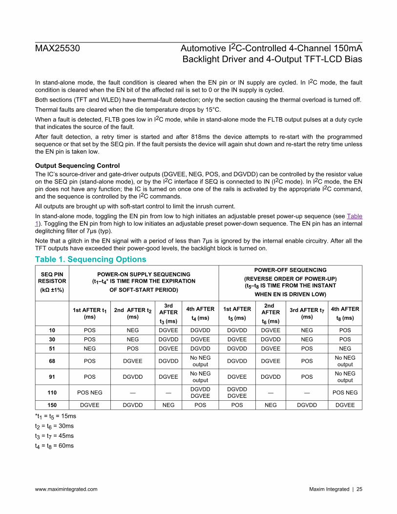
Output Sequencing ControlThe IC’s source-driver and gate-driver outputs (DGVEE, NEG, POS, and DGVDD) can be controlled by the resistor valueon the SEQ pin (stand-alone mode), or by the I2C interface if SEQ is connected to IN (I2C mode). In I2C mode, the ENpin does not have any function; the IC is turned on once one of the rails is activated by the appropriate I2C command,and the sequence is controlled by the I2C commands.All outputs are brought up with soft-start control to limit the inrush current.In stand-alone mode, toggling the EN pin from low to high initiates an adjustable preset power-up sequence (see Table1). Toggling the EN pin from high to low initiates an adjustable preset power-down sequence. The EN pin has an internaldeglitching filter of 7μs (typ).Note that a glitch in the EN signal with a period of less than 7μs is ignored by the internal enable circuitry. After all theTFT outputs have exceeded their power-good levels, the backlight block is turned on.
Table 1. Sequencing OptionsSEQ PIN
RESISTOR(kΩ ±1%)
POWER-ON SUPPLY SEQUENCING(t1–t4* IS TIME FROM THE EXPIRATION
OF SOFT-START PERIOD)
POWER-OFF SEQUENCING(REVERSE ORDER OF POWER-UP)(t5–t8 IS TIME FROM THE INSTANT
WHEN EN IS DRIVEN LOW)
1st AFTER t1(ms)
2nd AFTER t2(ms)
3rdAFTERt3 (ms)
4th AFTERt4 (ms)
1st AFTERt5 (ms)
2ndAFTERt6 (ms)
3rd AFTER t7(ms)
4th AFTERt8 (ms)
10 POS NEG DGVEE DGVDD DGVDD DGVEE NEG POS30 POS NEG DGVDD DGVEE DGVEE DGVDD NEG POS51 NEG POS DGVEE DGVDD DGVDD DGVEE POS NEG
68 POS DGVEE DGVDD No NEGoutput DGVDD DGVEE POS No NEG
output
91 POS DGVDD DGVEE No NEGoutput DGVEE DGVDD POS No NEG
output
110 POS NEG — — DGVDDDGVEE
DGVDDDGVEE — — POS NEG
150 DGVEE DGVDD NEG POS POS NEG DGVDD DGVEE
*t1 = t5 = 15mst2 = t6 = 30mst3 = t7 = 45mst4 = t8 = 60ms
MAX25530 Automotive I2C-Controlled 4-Channel 150mABacklight Driver and 4-Output TFT-LCD Bias
www.maximintegrated.com Maxim Integrated | 25
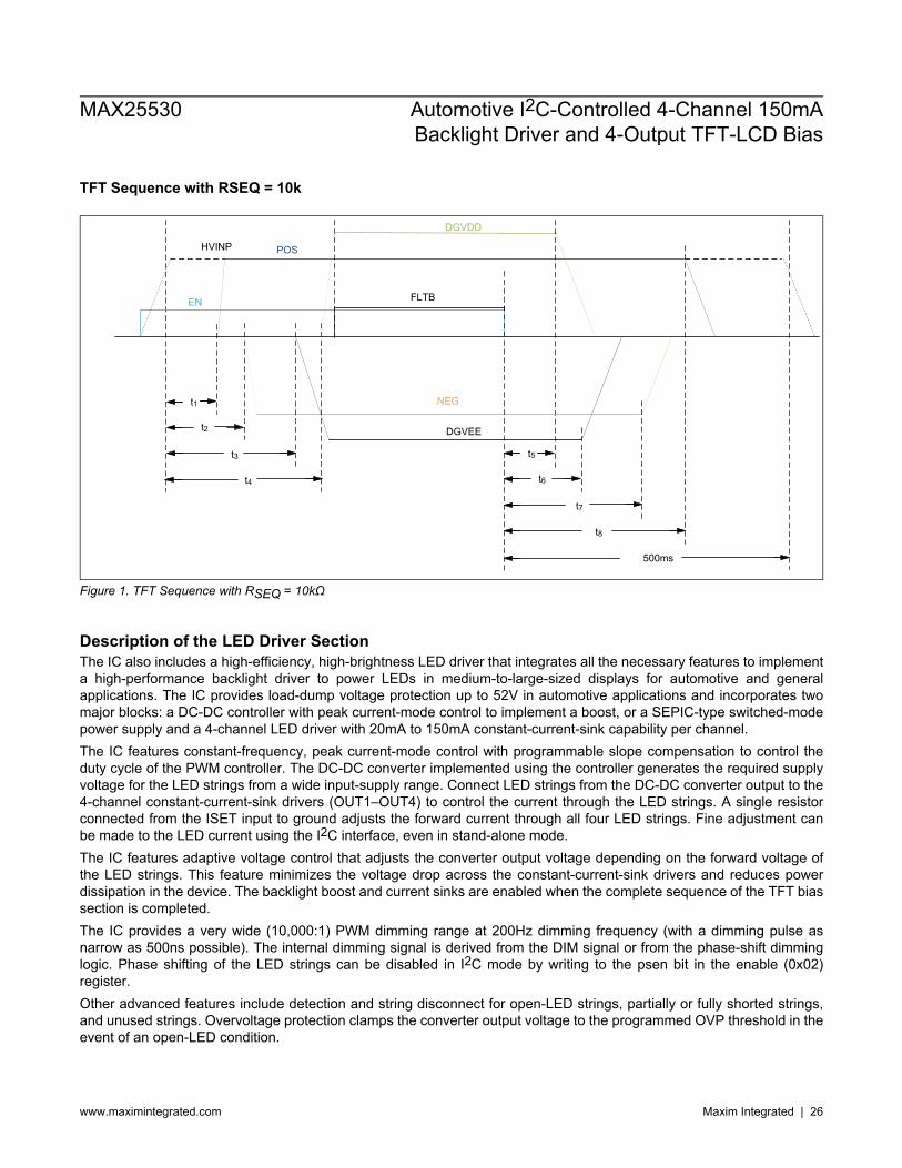
TFT Sequence with RSEQ = 10k
FLTB
HVINP
EN
NEG
DGVEE
POS
DGVDD
t1
t2
t3
t4
t5
t6
t7
t8
500ms
Figure 1. TFT Sequence with RSEQ = 10kΩ
Description of the LED Driver SectionThe IC also includes a high-efficiency, high-brightness LED driver that integrates all the necessary features to implementa high-performance backlight driver to power LEDs in medium-to-large-sized displays for automotive and generalapplications. The IC provides load-dump voltage protection up to 52V in automotive applications and incorporates twomajor blocks: a DC-DC controller with peak current-mode control to implement a boost, or a SEPIC-type switched-modepower supply and a 4-channel LED driver with 20mA to 150mA constant-current-sink capability per channel.The IC features constant-frequency, peak current-mode control with programmable slope compensation to control theduty cycle of the PWM controller. The DC-DC converter implemented using the controller generates the required supplyvoltage for the LED strings from a wide input-supply range. Connect LED strings from the DC-DC converter output to the4-channel constant-current-sink drivers (OUT1–OUT4) to control the current through the LED strings. A single resistorconnected from the ISET input to ground adjusts the forward current through all four LED strings. Fine adjustment canbe made to the LED current using the I2C interface, even in stand-alone mode.The IC features adaptive voltage control that adjusts the converter output voltage depending on the forward voltage ofthe LED strings. This feature minimizes the voltage drop across the constant-current-sink drivers and reduces powerdissipation in the device. The backlight boost and current sinks are enabled when the complete sequence of the TFT biassection is completed.The IC provides a very wide (10,000:1) PWM dimming range at 200Hz dimming frequency (with a dimming pulse asnarrow as 500ns possible). The internal dimming signal is derived from the DIM signal or from the phase-shift dimminglogic. Phase shifting of the LED strings can be disabled in I2C mode by writing to the psen bit in the enable (0x02)register.Other advanced features include detection and string disconnect for open-LED strings, partially or fully shorted strings,and unused strings. Overvoltage protection clamps the converter output voltage to the programmed OVP threshold in theevent of an open-LED condition.
MAX25530 Automotive I2C-Controlled 4-Channel 150mABacklight Driver and 4-Output TFT-LCD Bias
www.maximintegrated.com Maxim Integrated | 26
The shorted-LED string threshold is programmable using the led_short_th[1:0] bits in the cnfg_gen (0x01 register (instand-alone mode, the threshold is fixed at 7.8V).In I2C mode, the FLTB signal asserts low to indicate open-LED, shorted-LED, and overtemperature conditions if theyare not masked. In stand-alone mode, a fault in the backlight section causes FLTB to pulse at 25% duty cycle. Disableindividual current-sink channels by connecting the corresponding OUT_ to LGND_ through a 12kΩ resistor (startingwith OUT4). In this case, FLTB will not indicate an open-LED condition for the disabled channel. The IC also featuresovertemperature warning and protection that shuts down the controller if the die temperature exceeds +160°C.
Current-Mode DC-DC ControllerThe IC backlight boost is a constant-frequency, current-mode controller designed to drive the LEDs in a boost or SEPICconfiguration. The IC features multiloop control to regulate the peak current in the inductor, as well as the voltage acrossthe LED current sinks to minimize power dissipation.The default switching frequency is 2.2MHz but this can be reduced to 440kHz by setting the bl_swfreq bit in the cnfg_gen(0x01) register. Programmable slope compensation is used to avoid subharmonic oscillation that can occur at > 50% dutycycles in continuous-conduction mode.The external nMOSFET is turned on at the beginning of every switching cycle. The inductor current ramps up linearlyuntil turned off at the peak current level set by the feedback loop. The peak inductor current is sensed from the voltageacross the current-sense resistor (RCS) connected from the source of the external nMOSFET to PGND.The IC features leading-edge blanking to suppress the external nMOSFET switching noise. A PWM comparatorcompares the current-sense voltage plus the slope-compensation signal with the output of the transconductance erroramplifier. The controller turns off the external nMOSFET when the voltage at CS exceeds the error amplifier’s outputvoltage (at the COMP pin). This process repeats every switching cycle to achieve peak current-mode control.In addition to the peak current-mode-control loop, the IC has two other feedback loops for control. The converter outputvoltage is sensed through the OVP input, which goes to the inverting input of the error amplifier.The OVP gain (AOVP) is defined as VOUT/VOVP, or (R17 + R16)/R16. The other feedback comes from the OUT_current sinks. This loop controls the headroom of the current sinks to minimize total power dissipation, while still ensuringaccurate LED current matching. Each current sink has a window comparator with a low threshold of 0.68V and a highthreshold of 0.93V. These comparators drive logic that controls an up/down counter. The up/down counter is updated onevery falling edge of the DIM input and drives an 8-bit digital-to-analog converter (DAC), which sets the reference to theerror amplifier.
8-Bit DACThe error amplifier’s reference input is controlled with an 8-bit DAC. The DAC output is ramped up during startup toimplement a soft-start function (see the Startup Sequence section). During normal operation, the DAC output range islimited to between 0.6V and 1.25V. The DAC LSB determines the minimum output-voltage step according to the followingequation.Equation 1:VSTEP_MIN = VDAC_LSB × AOVP
where VSTEP_MIN is the minimum output-voltage step, VDAC_LSB is 2.5mV (typ), and AOVP is the OVP resistor-dividergain.
PWM DimmingThe DIM input accepts a pulse-width modulation (PWM) signal to control the luminous intensity of the LEDs and modulatethe pulse width of the LED current. This allows for changing the brightness of the LEDs without the color temperatureshift that sometimes occurs with analog dimming. The DIM input detects the dimming frequency based on the first twopulses applied to the DIM input after EN goes high. The dimming frequency cannot be changed during normal operation.If a change of dimming frequency is desired, disable the backlight block, change the DIM frequency, and then re-enablethe backlight block. The DIM signal can be applied before or after the device is enabled, but must power on smoothly(no high-frequency pulses). If the DIM signal turn-on is inconsistent, the DIM signal should be applied first; once the DIM
MAX25530 Automotive I2C-Controlled 4-Channel 150mABacklight Driver and 4-Output TFT-LCD Bias
www.maximintegrated.com Maxim Integrated | 27

signal is stable, the backlight block can be enabled. In normal dimming mode, if at least one of the LED current sinksis turned on, the boost converter switches. If none of the current sinks are on (each current-sink DIM signal is low), theboost converter stops switching, and the COMP node is disconnected from the error amplifier until one of the LED currentsinks is turned on again.
Low-Dim ModeThe IC's operation mode changes at very narrow dimming pulses to ensure a consistent dimming response of the LEDs.The IC checks the pulse width of the signal being applied to the DIM input, and if the dimming on-time is lower than25μs (typ) for the 2.2MHz switching frequency (fSW), the IC enters low-dim mode. In this state, the converter switchescontinuously and the LED short detection is disabled. When the DIM input is greater than 26μs (typ) for 2.2MHz, the ICgoes back into normal dim mode, enabling the short-LED detection and switching the power FET only when the DIMsignal is high. When the switching frequency is set to 440kHz the low-dim thresholds become 50μs and 51μs.
Phase ShiftingThe IC offers phase shifting of the LED strings. To achieve this, the DIM signal is sampled internally by a 10MHz clock.When phase shifting is enabled, the sampled DIM input is used to generate separate dimming signals for each LED stringthat is shifted in phase. The resolution with which the DIM signal is captured degrades at higher DIM input frequencies;therefore, dimming frequencies between 100Hz and 3kHz are recommended, although higher dimming frequencies aretechnically possible. The phase shift between strings is determined by the following equation.Equation 2:
Θ = 360n
where n is the total number of strings being used and θ is the phase shift in degrees. The order of the sequence is fixed,with OUT1 as the first in the sequence and OUT4 as the last. See Figure 2 for a timing diagram example with phaseshifting enabled.The phase-shifting feature is enabled or disabled with the psen bit. In stand-alone mode (no I2C), the psen bit in register0x02 is set high by default (phase shifting enabled). When phase shifting is disabled, all strings turn on/off at the sametime. If multiple current sinks are being connected in parallel to achieve greater than 150mA per string, phase shiftingshould be disabled.If a fault is detected, resulting in a string being disabled during normal operation, the phase shifting does not adjust. Forexample, if all four strings are used, each string is 90 degrees out-of-phase. If the fourth string is disabled due to a fault,there will still be 90 degrees phase difference between each string.When disabling unused strings, disable the higher-numbered OUT_ current sinks first.
MAX25530 Automotive I2C-Controlled 4-Channel 150mABacklight Driver and 4-Output TFT-LCD Bias
www.maximintegrated.com Maxim Integrated | 28
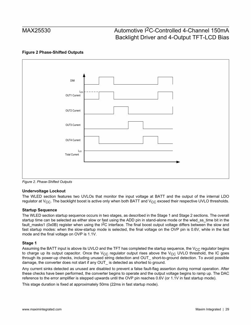
Figure 2 Phase-Shifted Outputs
OUT1 Current
OUT2 Current
OUT3 Current
OUT4 Current
Total Current
DIM
ILED
ILED
Figure 2. Phase-Shifted Outputs
Undervoltage LockoutThe WLED section features two UVLOs that monitor the input voltage at BATT and the output of the internal LDOregulator at VCC. The backlight boost is active only when both BATT and VCC exceed their respective UVLO thresholds.
Startup SequenceThe WLED section startup sequence occurs in two stages, as described in the Stage 1 and Stage 2 sections. The overallstartup time can be selected as either slow or fast using the ADD pin in stand-alone mode or the wled_ss_time bit in thefault_masks1 (0x0B) register when using the I2C interface. The final boost output voltage differs between the slow andfast startup modes: when the slow-startup mode is selected, the final voltage on the OVP pin is 0.6V, while in the fastmode and the final voltage on OVP is 1.1V.
Stage 1Assuming the BATT input is above its UVLO and the TFT has completed the startup sequence, the VCC regulator beginsto charge up its output capacitor. Once the VCC regulator output rises above the VCC UVLO threshold, the IC goesthrough its power-up checks, including unused string detection and OUT_ short-to-ground detection. To avoid possibledamage, the converter does not start if any OUT_ is detected as shorted to ground.Any current sinks detected as unused are disabled to prevent a false fault-flag assertion during normal operation. Afterthese checks have been performed, the converter begins to operate and the output voltage begins to ramp up. The DACreference to the error amplifier is stepped upwards until the OVP pin reaches 0.6V (or 1.1V in fast startup mode).This stage duration is fixed at approximately 50ms (22ms in fast startup mode).
MAX25530 Automotive I2C-Controlled 4-Channel 150mABacklight Driver and 4-Output TFT-LCD Bias
www.maximintegrated.com Maxim Integrated | 29

Stage 2The second stage begins once the first stage is complete and the DIM input goes high. During Stage 2, the output ofthe converter is adjusted until the minimum OUT_ voltage falls within the window comparator limits of 0.68V (typ) and0.93V (typ). The output ramp is again controlled by the DAC, which provides the reference for the error amplifier. TheDAC output is updated on each rising edge of the DIM input. If the DIM input is a 100% duty cycle (DIM = high), then theDAC output is updated once every 10ms.The total soft-start time can be calculated using the following equation in slow-startup mode.Equation 3:
tSS = 50ms +VLED + 0.81 − (0.6 × AOVP)
fDIM × 0.01 × AOVP
where tSS is the total soft-start time, 50ms is the fixed Stage 1 duration, VLED is the total forward voltage of the LEDstrings, 0.81V is midpoint of the window comparator, AOVP is the gain of the OVP resistor-divider, fDIM is the dimmingfrequency (use 100Hz if the DIM input duty cycle is 100%), and 0.01V is the maximum voltage step per clock cycle of theDAC.In fast-startup mode (with ADD connected to IN or the wled_ss_time bit in the fault_masks1 (0x0B) register set to 1), thefollowing equation should be used.Equation 4:
tSS = 22ms +1.1 × AOVP − (VLED + 0.81)
fDIM × 0.01 × AOVP
Open-LED Management and Overvoltage Protection (OVP)On power-up, the IC detects and disconnects any unused current-sink channels before entering the DC-DC convertersoft-start. Disable the unused current-sink channels by connecting the corresponding OUT_ to LGND_ through a 12kΩresistor. This avoids asserting the FLTB output for the unused channels. After soft-start, the IC detects open strings anddisconnects them from the internal minimum OUT_ voltage detector. This keeps the DC-DC converter output voltagewithin safe limits and maintains high efficiency.If any LED string is open, the voltage at the open OUT_ goes to GND. The DC-DC converter output voltage thenincreases to the overvoltage-protection threshold set by the voltage-divider network connected between the converteroutput, OVP input, and GND (the threshold at which the PWM controller is switched off, holding NDRV low). At that point,any current-sink output with VOUT_ < 300mV (typ) is disconnected from the minimum-voltage detector. Select VOUT_OVP(which will be the maximum voltage that the boost converter can produce) according to the following equation.Equation 5:VOUT_OVP > 1.1 × (VLED_MAX + 1)
where VLED_MAX is the maximum expected LED string voltage. VOUT_OVP should also be chosen such that the voltageat the OUT_ pins does not exceed the absolute maximum rating.The upper resistor in the OVP resistor-divider (R17) can be selected using the following formula.Equation 6:
R17 = R16 × (VOUT_OVP
1.23 − 1)
where 1.23V is the typical OVP threshold. Ensure that the minimum voltage on the OVP pin is always greater than 0.6Vto avoid the boost converter latching off due to undervoltage by checking the following.Equation 7:
(VLED_MIN + 0.6) × R16R16 + R17 > 0.6V
where VLED_MIN is the worst-case minimum LED string voltage.
MAX25530 Automotive I2C-Controlled 4-Channel 150mABacklight Driver and 4-Output TFT-LCD Bias
www.maximintegrated.com Maxim Integrated | 30
When an open-LED condition occurs, FLTB is asserted low in I2C mode or switches at 25% in stand-alone mode.For boost-circuit applications, the OVP resistor-divider always dissipates power from the battery, through the inductorand switching diode. If ultra-low shutdown current is needed in stand-alone mode, a general-purpose MOSFET can beadded between the bottom OVP resistor and ground, with the EN of the device controlling the gate of the MOSFET. Thisadditional MOSFET disconnects the OVP resistor-divider path when the device is disabled.
Short-LED DetectionThe IC checks for shorted LEDs at each rising edge of DIM. An LED short is detected at OUT_ if the OUT_ voltage isgreater than the value programmed using the led_short_th bits in register 0x01 (or 7.8V in stand-alone mode). Once ashort is detected on any of the strings, the LED strings with the short are disconnected and the FLTB output flag asserts(unless the fault is masked) until the device detects that the shorts are removed on any of the following rising edges ofDIM. Short-LED detection is disabled in low-dimming mode. If the DIM input is connected high, short-LED detection isperformed continuously.Short-LED detection is also disabled in cases where all active OUT_ channels rise above 2.8V (typ). This can occur in aboost-converter application when the input voltage becomes higher than the total LED string voltage drop, such as duringa battery load dump. If a short-LED fault occurs during a load dump, the fault flag does not assert until the load dump isover and the minimum OUT_ voltage has fallen below 2.8V. If a load dump occurs after a short LED is detected, the faultflag deasserts until the load dump is over and the minimum OUT_ voltage has fallen below 2.8V, at which point, the faultflag reasserts.
LED Current ControlThe IC features four identical constant-current sources used to drive multiple high-brightness LED strings. The currentthrough each one of the four channels is adjustable between 20mA and 150mA using an external resistor (RISET)connected between ISET and GND.Select RISET using the formula below.Equation 8:
RISET = 1500IOUT_
where IOUT_ is the desired output current for each of the four channels. All four channels can be paralleled together forstring currents exceeding 150mA. When I2C control is used, the current in the strings can be reduced in steps by writingto the diout (0x06) register. The resolution of this setting is 0.5% of the value set by the resistor on ISET.
FLTB OutputThe FLTB output pin is an active-low, open-drain output that can be used to signal various device faults (for operation instand-alone mode (see the Stand-Alone Mode section). When the I2C interface is used, the FLTB output can flag any orall of the following conditions: Open fault on any of the OUT_ pins Shorted-LED fault on any of the OUT_ pins Any OUT_ shorted to GND LED boost converter undervoltage or overvoltage Undervoltage on HVINP, POS, NEG, DGVDD, or DGVEE Thermal warning on LED drive section Thermal shutdown on either LED drive or TFT bias sectionThe above conditions can be masked from causing FLTB to go low by using the corresponding mask bit in thebl_fault_masks (0x0A), fault_masks1 (0x0B), and fault_masks2 (0x0C) registers, if available.In standalone mode, the duty.cycle output on the FLTB pin indicates the type of fault according to the following scheme: FLTB continuously low: Thermal-shutdown fault 75% duty cycle on FLTB: Fault in TFT section 50% duty cycle on FLTB: Faults in both LED and TFT sections
MAX25530 Automotive I2C-Controlled 4-Channel 150mABacklight Driver and 4-Output TFT-LCD Bias
www.maximintegrated.com Maxim Integrated | 31
25% duty cycle on FLTB: Fault in LED section
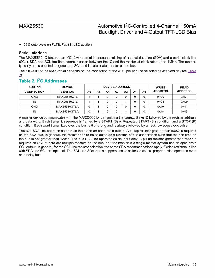
Serial InterfaceThe MAX25530 IC features an I2C, 2-wire serial interface consisting of a serial-data line (SDA) and a serial-clock line(SCL). SDA and SCL facilitate communication between the IC and the master at clock rates up to 1MHz. The master,typically a microcontroller, generates SCL and initiates data transfer on the bus.The Slave ID of the MAX25530 depends on the connection of the ADD pin and the selected device version (see Table2).
Table 2. I2C AddressesADD PIN
CONNECTIONDEVICE
VERSIONDEVICE ADDRESS WRITE
ADDRESSREAD
ADDRESSA6 A5 A4 A3 A2 A1 A0GND MAX25530GTL 1 1 0 0 0 0 0 0xC0 0xC1
IN MAX25530GTL 1 1 0 0 1 0 0 0xC8 0xC9GND MAX25530GTLA 0 1 0 0 0 0 0 0x40 0x41
IN MAX25530GTLA 0 1 0 0 1 0 0 0x48 0x49
A master device communicates with the MAX25530 by transmitting the correct Slave ID followed by the register addressand data word. Each transmit sequence is framed by a START (S) or Repeated START (Sr) condition, and a STOP (P)condition. Each word transmitted over the bus is 8 bits long and is always followed by an acknowledge clock pulse.The IC's SDA line operates as both an input and an open-drain output. A pullup resistor greater than 500Ω is requiredon the SDA bus. In general, the resistor has to be selected as a function of bus capacitance such that the rise time onthe bus is not greater than 120ns. The IC's SCL line operates as an input only. A pullup resistor greater than 500Ω isrequired on SCL if there are multiple masters on the bus, or if the master in a single-master system has an open-drainSCL output. In general, for the SCL-line resistor selection, the same SDA recommendations apply. Series resistors in linewith SDA and SCL are optional. The SCL and SDA inputs suppress noise spikes to assure proper device operation evenon a noisy bus.
MAX25530 Automotive I2C-Controlled 4-Channel 150mABacklight Driver and 4-Output TFT-LCD Bias
www.maximintegrated.com Maxim Integrated | 32
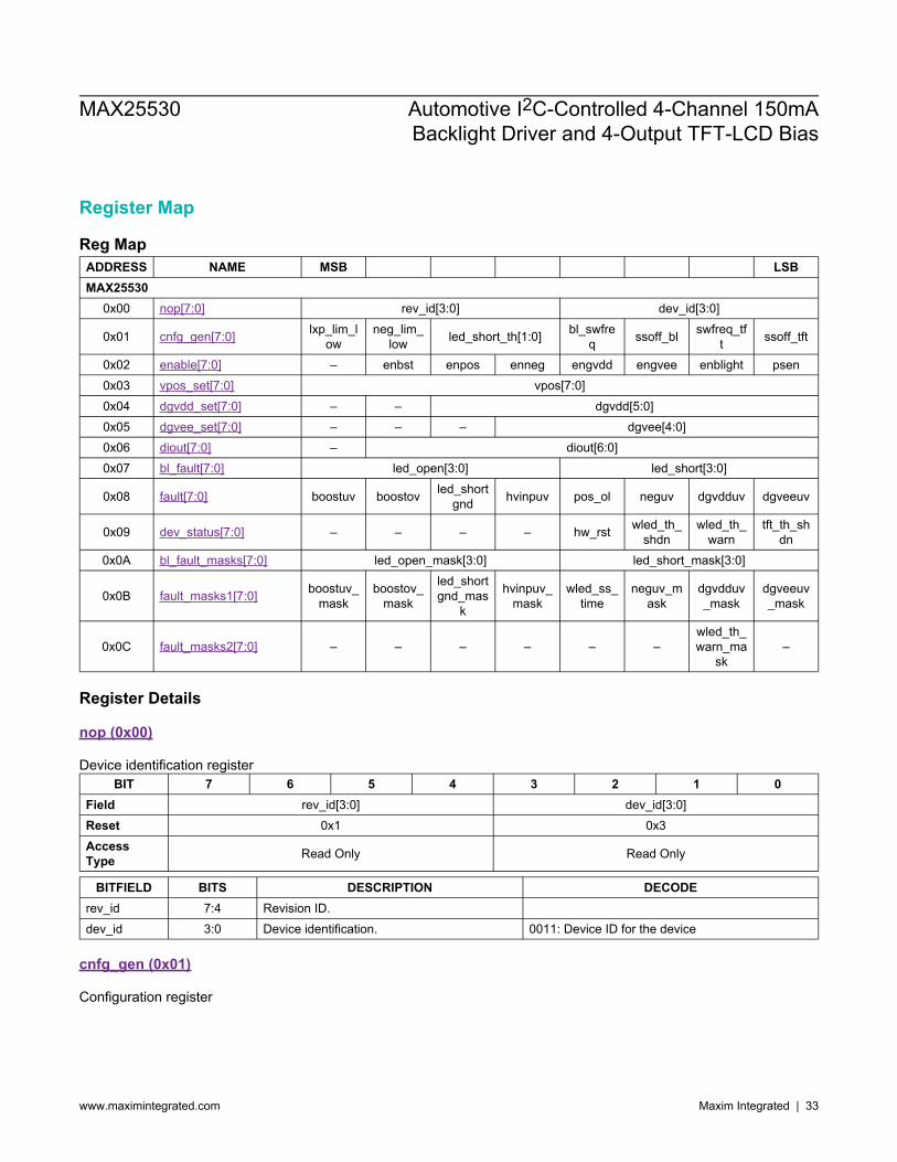
Register Map
Reg MapADDRESS NAME MSB LSBMAX25530
0x00 nop[7:0] rev_id[3:0] dev_id[3:0]
0x01 cnfg_gen[7:0] lxp_lim_low
neg_lim_low led_short_th[1:0] bl_swfre
q ssoff_bl swfreq_tft ssoff_tft
0x02 enable[7:0] – enbst enpos enneg engvdd engvee enblight psen0x03 vpos_set[7:0] vpos[7:0]0x04 dgvdd_set[7:0] – – dgvdd[5:0]0x05 dgvee_set[7:0] – – – dgvee[4:0]0x06 diout[7:0] – diout[6:0]0x07 bl_fault[7:0] led_open[3:0] led_short[3:0]
0x08 fault[7:0] boostuv boostov led_shortgnd hvinpuv pos_ol neguv dgvdduv dgveeuv
0x09 dev_status[7:0] – – – – hw_rst wled_th_shdn
wled_th_warn
tft_th_shdn
0x0A bl_fault_masks[7:0] led_open_mask[3:0] led_short_mask[3:0]
0x0B fault_masks1[7:0] boostuv_mask
boostov_mask
led_shortgnd_mas
k
hvinpuv_mask
wled_ss_time
neguv_mask
dgvdduv_mask
dgveeuv_mask
0x0C fault_masks2[7:0] – – – – – –wled_th_warn_ma
sk–
Register Details
nop (0x00)
Device identification registerBIT 7 6 5 4 3 2 1 0
Field rev_id[3:0] dev_id[3:0]Reset 0x1 0x3AccessType Read Only Read Only
BITFIELD BITS DESCRIPTION DECODErev_id 7:4 Revision ID.dev_id 3:0 Device identification. 0011: Device ID for the device
cnfg_gen (0x01)
Configuration register
MAX25530 Automotive I2C-Controlled 4-Channel 150mABacklight Driver and 4-Output TFT-LCD Bias
www.maximintegrated.com Maxim Integrated | 33
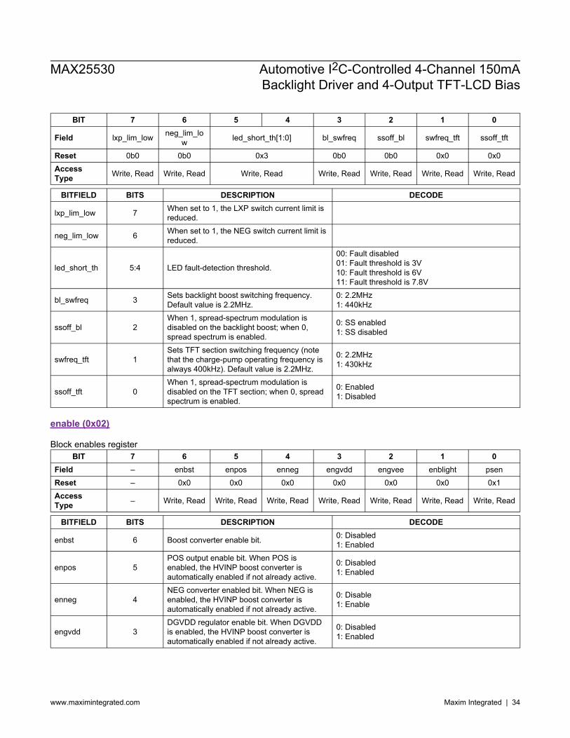
BIT 7 6 5 4 3 2 1 0
Field lxp_lim_low neg_lim_low led_short_th[1:0] bl_swfreq ssoff_bl swfreq_tft ssoff_tft
Reset 0b0 0b0 0x3 0b0 0b0 0x0 0x0AccessType Write, Read Write, Read Write, Read Write, Read Write, Read Write, Read Write, Read
BITFIELD BITS DESCRIPTION DECODE
lxp_lim_low 7 When set to 1, the LXP switch current limit isreduced.
neg_lim_low 6 When set to 1, the NEG switch current limit isreduced.
led_short_th 5:4 LED fault-detection threshold.
00: Fault disabled01: Fault threshold is 3V10: Fault threshold is 6V11: Fault threshold is 7.8V
bl_swfreq 3 Sets backlight boost switching frequency.Default value is 2.2MHz.
0: 2.2MHz1: 440kHz
ssoff_bl 2When 1, spread-spectrum modulation isdisabled on the backlight boost; when 0,spread spectrum is enabled.
0: SS enabled1: SS disabled
swfreq_tft 1Sets TFT section switching frequency (notethat the charge-pump operating frequency isalways 400kHz). Default value is 2.2MHz.
0: 2.2MHz1: 430kHz
ssoff_tft 0When 1, spread-spectrum modulation isdisabled on the TFT section; when 0, spreadspectrum is enabled.
0: Enabled1: Disabled
enable (0x02)
Block enables registerBIT 7 6 5 4 3 2 1 0
Field – enbst enpos enneg engvdd engvee enblight psenReset – 0x0 0x0 0x0 0x0 0x0 0x0 0x1AccessType – Write, Read Write, Read Write, Read Write, Read Write, Read Write, Read Write, Read
BITFIELD BITS DESCRIPTION DECODE
enbst 6 Boost converter enable bit. 0: Disabled1: Enabled
enpos 5POS output enable bit. When POS isenabled, the HVINP boost converter isautomatically enabled if not already active.
0: Disabled1: Enabled
enneg 4NEG converter enabled bit. When NEG isenabled, the HVINP boost converter isautomatically enabled if not already active.
0: Disable1: Enable
engvdd 3DGVDD regulator enable bit. When DGVDDis enabled, the HVINP boost converter isautomatically enabled if not already active.
0: Disabled1: Enabled
MAX25530 Automotive I2C-Controlled 4-Channel 150mABacklight Driver and 4-Output TFT-LCD Bias
www.maximintegrated.com Maxim Integrated | 34
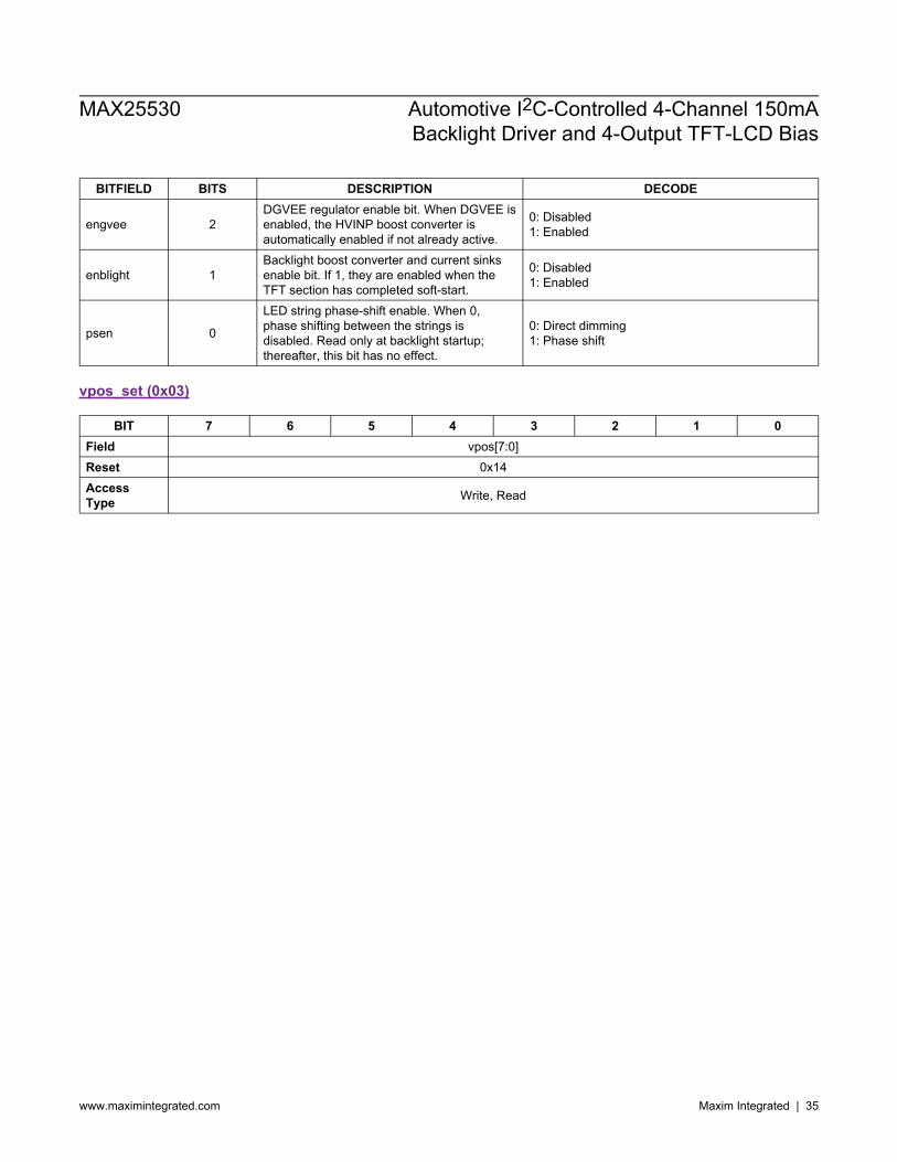
BITFIELD BITS DESCRIPTION DECODE
engvee 2DGVEE regulator enable bit. When DGVEE isenabled, the HVINP boost converter isautomatically enabled if not already active.
0: Disabled1: Enabled
enblight 1Backlight boost converter and current sinksenable bit. If 1, they are enabled when theTFT section has completed soft-start.
0: Disabled1: Enabled
psen 0
LED string phase-shift enable. When 0,phase shifting between the strings isdisabled. Read only at backlight startup;thereafter, this bit has no effect.
0: Direct dimming1: Phase shift
vpos_set (0x03)
BIT 7 6 5 4 3 2 1 0Field vpos[7:0]Reset 0x14AccessType Write, Read
MAX25530 Automotive I2C-Controlled 4-Channel 150mABacklight Driver and 4-Output TFT-LCD Bias
www.maximintegrated.com Maxim Integrated | 35
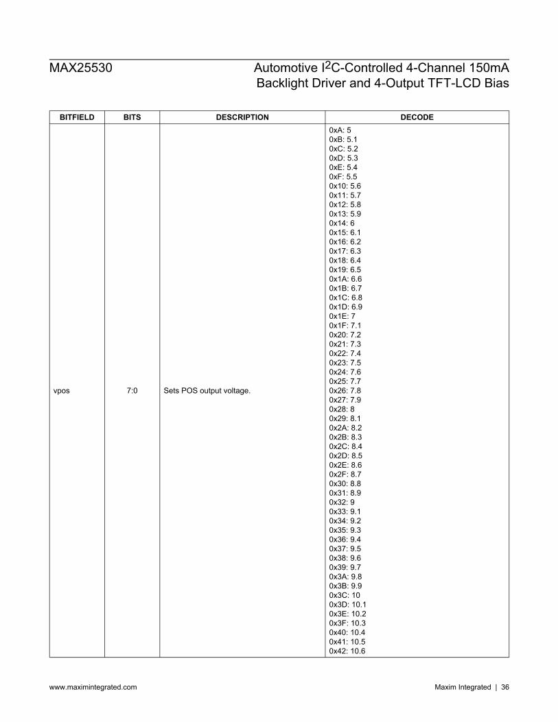
BITFIELD BITS DESCRIPTION DECODE
vpos 7:0 Sets POS output voltage.
0xA: 50xB: 5.10xC: 5.20xD: 5.30xE: 5.40xF: 5.50x10: 5.60x11: 5.70x12: 5.80x13: 5.90x14: 60x15: 6.10x16: 6.20x17: 6.30x18: 6.40x19: 6.50x1A: 6.60x1B: 6.70x1C: 6.80x1D: 6.90x1E: 70x1F: 7.10x20: 7.20x21: 7.30x22: 7.40x23: 7.50x24: 7.60x25: 7.70x26: 7.80x27: 7.90x28: 80x29: 8.10x2A: 8.20x2B: 8.30x2C: 8.40x2D: 8.50x2E: 8.60x2F: 8.70x30: 8.80x31: 8.90x32: 90x33: 9.10x34: 9.20x35: 9.30x36: 9.40x37: 9.50x38: 9.60x39: 9.70x3A: 9.80x3B: 9.90x3C: 100x3D: 10.10x3E: 10.20x3F: 10.30x40: 10.40x41: 10.50x42: 10.6
MAX25530 Automotive I2C-Controlled 4-Channel 150mABacklight Driver and 4-Output TFT-LCD Bias
www.maximintegrated.com Maxim Integrated | 36
BITFIELD BITS DESCRIPTION DECODE0x43: 10.70x44: 10.80x45: 10.90x46: 110x47: 11.10x48: 11.20x49: 11.30x4A: 11.40x4B: 11.50x4C: 11.60x4D: 11.70x4E: 11.80x4F: 11.90x50: 120x51: 12.10x52: 12.20x53: 12.30x54: 12.40x55: 12.50x56: 12.60x57: 12.70x58: 12.80x59: 12.90x5A: 130x5B: 13.10x5C: 13.20x5D: 13.30x5E: 13.40x5F: 13.50x60: 13.60x61: 13.70x62: 13.80x63: 13.90x64: 140x65: 14.10x66: 14.20x67: 14.30x68: 14.40x69: 14.50x6A: 14.60x6B: 14.70x6C: 14.80x6D: 14.90x6E: 150x6F: 15.10x70: 15.20x71: 15.30x72: 15.40x73: 15.50x74: 15.60x75: 15.70x76: 15.80x77: 15.90x78: 160x79: 16.10x7A: 16.20x7B: 16.3
MAX25530 Automotive I2C-Controlled 4-Channel 150mABacklight Driver and 4-Output TFT-LCD Bias
www.maximintegrated.com Maxim Integrated | 37
BITFIELD BITS DESCRIPTION DECODE0x7C: 16.40x7D: 16.50x7E: 16.60x7F: 16.70x80: 16.80x81: 16.90x82: 170x83: 17.10x84: 17.20x85: 17.30x86: 17.40x87: 17.50x88: 17.60x89: 17.70x8A: 17.80x8B: 17.90x8C: 180x8D-0xFF: 18
dgvdd_set (0x04)
BIT 7 6 5 4 3 2 1 0Field – – dgvdd[5:0]Reset – – 0x0AccessType – – Write, Read
MAX25530 Automotive I2C-Controlled 4-Channel 150mABacklight Driver and 4-Output TFT-LCD Bias
www.maximintegrated.com Maxim Integrated | 38
BITFIELD BITS DESCRIPTION DECODE
dgvdd 5:0 Sets DGVDD output voltage.
0x0: 80x1: 8.50x2: 90x3: 9.50x4: 100x5: 10.50x6: 110x7: 11.50x8: 120x9: 12.50xA: 130xB: 13.50xC: 140xD: 14.50xE: 150xF: 15.50x10: 160x11: 16.50x12: 170x13: 17.50x14: 180x15: 18.50x16: 190x17: 19.50x18: 200x19: 20.50x1A: 210x1B: 21.50x1C: 220x1D: 22.50x1E: 230x1F: 23.50x20: 240x21: 24.50x22: 250x23: 25.50x24: 260x25: 26.50x26: 270x27: 27.50x28: 280x29- 0x3F: Unused
dgvee_set (0x05)
BIT 7 6 5 4 3 2 1 0Field – – – dgvee[4:0]Reset – – – 0x0AccessType – – – Write, Read
MAX25530 Automotive I2C-Controlled 4-Channel 150mABacklight Driver and 4-Output TFT-LCD Bias
www.maximintegrated.com Maxim Integrated | 39
BITFIELD BITS DESCRIPTION DECODE
dgvee 4:0 Sets DGVEE output voltage.
0x0: -60x1: -6.50x2: -70x3: -7.50x4: -80x5: -8.50x6: -90x7: -9.50x8: -100x9: -10.50xA: -110xB: -11.50xC: -120xD: -12.50xE: -130xF: -13.50x10: -140x11: -14.50x12: -150x13: -15.50x14: -160x15: -16.50x16: -170x17: -17.50x18: -180x19: -18.50x1A: -190x1B: -19.50x1C: -200x1D: -20.50x1E: -210x1F: -21.5
diout (0x06)
BIT 7 6 5 4 3 2 1 0Field – diout[6:0]Reset – 0x7FAccessType – Write, Read
MAX25530 Automotive I2C-Controlled 4-Channel 150mABacklight Driver and 4-Output TFT-LCD Bias
www.maximintegrated.com Maxim Integrated | 40
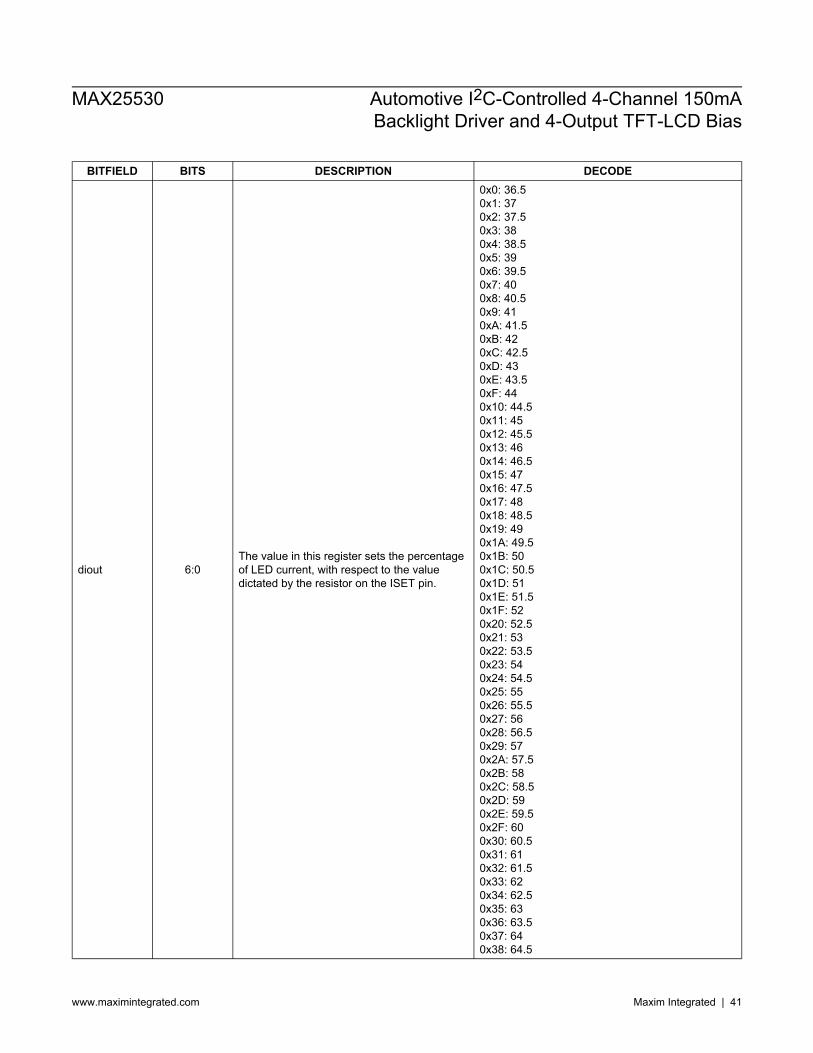
BITFIELD BITS DESCRIPTION DECODE
diout 6:0The value in this register sets the percentageof LED current, with respect to the valuedictated by the resistor on the ISET pin.
0x0: 36.50x1: 370x2: 37.50x3: 380x4: 38.50x5: 390x6: 39.50x7: 400x8: 40.50x9: 410xA: 41.50xB: 420xC: 42.50xD: 430xE: 43.50xF: 440x10: 44.50x11: 450x12: 45.50x13: 460x14: 46.50x15: 470x16: 47.50x17: 480x18: 48.50x19: 490x1A: 49.50x1B: 500x1C: 50.50x1D: 510x1E: 51.50x1F: 520x20: 52.50x21: 530x22: 53.50x23: 540x24: 54.50x25: 550x26: 55.50x27: 560x28: 56.50x29: 570x2A: 57.50x2B: 580x2C: 58.50x2D: 590x2E: 59.50x2F: 600x30: 60.50x31: 610x32: 61.50x33: 620x34: 62.50x35: 630x36: 63.50x37: 640x38: 64.5
MAX25530 Automotive I2C-Controlled 4-Channel 150mABacklight Driver and 4-Output TFT-LCD Bias
www.maximintegrated.com Maxim Integrated | 41
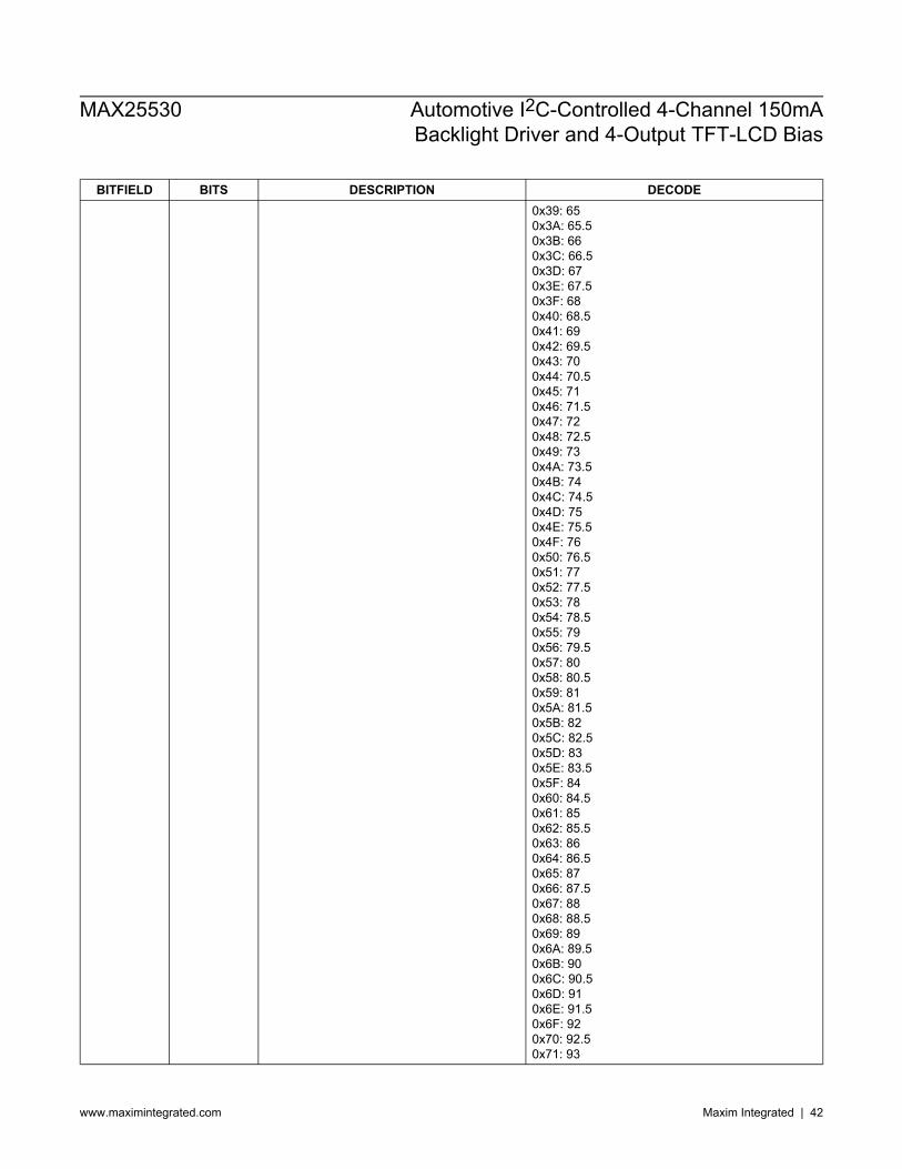
BITFIELD BITS DESCRIPTION DECODE0x39: 650x3A: 65.50x3B: 660x3C: 66.50x3D: 670x3E: 67.50x3F: 680x40: 68.50x41: 690x42: 69.50x43: 700x44: 70.50x45: 710x46: 71.50x47: 720x48: 72.50x49: 730x4A: 73.50x4B: 740x4C: 74.50x4D: 750x4E: 75.50x4F: 760x50: 76.50x51: 770x52: 77.50x53: 780x54: 78.50x55: 790x56: 79.50x57: 800x58: 80.50x59: 810x5A: 81.50x5B: 820x5C: 82.50x5D: 830x5E: 83.50x5F: 840x60: 84.50x61: 850x62: 85.50x63: 860x64: 86.50x65: 870x66: 87.50x67: 880x68: 88.50x69: 890x6A: 89.50x6B: 900x6C: 90.50x6D: 910x6E: 91.50x6F: 920x70: 92.50x71: 93
MAX25530 Automotive I2C-Controlled 4-Channel 150mABacklight Driver and 4-Output TFT-LCD Bias
www.maximintegrated.com Maxim Integrated | 42
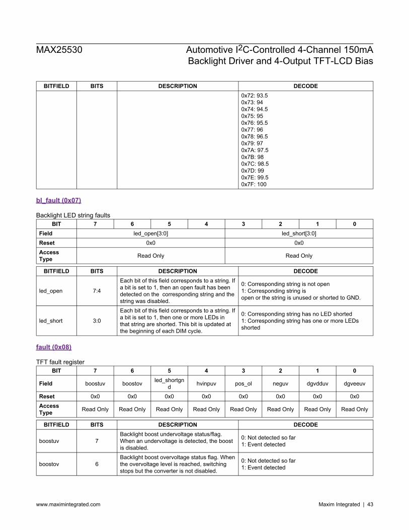
BITFIELD BITS DESCRIPTION DECODE0x72: 93.50x73: 940x74: 94.50x75: 950x76: 95.50x77: 960x78: 96.50x79: 970x7A: 97.50x7B: 980x7C: 98.50x7D: 990x7E: 99.50x7F: 100
bl_fault (0x07)
Backlight LED string faultsBIT 7 6 5 4 3 2 1 0
Field led_open[3:0] led_short[3:0]Reset 0x0 0x0AccessType Read Only Read Only
BITFIELD BITS DESCRIPTION DECODE
led_open 7:4
Each bit of this field corresponds to a string. Ifa bit is set to 1, then an open fault has beendetected on the corresponding string and thestring was disabled.
0: Corresponding string is not open1: Corresponding string isopen or the string is unused or shorted to GND.
led_short 3:0
Each bit of this field corresponds to a string. Ifa bit is set to 1, then one or more LEDs inthat string are shorted. This bit is updated atthe beginning of each DIM cycle.
0: Corresponding string has no LED shorted1: Corresponding string has one or more LEDsshorted
fault (0x08)
TFT fault registerBIT 7 6 5 4 3 2 1 0
Field boostuv boostov led_shortgnd hvinpuv pos_ol neguv dgvdduv dgveeuv
Reset 0x0 0x0 0x0 0x0 0x0 0x0 0x0 0x0AccessType Read Only Read Only Read Only Read Only Read Only Read Only Read Only Read Only
BITFIELD BITS DESCRIPTION DECODE
boostuv 7Backlight boost undervoltage status/flag.When an undervoltage is detected, the boostis disabled.
0: Not detected so far1: Event detected
boostov 6Backlight boost overvoltage status flag. Whenthe overvoltage level is reached, switchingstops but the converter is not disabled.
0: Not detected so far1: Event detected
MAX25530 Automotive I2C-Controlled 4-Channel 150mABacklight Driver and 4-Output TFT-LCD Bias
www.maximintegrated.com Maxim Integrated | 43
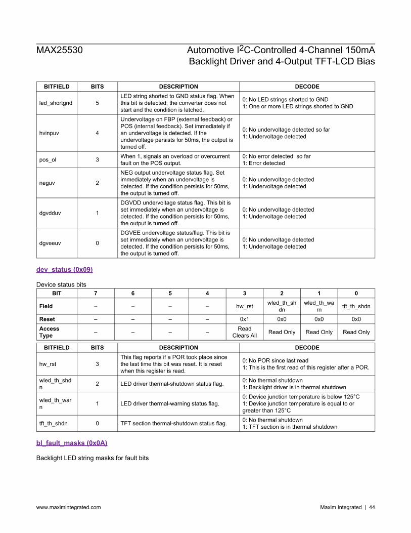
BITFIELD BITS DESCRIPTION DECODE
led_shortgnd 5LED string shorted to GND status flag. Whenthis bit is detected, the converter does notstart and the condition is latched.
0: No LED strings shorted to GND1: One or more LED strings shorted to GND
hvinpuv 4
Undervoltage on FBP (external feedback) orPOS (internal feedback). Set immediately ifan undervoltage is detected. If theundervoltage persists for 50ms, the output isturned off.
0: No undervoltage detected so far1: Undervoltage detected
pos_ol 3 When 1, signals an overload or overcurrentfault on the POS output.
0: No error detected so far1: Error detected
neguv 2
NEG output undervoltage status flag. Setimmediately when an undervoltage isdetected. If the condition persists for 50ms,the output is turned off.
0: No undervoltage detected1: Undervoltage detected
dgvdduv 1
DGVDD undervoltage status flag. This bit isset immediately when an undervoltage isdetected. If the condition persists for 50ms,the output is turned off.
0: No undervoltage detected1: Undervoltage detected
dgveeuv 0
DGVEE undervoltage status/flag. This bit isset immediately when an undervoltage isdetected. If the condition persists for 50ms,the output is turned off.
0: No undervoltage detected1: Undervoltage detected
dev_status (0x09)
Device status bitsBIT 7 6 5 4 3 2 1 0
Field – – – – hw_rst wled_th_shdn
wled_th_warn tft_th_shdn
Reset – – – – 0x1 0x0 0x0 0x0AccessType – – – – Read
Clears All Read Only Read Only Read Only
BITFIELD BITS DESCRIPTION DECODE
hw_rst 3This flag reports if a POR took place sincethe last time this bit was reset. It is resetwhen this register is read.
0: No POR since last read1: This is the first read of this register after a POR.
wled_th_shdn 2 LED driver thermal-shutdown status flag. 0: No thermal shutdown
1: Backlight driver is in thermal shutdown
wled_th_warn 1 LED driver thermal-warning status flag.
0: Device junction temperature is below 125°C1: Device junction temperature is equal to orgreater than 125°C
tft_th_shdn 0 TFT section thermal-shutdown status flag. 0: No thermal shutdown1: TFT section is in thermal shutdown
bl_fault_masks (0x0A)
Backlight LED string masks for fault bits
MAX25530 Automotive I2C-Controlled 4-Channel 150mABacklight Driver and 4-Output TFT-LCD Bias
www.maximintegrated.com Maxim Integrated | 44
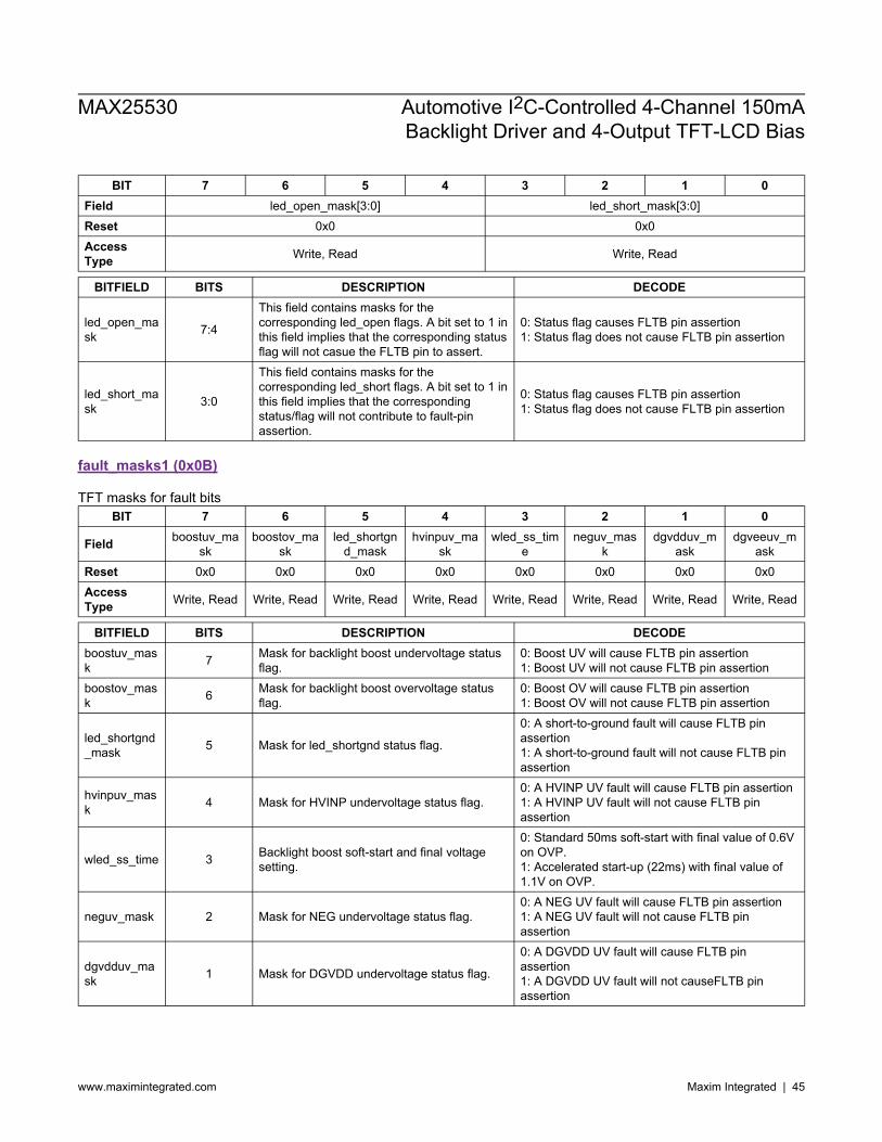
BIT 7 6 5 4 3 2 1 0Field led_open_mask[3:0] led_short_mask[3:0]Reset 0x0 0x0AccessType Write, Read Write, Read
BITFIELD BITS DESCRIPTION DECODE
led_open_mask 7:4
This field contains masks for thecorresponding led_open flags. A bit set to 1 inthis field implies that the corresponding statusflag will not casue the FLTB pin to assert.
0: Status flag causes FLTB pin assertion1: Status flag does not cause FLTB pin assertion
led_short_mask 3:0
This field contains masks for thecorresponding led_short flags. A bit set to 1 inthis field implies that the correspondingstatus/flag will not contribute to fault-pinassertion.
0: Status flag causes FLTB pin assertion1: Status flag does not cause FLTB pin assertion
fault_masks1 (0x0B)
TFT masks for fault bitsBIT 7 6 5 4 3 2 1 0
Field boostuv_mask
boostov_mask
led_shortgnd_mask
hvinpuv_mask
wled_ss_time
neguv_mask
dgvdduv_mask
dgveeuv_mask
Reset 0x0 0x0 0x0 0x0 0x0 0x0 0x0 0x0AccessType Write, Read Write, Read Write, Read Write, Read Write, Read Write, Read Write, Read Write, Read
BITFIELD BITS DESCRIPTION DECODEboostuv_mask 7 Mask for backlight boost undervoltage status
flag.0: Boost UV will cause FLTB pin assertion1: Boost UV will not cause FLTB pin assertion
boostov_mask 6 Mask for backlight boost overvoltage status
flag.0: Boost OV will cause FLTB pin assertion1: Boost OV will not cause FLTB pin assertion
led_shortgnd_mask 5 Mask for led_shortgnd status flag.
0: A short-to-ground fault will cause FLTB pinassertion1: A short-to-ground fault will not cause FLTB pinassertion
hvinpuv_mask 4 Mask for HVINP undervoltage status flag.
0: A HVINP UV fault will cause FLTB pin assertion1: A HVINP UV fault will not cause FLTB pinassertion
wled_ss_time 3 Backlight boost soft-start and final voltagesetting.
0: Standard 50ms soft-start with final value of 0.6Von OVP.1: Accelerated start-up (22ms) with final value of1.1V on OVP.
neguv_mask 2 Mask for NEG undervoltage status flag.0: A NEG UV fault will cause FLTB pin assertion1: A NEG UV fault will not cause FLTB pinassertion
dgvdduv_mask 1 Mask for DGVDD undervoltage status flag.
0: A DGVDD UV fault will cause FLTB pinassertion1: A DGVDD UV fault will not causeFLTB pinassertion
MAX25530 Automotive I2C-Controlled 4-Channel 150mABacklight Driver and 4-Output TFT-LCD Bias
www.maximintegrated.com Maxim Integrated | 45
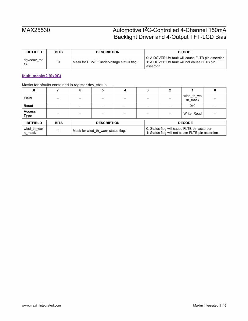
BITFIELD BITS DESCRIPTION DECODE
dgveeuv_mask 0 Mask for DGVEE undervoltage status flag.
0: A DGVEE UV fault will cause FLTB pin assertion1: A DGVEE UV fault will not cause FLTB pinassertion
fault_masks2 (0x0C)
Masks for ofaults contained in register dev_statusBIT 7 6 5 4 3 2 1 0
Field – – – – – – wled_th_warn_mask –
Reset – – – – – – 0x0 –AccessType – – – – – – Write, Read –
BITFIELD BITS DESCRIPTION DECODEwled_th_warn_mask 1 Mask for wled_th_warn status flag. 0: Status flag will cause FLTB pin assertion
1: Status flag will not cause FLTB pin assertion
MAX25530 Automotive I2C-Controlled 4-Channel 150mABacklight Driver and 4-Output TFT-LCD Bias
www.maximintegrated.com Maxim Integrated | 46
Applications Information
TFT Power Section
Boost Converter
Boost Converter Inductor SelectionSelect the value of the boost inductor using the following table:
fSW VPOS < 10V VPOS > 10V430kHz 4.7μH 10μH2.2MHz 1μH 2.2μH
The inductor’s saturation rating must exceed the maximum current limit of 1.7A or 0.74A, depending on the setting of thelxp_lim_low bit in the cnfg_gen (0x01) register.
Boost Output-Filter Capacitor SelectionThe primary criterion for selecting the output-filter capacitor is low effective series resistance (ESR). The product of thepeak inductor current and the output filter capacitor’s ESR determine the amplitude of the high-frequency ripple seen onthe output voltage. For stability, the boost output-filter capacitor should have a value of 10μF or greater.To avoid a large drop on HVINP when POS is enabled, the capacitance on the HVINP node should be at least threetimes larger than that on POS.
Setting the POS VoltageIn stand-alone mode, the POS output voltage is set by connecting FBP to a resistive voltage divider between HVINP andGND. Select the lower feedback resistor value and calculate the upper resistor value using the following formula.Equation 9:
RUPPER =(VHVINP − 1.25) × RLOWER
1.25
In I2C mode, the POS output is set by writing an 8-bit value to the vpos_set (0x03) register.The NEG converter outputs a negative voltage whose absolute value is the same as POS. The most negative voltagethe NEG can output is -7V.
NEG Inverting Regulator
NEG Regulator Inductor SelectionSelect the inductor value for the NEG regulator based on the switching frequency: at 430kHz use 10μH and at 2.2MHzuse 2.2μH.The inductor's saturation current rating must exceed the maximum current-limit setting of 1.2A or 0.6A, depending on thesetting of the neg_lim_low bit in the cnfg_gen (0x01) register.
NEG External Diode SelectionSelect a diode with a peak current rating of at least the selected LXN current limit (1.8A or 1.1A) for use with the NEGoutput. The diode breakdown-voltage rating should exceed the sum of the maximum INN voltage and the absolute valueof the NEG voltage. A Schottky diode improves the overall efficiency of the converter.
NEG Output Capacitor SelectionThe primary criterion for selecting the output filter capacitor is low ESR and capacitance value, as the NEG capacitorprovides the load current when the internal switch is on. The voltage ripple on the NEG output has two components:
MAX25530 Automotive I2C-Controlled 4-Channel 150mABacklight Driver and 4-Output TFT-LCD Bias
www.maximintegrated.com Maxim Integrated | 47

Ripple due to ESR, which is the product of the peak inductor current and the output filter capacitor’s ESR Ripple due to bulk capacitance that can be determined as follows:Equation 10:
ΔVBULK =INEG × D
fSWCNEG
For stability, the NEG output capacitor should have a value of 10μF or greater.
Setting the DGVDD and DGVEE Output VoltagesFor most applications, a single charge-pump stage is sufficient for both the positive and negative charge pumps. In thecase of DGVDD, the maximum output voltage is then twice the HVINP voltage. For DGVEE, the most negative voltageis -VHVINP. If necessary, add further stages while maintaining the DGVDD and DGVEE voltages within their permittedoperating ranges.The DGVDD output voltage is set in stand-alone mode with a resistor-divider from DGVDD to GND, with its centerconnected to the FBPG pin. After a value for RLOWER is selected, RUPPER can be calculated using the following formula.Equation 11:
RUPPER =(DGVDD − 1.25) × RLOWER
1.25
The DGVEE output voltage is set by connecting a resistor-divider from REF to DGVEE, with its center connected toFBNG. The control loop forces FBNG to 0V. Select the resistor connected to REF (RREF) so that less than 100μA isdrawn from REF (i.e., the value of RREF shall be greater than 12.5kΩ). After selecting RREF, calculate RDGVEE usingEquation 12.Equation 12:
RDGVEE =RREF × |DGVEE|
1.25
In I2C mode, the DGVDD and DGVEE voltages are set by writing a 6-bit value to the dgvdd_set (0x04) register and a5-bit value to the dgvee_set (0x05) register, respectively.
LED Driver Section
DC-DC Converter for LED DriverTwo different converter topologies are possible with the DC-DC controller in the device, which has the ground-referencedoutputs necessary to use the constant-current sink drivers. If the LED string forward voltage is always higher than theinput supply voltage range, use the boost-converter topology. If the LED string forward voltage falls within the supply-voltage range, use the SEPIC topology.Note that the boost converter topology provides the highest efficiency.
Power-Circuit DesignFirst select a converter topology based on the above factors. Determine the required input supply-voltage range, themaximum voltage needed to drive the LED strings, including the worst-case 1V across the constant LED current sink(VLED), and the total output current needed to drive the LED strings (ILED) as shown below.Equation 13:ILED = ISTRING × NSTRING
where ISTRING is the LED current per string in amperes and NSTRING is the number of strings used. Calculate themaximum duty cycle (DMAX) using the following equations:Equation 14 (for the boost configuration):
MAX25530 Automotive I2C-Controlled 4-Channel 150mABacklight Driver and 4-Output TFT-LCD Bias
www.maximintegrated.com Maxim Integrated | 48
DMAX =(VLED + VD1 − VIN_MIN)
(VLED + VD1 − VDS − 0.42)Equation 15 (for the SEPIC configuration):
DMAX =(VLED + VD1)
(VIN_MIN − VDS − 0.42 + VLED + VD1)where VD1 is the forward drop of the rectifier diode in volts (approximately 0.6V), VIN_MIN is the minimum input supplyvoltage in volts, VDS is the drain-to-source voltage of the external MOSFET in volts when it is on, and 0.42V is the peakcurrent-sense voltage. Initially, use an approximate value of 0.2V for VDS to calculate DMAX. Calculate a more accuratevalue of DMAX after the power MOSFET is selected based on the maximum inductor current.
Boost ConfigurationThe average inductor current varies with the line voltage, and the maximum average current occurs at the lowest linevoltage. For the boost converter, the average inductor current is equal to the input current. Select the maximum peak-to-peak ripple on the inductor current (ΔIL). The recommended peak-to-peak ripple is 60% of the average inductor current.Use the following equations to calculate the maximum average inductor current (ILAVG) and peak inductor current (ILP)in amperes.Equation 16:
ILAVG =ILED
1 − DMAX
Allowing the peak-to-peak inductor ripple ΔIL to be ±30% of the average inductor current:Equation 17:ΔIL = ILAVG × 0.3 × 2
and
ILP = ILAVG +ΔIL2
Calculate the minimum inductance value (LMIN), in henries with the inductor-current ripple set to the maximum value.Equation 18:
LMIN =(VIN_MIN − VDS − 0.42) × DMAX
fSW × ΔIL
where 0.42V is the peak current-sense voltage. Choose an inductor that has a minimum inductance greater than thecalculated LMIN and current rating greater than ILP. The recommended saturation current limit of the selected inductor is10% higher than the inductor peak current for boost configuration.
SEPIC ConfigurationPower-circuit design for the SEPIC configuration is very similar to a conventional design, with the output voltagereferenced to the input supply voltage. For SEPIC, the output is referenced to ground and the inductor is split into twoparts (see Typical Application Circuits). One of the inductors (L2) has the LED current as the average current, and theother inductor (L1) has the input current as its average current. Use the following equations to calculate the averageinductor currents (IL1AVG, IL2AVG) and peak inductor currents (IL1P, IL2P) in amperes:Equation 19:
IL1AVG =ILED × DMAX × 1.1
1 − DMAX
The factor 1.1 provides a 10% margin to account for the converter losses:
MAX25530 Automotive I2C-Controlled 4-Channel 150mABacklight Driver and 4-Output TFT-LCD Bias
www.maximintegrated.com Maxim Integrated | 49
Equation 20:IL2AVG = ILED
Assuming the peak-to-peak inductor ripple ΔIL is ±30% of the average inductor current:Equation 21:ΔIL1 = IL1AVG × 0.3 × 2
and
IL1P = IL1AVG +ΔIL1
2
ΔIL2 = IL2AVG × 0.3 × 2
and
IL2P = IL2AVG +ΔIL2
2
Calculate the minimum inductance values L1MIN and L2MIN in henries with the inductor current ripples set to themaximum value as follows:Equation 22:
L1MIN =(VIN_MIN − VDS − 0.42) × DMAX
fSW × ΔIL1
L2MIN =(VIN_MIN − VDS − 0.42) × DMAX
fSW × ΔIL2
where 0.42V is the peak current-sense voltage. Choose inductors that have a minimum inductance greater than thecalculated L1MIN and L2MIN, and current ratings greater than IL1P and IL2P, respectively. The recommended saturationcurrent limit of the selected inductor is 10% higher than the inductor peak current.For simplifying further calculations, consider L1 and L2 as a single inductor with L1/L2 connected in parallel. Thecombined inductance value and current is calculated as follows:Equation 23:
LMIN =L1MIN × L2MINL1MIN + L2MIN
andILAVG = IL1AVG + IL2AVG
where ILAVG represents the total average current through both the inductors, connected together for SEPICconfiguration. Use these values in the calculations for the SEPIC configuration in the following sections.Select coupling capacitor CS so that the peak-to-peak ripple on it is less than 2% of the minimum input supply voltage.This ensures that the second-order effects created by the series resonant circuit comprising L1, CS, and L2 do not affectthe normal operation of the converter. Use the following equation to calculate the minimum value of CS.Equation 24:
CS ≥ILED × DMAX
VIN_MIN × 0.02 × fSW
where CS is the minimum value of the coupling capacitor in farads, ILED is the LED current in amperes, and the factor0.02 accounts for 2% ripple.
Current-Sense Resistor and Slope CompensationThe MAX25530 backlight boost generates a current ramp for slope compensation. This ramp current is in sync with the
MAX25530 Automotive I2C-Controlled 4-Channel 150mABacklight Driver and 4-Output TFT-LCD Bias
www.maximintegrated.com Maxim Integrated | 50
switching frequency, starting from zero at the beginning of every clock cycle and rising linearly to reach 50μA at the endof the clock cycle. The slope-compensating resistor (RSC) is connected between the CS input and the source of theexternal MOSFET. This adds a programmable ramp voltage to the CS input voltage to provide slope compensation.Use the following equation to calculate the value of slope-compensation resistance (RSC):Equation 25: (for boost configuration):
RSC =(VLED − 2 × VIN_MIN) × RCS × 3
LMIN × 50μA × fSW × 4
Equation 26: (for SEPIC and coupled-inductor configurations):
RSC =(VLED − VIN_MIN) × RCS × 3
LMIN × 50μA × fSW × 4
where VLED and VIN_MIN are in volts, RSC and RCS are in ohms, LMIN is in henries, and fSW is in hertz. The value ofthe switch current-sense resistor (RCS) can be calculated as follows:Equation 27: (for the boost configuration):
RCS =4 × LMIN × fSW × 0.39 × 0.9
ILP × 4 × LMIN × fSW + DMAX × (VLED − 2 × VIN_MIN) × 3
Equation 28: (for SEPIC and coupled-inductor configurations):
RCS =4 × LMIN × fSW × 0.39 × 0.9
ILP × 4 × LMIN × fSW + DMAX × (VLED − VIN_MIN) × 3
where 0.39 is the minimum value of the peak current-sense threshold. The current-sense threshold also includes theslope-compensation component. The minimum current-sense threshold of 0.4 is multiplied by 0.9 to take tolerances intoaccount.
Output Capacitor SelectionFor all converter topologies, the output capacitor supplies the load current when the main switch is on. The function ofthe output capacitor is to reduce the converter output ripple to acceptable levels. The entire output-voltage ripple appearsacross the constant-current sink outputs because the LED string voltages are stable due to the constant current. For theMAX25530, limit the peak-to-peak output-voltage ripple to 200mV to get stable output current.The ESR, ESL, and bulk capacitance of the output capacitor contribute to the output ripple. In most applications, usinglow-ESR ceramic capacitors can dramatically reduce the output ESR and ESL effects, connecting multiple ceramiccapacitors in parallel to achieve the required bulk capacitance. To minimize audible noise during PWM dimming however,it may be desirable to limit the use of ceramic capacitors on the boost output. In such cases, an additional electrolytic ortantalum capacitor can provide the majority of the bulk capacitance.
External Switching-MOSFET SelectionThe external switching MOSFET should have a voltage rating sufficient to withstand the maximum boost output voltage,together with the rectifier diode drop and any possible overshoot due to ringing caused by parasitic inductance andcapacitance. The recommended MOSFET VDS voltage rating is 30% higher than the sum of the maximum output voltageand the rectifier diode drop.The continuous-drain current rating of the MOSFET (ID), when the case temperature is at the maximum operatingambient temperature, should be greater than that calculated below.Equation 29:
IDRMS = (√ILAVG2 × DMAX) × 1.3
The MOSFET dissipates power due to both switching losses and conduction losses. Use the following equation tocalculate the conduction losses in the MOSFET.
MAX25530 Automotive I2C-Controlled 4-Channel 150mABacklight Driver and 4-Output TFT-LCD Bias
www.maximintegrated.com Maxim Integrated | 51

Equation 30:
PCOND = IL2AVG × DMAX × RDS(ON)
where RDS(ON) is the on-state drain-to-source resistance of the MOSFET. Use the following equation to calculate theswitching losses in the MOSFET.Equation 31:
PSW =ILAVG × VLED
2 × CGD × fSW2 × ( 1
IGON+ 1
IGOFF )where IGON and IGOFF are the gate currents of the MOSFET in amperes when it is turned on and turned off, respectively.CGD is the gate-to-drain MOSFET capacitance in farads.
Rectifier Diode SelectionUsing a Schottky rectifier diode produces less forward drop and puts the least burden on the MOSFET during reverserecovery. A diode with considerable reverse-recovery time increases the MOSFET switching loss. Select a Schottkydiode with a voltage rating 20% higher than the maximum boost-converter output voltage and current rating greater thanthat calculated in the following equation.Equation 32:
ID = ILAVG × (1 − DMAX) × 1.2
Feedback CompensationDuring normal operation, the feedback control loop regulates the minimum OUT_ voltage to fall within the windowcomparator limits of 0.8V and 1.1V when LED string currents are enabled during PWM dimming. When LED currentsare off during PWM dimming, the control loop turns off the converter and stores the steady-state condition in the formof capacitor voltages, primarily the output filter-capacitor voltage and compensation-capacitor voltage. When the PWMdimming pulses are less than 24 switching-clock cycles, the feedback loop regulates the converter output voltage to 95%of the OVP threshold.The worst-case condition for the feedback loop is when the LED driver is in normal mode regulating the minimum OUT_voltage. The switching converter small-signal transfer function has a right-half plane (RHP) zero for boost configurationif the inductor current is in continuous-conduction mode. The RHP zero adds a 20dB/decade gain and a 90° phase lag,which is difficult to compensate.The worst-case RHP zero frequency (fZRHP) is calculated as follows:Equation 33 (for boost configuration):
fZRHP =VLED × (1 − DMAX)2
2π × L × ILED
Equation 34 (for SEPIC configuration):
fZRHP =VLED × (1 − DMAX)2
2π × L × ILED × DMAX
where fZRHP is in hertz, VLED is in volts, L is the inductance value of L1 in henries, and ILED is in amperes. A simple wayto avoid this zero is to roll off the loop gain to 0dB at a frequency less than 1/5 of the RHP zero frequency with a -20dB/decade slope.The switching converter small-signal transfer function also has an output pole. The effective output impedance, togetherwith the output filter capacitance, determines the output pole frequency (fP1), calculated as follows:Equation 35 (for boost configuration):
MAX25530 Automotive I2C-Controlled 4-Channel 150mABacklight Driver and 4-Output TFT-LCD Bias
www.maximintegrated.com Maxim Integrated | 52

fP1 =ILED
2π × VLED × COUT
Equation 36 (for SEPIC configuration):
fP1 =ILED × DMAX
2π × VLED × COUT
where fP1 is in hertz, VLED is in volts, ILED is in amperes, and COUT is in farads. Compensation components (RCOMPand CCOMP) perform two functions: CCOMP introduces a low-frequency pole that presents a -20dB/ decade slope tothe loop gain, and RCOMP flattens the gain of the error amplifier for frequencies above the zero formed by RCOMP andCCOMP. For compensation, this zero is placed at the output pole frequency (fP1), so it provides a -20dB/decade slope forfrequencies above fP1 to the combined modulator and compensator response.The value of RCOMP needed to fix the total loop gain at fP1, so the total loop gain crosses 0dB with -20dB/decade slopeat 1/5 the RHP zero frequency, is calculated as follows.Equation 37 (for boost configuration):
RCOMP =fZRHP × RCS × ILED
5 × fP1 × GMCOMP × VLED × (1 − DMAX)Equation 38 (for SEPIC configuration):
RCOMP =fZRHP × RCS × ILED × DMAX
5 × fP1 × GMCOMP × VLED × (1 − DMAX)where RCOMP is the compensation resistor in ohms, fZRHP and fP2 are in hertz, RCS is the switch current-sense resistorin ohms, and GMCOMP is the transconductance of the error amplifier (700μS).The value of CCOMP is calculated as follows.Equation 39:
CCOMP = 12π × RCOMP × fZ1
where fZ1 is the compensation zero placed at 1/5 of the crossover frequency that is, in turn, set at 1/5 of the fZRHP. Ifthe output capacitors do not have low ESR, the ESR zero frequency may fall within the 0dB crossover frequency. Anadditional pole may be required to cancel out this pole placed at the same frequency. This is usually implemented byconnecting a capacitor in parallel with CCOMP and RCOMP.
MAX25530 Automotive I2C-Controlled 4-Channel 150mABacklight Driver and 4-Output TFT-LCD Bias
www.maximintegrated.com Maxim Integrated | 53
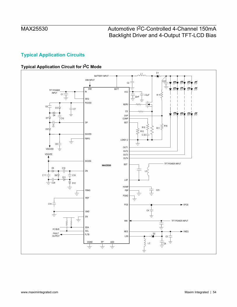
Typical Application Circuits
Typical Application Circuit for I2C Mode
MAX25530MAX25530
BATTVCC
NDRV
LGND1,2
COMP
CS
OVP
ISET
DIM
OUT1
LXP
FBP
INN
HVINP
POS
NEG
LXN
EP
EN
GND
SEQ
DN
DP
PGVDD
IN
DGVEE
DGVDD
FBPG
FBNG
REF
C1
BATTERY INPUT
C2C21
R15 R11R12
DIM INPUT
C23
C4
C5
C6L 2
D2
VPOS
VNEGFAULT
OUTPUT
TFT POWERINPUT
C7
C10
C9
VDGVDD
VDGVEE
C10
C19
C14
C 11
C20
D 3
D 9
D5
D11D6
D12
L3
R16
D4
C8
C4
D7
TFT POWER INPUT
FLTB
TFT POWER INPUT
R 17
C 22
L 1 D 1
OUT2OUT3OUT4
DGND ADD
PGND
SDASCL
I2C BUS
BST
2.2mF22nF
MAX25530 Automotive I2C-Controlled 4-Channel 150mABacklight Driver and 4-Output TFT-LCD Bias
www.maximintegrated.com Maxim Integrated | 54
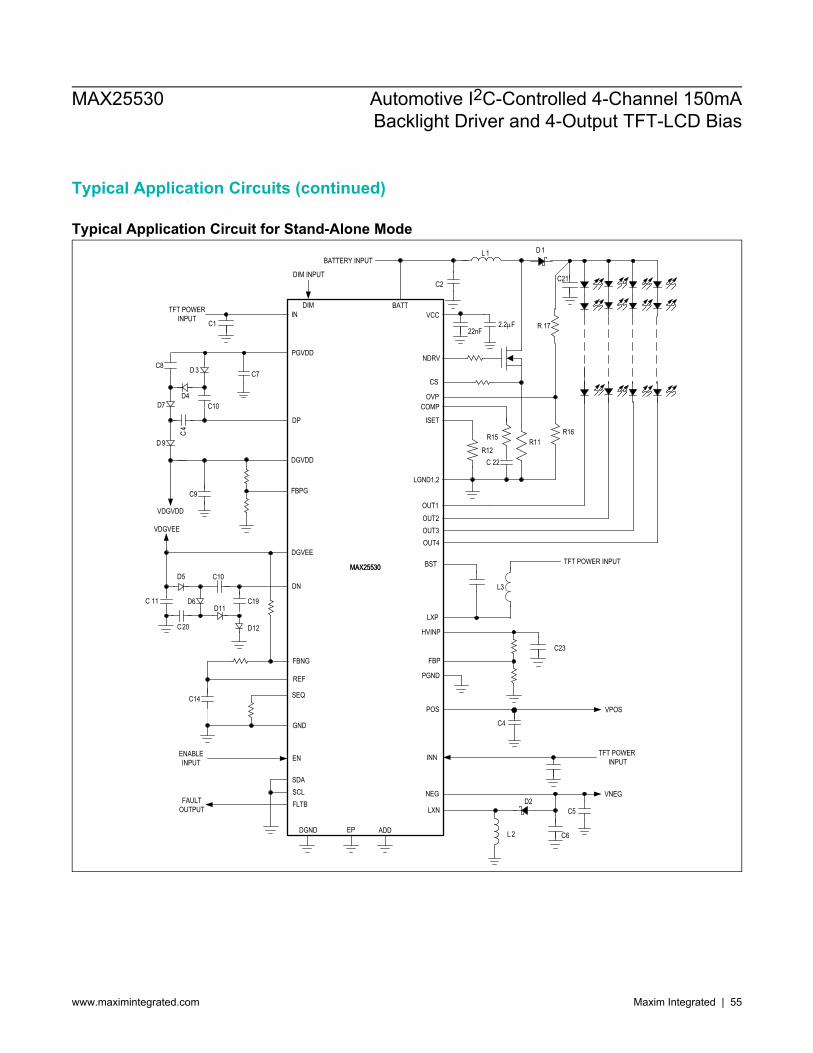
Typical Application Circuits (continued)
Typical Application Circuit for Stand-Alone Mode
MAX25530MAX25530
BATTVCC
NDRV
LGND1,2
COMP
CS
OVP
ISET
DIM
OUT1
LXP
FBP
INN
HVINP
POS
NEG
LXN
EP
EN
GND
SEQ
DN
DP
PGVDD
IN
DGVEE
DGVDD
FBPG
FBNG
REF
C1
BATTERY INPUT
C2C21
R15 R11R12
DIM INPUT
C23
C4
C5
C6L 2
D2
VPOS
VNEGFAULT
OUTPUT
TFT POWERINPUT
C7
C10
C9
VDGVDD
VDGVEE
C10
C19
C14
C 11
C20
D 3
D 9
D5
D11D6
D12
L3
R16
D4
C8
C4
D7
TFT POWER INPUT
FLTB
TFT POWER INPUT
R 17
C 22
L 1 D 1
OUT2OUT3OUT4
DGND ADD
PGND
SDASCL
BST
ENABLEINPUT
2.2mF22nF
MAX25530 Automotive I2C-Controlled 4-Channel 150mABacklight Driver and 4-Output TFT-LCD Bias
www.maximintegrated.com Maxim Integrated | 55
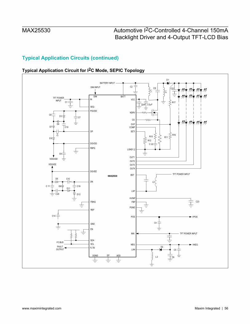
Typical Application Circuits (continued)
Typical Application Circuit for I2C Mode, SEPIC Topology
MAX25530MAX25530
BATTVCC
NDRV
LGND1,2
COMP
CS
OVP
SETI
DIM
OUT1
LXP
FBP
INN
HVINP
POS
NEG
LXN
EP
EN
GND
SEQ
DN
DP
PGVDD
IN
DGVEE
DGVDD
FBPG
FBNG
REF
C1
BATTERY INPUTC2
C21
R15 R11R12
DIM INPUT
C23
C4
C5
C6L 2
D2
VPOS
VNEGFAULT
OUTPUT
TFT POWERINPUT
C7
C10
C9
VDGVDD
VDGVEE
C10
C19
C14
C 11
C20
D 3
D 9
D5
D11D6
D12
L3
R16
D4
C8
C4
D7
TFT POWER INPUT
FLTB
TFT POWER INPUT
C 22
L1
D 1
OUT2OUT3OUT4
DGND ADD
PGND
SDASCL
I2C BUS
BST
L2
R17
CS
2.2mF22nF
MAX25530 Automotive I2C-Controlled 4-Channel 150mABacklight Driver and 4-Output TFT-LCD Bias
www.maximintegrated.com Maxim Integrated | 56
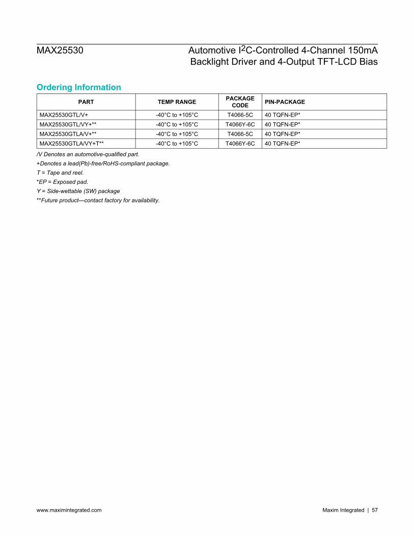
Ordering InformationPART TEMP RANGE PACKAGE
CODE PIN-PACKAGE
MAX25530GTL/V+ -40°C to +105°C T4066-5C 40 TQFN-EP*MAX25530GTL/VY+** -40°C to +105°C T4066Y-6C 40 TQFN-EP*MAX25530GTLA/V+** -40°C to +105°C T4066-5C 40 TQFN-EP*MAX25530GTLA/VY+T** -40°C to +105°C T4066Y-6C 40 TQFN-EP*
/V Denotes an automotive-qualified part.+Denotes a lead(Pb)-free/RoHS-compliant package.T = Tape and reel.*EP = Exposed pad.Y = Side-wettable (SW) package**Future product—contact factory for availability.
MAX25530 Automotive I2C-Controlled 4-Channel 150mABacklight Driver and 4-Output TFT-LCD Bias
www.maximintegrated.com Maxim Integrated | 57
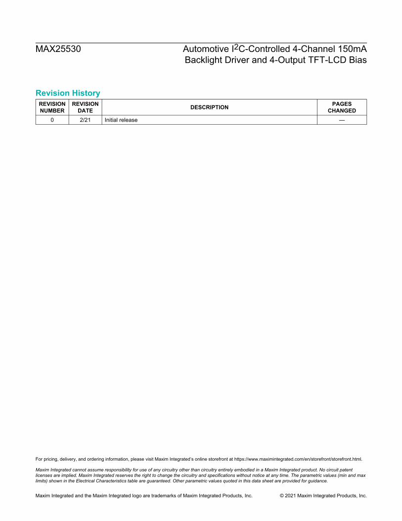
Revision HistoryREVISIONNUMBER
REVISIONDATE DESCRIPTION PAGES
CHANGED0 2/21 Initial release —
For pricing, delivery, and ordering information, please visit Maxim Integrated’s online storefront at https://www.maximintegrated.com/en/storefront/storefront.html.
Maxim Integrated cannot assume responsibility for use of any circuitry other than circuitry entirely embodied in a Maxim Integrated product. No circuit patentlicenses are implied. Maxim Integrated reserves the right to change the circuitry and specifications without notice at any time. The parametric values (min and maxlimits) shown in the Electrical Characteristics table are guaranteed. Other parametric values quoted in this data sheet are provided for guidance.
MAX25530 Automotive I2C-Controlled 4-Channel 150mABacklight Driver and 4-Output TFT-LCD Bias
Maxim Integrated and the Maxim Integrated logo are trademarks of Maxim Integrated Products, Inc. © 2021 Maxim Integrated Products, Inc.


![Automotive Computer Controlled Systems [h33t] [Malestrom]](https://img.pdfslide.us/doc/110x75/5456ec91b1af9fda448b4b33/automotive-computer-controlled-systems-h33t-malestrom-55844f1bd285e.jpg)