Embed Size (px)
Citation preview

CLEAR DISPLAY LTD.
LCD MODULE SPECIFICATION
Model Number : CD11020-01Product Type : COB, STN/Blue Sample Version: B
ADDRESS :#906 , HOSEO UNIV. VENTURE TOWER , GASAN-DONG , GEUMCHEON-GU SEOUL,KOREA TEL : 82-2-2068-9090 FAX : 82-2-2068-8970
Please return one copy with your official approval
CD LTD. SIGNATURES Department Name Signature
Prepared by (DE)
Checked by (QA)
Confirmed by (DE)
Approved by (DE Mgr.)
APPROVAL SIGNATURE Customer : __________________ Approved by : __________________ (Signature) Date : __________________

DOCUMENT REVISION HISTORY Version DATE DESCRIPTION CHANGED BY
A00 Nov-03-2011 First issue

1. GENERAL SPECIFICATIONS 1
2. ABSOLUTE MAXIMUM RATINGS 2
3. ELECTRICAL CHARACTERISTICS 4
4. ELECTRO-OPTICAL CHARACTERISTIC 4
5. TIMING CHARACTERISTICS 7
6. PIN CONNECTIONS 9
7. POWER SUPPLY 9
8. FUNCTIONAL DESCRIPTIONS 10
9. QUALITY ASSURANCE 16
10. PRECAUTIONS IN USE LCM 20
11 OUTLINE DRAWING 21
12. PACKAGE INFORMATION 22 13. LABEL MARKING 23

Confidential Document
Page: 1
1. GENERAL SPECIFICATION Display Format : 20characters (W) × 4lines (H)
Character Size : 2.95 (W) × 4.75 (H) mm
View Area : 76.0 (W) × 25.2 (H) mm
General Dimensions : 98.0 (W) × 60.0 (H) × 15.0 (T) mm Max.
Weight : TDB g max.
LCD Type : V
STN/Blue
STN Y-G
FSTN
Polarizer mode :
Reflective
Transflective
V Transmissive V
Negative
V View Angle :
6 O’clock
12 O’clock
Others
V Backlight :
LED
EL
CCFL
V
Backlight Color :
Yellow green
Amber
Blue Green
White
Others
Controller / Driver : SPLC780D1 & SPLC063B
Normal V Wide Temperature Operating 0 to 50°C Operating -20 to 70°C
Temperature Range :
Storage -20 to 70°C Storage -30 to 80°C

Confidential Document
Page: 2
2. ABSOLUTE MAXIMUM RATINGS
2.1 ELECTRICAL ABSOLUTE MAXIMUM RATINGS
VSS= 0V, Ta = 25°C Item Symbol Min. Max. Unit
Supply Voltage (Logic) VDD-VSS 0 7 V
Supply Voltage (LCD Driver) VDD-V0 -0.3 VDD+0.3V V
Input Voltage VI VSS VDD V
Operating Temperature TOP -20 70 °C
Storage Temperature TSTG -30 80 °C
2.2 ENVIRONMENTAL ABSOLUTE MAXIMUM RATINGS
Operating Storage Item
(Min.) Max.) (Min.) (Max.) Comment
Ambient Temp -20 70 -30 80 Note (1) Note(2) Without Condensation Vibration -- 4.9M/S2 -- 19.6M/S2 XYZ Direction
Shock -- 29.4M/S2 -- 490M/S2 XYZ Direction
Note(1) Ta = 0°C : 50Hr Max. Note(2) Ta ≤ 40°C : 90% RH Max. Ta ≥ 40°C : Absolute humidity must be lower than the humidity of 90% RH at 40°C.

Page: 3
2.3 Electronic Static Discharge maximum rating
ESD test method : IEC1000-4-2 Item Description
Testing environment Ambient temperature :15°C to 35 °C Humidity: 30% to 60 % LCM ( E.U.T ) : Power up
Testing equipment Manufacture: NoiseKen, Model No. ESD-100L Testing condition See drawing 1 Direct discharge 0 to ± 6 KV Discharge point, see drawing 2 Indirect discharge 0 to ± 12KV Discharge point, see drawing 1 Pass condition No malfunction of unit. Temporary malfunction of unit which
can be recovered by system reset Fail condition Non. Recoverable malfunction of LCM or system
(1)
(2)
D IR E C T D ISC H A R G E
H C P IN D IR EC T D ISC H A R G E
G R O U N D LE V E L
V C P IN D IR EC T D ISC H A R G E
H C P
ISO LA T O R
E SD PO W ER SU PPLY
W O O D E N T A B LE (T A LL 0.8m )
470k
F IG 1 ESD T ESTIN G EQ U IPM E N T
AB
DC
DIRECT CONTACT DISCHARGECONTACT POINT : A.B.C.D

Confidential Document
Page: 4
3. ELECTRICAL CHARACTERISTICS
Item Symbol Condition Min. Typ. Max. Unit
Supply Voltage (Logic) VDD-VSS 4.8 5.0 5.2 V
0°C 4.3 4.5 4.7 25°C 4.1 4.3 4.5
Supply Voltage (LCD) VDD-V0
50°C 3.9 4.1 4.3 V
VIH -- 0.7∗VDD -- VDD Input Voltage
VIL VSS -- 0.3∗VDD V
Logic Supply Current IDD VDD-VSS=5V -- 2.0 -- mA
4. ELECTRO-OPTICAL CHARACTERISTICS
ITEM Symbol Condition Min. Typ. Max. Unit Ref.
0°C 1100 1800 Rise Time Tr
25°C --
120 250 ms
0°C 210 340 Fall Time Tf 25°C
-- 100 200
ms Note (1)
Contrast CR 25°C 3 Note (3)
-- 80 -- View Angle θ1~θ2 ∅1, ∅2
25°C & CR≥3 -- 60 -- Note (2)
Frame Frequency Ff 25°C -- 64 -- Hz
Note (1) & (2) : See next page Note (3) : Contrast ration is defined under the following condition: CR= Brightness of non-selected condition Brightness of selected condition ( a ). Temperature ---------- 25°C ( b ). Frame frequency ---- 64Hz ( c ). Viewing angle -------- θ= 0°, ∅ = 0° ( d ). Operating voltage --- 5.0V

Page: 5
Note (1) Response time is measured as the shortest period of time possible between the change in state of an LCD segment as demonstrated below: +Vop 1/f F 0 -Vop 90% 100% 10% tr tf Condition: ( a ) . Temperature ---------------25°C ( b ) . Frame frequency --------- 64Hz ( c ) . View Angle ----------------- θ = 0°, ∅=0° ( d ) . Operating voltage -------- 5.0V Note (2) Definition of View Angle Top – Bottom direction Right -- Left direction Top ∅2 ∅1 θ1 θ2 Bottom Left Right

Page: 6
LED ELECTRO-OPTICAL CHARACTERISTIC Ta = 25°C
Item Symbol Condition Min. Typ. Max. Unit
Forward Voltage VF IF = 60mA White 4.8 5.0 5.2 V
Luminous Intensity IV IF = 60mA White 200 -- -- mcd
Reverse Current IR VR = 5V White -- -- 0.04 mA
Note : Measured at the bared LED backlight unit. LED MAXIMUM OPERATING RANGE
Item Symbol Yellow Green Unit Power Dissipation PAD 312 mW Forward Current IAF 100 mA Reverse Voltage VR 5 V
LED ARRAY BLOCK DIAGRAM
CoordinatesChromaticity X If= 60 mA - 0.29 - Y
White - 0.29 -
LED POWER SOURCE
LED
Option Power source Jumper settingA 15A/16K R8, R9,R11, R14B 15K/16A R8,R9,R12,R15
C VDD/VSS R8, R9, R10, R13
GND FRM GND R16
Note: R11=R14= 0 ohm, R10=R12=R13=R15= Open R8= 40 ohm, R9= 20 ohmR16= 0 ohm or 1M ohm, it depends on ESD status

Page: 7
5. TIMING CHARACTERISTICS
5.1 Write mode (Writing data from MPU to SPLC780D1) Limit Characteristics Symbol
Min. Typ. Max. Unit Test Condition
E Cycle Time tC 1000 - - ns Pin E
E Pulse Width tPW 450 - - ns Pin E
E Rise/Fall Time tR, tF - - 25 ns Pin E
Address Setup Time tSP1 60 - - ns Pins: RS, R/W, E
Address Hold Time tHD1 20 - - ns Pins: RS, R/W, E
Data Setup Time tSP2 195 - - ns Pins: DB0 - DB7
Data Hold Time tHD2 10 - - ns Pins: DB0 - DB7
Write mode timing diagram (Writing Data from MPU to SPLC780D1)
RS
R / W
E
DB7 - 0
VIH1
VIL1
VIH1
VIL1
VIL1
tSP1
tC
Valid DataVIH1
VIL1
VIH1
VIL1
VIH1
VIL1
VIH1
VIL1
VIL1
tHD1
tHD1tFtPW
tHD2tSP2
tR
VIL1
Page: 8
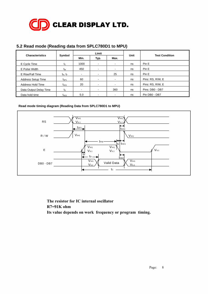
5.2 Read mode (Reading data from SPLC780D1 to MPU) Limit
Characteristics Symbol Min. Typ. Max.
Unit Test Condition
E Cycle Time tC 1000 - - ns Pin E
E Pulse Width tW 450 - - ns Pin E
E Rise/Fall Time tR, tF - - 25 ns Pin E
Address Setup Time tSP1 60 - - ns Pins: RS, R/W, E
Address Hold Time tHD1 20 - - ns Pins: RS, R/W, E
Data Output Delay Time tD - - 360 ns Pins: DB0 - DB7
Data hold time tHD2 5.0 - - ns Pin DB0 - DB7
Read mode timing diagram (Reading Data from SPLC780D1 to MPU)
RS
R / W
E
DB0 - DB7
VIH1
VIL1
VIH1
VIL1
tSP1
tC
Valid DataVIH1
VIL1
VIH1
VIL1
VIH1
VIL1
VIH1
VIL1
tHD1
tHD1tFtPW
tHD2
tR
VIL1
VIH1 VIH1
tD
The resistor for IC internal oscillatorR7=91K ohm Its value depends on work frequency or program timing.

Page: 9
6. PIN CONNECTIONS
No. Symbol Function 1 VSS Ground, 0V 2 VDD Logic power supply, +5V 3 V0 Voltage for LCD drive 4 RS Data / Instruction register select 5 R/W Read / Write 6 E Enable signal, start data read/write 7 DB0 8 DB1 9 DB2 10 DB3 11 DB4 12 DB5 13 DB6 14 DB7
Data Bus Line
15 LED A LED Anode, power supply +5V 16 LED K LED Cathode, ground 0V
7. POWER SUPPLY VDD +5V VSS VR V0 +5V LED A LED K VR = 10K

Page: 10
8.1 BLOCK DIAGRAM
8. FUNCTIONAL DESCRIPTIONS
LCDCOM 1-16
SEG 121-200
CONTROLLERVSSVDDVEE
RS
R/W
D0 D7
E
20 character×4 line
SEGMENT
SEG 1-40
SEG 41-1204
SEGMENTSEGMENT DRIVER
4 DRIVER
SPLC780D
R1=R2=R4=R5=1.0K ohm R3=R6=0 ohm, R17 N.C.
8.2 BIAS CIRCUIT DIAGRAM
Page: 11
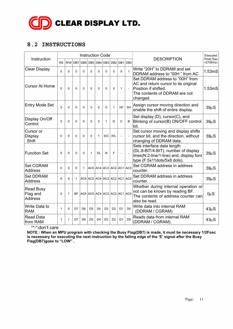
8.2 INSTRUCTIONS
Instruction Code Instruction
RS R/W DB7 DB6 DB5 DB4 DB3 DB2 DB1 DB0 DESCRIPTION
Executed Time( fosc =270KHz)
Clear Display 0 0 0 0 0 0 0 0 0 1 Write “20H” to DDRAM and set
DDRAM address to “00H ” from AC 1.53mS
Cursor At Home 0 0 0 0 0 0 0 0 1 -
Set DDRAM address to “00H” from AC and return cursor to its original Position if shifted. The contents of DDRAM are not changed.
1.53mS
Entry Mode Set 0 0 0 0 0 0 0 1 I/D SH Assign cursor moving direction and
enable the shift of entire display. 39µS
Display On/Off Control 0 0 0 0 0 0 1 D C B
Set display (D), cursor(C), and Blinking of cursor(B) ON/OFF control bit.
39µS
Cursor or Display Shift
0 0 0 0 0 1 S/C R/L - - Set cursor moving and display shifts cursor bit, and the direction, without changing of DDRAM data.
39µS
Function Set 0 0 0 0 1 DL N F - -
Sets interface data length (DL:8-BIT/4-BIT), number of display lines(N:2-line/1-line) and, display font type (F:5x11dots/5x8 dots).
39µS
Set CGRAM Address 0 0 0 1 AC5 AC4 AC3 AC2 AC1 AC0 Set CGRAM address in address
counter. 39µS
Set DDRAM Address 0 0 1 AC6 AC5 AC4 AC3 AC2 AC1 AC0 Set DDRAM address in address
counter. 39µS
Read Busy Flag and Address
0 1 BF AC6 AC5 AC4 AC3 AC2 AC1 AC0
Whether during internal operation or not can be known by reading BF. The contents of address counter can also be read.
0µS
Write Data to RAM 1 0 D7 D6 D5 D4 D3 D2 D1 D0 Write data into internal RAM
(DDRAM / CGRAM) 43µS
Read Data from RAM 1 1 D7 D6 D5 D4 D3 D2 D1 D0 Reads data from internal RAM
(DDRAM / CGRAM). 43µS
*"-":don’t care NOTE : When an MPU program with checking the Busy Flag(DB7) is made, it must be necessary 1/2Fosc is necessary for executing the next instruction by the falling edge of the ‘E’ signal after the Busy Flag(DB7)goes to “LOW” .

Page: 12
8.3 Interfacing to the MPU
The IC can send data in either two 4-bit operations, thus allowing interfacing with 4- or 8-bit MPUs.
• For 4-bit interface data, only four bus lines (DB4 to DB7) are used for
transfer. Bus lines DB0 to DB3 are disabled. The data transfer between the IC and the MPU is completed after the 4-bit data has been transferred twice. As for the order of data transfer, the four high order bits (for 8-bit operation,DB4 to DB7) are transferred before the four low order bits (for 8-bit operation, DB0 to DB3). The busy flag must be checked (one instruction) after the 4-bit data has been transferred twice. Two more 4-bit operations then transfer the busy flag and address counter data.
RS R/W E
DB7 IR7 IR3 BF AC3 DR7 DR3
DB6 IR6 IR2 AC6 AC2 DR6 DR2
DB5 IR5 IR1 AC5 AC1 DR5 DR1
DB4 IR4 IR0 AC4 AC0 DR4 DR0
Instruction register (IR)
write Busy flag (BF) and Address counter (AC) read
Data register (DR) read
4-Bit Transfer Example

Page: 13
8.4 1-Line Display Display
position 1 2 3 4 5 6 7 8 9 10 11 12 13 14 15 16
DDRAM 00 01 02 03 04 05 06 07 40 41 42 43 44 45 46 47
Address (hexadecimal) 16×1–Line
2-Line Display Display
position 1 2 3 4 5 ⋅ ⋅ ⋅8⋅ ⋅ ⋅16⋅ ⋅ ⋅20⋅ ⋅ ⋅24⋅ ⋅ ⋅ 39 40
DDRAM 00 01 02 03 04 ⋅ ⋅ ⋅ ⋅ ⋅ ⋅ ⋅ ⋅ ⋅ ⋅ ⋅ ⋅ ⋅ ⋅ ⋅ ⋅ ⋅ ⋅ 26 27
Address (hexadecimal) 40 41 42 43 44 ⋅ ⋅ ⋅ ⋅ ⋅ ⋅ ⋅ ⋅ ⋅ ⋅ ⋅ ⋅ ⋅ ⋅ ⋅ ⋅ ⋅ ⋅ 66 67
8×2–Line 16×2–Line 20×2–Line 24×2–Line
4-Line Display Display
position 1 2 3 ⋅ ⋅ ⋅ ⋅ ⋅ ⋅ ⋅ ⋅ ⋅ ⋅ ⋅ ⋅ ⋅ ⋅ ⋅ ⋅ ⋅ ⋅ ⋅ ⋅ ⋅ ⋅ ⋅ ⋅ ⋅ ⋅ ⋅ ⋅ 15 16
DDRAM 00 01 02 ⋅ ⋅ ⋅ ⋅ ⋅ ⋅ ⋅ ⋅ ⋅ ⋅ ⋅ ⋅ ⋅ ⋅ ⋅ ⋅ ⋅ ⋅ ⋅ ⋅ ⋅ ⋅ ⋅ ⋅ ⋅ ⋅ ⋅ ⋅ 0E 0F
Address (hexadecimal) 40 41 42 4E 4F
14 15 16 1E 1F
54 55 56 5E 5F
16×4 Line
Display
position 1 2 3 ⋅ ⋅ ⋅ ⋅ ⋅ ⋅ ⋅ ⋅ ⋅ ⋅ ⋅ ⋅ ⋅ ⋅ ⋅ ⋅ ⋅ ⋅ ⋅ ⋅ ⋅ ⋅ ⋅ ⋅ ⋅ ⋅ ⋅ ⋅ 19 20
DDRAM 00 01 02 ⋅ ⋅ ⋅ ⋅ ⋅ ⋅ ⋅ ⋅ ⋅ ⋅ ⋅ ⋅ ⋅ ⋅ ⋅ ⋅ ⋅ ⋅ ⋅ ⋅ ⋅ ⋅ ⋅ ⋅ ⋅ ⋅ ⋅ ⋅ 12 13
Address (hexadecimal) 40 41 42 52 53
14 15 16 26 27
54 55 56 66 67
20×4 Line

Page: 14
8.5 CGRAM
Relationship between CGRAM Addresses, Character Codes (DDRAM) and Patterns (CGRAM Data) For 5×8 dot character patterns
Character Codes (DDRAM data) CGRAM Address Character Patterns
(CGRAM data)
7 6 5 4 3 2 1 0 5 4 3 2 1 0 7 6 5 4 3 2 1 0
High Low
High Low
High Low
0 0 0 ∗ ∗ ∗ 1 1 1 1 0 0 0 1 1 0 0 0 1 0 1 0 1 0 0 0 1 0 1 1 1 1 1 1 0 1 0 0 1 0 1 0 0 1 0 1 1 0 0 1 0 1 1 0
1 0 0 0 1
Character Pattern (1)
0 0 0 0 ∗ 0 0 0 0 0 0
1 1 1
∗ ∗ ∗ 0 0 0 0 0 } Cursor position 0 0 0 ∗ ∗ ∗ 1 0 0 0 1 0 0 1 0 1 0 1 0 0 1 0 1 1 1 1 1 0 1 1 0 0 1 0 0 1 0 0 1 1 1 1 1 1 0 1 0 0 1 0 0 1 1 0
0 0 1 0 0
Character Pattern (2) 0 0 0 0 ∗ 0 0 1 0 0 1
1 1 1
∗ ∗ ∗ 0 0 0 0 0 } Cursor position 0 0 0 ∗ ∗ ∗ 0 0 1
1 1 1 1 0 0 1 0 1 1 1 0
0 0 0 0 ∗ 1 1 1
1 1 1
∗ ∗ ∗
Notes : 1. Character code bits 0 to 2 correspond to CGRAM address bits 3 to 5 (3 bits: 8 types). 2. CGRAM address bits 0 to 2 designate the character pattern line position. The 8t h line
is the cursor position and its display is formed by a logical OR with the cursor. Maintain the 8t h line data, corresponding to the cursor display position, at 0 as the cursor display. If the 8t h line data is 1, 1 bits will light up the 8t h line regardless of the cursor presence.
3. Character pattern row positions correspond to CGRAM data bits 0 to 4 (bit 4 being at the left).
4. As shown Table 5, CGRAM character patterns are selected when character code bits 4 to 7 are all 0. However, since character code bit 3 has no effect, the R display example above can be selected by either character code 00H or 08H.
5. 1 for CGRAM data corresponds to display selection and 0 to non-selection. ∗ Indicates no effect.

Page: 15
8.6 Correspondence between Character Codes and Character Patterns (ROM Code:A00)

Page: 16
9. QUALITY ASSURANCE
9.1 Test Condition
9.1.1 Temperature and Humidity(Ambient Temperature) Temperature : 20 ± 5°C Humidity : 65 ± 5%
9.1.2 Operation
Unless specified otherwise, test will be conducted under function state.
9.1.3 Container Unless specified otherwise, vibration test will be conducted to the product itself without putting it in a container.
9.1.4 Test Frequency
In case of related to deterioration such as shock test. It will be conducted only once.
9.1.5 Test Method No. Parameter Conditions Regulations 1 High Temperature Operating 70 ± 2 °C Note 3 2 Low Temperature Operating - 2 0 ± 2 °C Note 3 3 High Temperature Storage 80 ± 2 °C Note 3 4 Low Temperature Storage - 30 ± 2 °C Note 3
5
Vibration Test (Non-operation state)
Total fixed amplitude : 1.5mm Vibration Frequency : 10 ~ 55Hz One cycle 60 seconds to 3 directions of X.Y.Z. for each 15 minutes
Note 3
6 Damp Proof Test (Non-operation state)
40°C ± 2°C, 90~95%RH, 96h Note 1,2
7 Shock Test (Non-operation state)
To be measured after dropping from 60cm high once concrete surface in packing state
Note 3
Note 1: Returned under normal temperature and humidity for 4 hrs. Note 2: No dew condensation to be observed. Note 3: No change on display and in operation under the test condition

Page: 17
9.2 Inspection condition 9.2.1 Inspection conditions
The LCD shall be inspected under 40W white fluorescent light.
45°
9.2.2 Definition of applicable Zones
B LCD A BEZEL PCB A : Display Area B : Non-Display Area
Page: 18
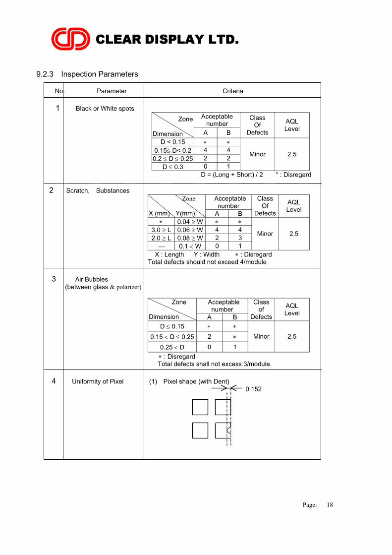
9.2.3 Inspection Parameters
No. Parameter Criteria
1 Black or White spots Acceptable
number Zone Dimension A B
Class Of
Defects
AQL Level
D < 0.15 ∗ ∗ 0.15≤ D< 0.2 4 4 0.2 ≤ D ≤ 0.25 2 2
D ≤ 0.3 0 1
Minor 2.5
D = (Long + Short) / 2 * : Disregard
2 Scratch, Substances Acceptable
number X (mm)
Zone Y(mm) A B
Class Of
Defects
AQL Level
∗ 0.04 ≥ W ∗ ∗ 3.0 ≥ L 0.06 ≥ W 4 4 2.0 ≥ L 0.08 ≥ W 2 3 0.1 < W 0 1
Minor 2.5
X : Length Y : Width ∗ : Disregard Total defects should not exceed 4/module
3 Air Bubbles (between glass & polarizer)
Acceptable number
Zone Dimension A B
Class of
Defects
AQL Level
D ≤ 0.15 ∗ ∗ 0.15 < D ≤ 0.25 2 ∗
0.25 < D 0 1 Minor 2.5
∗ : Disregard Total defects shall not excess 3/module.
4 Uniformity of Pixel (1) Pixel shape (with Dent) 0.152

Page: 19
4 Uniformity of Pixel
(2) Pixel shape ( with Projection) Should not be connected to
next pixel 0.152 (3) Pin hole X Y ( X + Y )/2 ≤ 0.02mm (Less than 0.1 mm is no counted) (4) Deformation
X ( X + Y ) / 2 ≤ 0.3mm Y Total acceptable number : 1/pixel, 5/cell
Definition
Major AQL 0.65% It is a defect that is likely to result in failure or to reduce materially the usability of the product for the intended function.
AQL 1.00% It is a defect that is likely to assembly size and not result in functioning problem.
Class of defects
Minor AQL 2.5% It is a defect that will not result in functioning problem with deviation classified.

Page: 20
10. PRECAUTION FOR USING LCM
1. LIQUID CRYSTAL DISPLAY (LCD) LCD is made up of glass, organic sealant, organic fluid, and polymer based polarizers. The following precautions should be taken when handing, (1). Keep the temperature within range of use and storage. Excessive temperature and humidity could cause polarization degredation, polarizer peel off or bubble. (2). Do not contact the exposed polarizers with anything harder than an HB pencil lead. To clean dust off the display surface, wipe gently with cotton, chamois or other soft material soaked in petroleum benzin. (3). Wipe off saliva or water drops immediately. Contact with water over a long period of time may cause polarizer deformation or color fading, while an active LCD with water condensation on its surface will cause corrosion of ITO electrodes. (4). Glass can be easily chipped or cracked from rough handling, especially at corners and edges. (5). Do not drive LCD with DC voltage. 2. Liquid Crystal Display Modules 2.1 Mechanical Considerations LCM are assembled and adjusted with a high degree of precision. Avoid excessive shocks and do not make any alterations or modifications. The following should be noted. (1). Do not tamper in any way with the tabs on the metal frame. (2). Do not modify the PCB by drilling extra holes, changing its outline, moving its components or modifying its pattern. (3). Do not touch the elastomer connector, especially insert an backlight panel (for example, EL). (4). When mounting a LCM make sure that the PCB is not under any stress such as bending or twisting . Elastomer contacts are very delicate and missing pixels could result from slight dislocation of any of the elements. (5). Avoid pressing on the metal bezel, otherwise the elastomer connector could be deformed and lose contact, resulting in missing pixels. 2.2. Static Electricity LCM contains CMOS LSI’s and the same precaution for such devices should apply, namely (1). The operator should be grounded whenever he/she comes into contact with the module. Never touch any of the conductive parts such as the LSI pads, the copper leads on the PCB and the interface terminals with any parts of the human body. (2). The modules should be kept in antistatic bags or other containers resistant to static for storage. (3). Only properly grounded soldering irons should be used. (4). If an electric screwdriver is used, it should be well grounded and shielded from commutator sparks.
(5) The normal static prevention measures should be observed for work clothes and working benches; for the latter conductive (rubber) mat is recommended. (6). Since dry air is inductive to statics, a relative humidity of 50-60% is recommended. 2.3 Soldering (1). Solder only to the I/O terminals. (2). Use only soldering irons with proper grounding and no leakage. (3). Soldering temperature : 280°C ± 10°C (4). Soldering time: 3 to 4 sec. (5). Use eutectic solder with resin flux fill. (6). If flux is used, the LCD surface should be covered to avoid flux spatters. Flux residue should be removed after wards. 2.4 Operation (1). The viewing angle can be adjusted by varying the LCD driving voltage V0. (2). Driving voltage should be kept within specified range; excess voltage shortens display life. (3). Response time increases with decrease in temperature. (4). Display may turn black or dark blue at temperatures above its operational range; this is (however not pressing on the viewing area) may cause the segments to appear “fractured”. (5). Mechanical disturbance during operation (such as pressing on the viewing area) may cause the segments to appear “fractured”. 2.5 Storage If any fluid leaks out of a damaged glass cell, wash off any human part that comes into contact with soap and water. Never swallow the fluid. The toxicity is extremely low but caution should be exercised at all the time. 2.6 Limited Warranty Unless otherwise agreed between CLEAR and customer, CLEAR will replace or repair any of its LCD and LCM which is found to be defective electrically and visually when inspected in accordance with CLEAR acceptance standards, for a period on one year from date of shipment. Confirmation of such date shall be based on freight documents. The warranty liability of CLEAR is limited to repair and/or replacement on the terms set forth above. CLEAR will not responsible for any subsequent or consequential events.

page: 21
11. DIMENSIONAL OUTLINE

Page 22
12. Package method
415x365x430mm
Page: 23
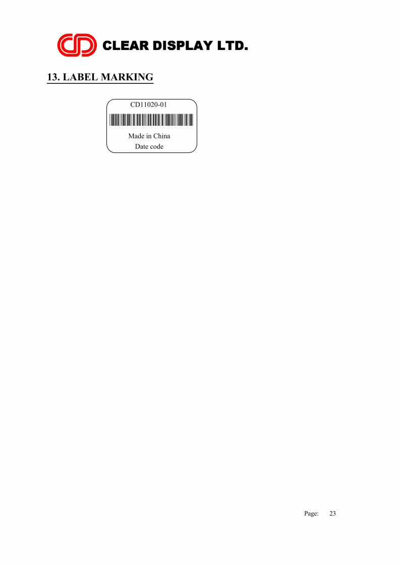
13. LABEL MARKING
CD11020-01
Made in China Date code