Embed Size (px)
DESCRIPTION
Classical Control for Quantum Computers. Mark Whitney, Nemanja Isailovic, Yatish Patel, John Kubiatowicz U.C. Berkeley. Quantum Computing is Hard. Qubit decoherence Physical isolation from environment Error correction correcting error correction! Decoherence-free subspaces. - PowerPoint PPT Presentation
Citation preview
Classical Control for Quantum Computers
Mark Whitney, Nemanja Isailovic, Yatish Patel, John Kubiatowicz
U.C. Berkeley
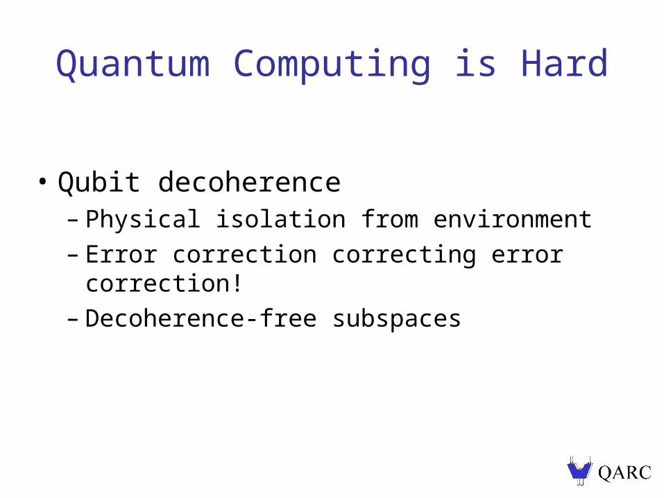
Quantum Computing is Hard
• Qubit decoherence– Physical isolation from environment– Error correction correcting error correction!– Decoherence-free subspaces

Quantum Computing is Harder!
• Complex physical interactions = complex pulse sequences
• Nanoscale geometries– Atomic interactions on the order of 10nm
• Cold operating temperatures– 1 Kelvin reduces thermal noise
• These issues make control circuitry difficult!
• Must account for in QC design
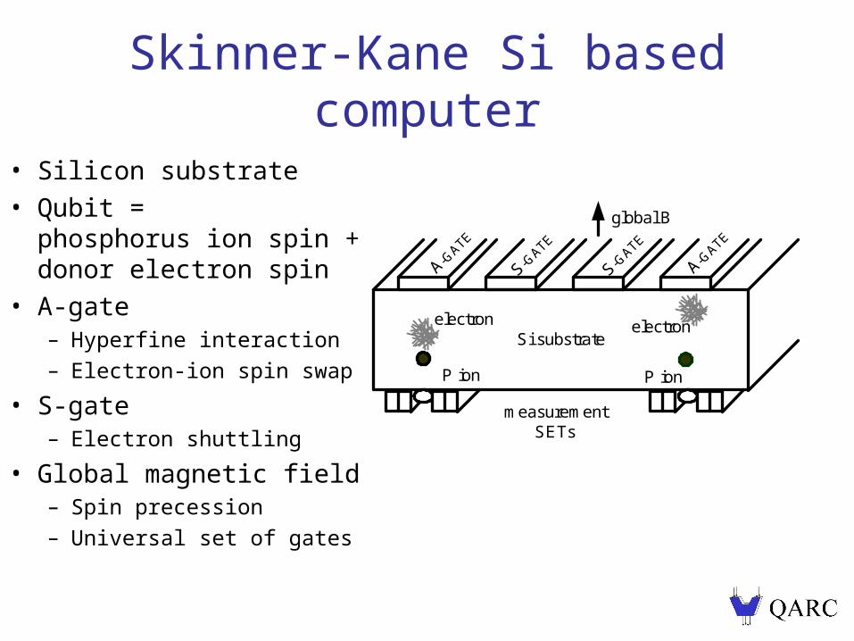
Skinner-Kane Si based computer
• Silicon substrate• Qubit =
phosphorus ion spin + donor electron spin
• A-gate– Hyperfine interaction– Electron-ion spin swap
• S-gate– Electron shuttling
• Global magnetic field– Spin precession– Universal set of gates
Si substrate
A-GATE
S-GATE
S-GATE
P ion P ion
electron electron
global B
measurementSETs
A-GATE

Quantum wires
• Ions are stationary– Qubits are moved by swapping
• Alternating swap gives us “wires”– Some qubits move right, some left
• Quantum wires seem more complicated than classical…
S A S S A S S S S S SA A. . . . . .1 2 3 42 1 4 30 4 1 504 5 1

S A S S A S
Swap cell
• A lot of steps for two qubits!
e1- e2
-e2-e1
- e2-e2
-
e2-
Electron-ion spin swap
e2- e2
- e2-e1
- e2-e1
- e2-e1
- e1-
e1-
Electron-ion spin swap
e1-e1
-e1- e2
-e1-
P ion 1 P ion 2
S A S S A S S S S S SA A. . . . . .
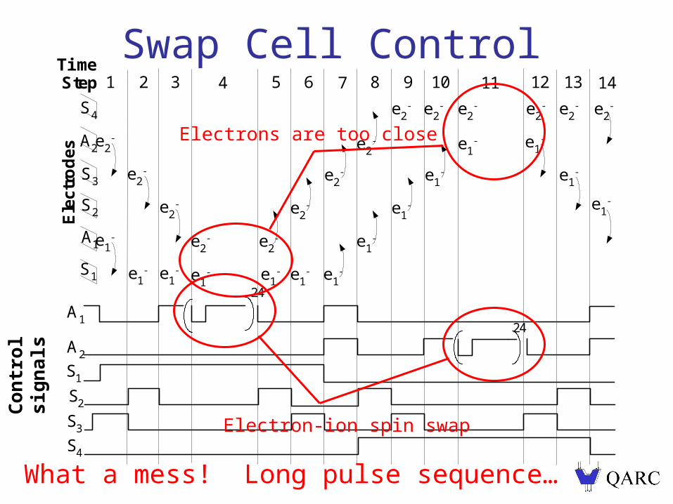
Swap Cell Control
• What a mess! Long pulse sequence…
e1-
e2-
S1
A1
S2
S3
A2
S4
e1-e1
-
e2-
e2-
e2-
e1-
e1-
e2-
e1-
e2-
e1-
e2-
e1-
e2-
e1-
e2-
e1-
e2-
e1-
e2-
e1-
e2-
e1-
e2- e2
-
e1-
S1
S2
S3
A1
S4
A2
24
24
Step 1 2 3 4 5 6 7 8 9 10E
lect
rod
es11 12 13 14
Electron-ion spin swap
Time
Co
ntr
ol
sig
na
ls
Electrons are too close
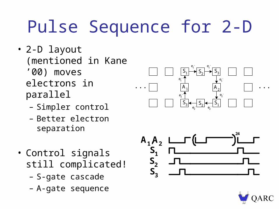
Pulse Sequence for 2-D• 2-D layout (mentioned
in Kane ’00) moves electrons in parallel– Simpler control– Better electron
separation
• Control signals still complicated!– S-gate cascade– A-gate sequence
S1S2S3
A1,A2
24
A1 A2
S1 S3
S3 S2S1
S2
e1-
e1-
e1-
e1-
e2-e2
-
e2- e2
-
. . .. . .
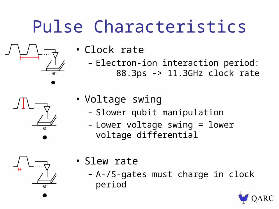
Pulse Characteristics• Clock rate
– Electron-ion interaction period: 88.3ps -> 11.3GHz clock rate
• Voltage swing– Slower qubit manipulation– Lower voltage swing = lower voltage
differential
• Slew rate– A-/S-gates must charge in clock period
. . .
e-
. . .. . .
e-
. . .. . .
e-
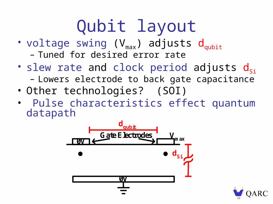
Qubit layout• voltage swing (Vmax) adjusts dqubit
– Tuned for desired error rate• slew rate and clock period adjusts dSi
– Lowers electrode to back gate capacitance• Other technologies? (SOI)• Pulse characteristics effect quantum datapath
0V
0V
dSi
Gate Electrodes Vmax
dqubit

Single-electron transistors (SETs)
• CMOS does not work at 1K operating temperature• SETs work well at low temperatures• Electrons move 1-by-1 through tunnel junction onto
quantum dot and out other side• Low drive current (~5nA) and voltage swing (~40mV)
– Affects our error and slew rates
Tunnel Junction
VDD
VDD
Control Input
Island
CLOAD
Y. Takahashi et. al.

Swap control circuit
• S-/A-gate pulse sequences complex
• What would a circuit schematic look like?
S1S2S3
A1,A2
24
A1 A2
S1 S3
S3 S2S1
S2
e1-
e1-
e1-
e1-
e2-e2
-
e2- e2
-
. . .. . .
5-bit counter
01234
Reset
Enable
8-bit counter
Reset
1
2
3
4
5
6
7
0
D D D D D D D
D D D D D D D
S1a S1b
S1c S1d
S2a
S2b
S3a S3b
S3c S3d
S4a
S4b
TD
S1a
S1b
S1c
S1d
S1 on
S3a
S3b
S3c
S3d
S3 on
S2a
S2bS2 on
S4a
S4bS4 on
Aa
S1 on
S2 on
S3 on
S4 on
Aa
Aon
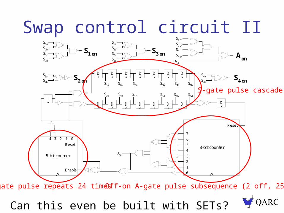
Swap control circuit II
Off-on A-gate pulse subsequence (2 off, 254 on)A-gate pulse repeats 24 times
• Can this even be built with SETs?
S-gate pulse cascade

Large!
• Control circuit area, ~10um2
– Aggressive process, 30nm feature size
– Minimal design
• Swap cell area, ~0.068um2
• Will not fit!
S1S2S3
A1,A2
24
A1 A2
S1 S3
S3 S2S1
S2
e1-
e1-
e1-
e1-
e2-e2
-
e2- e2
-
. . .. . .

In SIMD we trust?• Large control circuit/small swap cell ratio = SIMD• Like clock distribution network• Clock skew at 11.3GHz?• Error correction?
SwapControl
A
A
S1
S3
S3
S2
S1
S2
A S3
S2
S1
S2
A S3
S2
S1
S2
A S3
S2
S1
S2
A
A
S1
S3
S3
S2
S1
S2
A S3
S2
S1
S2
A S3
S2
S1
S2
A S3
S2
S1
S2
.
.
.
.
.
.
.
.
.
.
.
.

Why on-chip?• Why not run many wires
in from outside?• Error correction
complicates– Requires conditional
swapping
1000 qubits
* 336 swaps/lvl 1 ECC
* 4 signals/qubit in swap
= 1344000 wires!
• ECC could mean trouble for SIMD in general
1,000,000 wire bus!

Conclusions
• Pulse sequences for quantum gates are complex!
• All quantum computing technologies require complex pulse sequences
• Must keep control circuit in mind for large-scale integration