Embed Size (px)
Citation preview
Applied Physics Research; Vol. 7, No. 2; 2015ISSN 1916-9639 E-ISSN 1916-9647
Published by Canadian Center of Science and Education
Circular and Periodic Circular Profiles in a Rectangular CrossSection Along the Straight Waveguide
Z. Menachem1 & S. Tapuchi1
1 Department of Electrical and Electronics Engineering, Sami Shamoon College of Engineering, Israel
Correspondence: Z. Menachem, Department of Electrical and Electronics Engineering, Sami Shamoon College ofEngineering, Israel. E-mail: [email protected]
Received: February 15, 2015 Accepted: March 1, 2015 Online Published: March 20, 2015
doi:10.5539/apr.v7n2p121 URL: http://dx.doi.org/10.5539/apr.v7n2p121
Abstract
The first objective of this paper is to present a technique and a particular application to calculate the dielectricprofile, the elements of the matrix, and its derivatives of the dielectric profile in the cases of circular and periodiccircular profiles in the cross section of the rectangular straight waveguide. The second objective is to investigatethe influence of the circular and periodic circular profiles on the output fields. The proposed technique relates tothe method that is based on the Laplace and Fourier transforms, the inverse Laplace and Fourier transforms. Thismodel is useful to predict the structure of the output fields for circular and periodic circular profiles in a rectangularmetallic waveguide. The application is useful for straight waveguides in the microwave and the millimeter-waveregimes.
Keywords: wave propagation, dielectric profiles, straight metallic waveguide, rectangular cross section, dielectricwaveguide
1. Introduction
The methods of straight waveguides have been proposed in the literature. A method of selective suppressionof electromagnetic modes in rectangular waveguides by loading distributed losses in some special position ofwaveguide inner wall has been presented (Jiao, 2011). In this paper, the unwanted modes can be attenuated muchlarger relative to the operating mode and this proposed method can be used to improve the stability of rectangularwaveguide beam-wave interaction circuit. An analytical model for the corrugated rectangular waveguide has beenextended to compute the dispersion and interaction impedance (Mineo, 2010). In this paper, the application ofanalytical method based on the field equations, validated by 3-D simulators has been presented to design corrugatedrectangular waveguide slow-wave structure T Hz amplifiers.
A fundamental and accurate technique to compute the propagation constant of waves in a lossy rectangular waveg-uide has been proposed (Yeap et al., 2011). This method is based on matching the electric and magnetic fields atthe boundary, and allowing the wavenumbers to take complex values. An important consequence of this work isthe demonstration that the loss computed for degenerate modes propagating simultaneously is not simply additive.
A method of solving the propagation constant for the bound modes in the dielectric rectangular waveguides hasbeen presented (Sharma, 2010). In this paper, the characteristic equations of the modes of the dielectric rectangularwaveguide have been derived using the mode matching technique. A simple closed form expression to computethe time-domain reflection coefficient for a transient T E10 mode wave incident on a dielectric step discontinuity ina rectangular waveguide has been presented (Rothwell et al., 2009). In this paper, an exponential series approxima-tion was provided for efficient computation of the reflected and transmitted field waveforms. The electromagneticfields in rectangular conducting waveguides filled with uniaxial anisotropic media has been characterized (Liu etal., 2000). In this paper, the electric type dyadic Green’s function due to an electric source was derived by usingeigenfunctions expansion and the Ohm-Rayleigh medhod.
121
www.ccsenet.org/apr Applied Physics Research Vol. 7, No. 2; 2015
The simulation, design and implementation of bandpass filters in rectangular waveguides has been proposed(Choocadee et al., 2012). In this paper, the filters were simulated and designed by using a numerical analysisprogram based on the wave iterative method. The waveguide filter design simulation allows us to reduce the designproblem to determinate a bandpass filter structure in the rectangular waveguide with usable frequency range. Afull-vectorial boundary integral equation method for computing guided modes of optical waveguides has been pro-posed (Lu et al., 2012). This method is applicable to waveguides with high intex-contrast, sharp corners and layeredbackground. The integral equations are used to compute the Neumann-to-Dirichlet operators for sub-domains ofconstant refractive index on the transverse plane of the waveguide, and they are discretized by a Nystrom methodwith a graded mesh for handling the corners.
A general method with the equations for the propagation constants of fiber waveguides of arbitrary cross-sectionalshapes has been propsed (Eyges et al., 1979). In this paper, the proposed techniques used to solve problem ofscattering by irregularly shaped dielectric bodies, and in the static limit, for solving the problem of an irregulardielectric or permeable body in an external field. The phase of the reflection coefficient of a T E10 rectangularwaveguide mode at the cut-off point in a gentle downtaper has been investigated (Soekmadji et al., 2009).
The rectangular dielectric waveguide technique for the determination of complex permittivity of a wide class ofdielectric materials of various thicknesses and cross sections has been described (Abbas et al., 1998). In this paper,the technique has been presented to determine the dielectric constant of materials. By transforming the infinite x-yplane onto a unit square and using two-dimensional Fourier series expansions, the propagation constants and modalfields of dielectric waveguides have been accurately calculated (Hewlett et al., 1995). This method is reliable downto modal cutoff and can be used to determine cutoff V-values directly.
A transfer matrix function for the analysis of electromagnetic wave propagation along the straight dielectric waveg-uide with arbitrary profiles has been proposed (Menachem & Jerby, 1998). This method based on the Laplace andFourier transforms. This method is based on Fourier coefficients of the transverse dielectric profile and those of theinput wave profile. Laplace transform is necessary to obtain the comfortable and simple input-output connectionsof the fields. The transverse field profiles are computed by the inverse Laplace and Fourier transforms.
All models that are mentioned refer to solve interesting wave propagation problems with a particular geometry.If we want to solve more complex problems of coatings in the cross-section of the dielectric waveguides, suchas periodic profiles in the cross section, then it is important to develop in each modal an improved technique forcalculating profiles with the dielectric coatings or with the periodic structure.
This paper presents a technique and a particular application to calculate the dielectric profile, the elements of thematrix and its derivatives of the dielectric profile in the cases of circular and periodic circular profiles in the crosssection of the straight rectangular waveguide. The examples will be demonstrated for the circular and periodiccircular dielectric profiles in a rectangular metallic waveguide. The proposed technique relates to the method forthe propagation along the straight rectangular metallic waveguide (Menachem & Jerby, 1998). The technique andthe particular application to solve the circular and periodic circular profiles in the cross section will given in detail.This model is useful to predict the output results of the fields in the cases of circular and periodic circular profilesin the cross section of the straight rectangular waveguide in the cases of wave millimeter.
2. Formulation of the Problem
The objective of this paper is to introduce a technique and a particular application to calculate the dielectric profile,the elements of the matrix and its derivatives of the dielectric profile in the cases of circular and periodic circularprofiles in the cross section of the straight rectangular waveguide.
122
www.ccsenet.org/apr Applied Physics Research Vol. 7, No. 2; 2015
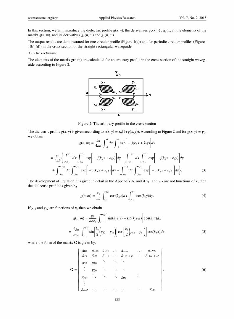
(a) (b)
(c) (d)
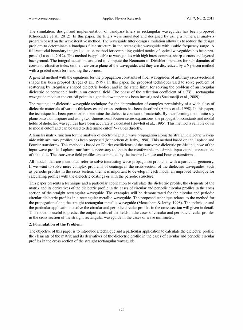
Figure 1. The circular profiles in the cross section of the straight waveguide (a) One circular profile. (b) Periodicstructure with two circular profiles along x-axis. (c) Periodic structure with two circular profiles along y-axis.
(d) Periodic structure with four circular profiles along x-axis and y-axis
Four examples of circular and periodic circular profiles in the cross section of the straight waveguide are shown inFigures 1(a)-(d). Figure 1(a) shows one circular profile where the center is located at the point (a/2, b/2). Figure1(b) shows an example of periodic structure with two circular profiles along x-axis. In this example, the center ofthe left circle is located at the point (a/4, b/2) and the center of the right circle is located at the point (3/4 a, b/2).
Figure 1(c) shows an example of periodic structure with two circular profiles along y-axis. In this example, thecenter of the upper circle is located at the point (a/2, 3/4 b) and the center of the lower circle is located at the point(a/2, b/4). Figure 1(d) shows an example of periodic structure with four circular profiles along x-axis and y-axis. Inthis example, the center of the first circle is located at the point (a/4, b/4), the center of the second circle is locatedat the point (3/4 a, b/4), the center of the third circle is located at the point (a/4 a, 3/4 b), and the center of the firthcircle is located at the point (3/4 a, 3/4 b).
The objective of this paper is to introduce a technique and a particular application to calculate the dielectric profile,the elements of the matrix and its derivatives of the dielectric profile in the cases of circular and periodic circularprofiles (Figures 1(a)-(d)) in the cross section of the straight rectangular waveguide. The proposed technique relatesto the method for the propagation along a straight rectangular metallic waveguide (Menachem & Jerby, 1998).The method is based on the Laplace and Fourier transforms, the inverse Laplace and Fourier transforms. Laplacetransform is necessary to obtain the comfortable and simple input-output connections of the fields. The outputtransverse field profiles are computed by the inverse Laplace and Fourier transforms. The output components of
123
www.ccsenet.org/apr Applied Physics Research Vol. 7, No. 2; 2015
the electric field are given finally by
Ex = {Dx + α1M1M2}−1 (Ex0 − α2M1Ey0 ), (1a)
Ey ={Dy + α1M3M4
}−1(Ey0 − α3M3Ex0 ), (1b)
Ez = Dz−1
{Ez0 +
12s
(GxEx0 +GyEy0 ) − 12
(GxEx +GyEy)}, (1c)
where Ex0 ,Ey0 ,Ez0 are the initial values of the corresponding fields at z=0, i.e., Ex0 = Ex (x, y, z=0), andEx0 , Ey0 , Ez0 are the initial-value vectors.
The modified wave-number matrices are given by
Dx ≡ K(0) +k2
oχ0
2sG +
jkox
2sNGx, Dy ≡ K(0) +
k2oχ0
2sG +
jkoy
2sMGy, Dz ≡ K(0) +
k2oχ0
2sG,
where the diagonal matrices K(0), M, and N are given by
(K(0))(n,m)(n′,m′) ={[
k2o − (nπ/a)2 − (mπ/b)2 + s2
]/2s
}δnn′δmm′ ,
M(n,m)(n′,m′) = mδnn′δmm′ , N(n,m)(n′,m′) = nδnn′δmm′ ,
and where
α1 =koxkoy
4s2 , α2 =jkox
2s, α3 =
jkoy
2s,
M1 = NGyDy−1, M2 =MGx, M3 =MGxDx
−1, M4 = NGy.
Similarly, the other components of the magnetic field are obtained. The output transverse field profiles are givenby the inverse Laplace and Fourier transforms, as follows
Ey(x, y, z) =∑
n
∑m
∫ σ+ j∞
σ− j∞Ey(n,m, s) exp
[jnkoxx + jmkoyy + sz
]ds, (2)
where the inverse Laplace transforms is calculated according to the Salzer method (Salzer, 1955) (Salzer, 1961). AFortran code is developed using NAG subroutines (The Numerical Algorithms Group (NAG)).
It is very interesting to compare between the mode model method for wave propagation in the straight waveguidewith a circular cross section (Menachem & Tapuchi, 2013) and this model for the wave propagation in the straightwaveguide with a rectangular cross section. These are two kinds of different methods that enable us to solvepractical problems with different boundary conditions. The calculations in all method are based on using Laplaceand Fourier transforms, and the output fields are computed by the inverse Laplace and Fourier transforms. Laplacetransform on the differential wave equations is needed to obtain the wave equations (and thus also the output fields)that are expressed directly as functions of the transmitted fields at the entrance of the waveguide at z = 0+. Thus,the Laplace transform is necessary to obtain the comfortable and simple input-output connections of the fields.
The technique and the particular application are proposed in the next section to calculate the dielectric profileg(x, y) and the derivatives gx(x, y) , gy(x, y) according to gx(x, y) = (1/ϵ(x, y))(dϵ(x, y)/dx) , ϵ(x, y) = ϵ0(1+ g(x, y)), and the elements of the matrix g(n,m), and its derivatives gx(n,m) and gy(n,m). The examples and the graphicalresults are given in the cases of circular and periodic circular profiles (Figures 1(a)-(d)) in the cross section of thestraight rectangular waveguide.
3. The Technique and the Particular Application
The technique, the particular application and several examples are demonstrated in this section in order to calculatethe dielectric profile and the derivatives of the dielectric profile in the cases of circular and periodic circular profiles,as shown in Figures 1(a)-(d).
124
www.ccsenet.org/apr Applied Physics Research Vol. 7, No. 2; 2015
In this section, we will introduce the dielectric profile g(x, y), the derivatives gx(x, y) , gy(x, y), the elements of thematrix g(n,m), and its derivatives gx(n,m) and gy(n,m).
The output results are demonstrated for one circular profile (Figure 1(a)) and for periodic circular profiles (Figures1(b)-(d)) in the cross section of the straight rectangular waveguide.
3.1 The Technique
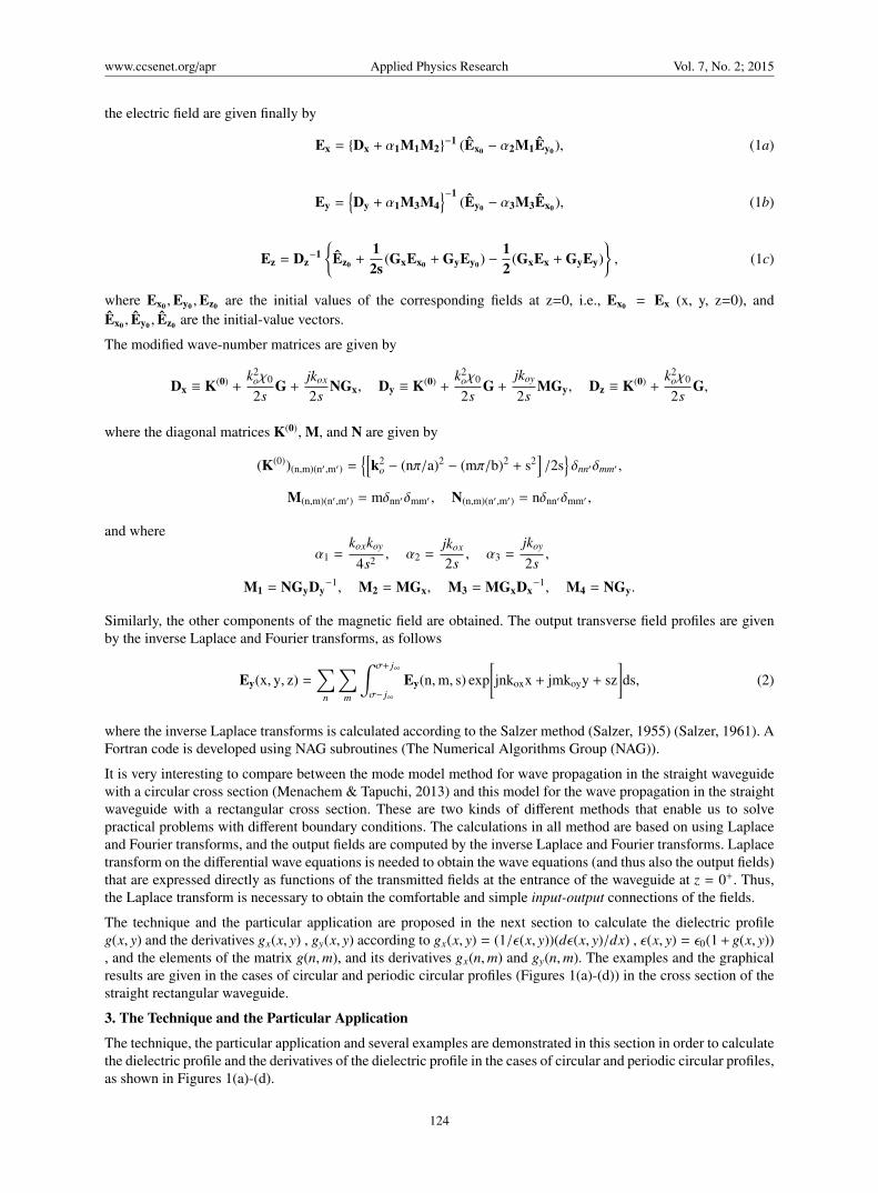
The elements of the matrix g(n,m) are calculated for an arbitrary profile in the cross section of the straight waveg-uide according to Figure 2.
Figure 2. The arbitrary profile in the cross section
The dielectric profile g(x, y) is given according to ϵ(x, y) = ϵ0(1+g(x, y)). According to Figure 2 and for g(x, y) = g0,we obtain
g(n,m) =g0
4ab
∫ a
−adx
∫ b
−bexp
[− j(kxx + kyy)
]dy
=g0
4ab
{∫ x12
x11
dx∫ y12
y11
exp[− j(kxx + kyy)
]dy +
∫ −x11
−x12
dx∫ y12
y11
exp[− j(kxx + kyy)
]dy
+
∫ −x11
−x12
dx∫ −y11
−y12
exp[− j(kxx + kyy)
]dy +
∫ x12
x11
dx∫ −y11
−y12
exp[− j(kxx + kyy)
]dy
}. (3)
The development of Equation 3 is given in detail in the Appendix A, and if y11 and y12 are not functions of x, thenthe dielectric profile is given by
g(n,m) =g0
ab
∫ x12
x11
cos(kxx)dx∫ y12
y11
cos(kyy)dy. (4)
If y11 and y12 are functions of x, then we obtain
g(n,m) =g0
abky
∫ x12
x11
[sin(kyy12) − sin(kyy11)
]cos(kxx)dx
=2g0
amπ
∫ x12
x11
sin[ky
2
(y12 − y11
)]cos
[ky
2
(y12 + y11
)]cos(kxx)dx, (5)
where the form of the matrix G is given by:
G =
g00 g−10 g−20 . . . g−nm . . . g−NM
g10 g00 g−10 . . . g−(n−1)m . . . g−(N−1)M
g20 g10. . .
. . .. . .
... g20. . .
. . .. . .
gnm. . .
. . .. . . g00
......
gNM . . . . . . . . . . . . . . . g00
. (6)
125
www.ccsenet.org/apr Applied Physics Research Vol. 7, No. 2; 2015
The derivative of the dielectric profile in the case of y11 and y12 are functions of x, is given by
gx(n,m) =2
amπ
∫ x12
x11
gx(x, y) sin[ky
2
(y12 − y11
)]cos
[ky
2
(y12 + y11
)]cos(kxx)dx, (7)
where gx(x, y) = (1/ϵ(x, y))(dϵ(x, y)/dx) , ϵ(x, y) = ϵ0(1 + g(x, y)) , kx = (nπx)/a, and ky = (mπy)/b. Similarly, wecan calculate the value of gx(n,m), where gy(x, y) = (1/ϵ(x, y))(dϵ(x, y)/dy).
The equation for one circle is given by (x − a/2)2 + (y − b/2)2 = r2, where the center of the circle is locatedat (a/2, b/2), as shown in Figure 1(a). Thus we obtain two possibilities y11(x) = b/2 −
√r2 − (x − a/2)2 and
y12(x) = b/2 +√
r2 − (x − a/2)2, according to Figure 2. In this case, we obtain y12 − y11 = 2√
r2 − (x − a/2)2 andy12 + y11 = b.
In the same principle we can calculate the equations for the periodic circles according to their location, as shownin Figures 1(b)-(d).
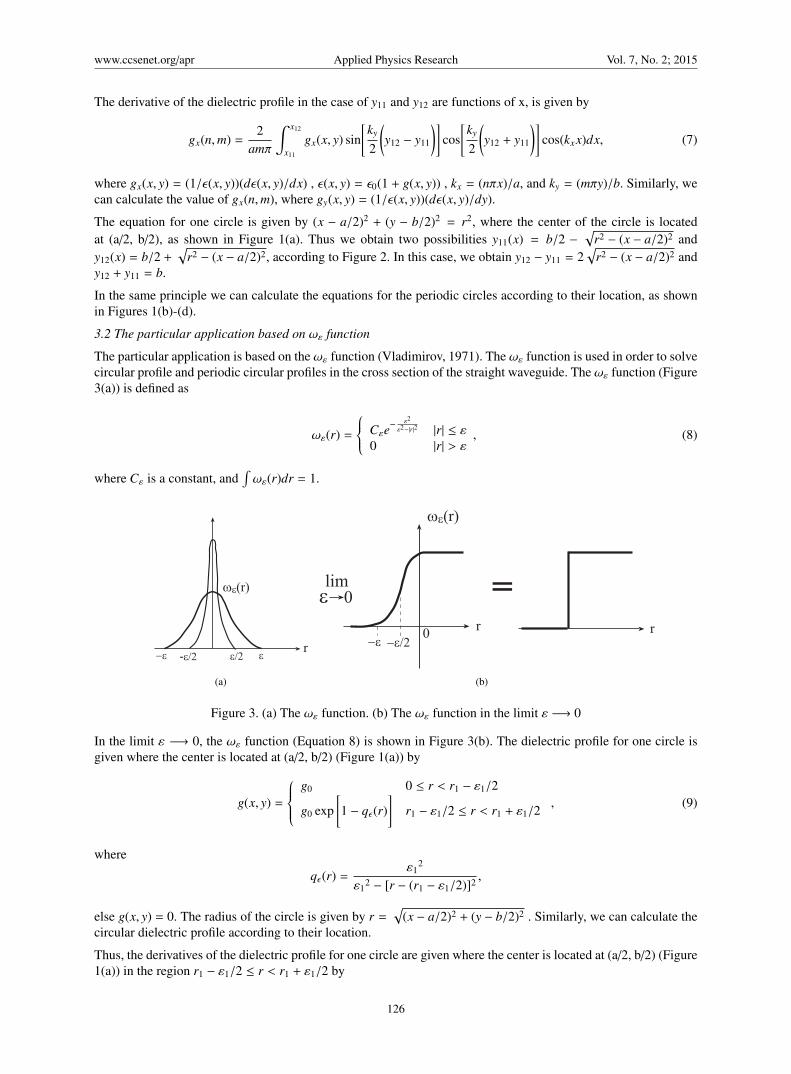
3.2 The particular application based on ωε function
The particular application is based on the ωε function (Vladimirov, 1971). The ωε function is used in order to solvecircular profile and periodic circular profiles in the cross section of the straight waveguide. The ωε function (Figure3(a)) is defined as
ωε(r) =
Cεe− ε2
ε2−|r|2 |r| ≤ ε0 |r| > ε
, (8)
where Cε is a constant, and∫ωε(r)dr = 1.
-e e
we(r)
r-e/2 e/2
(a)
-e
we(r)
=
0r r
lime 0
-e/2
(b)
Figure 3. (a) The ωε function. (b) The ωε function in the limit ε −→ 0
In the limit ε −→ 0, the ωε function (Equation 8) is shown in Figure 3(b). The dielectric profile for one circle isgiven where the center is located at (a/2, b/2) (Figure 1(a)) by
g(x, y) =
g0 0 ≤ r < r1 − ε1/2
g0 exp[1 − qϵ(r)
]r1 − ε1/2 ≤ r < r1 + ε1/2
, (9)
where
qϵ(r) =ε1
2
ε12 − [r − (r1 − ε1/2)]2 ,
else g(x, y) = 0. The radius of the circle is given by r =√
(x − a/2)2 + (y − b/2)2 . Similarly, we can calculate thecircular dielectric profile according to their location.
Thus, the derivatives of the dielectric profile for one circle are given where the center is located at (a/2, b/2) (Figure1(a)) in the region r1 − ε1/2 ≤ r < r1 + ε1/2 by
126
www.ccsenet.org/apr Applied Physics Research Vol. 7, No. 2; 2015
gx =
−2 g0 cos θ exp[1 − qϵ(r)
][r − (r1 − ε1/2)
]ε1
2
{1 + g0 exp
[1 − qϵ(r)
]}[ε1
2 − [r − (r1 − ε1/2)]2
]2 , (10a)
gy =
−2 g0 sin θ exp[1 − qϵ(r)
][r − (r1 − ε1/2)
]ε1
2
{1 + g0 exp
[1 − qϵ(r)
]}[ε1
2 − [r − (r1 − ε1/2)]2
]2 , (10b)
else gx =0, and gy =0.
The elements of the matrices for one circle are given where the center is located at (a/2, b/2) (Figure 1(a)) by
g(n,m) =g0
ab
{∫ 2π
0
∫ r1−ϵ1/2
0cos
[nπa
(r cos θ +a2
)]
cos[mπb
(r sin θ +b2
)]+
∫ 2π
0
∫ r1+ϵ1/2
r1−ϵ1/2cos
[nπa
(r cos θ +a2
)]
cos[mπb
(r sin θ +b2
)]
exp[1 − qϵ(r)
]}rdrdθ, (11)
gx(n,m) = −2g0
ab
{∫ 2π
0
∫ r1+ϵ1/2
r1−ϵ1/2
ϵ12[r − (r1 − ϵ1/2)] exp[1 − qϵ(r)] cos θ
[ϵ12 − [r − (r1 − ϵ1/2)]2]2[1 + g0 exp[1 − qϵ(r)]]
cos[nπa
(r cos θ +a2
)]
cos[mπb
(r sin θ +b2
)]}
rdrdθ, (12a)
gy(n,m) = −2g0
ab
{∫ 2π
0
∫ r1+ϵ1/2
r1−ϵ1/2
ϵ12[r − (r1 − ϵ1/2)] exp[1 − qϵ(r)] sin θ
[ϵ12 − [r − (r1 − ϵ1/2)]2]2[1 + g0 exp[1 − qϵ(r)]]
cos[nπa
(r cos θ +a2
)]
cos[mπb
(r sin θ +b2
)]}
rdrdθ, (12b)
where r =√
(x − a/2)2 + (y − b/2)2 .
Similarly, we can calculate the periodic circular profile according to the number of the circles and the locations oftheir centers.
4. Numerical Results
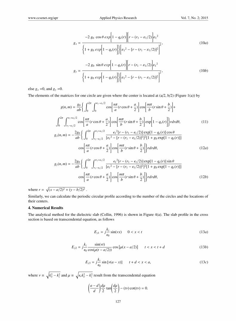
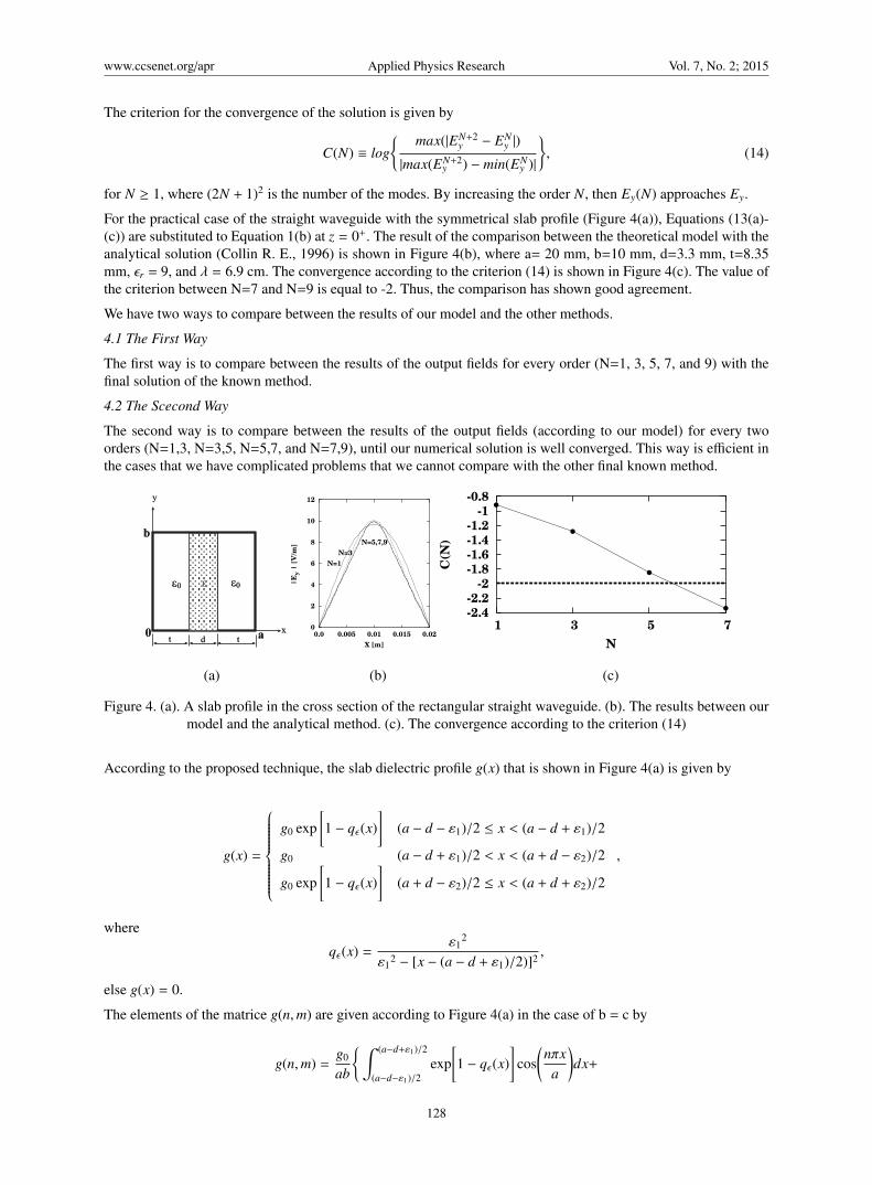
The analytical method for the dielectric slab (Collin, 1996) is shown in Figure 4(a). The slab profile in the crosssection is based on transcendental equation, as follows
Ey1 = jkz
ϵ0sin(νx) 0 < x < t (13a)
Ey2 = jkz
ϵ0
sin(νt)cos(µ(t − a/2))
cos[µ(x − a/2)
]t < x < t + d (13b)
Ey3 = jkz
ϵ0sin [ν(a − x)] t + d < x < a, (13c)
where ν ≡√
k2o − k2
z and µ ≡√ϵrk2
o − k2z result from the transcendental equation(a − d
d
)dµ2
tan(
dµ2
)− (tν) cot(tν) = 0.
127
www.ccsenet.org/apr Applied Physics Research Vol. 7, No. 2; 2015
The criterion for the convergence of the solution is given by
C(N) ≡ log{ max(|EN+2
y − ENy |)
|max(EN+2y ) − min(EN
y )|
}, (14)
for N ≥ 1, where (2N + 1)2 is the number of the modes. By increasing the order N, then Ey(N) approaches Ey.
For the practical case of the straight waveguide with the symmetrical slab profile (Figure 4(a)), Equations (13(a)-(c)) are substituted to Equation 1(b) at z = 0+. The result of the comparison between the theoretical model with theanalytical solution (Collin R. E., 1996) is shown in Figure 4(b), where a= 20 mm, b=10 mm, d=3.3 mm, t=8.35mm, ϵr = 9, and λ = 6.9 cm. The convergence according to the criterion (14) is shown in Figure 4(c). The value ofthe criterion between N=7 and N=9 is equal to -2. Thus, the comparison has shown good agreement.
We have two ways to compare between the results of our model and the other methods.
4.1 The First Way
The first way is to compare between the results of the output fields for every order (N=1, 3, 5, 7, and 9) with thefinal solution of the known method.
4.2 The Scecond Way
The second way is to compare between the results of the output fields (according to our model) for every twoorders (N=1,3, N=3,5, N=5,7, and N=7,9), until our numerical solution is well converged. This way is efficient inthe cases that we have complicated problems that we cannot compare with the other final known method.
y
xt td
b
a
e0 e0e
0
y
xt td
b
a
e0 e0e
0 0
2
4
6
8
10
12
0.0 0.005 0.01 0.015 0.02
|E
y |
[V
/m]
X [m]
N=1
N=3
N=5,7,9
-2.4-2.2
-2-1.8-1.6-1.4-1.2
-1-0.8
1 3 5 7
C(N
)
N
(a) (b) (c)
Figure 4. (a). A slab profile in the cross section of the rectangular straight waveguide. (b). The results between ourmodel and the analytical method. (c). The convergence according to the criterion (14)
According to the proposed technique, the slab dielectric profile g(x) that is shown in Figure 4(a) is given by
g(x) =
g0 exp
[1 − qϵ(x)
](a − d − ε1)/2 ≤ x < (a − d + ε1)/2
g0 (a − d + ε1)/2 < x < (a + d − ε2)/2
g0 exp[1 − qϵ(x)
](a + d − ε2)/2 ≤ x < (a + d + ε2)/2
,
where
qϵ(x) =ε1
2
ε12 − [x − (a − d + ε1)/2)]2 ,
else g(x) = 0.
The elements of the matrice g(n,m) are given according to Figure 4(a) in the case of b = c by
g(n,m) =g0
ab
{∫ (a−d+ε1)/2
(a−d−ε1)/2exp
[1 − qϵ(x)
]cos
(nπx
a
)dx+
128
www.ccsenet.org/apr Applied Physics Research Vol. 7, No. 2; 2015
∫ (a+d−ε2)/2
(a−d−ε1)/2cos
(nπx
a
)dx +
∫ (a+d+ε2)/2
(a+d−ε2)/2exp
[1 − qϵ(x)
]cos
(nπx
a
)dx
}{∫ b
0cos
(mπy
b
)dy
}.
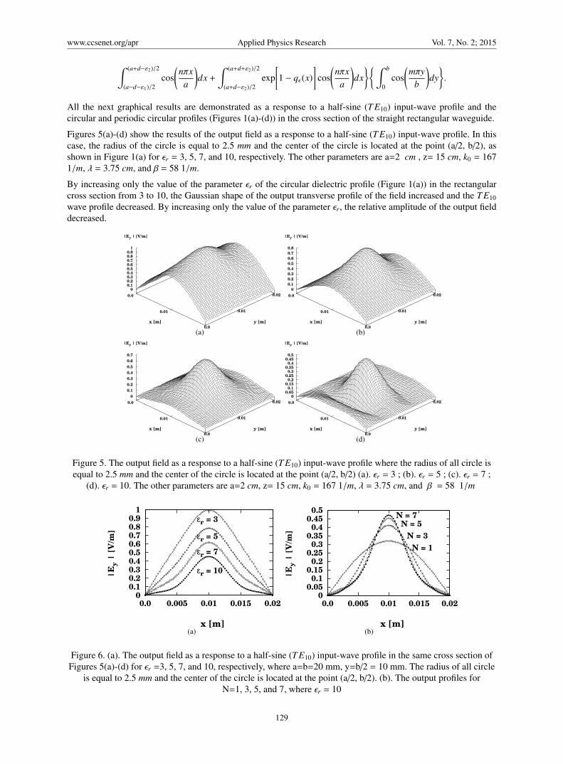
All the next graphical results are demonstrated as a response to a half-sine (T E10) input-wave profile and thecircular and periodic circular profiles (Figures 1(a)-(d)) in the cross section of the straight rectangular waveguide.
Figures 5(a)-(d) show the results of the output field as a response to a half-sine (T E10) input-wave profile. In thiscase, the radius of the circle is equal to 2.5 mm and the center of the circle is located at the point (a/2, b/2), asshown in Figure 1(a) for ϵr = 3, 5, 7, and 10, respectively. The other parameters are a=2 cm , z= 15 cm, k0 = 1671/m, λ = 3.75 cm, and β = 58 1/m.
By increasing only the value of the parameter ϵr of the circular dielectric profile (Figure 1(a)) in the rectangularcross section from 3 to 10, the Gaussian shape of the output transverse profile of the field increased and the T E10wave profile decreased. By increasing only the value of the parameter ϵr, the relative amplitude of the output fielddecreased.
0.01
0.0
x [m]
0.02
0.01
0.0
y [m]
0 0.1 0.2 0.3 0.4 0.5 0.6 0.7 0.8 0.9
1
|Ey | [V/m]
(a)
0.01
0.0
x [m]
0.02
0.01
0.0
y [m]
0
0.1
0.2
0.3
0.4
0.5
0.6
0.7
0.8
|Ey | [V/m]
(b)
0.01
0.0
x [m]
0.02
0.01
0.0
y [m]
0
0.1
0.2
0.3
0.4
0.5
0.6
0.7
|Ey | [V/m]
(c)
0.01
0.0
x [m]
0.02
0.01
0.0
y [m]
0 0.05 0.1
0.15 0.2
0.25 0.3
0.35 0.4
0.45 0.5
|Ey | [V/m]
(d)
Figure 5. The output field as a response to a half-sine (T E10) input-wave profile where the radius of all circle isequal to 2.5 mm and the center of the circle is located at the point (a/2, b/2) (a). ϵr = 3 ; (b). ϵr = 5 ; (c). ϵr = 7 ;
(d). ϵr = 10. The other parameters are a=2 cm, z= 15 cm, k0 = 167 1/m, λ = 3.75 cm, and β = 58 1/m
0 0.1 0.2 0.3 0.4 0.5 0.6 0.7 0.8 0.9
1
0.020.0150.010.0050.0
|E
y |
[V
/m]
x [m]
εr = 3
εr = 5
εr = 7
εr = 10
(a)
0 0.05 0.1
0.15 0.2
0.25 0.3
0.35 0.4
0.45 0.5
0.020.0150.010.0050.0
|E
y |
[V
/m]
x [m]
N = 1
N = 3
N = 5N = 7
(b)
Figure 6. (a). The output field as a response to a half-sine (T E10) input-wave profile in the same cross section ofFigures 5(a)-(d) for ϵr =3, 5, 7, and 10, respectively, where a=b=20 mm, y=b/2 = 10 mm. The radius of all circle
is equal to 2.5 mm and the center of the circle is located at the point (a/2, b/2). (b). The output profiles forN=1, 3, 5, and 7, where ϵr = 10
129
www.ccsenet.org/apr Applied Physics Research Vol. 7, No. 2; 2015
Figure 6(a) shows that by increasing only the value of ϵr of the circular dielectric profile, the Gaussian shape ofthe output field increased, the T E10 wave profile decreased, and the relative amplitude decreased. In addition, byincreasing only the value of ϵr, the width of the Gaussian shape decreased. The output profiles for N=1, 3, 5, and7 are shown in Figure 6(b) for ϵr = 10. The output field approaches to the final output field, by increasing only theparameter of the order N.
The output fields of Figures 5(a)-(d) and Figures 6(a)-(b) strongly affected by the input wave profile (T E10 mode),the circular profile, and the location of the center of the circle (a/2, b/2).
0.01
0.0
x [m]
0.02
0.01
0.0
y [m]
0 0.1 0.2 0.3 0.4 0.5 0.6 0.7 0.8 0.9
1
|Ey | [V/m]
(a)
0.01
0.0
x [m]
0.02
0.01
0.0
y [m]
0
0.2
0.4
0.6
0.8
1
1.2
1.4
|Ey | [V/m]
(b)
0.01
0.0
x [m]
0.02
0.01
0.0
y [m]
0
0.2
0.4
0.6
0.8
1
1.2
1.4
1.6
|Ey | [V/m]
(c)
0.01
0.0
x [m]
0.02
0.01
0.0
y [m]
0
0.2
0.4
0.6
0.8
1
1.2
1.4
1.6
|Ey | [V/m]
(d)
0
0.2
0.4
0.6
0.8
1
1.2
1.4
1.6
0.020.0150.010.0050.0
|E
y |
[V
/m]
x [m]
εr = 3
εr = 5εr = 7
εr = 10
(e)
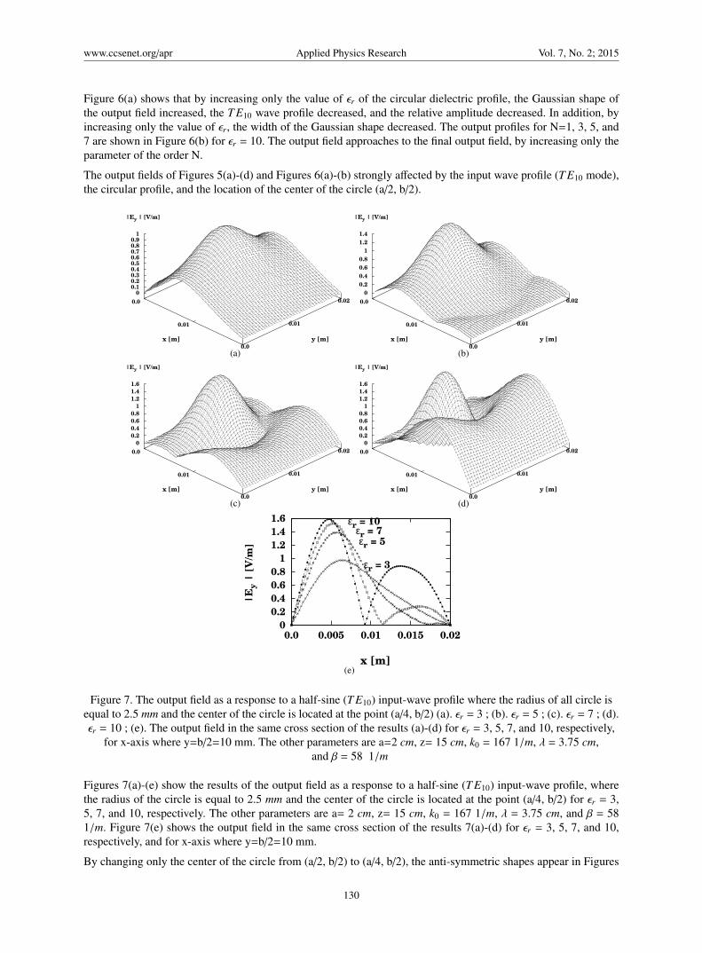
Figure 7. The output field as a response to a half-sine (T E10) input-wave profile where the radius of all circle isequal to 2.5 mm and the center of the circle is located at the point (a/4, b/2) (a). ϵr = 3 ; (b). ϵr = 5 ; (c). ϵr = 7 ; (d).ϵr = 10 ; (e). The output field in the same cross section of the results (a)-(d) for ϵr = 3, 5, 7, and 10, respectively,
for x-axis where y=b/2=10 mm. The other parameters are a=2 cm, z= 15 cm, k0 = 167 1/m, λ = 3.75 cm,and β = 58 1/m
Figures 7(a)-(e) show the results of the output field as a response to a half-sine (T E10) input-wave profile, wherethe radius of the circle is equal to 2.5 mm and the center of the circle is located at the point (a/4, b/2) for ϵr = 3,5, 7, and 10, respectively. The other parameters are a= 2 cm, z= 15 cm, k0 = 167 1/m, λ = 3.75 cm, and β = 581/m. Figure 7(e) shows the output field in the same cross section of the results 7(a)-(d) for ϵr = 3, 5, 7, and 10,respectively, and for x-axis where y=b/2=10 mm.
By changing only the center of the circle from (a/2, b/2) to (a/4, b/2), the anti-symmetric shapes appear in Figures
130
www.ccsenet.org/apr Applied Physics Research Vol. 7, No. 2; 2015
7(a)-(e). By increasing only the parameter ϵr from 3 to 10, the output field is dependent on the input wave profile(T E10 mode) and the Gaussian shape of circular dielectric profile. The output profiles (Figures 7(a)-(d)) are locatedin the left side with regards to the output profiles (Figures 5(a)-(d)), and the anti-symmetric shapes appear. Figure7(e) shows that by increasing only the value of ϵr of the circular dielectric profile, the anti-symmetric shapes appearthe output profiles and the amplitudes increasing.
The output fields (Figures 7(a)-(e)) strongly affected by the input wave profile (T E10 mode), the circular profile,and the location of the center of the circle (a/4, b/2).
0.01
0.0
x [m]
0.02
0.01
0.0
y [m]
0 0.1 0.2 0.3 0.4 0.5 0.6 0.7 0.8 0.9
1
|Ey | [V/m]
(a)
0.01
0.0
x [m]
0.02
0.01
0.0
y [m]
0
0.2
0.4
0.6
0.8
1
1.2
1.4
|Ey | [V/m]
(b)
0.01
0.0
x [m]
0.02
0.01
0.0
y [m]
0
0.2
0.4
0.6
0.8
1
1.2
1.4
1.6
|Ey | [V/m]
(c)
0.01
0.0
x [m]
0.02
0.01
0.0
y [m]
0
0.2
0.4
0.6
0.8
1
1.2
1.4
1.6
|Ey | [V/m]
(d)
0
0.2
0.4
0.6
0.8
1
1.2
1.4
1.6
0.020.0150.010.0050.0
|E
y |
[V
/m]
x [m]
εr = 3
εr = 5εr = 7εr = 10
(e)
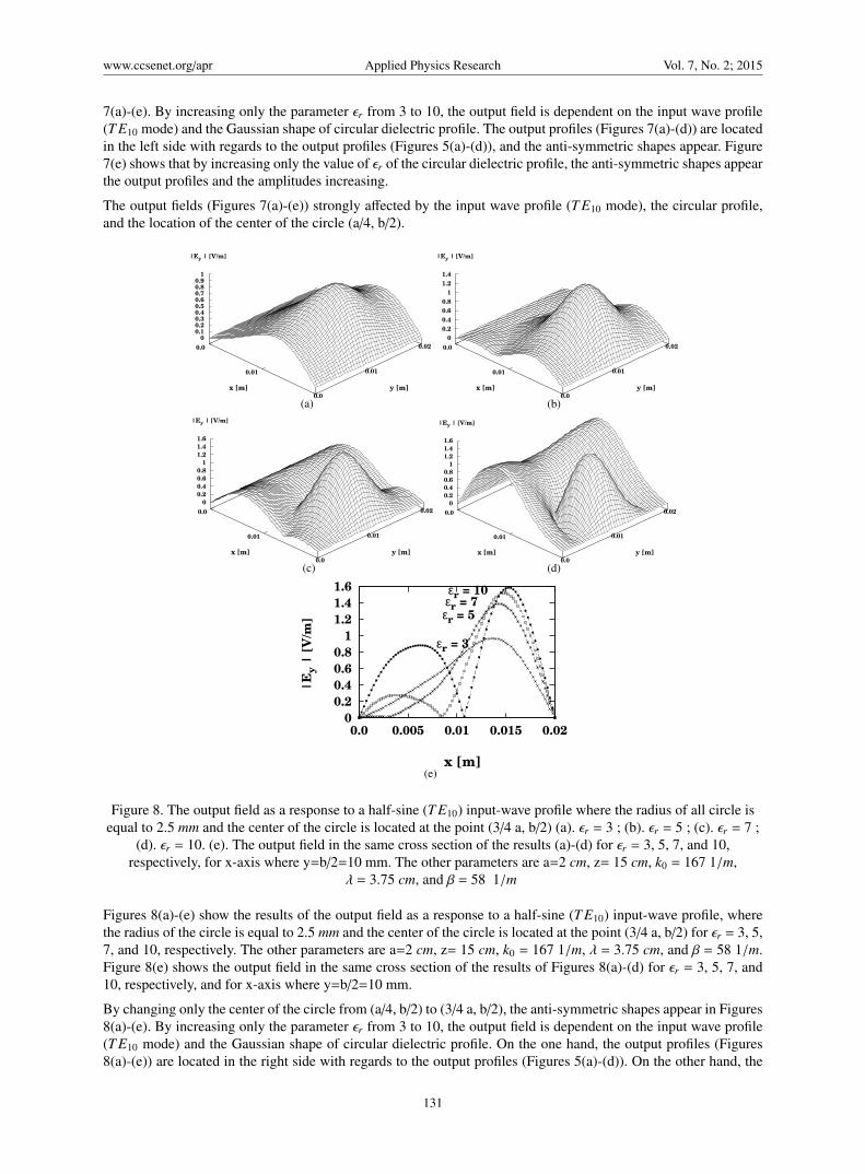
Figure 8. The output field as a response to a half-sine (T E10) input-wave profile where the radius of all circle isequal to 2.5 mm and the center of the circle is located at the point (3/4 a, b/2) (a). ϵr = 3 ; (b). ϵr = 5 ; (c). ϵr = 7 ;
(d). ϵr = 10. (e). The output field in the same cross section of the results (a)-(d) for ϵr = 3, 5, 7, and 10,respectively, for x-axis where y=b/2=10 mm. The other parameters are a=2 cm, z= 15 cm, k0 = 167 1/m,
λ = 3.75 cm, and β = 58 1/m
Figures 8(a)-(e) show the results of the output field as a response to a half-sine (T E10) input-wave profile, wherethe radius of the circle is equal to 2.5 mm and the center of the circle is located at the point (3/4 a, b/2) for ϵr = 3, 5,7, and 10, respectively. The other parameters are a=2 cm, z= 15 cm, k0 = 167 1/m, λ = 3.75 cm, and β = 58 1/m.Figure 8(e) shows the output field in the same cross section of the results of Figures 8(a)-(d) for ϵr = 3, 5, 7, and10, respectively, and for x-axis where y=b/2=10 mm.
By changing only the center of the circle from (a/4, b/2) to (3/4 a, b/2), the anti-symmetric shapes appear in Figures8(a)-(e). By increasing only the parameter ϵr from 3 to 10, the output field is dependent on the input wave profile(T E10 mode) and the Gaussian shape of circular dielectric profile. On the one hand, the output profiles (Figures8(a)-(e)) are located in the right side with regards to the output profiles (Figures 5(a)-(d)). On the other hand, the
131
www.ccsenet.org/apr Applied Physics Research Vol. 7, No. 2; 2015
output profiles (Figures 7(a)-(e)) are located in the left side with regards to the output profiles (Figures 5(a)-(d)).Figure 8(e) shows that by increasing only the value of ϵr of the circular dielectric profile, the anti-symmetric shapesappear, the output profiles and the amplitudes increasing. Note that the amplitude of the output field is not changedin the Figures 8(a)-(e) with regards to Figures 7(a)-(e), respectively, for the same value of ϵr.
The output fields (Figures 8(a)-(e)) strongly affected by the input wave profile (T E10 mode), the circular profile,and the location of the center of the circle (3/4 a, b/2).
0.01
0.0
x [m]
0.02
0.01
0.0
y [m]
0 0.1 0.2 0.3 0.4 0.5 0.6 0.7 0.8 0.9
1
|Ey | [V/m]
(a)
0.01
0.0
x [m]
0.02
0.01
0.0
y [m]
0 0.2 0.4 0.6 0.8
1 1.2 1.4 1.6 1.8
2
|Ey | [V/m]
(b)
0.01
0.0
x [m]
0.02
0.01
0.0
y [m]
0
0.5
1
1.5
2
2.5
3
|Ey | [V/m]
(c)
0.01
0.0
x [m]
0.02
0.01
0.0
y [m]
0
0.5
1
1.5
2
2.5
3
3.5
4
|Ey | [V/m]
(d)
0
0.2
0.4
0.6
0.8
1
1.2
0.020.0150.010.0050.0
|E
y |
[V
/m]
x [m]
εr = 3
εr = 5
εr = 7
εr = 10
(e)
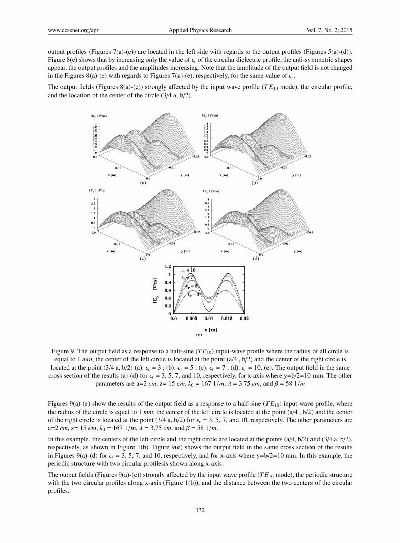
Figure 9. The output field as a response to a half-sine (T E10) input-wave profile where the radius of all circle isequal to 1 mm, the center of the left circle is located at the point (a/4 , b/2) and the center of the right circle is
located at the point (3/4 a, b/2) (a). ϵr = 3 ; (b). ϵr = 5 ; (c). ϵr = 7 ; (d). ϵr = 10. (e). The output field in the samecross section of the results (a)-(d) for ϵr = 3, 5, 7, and 10, respectively, for x-axis where y=b/2=10 mm. The other
parameters are a=2 cm, z= 15 cm, k0 = 167 1/m, λ = 3.75 cm, and β = 58 1/m
Figures 9(a)-(e) show the results of the output field as a response to a half-sine (T E10) input-wave profile, wherethe radius of the circle is equal to 1 mm, the center of the left circle is located at the point (a/4 , b/2) and the centerof the right circle is located at the point (3/4 a, b/2) for ϵr = 3, 5, 7, and 10, respectively. The other parameters area=2 cm, z= 15 cm, k0 = 167 1/m, λ = 3.75 cm, and β = 58 1/m.
In this example, the centers of the left circle and the right circle are located at the points (a/4, b/2) and (3/4 a, b/2),respectively, as shown in Figure 1(b). Figure 9(e) shows the output field in the same cross section of the resultsin Figures 9(a)-(d) for ϵr = 3, 5, 7, and 10, respectively, and for x-axis where y=b/2=10 mm. In this example, theperiodic structure with two circular profilesis shown along x-axis.
The output fields (Figures 9(a)-(e)) strongly affected by the input wave profile (T E10 mode), the periodic structurewith the two circular profiles along x-axis (Figure 1(b)), and the distance between the two centers of the circularprofiles.
132
www.ccsenet.org/apr Applied Physics Research Vol. 7, No. 2; 2015
0.01
0.0
x [m]
0.02
0.01
0.0
y [m]
0 0.1 0.2 0.3 0.4 0.5 0.6 0.7 0.8 0.9
1
|Ey | [V/m]
(a)
0.01
0.0
x [m]
0.02
0.01
0.0
y [m]
0
0.1
0.2
0.3
0.4
0.5
0.6
|Ey | [V/m]
(b)
0.01
0.0
x [m]
0.02
0.01
0.0
y [m]
0
0.05
0.1
0.15
0.2
0.25
0.3
0.35
0.4
|Ey | [V/m]
(c)
0.01
0.0
x [m]
0.02
0.01
0.0
y [m]
0
0.05
0.1
0.15
0.2
0.25
0.3
|Ey | [V/m]
(d)
0 0.1 0.2 0.3 0.4 0.5 0.6 0.7 0.8 0.9
0.020.0150.010.0050.0
|E
y |
[V
/m]
x [m]
εr = 3
εr = 5
εr = 7
εr = 10
(e)
0.1 0.2 0.3 0.4 0.5 0.6 0.7 0.8 0.9
1
0.020.0150.010.0050.0
|E
y |
[V
/m]
y [m]
εr = 3
εr = 5
εr = 7
εr = 10
(f)
Figure 10. The output field as a response to a half-sine (T E10) input-wave profile where the radius of all circle isequal to 2.5 mm, the center of the upper circle is located at the point (a/2 , 3/4 b) and the center of the lower circleis located at the point (a/2 a, b/4) for (a). ϵr = 3 ; (b). ϵr = 5 ; (c). ϵr = 7 ; (d). ϵr = 10. The output field in the samecross section of the same results (a)-(d) for ϵr = 3, 5, 7, and 10, respectively, for two cases: (e). for x-axis wherey=b/2=10 mm. (f). for y-axis where x=a/2=10 mm. The other parameters are a=2 cm, z= 15 cm, k0 = 167 1/m,
λ = 3.75 cm and β = 58 1/m
0.01
0.0
x [m]
0.02
0.01
0.0
y [m]
0 0.1 0.2 0.3 0.4 0.5 0.6 0.7 0.8 0.9
1
|Ey | [V/m]
(a)
0.01
0.0
x [m]
0.02
0.01
0.0
y [m]
0 0.1 0.2 0.3 0.4 0.5 0.6 0.7 0.8 0.9
|Ey | [V/m]
(b)
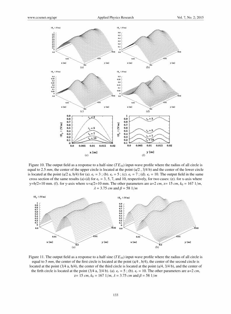
Figure 11. The output field as a response to a half-sine (T E10) input-wave profile where the radius of all circle isequal to 5 mm, the center of the first circle is located at the point (a/4 , b/4), the center of the second circle is
located at the point (3/4 a, b/4), the center of the third circle is located at the point (a/4, 3/4 b), and the center ofthe firth circle is located at the point (3/4 a, 3/4 b). (a). ϵr = 5 ; (b). ϵr = 10. The other parameters are a=2 cm,
z= 15 cm, k0 = 167 1/m, λ = 3.75 cm and β = 58 1/m
133
www.ccsenet.org/apr Applied Physics Research Vol. 7, No. 2; 2015
Figures 10(a)-(f) show the results of the output field as a response to a half-sine (T E10) input-wave profile for ϵr= 3, 5, 7, and 10, respectively. In this example, the radius of the circle is equal to 2.5 mm, the centers of the uppercircle and the lower circle are located at the points (a/2, 3/4 b) and (a/2, b/4), respectively, as shown in Figure 1(c).The other parameters are a=2 cm, z= 15 cm, k0 = 167 1/m, λ = 3.75 cm, and β = 58 1/m.
The output fields (Figures 10(a)-(f)) strongly affected by the input wave profile (T E10 mode), the periodic structurewith the two circular profiles along y-axis (Figure 1(c)), and the distance between the two centers of the circularprofiles.
The output fields in the same cross section of the results of Figures 10(a)-(d) are shown in Figure 10(e) for x-axis where y=b/2=10 mm and are shown in Figure 10(f) for y-axis where x=a/2=10 mm for ϵr=3, 5, 7, and 10,respectively. By changing only the parameter ϵr from 3 to 10, the relative profile of the output field is changedfrom a half-sine (T E10) profile to a Gaussian shape profile, as shown in Figure 10(e). The results of the periodicstructures of the output field along x-axis and y-axis are demonstrated in Figures 11(a)-(b). These results stronglyaffected by the half-sine (T E10) input-wave profile, the locations of the circular profiles along x-axis and alongy-axis (Figure 1(d)), and the distance between the fourth centers of the circular profiles.
Figures 11(a)-(b) show the results of the output field as a response to a half-sine (T E10) input-wave profile, wherethe radius of all circle is equal to 5 mm, the center of the first circle is located at the point (a/4 , b/4), the centerof the second circle is located at the point (3/4 a, b/4), the center of the third circle is located at the point (a/4, 3/4b), and the circle of the firth circle is located at the point (3/4 a, 3/4 b) for ϵr = 5, and 10, respectively. The otherparameters are a=2 cm, z= 15 cm, k0 = 167 1/m, λ = 3.75 cm, and β = 58 1/m.
The results of the periodic structures of the output field along x-axis and y-axis are demonstrated in Figures 11(a)-(b). These results strongly affected by the half-sine (T E10) input-wave profile, the locations of the circular profilesalong x-axis and along y-axis (Figure 1(d)), and the distance between the fourth centers of the circular profiles. Byincreasing the parameter ϵr from 5 to 10, the Gaussian shape of the output field increased.
5. Conclusions
The first objective of this paper was to present a technique and a particular application to calculate the dielectricprofile, the elements of the matrix, and its derivatives of the dielectric profile in the cases of circular and periodiccircular profiles in the cross section of the rectangular straight waveguide. The second objective was to investigatethe influence of the circular and periodic circular profiles on the output fields.
The technique was proposed in detail in order to understand how to calculate the elements of the matrix and itsderivatives. The output results were demonstrated for circular profile and for periodic circular profiles in the crosssection.
A comparison with the known transcendental equation was shown in order to examine the validity of the theoreticalmodel, by using with the proposed technique. The result of the comparison between the theoretical model with theknown solution (Collin, 1996) has shown good agreement.
All the graphical results were demonstrated as a response to a half-sine (T E10) input-wave profile and the circularand periodic circular profiles (Figures 1(a)-(d)) in the cross section of the straight rectangular waveguide. Thecalculation of the elements of the matrix g(n,m) for an arbitrary profile in the cross section of the straight waveguideis given according to Figure 2.
The results of the output field as a response to a half-sine (T E10) input-wave profile show that by increasing onlythe value of the parameter ϵr of the circular dielectric profile (Figure 1(a)) in the rectangular cross section from 3to 10, the Gaussian shape of the output transverse profile of the field increased, the T E10 wave profile decreased,and the width of the Gaussian shape decreased.
By changing only the center of the circle from (a/2, b/2) to (a/4, b/2), or by changing only the center of the circlefrom (a/4, b/2) to (3/4 a, b/2), the anti-symmetric shapes appear, the output profiles and the amplitudes increasing.
The results of the output fields strongly affected by the input wave profile (T E10 mode), the circular profile, andthe location of the center of the circle.
This model is useful to predict the structure of the output fields for circular and periodic circular profiles in a rect-angular metallic waveguide. The application is useful for straight waveguides in the microwave and the millimeter-wave regimes.
134
www.ccsenet.org/apr Applied Physics Research Vol. 7, No. 2; 2015
Appendix A
The dielectric profile g(x, y) is given according to ϵ(x, y) = ϵ0(1+g(x, y)). According to Figure 2 and for g(x, y) = g0,we obtain
g(n,m) =g0
4ab
∫ a
−adx
∫ b
−bexp
[− j(kxx + kyy)
]dy
=g0
4ab
{∫ x12
x11
dx∫ y12
y11
exp[− j(kxx + kyy)
]dy +
∫ −x11
−x12
dx∫ y12
y11
exp[− j(kxx + kyy)
]dy
+
∫ −x11
−x12
dx∫ −y11
−y12
exp[− j(kxx + kyy)
]dy +
∫ x12
x11
dx∫ −y11
−y12
exp[− j(kxx + kyy)
]dy
}
=g0
4ab
{∫ x12
x11
dx∫ y12
y11
exp[− j(kxx + kyy)
]dy +
∫ x11
x12
−dx∫ y12
y11
exp[− j(−kxx + kyy)
]dy
+
∫ x11
x12
−dx∫ y11
y12
− exp[− j(−kxx − kyy)
]dy +
∫ x12
x11
dx∫ y11
y12
− exp[− j(kxx − kyy)
]dy
}
=g0
4ab
{∫ x12
x11
exp[
j(kxx)]dx
∫ y12
y11
exp[
j(kyy)]dy +
∫ x12
x11
exp[
j(kxx)]dx
∫ y12
y11
exp[− j(kyy)
]dy
+
∫ x12
x11
exp[− j(kxx)
]dx
∫ y12
y11
exp[
j(kyy)]dy +
∫ x12
x11
exp[− j(kxx)
]dx
∫ y12
y11
exp[− j(kyy)
]dy
}
=g0
4ab
{∫ x12
x11
dx∫ y12
y11
exp[− j(kxx + kyy)
]dy +
∫ x12
x11
dx∫ y12
y11
exp[
j(kxx − kyy)]dy
+
∫ x12
x11
dx∫ y12
y11
exp[
j(kxx + kyy)]dy +
∫ x12
x11
dx∫ y12
y11
exp[− j(kxx − kyy)
]dy
}
=g0
2ab
{∫ x12
x11
(exp( jkxx) + exp(− jkxx)
)dx
∫ y12
y11
cos(kyy)dy}
.
References
Abbas, Z., Pollard, R. D. & Kelsall, W., (1998). A rectangular dielectric waveguide technique for determination ofpermittivity of materials at W-band. IEEE Transactions on Microwave Theory and Techniques, 46, 2011-2015.http://dx.doi.org/10.1109/22.739275
Choocadee, S., & Akatimagool, S. (2012). The simulation, design and implementation of bandpass filters in rectan-gular waveguides. Electrical and Electronic Engineering, 2, 152-157. http://dx.doi.org/10.5923/j.eee.20120203.08
Collin, R. E. (1996). Foundation for Microwave engineering. New York: McGraw-Hill.
Eyges, L., & Gianino, P. (1979). Modes of dielectric waveguides of arbitrary cross sectional shape. Journal Opt.Soc. Am., 69, 1226-1235. http://dx.doi.org/10.1364/JOSA.69.001226
Hewlett, S. J., & Ladouceur, F. (1995). Fourier decomposition method applied to mapped infinite domains: scalaranalysis of dielectric waveguides down to modal cutoff. Journal of Lightwave Technology, 13, 375-383.http://dx.doi.org/10.1109/50.372431
Jiao, C. Q. (2011). Selective suppression of electromagnetic modes in a rectangular waveguide by using distributedwall losses. Progress In Electromagnetics Research Letters, 22, 119-128.
Liu, S., Li, L. W., Leong, M. S., & Yeo, T. S. (2000). Rectangular conducting waveguide filled with uniaxialanisotropic media: a modal analysis and dyadic Green’s function. Progress In Electromagnetics Research, 25,111-129. http://dx.doi.org/10.2528/PIER99052501
135
www.ccsenet.org/apr Applied Physics Research Vol. 7, No. 2; 2015
Lu, W., & Lu, Y. Y. (2012). Waveguide mode solver based on Neumann-to-Dirichlet operators and boundary inte-gral equations. Journal of Computational Physics, 231, 1360-1371. http://dx.doi.org/10.1016/j.jcp.2011.10.016
Menachem, Z., & Jerby, E. (1998). Transfer Matrix Function (TMF) for propagation in dielectric waveguideswith arbitrary transverse profiles. IEEE Transactions On Microwave Theory and Techniques, 46, 975-982.http://dx.doi.org/10.1109/22.701451
Menachem, Z., & Tapuchi, S. (2013). Influence of the spot-size and cross-section on the output fields and powerdensity along the straight hollow waveguide. Progress In Electromagnetics Research, 48, 151-173. http://dx.doi.org/10.2528/PIERB12112009
Mineo, M., Carlo, A. Di., & Paoloni, C. (2010). Analytical design method for corrugated rectangular waveguideSWS THZ vacuum tubes. Journal of Electromagnetic Waves and Applications, 24, 2479-2494. http://dx.doi.org/10.1163/156939310793675745
Rothwell, E. J., Temme, A., & Crowgey, B. (2009). Pulse reflection from a dielectric discontinuity in a rectangularwaveguide. Progress In Electromagnetics Research, 97, 11-25. http://dx.doi.org/10.2528/PIER09090905
Salzer, H. E. (1955). Orthogonal polynomials arising in the numerical evaluation of inverse Laplace transforms.Math. Tables and Other Aids to Comut., 9, 164-177. http://dx.doi.org/10.2307/2002053
Salzer, H. E. (1961). Additional formulas and tables for orthogonal polynomials originating from inversion inte-grals. J. Math. Phys., 39, 72-86.
Sharma, J. (2010). Full-wave analysis of dielectric rectangular waveguides. Progress In Electromagnetics Re-search, 13, 121-131. http://dx.doi.org/10.2528/PIERM10051802
Soekmadji, H., Liao, S. L., & Vernon, R. J. (2009). Experiment and simulation on T E10 cut-off reflection phase ingentle rectangular downtapers. Progress In Electromagnetics Research Letters, 12, 79-85. http://dx.doi.org/10.2528/PIERL09090707
Vladimirov, V. S., Jeffrey, A., & Littlewood, A. (1971). Equations of Mathematical Physics (pp. 66-67). New York:M. Dekker.
Yeap, K. H., Tham, C. Y., Yassin, G., & Yeong, K. C. (2011). Attenuation in rectangular waveguides with finiteconductivity walls. Radioengineering, 20, 472-478.
Copyrights
Copyright for this article is retained by the author(s), with first publication rights granted to the journal.
This is an open-access article distributed under the terms and conditions of the Creative Commons Attributionlicense (http://creativecommons.org/licenses/by/3.0/).
136