Embed Size (px)
Citation preview
Circuits and Systems for Efficient
Portable-to-Portable Wireless Charging
by
Rui Jin
S.B., Massachusetts Institute of Technology (2013)
Submitted to the Department of Electrical Engineering and ComputerScience
in Partial Fulfillment of the Requirements for the Degree of
Master of Engineering in Electrical Engineering and Computer Science
at the
MASSACHUSETTS INSTITUTE OF TECHNOLOGY
June 2014
c© Massachusetts Institute of Technology 2014. All rights reserved.
Author . . . . . . . . . . . . . . . . . . . . . . . . . . . . . . . . . . . . . . . . . . . . . . . . . . . . . . . . . . . . . . . . . .Department of Electrical Engineering and Computer Science
May 2, 2014
Certified by . . . . . . . . . . . . . . . . . . . . . . . . . . . . . . . . . . . . . . . . . . . . . . . . . . . . . . . . . . . . . .Anantha P. Chandrakasan
Joseph F. and Nancy P. Keithley Professor of Electrical EngineeringThesis Supervisor
Accepted by . . . . . . . . . . . . . . . . . . . . . . . . . . . . . . . . . . . . . . . . . . . . . . . . . . . . . . . . . . . . .Albert R. Meyer
Chairman, Masters of Engineering Thesis Committee

2
Circuits and Systems for Efficient
Portable-to-Portable Wireless Charging
by
Rui Jin
Submitted to the Department of Electrical Engineering and Computer Scienceon May 2, 2014, in partial fulfillment of the
requirements for the degree ofMaster of Engineering in Electrical Engineering and Computer Science
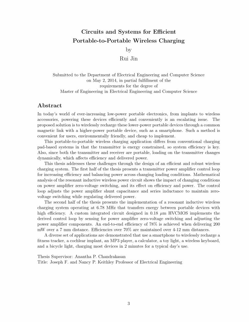
Abstract
In today’s world of ever-increasing low-power portable electronics, from implants to wirelessaccessories, powering these devices efficiently and conveniently is an escalating issue. Theproposed solution is to wirelessly recharge these lower-power portable devices through a commonmagnetic link with a higher-power portable device, such as a smartphone. Such a method isconvenient for users, environmentally friendly, and cheap to implement.
This portable-to-portable wireless charging application differs from conventional chargingpad-based systems in that the transmitter is energy constrained, so system efficiency is key.Also, since both the transmitter and receiver are portable, loading on the transmitter changesdynamically, which affects efficiency and delivered power.
This thesis addresses these challenges through the design of an efficient and robust wirelesscharging system. The first half of the thesis presents a transmitter power amplifier control loopfor increasing efficiency and balancing power across changing loading conditions. Mathematicalanalysis of the resonant inductive wireless power circuit shows the impact of changing conditionson power amplifier zero-voltage switching, and its effect on efficiency and power. The controlloop adjusts the power amplifier shunt capacitance and series inductance to maintain zero-voltage switching while regulating delivered power.
The second half of the thesis presents the implementation of a resonant inductive wirelesscharging system operating at 6.78 MHz that transfers energy between portable devices withhigh efficiency. A custom integrated circuit designed in 0.18 µm HVCMOS implements thederived control loop by sensing for power amplifier zero-voltage switching and adjusting thepower amplifier components. An end-to-end efficiency of 78% is achieved when delivering 200mW over a 7 mm distance. Efficiencies over 70% are maintained over 4-12 mm distances.
A diverse set of applications are demonstrated that use a smartphone to wirelessly recharge afitness tracker, a cochlear implant, an MP3 player, a calculator, a toy light, a wireless keyboard,and a bicycle light, charging most devices in 2 minutes for a typical day’s use.
Thesis Supervisor: Anantha P. ChandrakasanTitle: Joseph F. and Nancy P. Keithley Professor of Electrical Engineering
3

Acknowledgments
I am deeply grateful to so many people who helped me get to the place I am today and taughtme invaluable lessons along the way. It has been my dream since childhood to come to MIT. Iam indebted to all the people who have not only helped me realize this dream but also givenme experiences beyond all my imaginations. As I child I thought of this school as a place ofmagic, and looking back at my years here I again think this is a magical place.
I would like to thank my research advisor, Prof. Anantha Chandrakasan, for his guidanceand support over the past four years. When I first joined his group as a second-year under-graduate student, I knew virtually nothing about circuits, and through his mentorship and thediverse set of projects he encouraged me to work on, he taught me so many things I know now.Anantha taught me not only about circuit design but also about how to approach researchproblems, how to focus on the major questions, and how to communicate ideas to others. Hehas been central to my undergrad research experience at MIT, which I love so much and whichI think is one of the most important aspects that sets MIT apart.
I would like to thank my first research advisor, Prof. Vincent Chan, who introduced me tothe wonderful world of research and saw my interest in circuit design when I was clueless. Whenhe connected me with Anantha, Vincent told me that in our first meeting Anantha would “pullout a bucket of water and ask you to swim.” While Anantha has helped me swim in severalbuckets through the years, Vincent helped me get into the first one, and through his vision Ihave gotten to where I am.
I would like to thank a few incredibly talented researchers that I have been fortunate tohave worked with and have taught me so much. I’d like to thank Marcus Yip, whose boundlessknowledge and unending patience have made this research and thesis possible, through thehours he spent discussing the circuits in my project and teaching me how to use the designsoftware, and through the advice he gave me as my graduate student mentor. I started workingwith him as an undergrad, and doing research with him was one of the major reasons I decidedto stay and pursue my Master’s degree. I am honored to have been his mentee, glad to behis friend, and excited to work with him in the future. I’d like to thank Nathan Ickes, whohas guided me through research ever since my first project in Anantha’s group. He has taughtme countless things about circuits and is always willing to teach me more. I’d like to thankNachiket Desai, who gave me invaluable guidance on core theories in this thesis. I really enjoyedour interactions, whether they were technical meetings or casual conversations.
I would like to thank Tina Stankovic and Don Eddington at the Massachusetts Eye and EarInfirmary for making time in their busy schedules to help make the cochlear implant applicationfor wireless charging a success. They brought a whole new clinical perspective to the electronicsI worked on, which has broadened my focus and made me think about exactly what work ismeaningful.
I would like to thank all the brilliant students in Ananthagroup, who have become somethingof a family to me over the past few years. They are the brightest, nicest, and most amazinggroup of people I have ever met. What I will remember forever are the incredible experiences Ihad, from random technical conversations in the lab to badminton games on weekends to movieoutings at school.
I would like to thank Margaret Flaherty for keeping the lab running as we were breaking itdown with our experiments. She works harder than any of us, and it makes our work so mucheasier.
I would like to thank Yihui Qiu from Foxconn for her advice and support, and the greatconversations we had at her house parties. I would like to thank the TSMC University Shuttle
4

Program for chip fabrication support.I would like to thank my classmates and friends I have met at MIT. Ben, Bryan, Carrie,
Devon, James, Joey, Lisa, Pon, Qian, Sharon, Stephan, Stephen, Theresa, thanks for the besttime of my life and I will remember our laughs even after I’ve forgotten everything else.
I would like to thank my Mom and Dad for making all of this possible. You two believed inme even when I did not and it is your love and encouragement and persistence that makes measpire to fulfill my dreams. My new dream is to raise my children like you raised me.
5

Contents
1 Introduction 131.1 Current Wireless Power Technologies . . . . . . . . . . . . . . . . . . . . . . . . 141.2 Motivation for Wireless Charging of Portable Electronics . . . . . . . . . . . . . 151.3 Vision for Portable-to-Portable Wireless Charging . . . . . . . . . . . . . . . . . 17
1.3.1 Representative Use Cases for Portable-to-Portable Wireless Charging . . 171.3.2 User Metrics for Portable-to-Portable Wireless Charging . . . . . . . . . 18
1.4 Thesis Contributions and Organization . . . . . . . . . . . . . . . . . . . . . . . 19
2 Basic Wireless Charging Circuits 212.1 Basic Wireless Charging System Block Diagram . . . . . . . . . . . . . . . . . . 212.2 Basic Wireless Charging Circuit . . . . . . . . . . . . . . . . . . . . . . . . . . . 22
2.2.1 Operating Frequency . . . . . . . . . . . . . . . . . . . . . . . . . . . . . 232.2.2 Coil Sizes and Inductances . . . . . . . . . . . . . . . . . . . . . . . . . . 232.2.3 Coupling Coefficient . . . . . . . . . . . . . . . . . . . . . . . . . . . . . 24
2.3 Basic Wireless Charging Circuit Performance . . . . . . . . . . . . . . . . . . . 252.3.1 Rectifier Equivalent Resistance . . . . . . . . . . . . . . . . . . . . . . . 252.3.2 Primary-Side Equivalent Resistance . . . . . . . . . . . . . . . . . . . . 252.3.3 Delivered Power . . . . . . . . . . . . . . . . . . . . . . . . . . . . . . . 262.3.4 Efficiency . . . . . . . . . . . . . . . . . . . . . . . . . . . . . . . . . . . 26
2.4 Basic Power Amplifier Circuit . . . . . . . . . . . . . . . . . . . . . . . . . . . . 272.5 Chapter Summary . . . . . . . . . . . . . . . . . . . . . . . . . . . . . . . . . . 28
3 Design Overview and Previous Work 293.1 Wireless Charging System Design Overview . . . . . . . . . . . . . . . . . . . . 29
3.1.1 Design Challenges . . . . . . . . . . . . . . . . . . . . . . . . . . . . . . 293.1.2 Design Objectives . . . . . . . . . . . . . . . . . . . . . . . . . . . . . . 303.1.3 Design Overview . . . . . . . . . . . . . . . . . . . . . . . . . . . . . . . 31
3.2 Previous Implementations of Wireless Power Systems . . . . . . . . . . . . . . . 323.2.1 Lo et al., IEEE Biomedical Circuits and Systems 2013 [1] . . . . . . . . 323.2.2 Kendir et al., IEEE Circuits and Systems 2005 [2] . . . . . . . . . . . . 333.2.3 Baker, Sarpeshkar, IEEE Biomedical Circuits and Systems 2007 [3] . . . 333.2.4 Wang et al., IEEE Circuits and Systems 2005 [4] . . . . . . . . . . . . . 34
3.3 Chapter Summary . . . . . . . . . . . . . . . . . . . . . . . . . . . . . . . . . . 35
4 Power Amplifier Control Loop for High Efficiency and Balanced Power 364.1 Block-Level Efficiency Breakdown . . . . . . . . . . . . . . . . . . . . . . . . . . 364.2 Power Amplifier and Wireless Link Analysis Strategy . . . . . . . . . . . . . . . 38
6
4.3 Effect of Power Amplifier Zero-Voltage Switching on Efficiency . . . . . . . . . 384.4 Effect of Changing Conditions on Equivalent Resistance . . . . . . . . . . . . . 404.5 Maintaining Power Amplifier Full ZVS . . . . . . . . . . . . . . . . . . . . . . . 424.6 Maintaining Power Amplifier General ZVS . . . . . . . . . . . . . . . . . . . . . 434.7 Power Amplifier Control Loop Design . . . . . . . . . . . . . . . . . . . . . . . 444.8 Meeting the Design Objectives . . . . . . . . . . . . . . . . . . . . . . . . . . . 474.9 Simulation Results . . . . . . . . . . . . . . . . . . . . . . . . . . . . . . . . . . 48
4.9.1 Effects of Changing Conditions and Compensation on ZVS . . . . . . . 494.9.2 End-to-End Efficiency and Delivered Power of Dynamic vs. Fixed Systems 51
4.10 Summary of Theoretical Analysis of Design for Efficiency and Power . . . . . . 52
5 Adaptive Wireless Charging Integrated Circuit Design 535.1 Wireless Charging Controller Microchip Block Design . . . . . . . . . . . . . . . 535.2 Microchip Power Amplifier Switch Drive Buffer Design . . . . . . . . . . . . . . 545.3 Microchip Pulse Generator Block Design . . . . . . . . . . . . . . . . . . . . . . 55
5.3.1 Ring Oscillator Design . . . . . . . . . . . . . . . . . . . . . . . . . . . . 555.3.2 Pulse Extractor Design . . . . . . . . . . . . . . . . . . . . . . . . . . . . 56
5.4 Microchip Analog Block Design . . . . . . . . . . . . . . . . . . . . . . . . . . . 575.4.1 Zero-Volt Comparator Design . . . . . . . . . . . . . . . . . . . . . . . . 575.4.2 V REF Comparator Design . . . . . . . . . . . . . . . . . . . . . . . . . 58
5.5 Microchip Digital Block Design . . . . . . . . . . . . . . . . . . . . . . . . . . . 585.5.1 Range-Determination Digital Logic Design . . . . . . . . . . . . . . . . . 595.5.2 Compensation-Determination Digital Logic Design . . . . . . . . . . . . 59
5.6 Microchip Timing . . . . . . . . . . . . . . . . . . . . . . . . . . . . . . . . . . . 615.7 Microchip Switch Block Design . . . . . . . . . . . . . . . . . . . . . . . . . . . 625.8 Chapter Summary . . . . . . . . . . . . . . . . . . . . . . . . . . . . . . . . . . 64
6 Adaptive Wireless Charging System Design 656.1 Wireless Power Circuit Implementation . . . . . . . . . . . . . . . . . . . . . . . 66
6.1.1 Class-E Power Amplifier Implementation . . . . . . . . . . . . . . . . . . 666.1.2 Wireless Link Implementation . . . . . . . . . . . . . . . . . . . . . . . . 676.1.3 Rectifier Implementation . . . . . . . . . . . . . . . . . . . . . . . . . . . 686.1.4 Load Implementation . . . . . . . . . . . . . . . . . . . . . . . . . . . . 696.1.5 Wireless Power Circuit Implementation Summary . . . . . . . . . . . . . 69
6.2 Wireless Charging Control Chip Implementation . . . . . . . . . . . . . . . . . 696.2.1 Chip Supplies . . . . . . . . . . . . . . . . . . . . . . . . . . . . . . . . . 706.2.2 Chip Inputs . . . . . . . . . . . . . . . . . . . . . . . . . . . . . . . . . . 706.2.3 Chip Outputs . . . . . . . . . . . . . . . . . . . . . . . . . . . . . . . . . 70
6.3 Accessory Circuit Implementation . . . . . . . . . . . . . . . . . . . . . . . . . . 706.3.1 1.8 V V DD Buck Converter Implementation . . . . . . . . . . . . . . . 706.3.2 6.78 MHz Oscillator Implementation . . . . . . . . . . . . . . . . . . . . 71
6.4 Board Design Considerations . . . . . . . . . . . . . . . . . . . . . . . . . . . . 716.4.1 Isolation to Transmit and Receive Coils . . . . . . . . . . . . . . . . . . 726.4.2 Undesired Inductance of Transmit and Receive Coils . . . . . . . . . . . 72
6.5 Chapter Summary . . . . . . . . . . . . . . . . . . . . . . . . . . . . . . . . . . 73
7
7 Implementation and Measurement Results 747.1 Chip Implementation . . . . . . . . . . . . . . . . . . . . . . . . . . . . . . . . . 747.2 Test System Implementation . . . . . . . . . . . . . . . . . . . . . . . . . . . . . 757.3 Power Amplifier Control Loop Operation . . . . . . . . . . . . . . . . . . . . . . 767.4 Efficiency and Power Measurement Results and Discussion . . . . . . . . . . . . 787.5 Comparison to Previous Work . . . . . . . . . . . . . . . . . . . . . . . . . . . . 827.6 Prototype System Implementation . . . . . . . . . . . . . . . . . . . . . . . . . 837.7 Chip and System Limitations . . . . . . . . . . . . . . . . . . . . . . . . . . . . 847.8 Summary of Wireless Charging Integrated Circuit and System Design and Im-
plementation . . . . . . . . . . . . . . . . . . . . . . . . . . . . . . . . . . . . . 86
8 Portable-to-Portable Wireless Charging Applications 878.1 Toys - Toy Light . . . . . . . . . . . . . . . . . . . . . . . . . . . . . . . . . . . 888.2 Wearable Devices - Fitbit Fitness Tracker . . . . . . . . . . . . . . . . . . . . . 898.3 Medical Devices - Cochlear Implant . . . . . . . . . . . . . . . . . . . . . . . . . 918.4 Media Devices - iPod Shuffle . . . . . . . . . . . . . . . . . . . . . . . . . . . . . 928.5 Wireless Accessories - Wireless Keyboard . . . . . . . . . . . . . . . . . . . . . 938.6 AA / AAA-Battery Operated Devices - Graphing Calculator . . . . . . . . . . 948.7 Coin Cell Battery-Operated Devices - Bicycle Light . . . . . . . . . . . . . . . . 958.8 Chapter Summary . . . . . . . . . . . . . . . . . . . . . . . . . . . . . . . . . . 96
9 Conclusions and Future Directions 979.1 Summary of Contributions . . . . . . . . . . . . . . . . . . . . . . . . . . . . . . 979.2 Towards a Power Sharing Vision . . . . . . . . . . . . . . . . . . . . . . . . . . 99
A Details of Class-E Power Amplifier Operation 102A.1 Effect of Changing Coupling and Output Voltage on Equivalent Resistance . . . 103A.2 Effect of Changing Equivalent Resistance on Power Amplifier Operation in Full
ZVS . . . . . . . . . . . . . . . . . . . . . . . . . . . . . . . . . . . . . . . . . . 104A.2.1 Derivation of v(wt) in Full ZVS Condition . . . . . . . . . . . . . . . . . 105A.2.2 Derivation of LEX in Full ZVS Condition . . . . . . . . . . . . . . . . . 106A.2.3 Derivation of CP in Full ZVS Condition . . . . . . . . . . . . . . . . . . 106
A.3 Effect of Changing Equivalent Resistance on Power Amplifier Operation in Gen-eral ZVS . . . . . . . . . . . . . . . . . . . . . . . . . . . . . . . . . . . . . . . . 107A.3.1 Analysis of v(wt) in General ZVS Condition . . . . . . . . . . . . . . . . 108A.3.2 Decomposition of v(wt) in General ZVS Condition . . . . . . . . . . . . 109A.3.3 Analysis of v(wt) in General ZVS Condition . . . . . . . . . . . . . . . . 110A.3.4 Overall Analysis of General ZVS Condition . . . . . . . . . . . . . . . . 110
A.4 Simulation Results . . . . . . . . . . . . . . . . . . . . . . . . . . . . . . . . . . 116
B Wireless Charging Controller Chip Pinout 119
8

List of Figures
1.1 Overview of current wireless power technologies . . . . . . . . . . . . . . . . . . 141.2 Power sharing structure for portable-to-portable wireless charging . . . . . . . 17
2.1 Block diagram of the basic wireless charging system . . . . . . . . . . . . . . . . 212.2 Circuit-level diagram of the basic wireless charging system . . . . . . . . . . . . 222.3 Coupling coefficient variation with separation for 30 mm / 25 mm coils . . . . . 242.4 Basic wireless charging circuit with equivalent output resistance . . . . . . . . . 252.5 Primary-side equivalent circuit for power transfer . . . . . . . . . . . . . . . . . 262.6 Basic Class-E power amplifier circuit . . . . . . . . . . . . . . . . . . . . . . . . 272.7 Class-E power amplifier waveforms . . . . . . . . . . . . . . . . . . . . . . . . . 27
3.1 Adaptive wireless charging system general diagram . . . . . . . . . . . . . . . . 31
4.1 Simulation setup for block-level efficiency analysis . . . . . . . . . . . . . . . . . 374.2 Class-E power amplifier switch drain voltage waveform cases . . . . . . . . . . . 394.3 Basic wireless power circuit . . . . . . . . . . . . . . . . . . . . . . . . . . . . . 404.4 REQ versus coupling coefficient k . . . . . . . . . . . . . . . . . . . . . . . . . . 414.5 REQ versus output voltage VOUT . . . . . . . . . . . . . . . . . . . . . . . . . . 414.6 Class-E power amplifier circuit . . . . . . . . . . . . . . . . . . . . . . . . . . . 424.7 XP
RPRI+REQvs. S in general ZVS . . . . . . . . . . . . . . . . . . . . . . . . . . . 43
4.8 XEX
RPRI+REQvs. S in general ZVS . . . . . . . . . . . . . . . . . . . . . . . . . . . 44
4.9 Received power variations in general ZVS condition . . . . . . . . . . . . . . . . 464.10 Switch drain voltage for L1 = 5 uH, CP = 80 pF system, k = 0.2, VOUT = 3.8 V
conditions . . . . . . . . . . . . . . . . . . . . . . . . . . . . . . . . . . . . . . . 494.11 Switch drain voltage for L1 = 5 uH, CP = 80 pF system, k = 0.15, VOUT = 3.8
V conditions . . . . . . . . . . . . . . . . . . . . . . . . . . . . . . . . . . . . . . 494.12 Switch drain voltage for L1 = 4.9 uH, CP = 160 pF system, k = 0.15, VOUT = 3.8
V conditions . . . . . . . . . . . . . . . . . . . . . . . . . . . . . . . . . . . . . . 504.13 Simulated end-to-end efficiency and delivered power of dynamic vs. fixed systems 51
5.1 Wireless charging controller microchip block diagram . . . . . . . . . . . . . . . 535.2 Ring oscillator schematic diagram . . . . . . . . . . . . . . . . . . . . . . . . . . 555.3 Leakage-based inverter schematic diagram . . . . . . . . . . . . . . . . . . . . . 555.4 Pulse extractor schematic diagram . . . . . . . . . . . . . . . . . . . . . . . . . 565.5 Zero-volt comparator circuit design . . . . . . . . . . . . . . . . . . . . . . . . . 575.6 V REF comparator circuit design . . . . . . . . . . . . . . . . . . . . . . . . . . 585.7 Range-determination digital logic schematic . . . . . . . . . . . . . . . . . . . . 595.8 Compensation-determination digital logic schematic for setting A . . . . . . . . 59
9

5.9 Compensation-determination digital logic schematic for setting Z . . . . . . . . 605.10 Drive buffer, pulse generator, analog block, and digital block timing diagram . . 615.11 Tunable power amplifier shunt capacitance schematic diagram . . . . . . . . . . 625.12 Tunable resonant tank inductance schematic diagram . . . . . . . . . . . . . . . 63
6.1 Full wireless charging system diagram . . . . . . . . . . . . . . . . . . . . . . . 656.2 Transmit and receive coil design . . . . . . . . . . . . . . . . . . . . . . . . . . . 676.3 Trace routing to transmit coil . . . . . . . . . . . . . . . . . . . . . . . . . . . . 73
7.1 Chip die photo . . . . . . . . . . . . . . . . . . . . . . . . . . . . . . . . . . . . 747.2 System test board . . . . . . . . . . . . . . . . . . . . . . . . . . . . . . . . . . 757.3 Dynamic outputs of test system chip . . . . . . . . . . . . . . . . . . . . . . . . 767.4 Power amplifier switch drain voltage waveform for d = 8 mm, VOUT = 4 V . . . 777.5 Power amplifier switch drain voltage waveform for d = 10 mm, VOUT = 4 V . . 777.6 Power amplifier switch drain voltage waveform for d = 13 mm, VOUT = 4 V . . 777.7 Measured end-to-end efficiency results vs. other systems . . . . . . . . . . . . . 787.8 Measured delivered power results vs. fixed system . . . . . . . . . . . . . . . . . 797.9 Measured efficiency breakdown . . . . . . . . . . . . . . . . . . . . . . . . . . . 807.10 Power consumption breakdown at 7 mm charging distance . . . . . . . . . . . . 817.11 Specification comparison to previous published work and commercial products . 827.12 Prototype system transmitter board . . . . . . . . . . . . . . . . . . . . . . . . 84
8.1 General receiver circuit for applications . . . . . . . . . . . . . . . . . . . . . . . 878.2 Wireless charging system for a toy light display . . . . . . . . . . . . . . . . . . 888.3 Wireless charging system for a Fitbit fitness tracker . . . . . . . . . . . . . . . . 898.4 Wireless charging receiver for a cochlear implant . . . . . . . . . . . . . . . . . 918.5 Wireless charging receiver for an iPod Shuffle . . . . . . . . . . . . . . . . . . . 928.6 Wireless charging receiver for a wireless keyboard . . . . . . . . . . . . . . . . . 938.7 Wireless charging receiver for a graphing calculator . . . . . . . . . . . . . . . . 948.8 Wireless charging receiver for a bicycle light . . . . . . . . . . . . . . . . . . . . 95
9.1 Body area network for data and power transfer . . . . . . . . . . . . . . . . . . 99
A.1 Class-E power amplifier circuit . . . . . . . . . . . . . . . . . . . . . . . . . . . 102A.2 Switch voltage waveform with full ZVS condition . . . . . . . . . . . . . . . . . 104A.3 Switch voltage waveform with general ZVS condition . . . . . . . . . . . . . . . 108A.4 φ vs. S in general ZVS . . . . . . . . . . . . . . . . . . . . . . . . . . . . . . . . 113A.5 |VS | and |VEX | vs. S in general ZVS . . . . . . . . . . . . . . . . . . . . . . . . 114A.6 XEX
RPRI+REQvs. S in general ZVS . . . . . . . . . . . . . . . . . . . . . . . . . . . 115
A.7 XP
RPRI+REQvs. S in general ZVS . . . . . . . . . . . . . . . . . . . . . . . . . . . 115
A.8 Switch drain voltage for L1 = 5 uH, CP = 80 pF system, k = 0.25, VOUT = 3.8V conditions . . . . . . . . . . . . . . . . . . . . . . . . . . . . . . . . . . . . . . 116
A.9 Switch drain voltage for L1 = 5.1 uH, CP = 50 pF system, k = 0.25, VOUT = 3.8V conditions . . . . . . . . . . . . . . . . . . . . . . . . . . . . . . . . . . . . . . 116
A.10 Switch drain voltage for L1 = 5 uH, CP = 80 pF system, k = 0.2, VOUT = 5 Vconditions . . . . . . . . . . . . . . . . . . . . . . . . . . . . . . . . . . . . . . . 117
A.11 Switch drain voltage for L1 = 4.9 uH, CP = 160 pF system, k = 0.2, VOUT = 5V conditions . . . . . . . . . . . . . . . . . . . . . . . . . . . . . . . . . . . . . . 117
10

A.12 Switch drain voltage for L1 = 5 uH, CP = 80 pF system, k = 0.2, VOUT = 3 Vconditions . . . . . . . . . . . . . . . . . . . . . . . . . . . . . . . . . . . . . . . 117
A.13 Switch drain voltage for L1 = 5.1 uH, CP = 50 pF system, k = 0.2, VOUT = 3 Vconditions . . . . . . . . . . . . . . . . . . . . . . . . . . . . . . . . . . . . . . . 118
B.1 Chip pinout diagram . . . . . . . . . . . . . . . . . . . . . . . . . . . . . . . . . 119
11

List of Tables
1.1 Representative use cases for portable-to-portable wireless charging . . . . . . . 18
2.1 Summary of basic parameters used in this work . . . . . . . . . . . . . . . . . . 28
3.1 Design objectives for wireless charging system in this work . . . . . . . . . . . . 313.2 Comparison of this system design approach to previous approaches . . . . . . . 35
4.1 Tunable excess inductance and shunt capacitance values used in design . . . . . 47
5.1 Tunable excess inductance and shunt capacitance values used in design . . . . . 60
6.1 Shunt capacitance values used in testing . . . . . . . . . . . . . . . . . . . . . . 676.2 Wireless power circuit components used in testing . . . . . . . . . . . . . . . . . 69
8.1 Summary of wireless charging receiver applications . . . . . . . . . . . . . . . . 96
B.1 Description of wireless charging controller pinout . . . . . . . . . . . . . . . . . 120
12

Chapter 1
Introduction
Since the 1800s when inventors harnessed electricity for the first telegraphs and light bulbs, de-
velopment of modern electronics has relied on the availability and abundance of energy sources.
These electronics operate with power delivered at appropriate times, whether it’s from an AC-
DC adapter to perform a computation in a processor or from a transmission line to spin an
electric motor. In many cases, power is transferred to the device through conductive wire, such
as through the cables of the AC-DC adapter or the lines of the transmission grid.
Wireless power transfer is an old technology with new popularity. Its roots can be traced
back to Nikola Tesla, who demonstrated in the late 1800s that light bulbs could be powered
through wireless coupling of energy from giant high-voltage coils. At the time, wirelessly pow-
ered devices existed only in Tesla’s private labs and public lectures. Today, many products
exist and much research is being undertaken relating to many implementations of wireless
power transfer, at a variety of power levels from micro-watts to kilowatts.
13
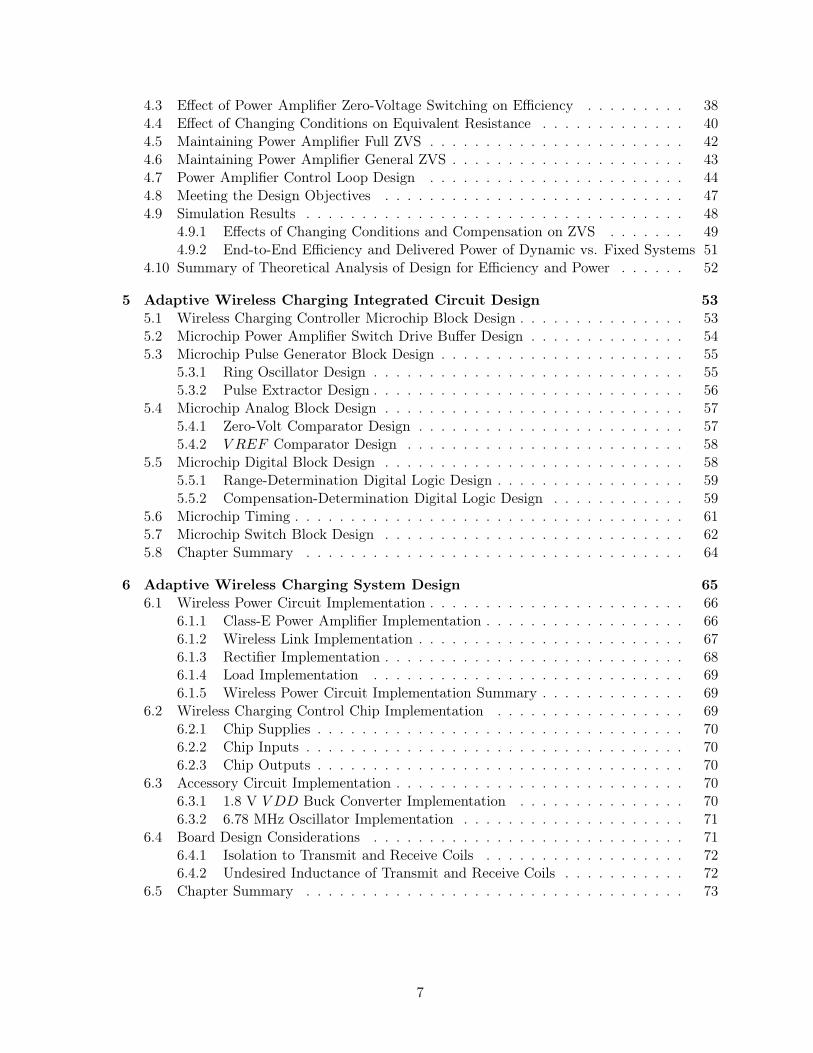
1.1 Current Wireless Power Technologies
Figure 1.1: Overview of current wireless power technologies
Figure 1.1 shows the range of wireless power technologies currently being explored in both the
commercial and academic arenas, over a wide range of power levels [5, 6, 7, 8, 4, 9].
On the low-power end, many medical implants rely on wireless power to function. One
example is the cochlear implant, a device with implanted electrodes that stimulate auditory
nerves to promote hearing [5]. According to the Food and Drug Administration, as of December
2012, about 324,000 people worldwide have received these devices [10]. Each implant is coupled
through a magnet to a power transmitter outside the ear, which transfers milliwatts of power
wirelessly through the skin. Researchers are also developing retinal implants that stimulate
electrodes in the eye to promote sight [4]. These medical devices require on the order of 100 mW
of wirelessly transmitted power. Outside the medical space, researchers are also investigating
systems to wirelessly charge lithium ion batteries at 10 mW rates [8].
In the middle of the power spectrum, many commercial products are on the market today
that provide wireless power for popular consumer electronics such as cell phones and tablets.
One example is the Duracell Powermat, which is a charging pad plugged into an electrical
outlet that recharges compatible consumer devices placed on top [6]. Devices such as cell
phones may be outfitted with a special case to support wireless recharging. Another example
14
are the WiTricity charging pad products to transfer power to cell phones and tablets. WiTricity
repeaters can be used to extend the wireless power range to charge devices from father away
[11].
These products are among many similar ones that adhere to specific industry standards
for wireless power transfer at about 1-10 W levels. One such standard is the Power Matters
Alliance, with members such as WiTricity, Duracell, and Qualcomm [12]. Another standard is
the Wireless Power Consortium, or Qi, with members such as Texas Instruments, Energizer,
and Panasonic [13]. Both standards cover resonant wireless power transfer with applications
such as charging mobile devices on a charging pad over distances on the order of 1 cm.
On the high-power end, at about 1 kW levels, people in both academia and industry are
developing technologies to power large machines. At CES 2011, Fulton Innovation demonstrated
the technology to wirelessly charge batteries in an electric vehicle [7]. Researchers are studying
system designs for higher efficiency power transfer to wafer processing machines [9].
1.2 Motivation for Wireless Charging of Portable Electronics
Given all the wireless power technologies currently in existence operating at various power
levels, there is at least one power level regime that has not been heavily explored: the low-to-mid
power region between 100 mW and 1 W. Many consumer portable electronics can be recharged
at these levels, from wireless accessories, such as wireless keyboards, to AA(A) battery-operated
devices, such as graphing calculators, to medical implants, such as cochlear implants or pace-
makers.
These portable electronics are used on a daily basis, and thus need to be recharged regu-
larly. But the current methods of recharging portable electronics are both inconvenient and
environmentally unfriendly. Users either charge the device through a charging cable or directly
recharge the batteries inside the device, and both of these methods involve external equipment
(cables or chargers) not built into the portable that must be carried with the portable. This
may be a hassle for users. In the case of medical implants, regularly wearing external equipment
to charge or power these implants could be a source of social stigma as well. In addition, at
the end of life, this external equipment contributes to a large amount of environmental waste,
15
including 179,000 tons of waste batteries and 51,000 tons of waste chargers per year in the
United States [14, 15].
At the same time, companies and researchers are rapidly developing wireless power technolo-
gies for ubiquitous mobile devices such as cell phones and tablets, hence the industry standards
described earlier. The wireless power circuitry in these higher-power portable devices could not
only be used as receivers to charge these devices, but also as transmitters to charge lower-power
portable devices.
A system that wirelessly recharges portable electronics using a higher-power mobile device is
both convenient for users and environmentally friendly. The hassle of carrying external charging
equipment is eliminated as portable devices would have a built-in common wireless interface
with a mobile device for transferring power. As a result, associated waste is also eliminated. The
system is also a convenient and relatively stigma-free solution for charging medical implants.
A wireless charging system using a higher-power mobile device is relatively cheap to im-
plement relative to the cost of current charging methods. If the higher-power mobile device is
already part of another system that wirelessly charges the mobile device, then the device only
needs to be outfitted with a power amplifier and control logic circuits to transmit power to other
portable devices. In essence the only added costs and electronics of the proposed system would
be in the receiver portable devices. Today, people in the United States spend an estimated
10.6 billion dollars yearly on secondary lead-acid batteries to power portable devices, or about
twenty dollars per person per year [16]. Considering that the proposed system involves only
circuit-level additions to already-existing electronics, this price point is not difficult to beat.
16
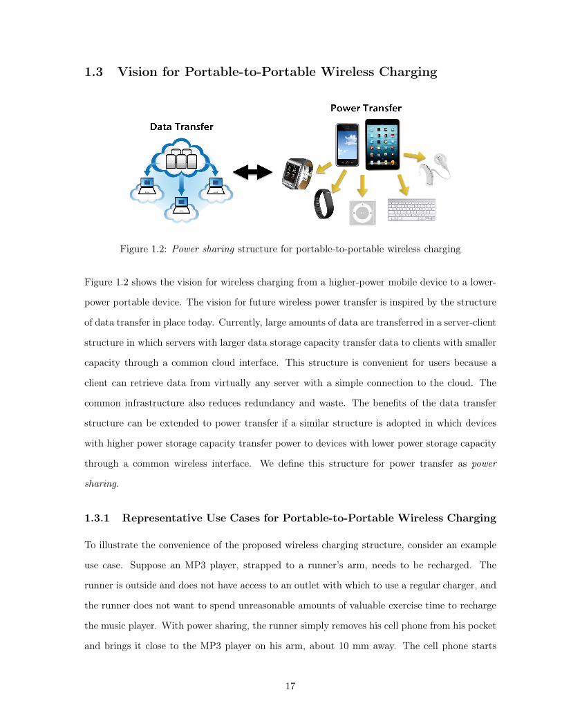
1.3 Vision for Portable-to-Portable Wireless Charging
Figure 1.2: Power sharing structure for portable-to-portable wireless charging
Figure 1.2 shows the vision for wireless charging from a higher-power mobile device to a lower-
power portable device. The vision for future wireless power transfer is inspired by the structure
of data transfer in place today. Currently, large amounts of data are transferred in a server-client
structure in which servers with larger data storage capacity transfer data to clients with smaller
capacity through a common cloud interface. This structure is convenient for users because a
client can retrieve data from virtually any server with a simple connection to the cloud. The
common infrastructure also reduces redundancy and waste. The benefits of the data transfer
structure can be extended to power transfer if a similar structure is adopted in which devices
with higher power storage capacity transfer power to devices with lower power storage capacity
through a common wireless interface. We define this structure for power transfer as power
sharing.
1.3.1 Representative Use Cases for Portable-to-Portable Wireless Charging
To illustrate the convenience of the proposed wireless charging structure, consider an example
use case. Suppose an MP3 player, strapped to a runner’s arm, needs to be recharged. The
runner is outside and does not have access to an outlet with which to use a regular charger, and
the runner does not want to spend unreasonable amounts of valuable exercise time to recharge
the music player. With power sharing, the runner simply removes his cell phone from his pocket
and brings it close to the MP3 player on his arm, about 10 mm away. The cell phone starts
17
transferring power wirelessly to the MP3 player, taking about 2 minutes to charge. Afterwards,
the runner can use the newly recharged MP3 player for the rest of his exercise routine.
As another example use case, suppose a person has a cochlear implant. With a conventional
implant, she needs to wear a set of external equipment to constantly stream power to her
implant. This equipment may not be waterproof, thus preventing her from engaging in water
sports or limiting usage in the shower. This external equipment is bulky and thus may contribute
to social stigma. With power sharing, she no longer needs to wear this external equipment.
Instead, she uses her cell phone to wirelessly recharge her implant in the morning in a couple
minutes for an entire day’s usage. Her cochlear implant is now truly invisible.
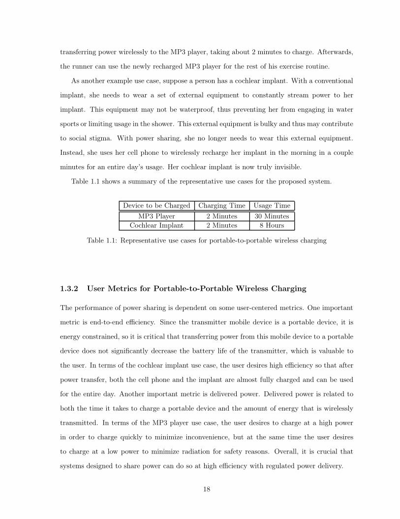
Table 1.1 shows a summary of the representative use cases for the proposed system.
Device to be Charged Charging Time Usage Time
MP3 Player 2 Minutes 30 Minutes
Cochlear Implant 2 Minutes 8 Hours
Table 1.1: Representative use cases for portable-to-portable wireless charging
1.3.2 User Metrics for Portable-to-Portable Wireless Charging
The performance of power sharing is dependent on some user-centered metrics. One important
metric is end-to-end efficiency. Since the transmitter mobile device is a portable device, it is
energy constrained, so it is critical that transferring power from this mobile device to a portable
device does not significantly decrease the battery life of the transmitter, which is valuable to
the user. In terms of the cochlear implant use case, the user desires high efficiency so that after
power transfer, both the cell phone and the implant are almost fully charged and can be used
for the entire day. Another important metric is delivered power. Delivered power is related to
both the time it takes to charge a portable device and the amount of energy that is wirelessly
transmitted. In terms of the MP3 player use case, the user desires to charge at a high power
in order to charge quickly to minimize inconvenience, but at the same time the user desires
to charge at a low power to minimize radiation for safety reasons. Overall, it is crucial that
systems designed to share power can do so at high efficiency with regulated power delivery.
18

1.4 Thesis Contributions and Organization
This work develops circuits and systems that work towards the wireless power sharing vision
and that help realize the use cases described in Subsection 1.3.1. The main contributions are
in the following three areas:
1. Transmitter power amplifier control loop for high efficiency and regulated
power: Chapters 2-4 present a theoretical analysis of the wireless power system to de-
rive a transmitter-side power amplifier control loop for increasing system efficiency and
balancing delivered power over changing conditions. Chapter 2 gives an introduction to
wireless power transfer. Chapter 3 describes the general control loop design, highlights
the objectives it satisfies, and compares it to previous work. The main design challenge is
the variability of portable-to-portable wireless charging coupling and loading conditions,
and the control loop addresses this through dynamic compensation of the power amplifier
components. Chapter 4 provides control loop design details. The design is motivated by
a detailed analysis of the efficiency and delivered power of a conventional wireless power
transfer system over changing conditions. The analysis shows that power amplifier zero-
voltage switching is critical to high efficiency, and this leads to a method adopted in the
control loop of dynamic feedback and adjustment of the power amplifier shunt capacitance
and resonant tank series inductance to maintain zero-voltage switching while balancing
delivered power. Mathematical analysis is supported by simulation results.
2. Integrated circuit and system design for wireless charging: Chapters 5-7 present
a full design of a wireless charging system incorporating the power amplifier control loop.
Chapter 5 presents the design of an ultra low-power integrated circuit in 0.18 µm HVC-
MOS that implements the control loop by sensing for power amplifier zero-voltage switch-
ing and dynamically adjusting the power amplifier component values. Chapter 6 provides
the design of the board-level transmitter and receiver subsystems that use the fabricated
integrated circuit in a functioning resonant inductive wireless charger system operating
at 6.78 MHz. Chapter 7 provides measurement results. The system achieves 78% peak
end-to-end efficiency transferring 200 mW over 7 mm, and achieves over 70% end-to-end
efficiency transferring about 200 mW over 4-12 mm distances.
19

3. Medical, sensor, and consumer applications for portable-to-portable wireless
charging: Chapter 8 presents seven system applications for portable-to-portable wireless
charging, from medical devices such as a fully-implantable cochlear implant to sensor
devices such as a fitness tracker to niche devices such as bicycle light. Each application
is developed to support wireless recharging of the associated portable device using a
smartphone in 2-15 mins for a typical day’s usage. The applications showcase the wide-
ranging opportunities for power sharing.
Wireless power sharing from device to device will dramatically improve users’ experiences with
portable electronics and contribute to greater environmental sustainability.
20
Chapter 2
Basic Wireless Charging Circuits
Before detailing the new techniques in this thesis, this chapter first presents a background
in wireless power circuit basics. The following chapters build on these conventional circuits to
improve performance in the key user metrics of high efficiency and consistent delivered power.
2.1 Basic Wireless Charging System Block Diagram
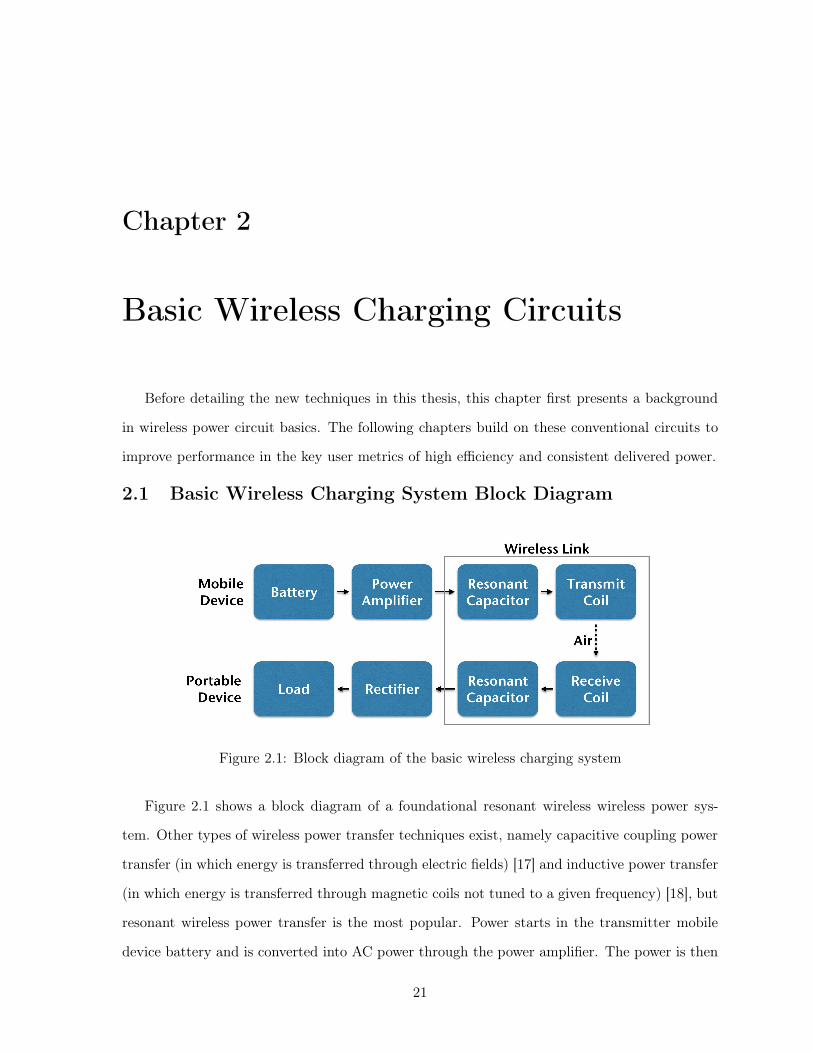
Figure 2.1: Block diagram of the basic wireless charging system
Figure 2.1 shows a block diagram of a foundational resonant wireless wireless power sys-
tem. Other types of wireless power transfer techniques exist, namely capacitive coupling power
transfer (in which energy is transferred through electric fields) [17] and inductive power transfer
(in which energy is transferred through magnetic coils not tuned to a given frequency) [18], but
resonant wireless power transfer is the most popular. Power starts in the transmitter mobile
device battery and is converted into AC power through the power amplifier. The power is then
21
delivered into the wireless link, which consists essentially of two coupled resonant tanks, the
primary-side resonant tank in the transmitter device and the secondary-side resonant tank in
the receiver device. Each resonant tank includes a capacitor in series with a matched inductor,
which is implemented in this case as a discrete coil. Power is transferred through the air between
these two coupled coils. The received AC power is then rectified and is available to charge the
portable device battery and power a load.
2.2 Basic Wireless Charging Circuit
−vAC
+
PA Output
RS
R1 C1
iPRI
L1 L2
k:n
iSEC
C2R2
iOUT
COUT
+vOUT− Load
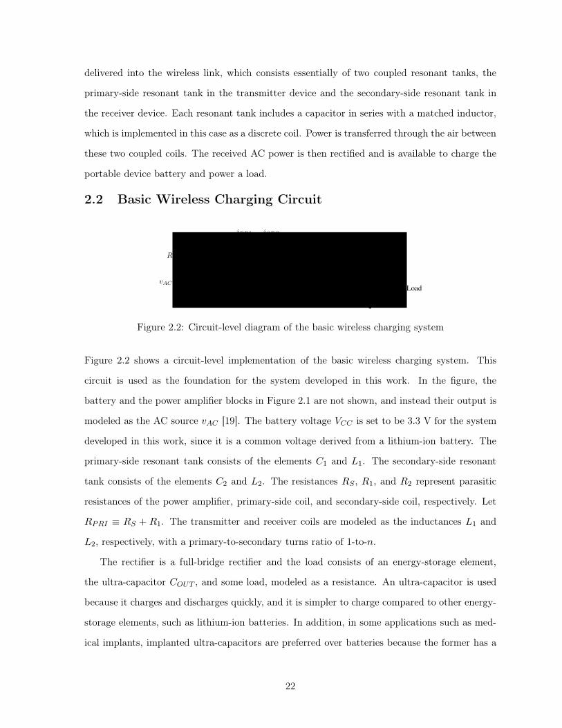
Figure 2.2: Circuit-level diagram of the basic wireless charging system
Figure 2.2 shows a circuit-level implementation of the basic wireless charging system. This
circuit is used as the foundation for the system developed in this work. In the figure, the
battery and the power amplifier blocks in Figure 2.1 are not shown, and instead their output is
modeled as the AC source vAC [19]. The battery voltage VCC is set to be 3.3 V for the system
developed in this work, since it is a common voltage derived from a lithium-ion battery. The
primary-side resonant tank consists of the elements C1 and L1. The secondary-side resonant
tank consists of the elements C2 and L2. The resistances RS , R1, and R2 represent parasitic
resistances of the power amplifier, primary-side coil, and secondary-side coil, respectively. Let
RPRI ≡ RS + R1. The transmitter and receiver coils are modeled as the inductances L1 and
L2, respectively, with a primary-to-secondary turns ratio of 1-to-n.
The rectifier is a full-bridge rectifier and the load consists of an energy-storage element,
the ultra-capacitor COUT , and some load, modeled as a resistance. An ultra-capacitor is used
because it charges and discharges quickly, and it is simpler to charge compared to other energy-
storage elements, such as lithium-ion batteries. In addition, in some applications such as med-
ical implants, implanted ultra-capacitors are preferred over batteries because the former has a
22
lifetime of many more charge cycles than the latter (millions to thousands) [20]. The ultra-
capacitor used in the system in this work is designed to be charged from a voltage of 2.5 V to
5 V.
A few other aspects of the basic wireless charging circuit are worth describing in more
detail in the following subsections, namely the operating frequency, the coil parameters, and
the coupling coefficient.
2.2.1 Operating Frequency
The operating frequency of the system developed in this work is 6.78 MHz. In other words,
the receiver resonant tank is tuned to resonate at 6.78 MHz, or 12π
√L2·C2
= 6.78 MHz. The
transmitter resonant tank is tuned to a slightly different frequency, the details of which are
described later. 6.78 MHz is chosen because it is an ISM band, an unregulated frequency spec-
trum range between 6.765 MHz and 6.795 MHz. The Federal Communications Commission
permits equipment used for “industrial, scientific, medical, domestic or similar purposes, ex-
cluding applications in the field of telecommunication” to transmit in this band with unlimited
energy [21]. Other ISM bands exist, such as at 13.56 MHz and 5.8 GHz. Poon et al. show that
operating in the gigahertz frequency range leads to lower dispersion in materials such as tissue
[22]. Using a higher operating frequency allows the coils to be made smaller, but also results in
higher losses in and more difficult design of the power amplifier. The 6.78 MHz band is chosen
as an acceptable tradeoff for this work, but the techniques developed can be applied to other
operating frequencies as well.
2.2.2 Coil Sizes and Inductances
The transmitter and receiver coils of the system developed in this work are sized after a common
wireless power application: a cochlear implant. In a conventional cochlear implant, the receiver
coil is about 25 mm in diameter [23]. Thus, the receiver coil in this system is designed to be
25 mm and the transmitter coil is designed to be slightly larger, 30 mm, for better coupling
with the receiver coil. At these dimensions, both coils are designed to have 5 uH inductance,
or L1 = L2 = 5 uH.
23

2.2.3 Coupling Coefficient
The primary-side transmitter coil and the secondary-side receiver coil are separated by material
that is not magnetically ideal, so the coils are not ideally coupled. A widely known metric for
the coupling quality of the two coils is the coupling coefficient k ≡ M√L1L2
, where M is the
mutual inductance. The mutual inductance between two one-turn coils is
Mi,j =2µ
α
√ri · rj
[(
1− α2
2
)
K(α)− E(α)
]
(2.2.1)
α = 2
√
ri · rj(ri + rj)2 + d2ij
(2.2.2)
where ri and rj are the radii of the two turns, µ is the permeability of the medium, dij is the
separation, and K(α) and E(α) are the complete elliptic integrals of the first and second kind,
respectively [24]. To find the total mutual inductance between two multi-turn coils, pairwise
sum the individual mutual inductances between each turn of the first coil and each turn of the
second coil, or M =∑
Mi,j.
4 6 8 10 12 14 16 18 200
0.05
0.1
0.15
0.2
0.25
0.3
0.35
0.4
0.45
0.5
Separation [mm]
Cou
plin
g C
oeffi
cien
t k
Coupling Coefficient vs. Separation for 30 mm / 25 mm Diameter Coils
Figure 2.3: Coupling coefficient variation with separation for 30 mm / 25 mm coils
Figure 2.3 shows the coupling coefficient change with separation between an 11.5-turn 30
mm diameter coil and a 17-turn 25 mm diameter coil, both with 5 uH inductances, based on
24

Equation 2.2.1.
2.3 Basic Wireless Charging Circuit Performance
This section analyzes the performance of the basic wireless charging circuit with respect to the
key user metrics of power and efficiency. To do this, a simplified equivalent circuit is derived
and analyzed.
2.3.1 Rectifier Equivalent Resistance
The impedance looking into the full-wave rectifier of Figure 2.2 from the left can be modeled
as a real resistance from the perspective of power transfer. As shown in [25], this resistance has
value
RL =4πVOUT
ISEC(2.3.1)
−vAC
+
PA Output
RS
R1 C1
iPRI
L1 L2
k:n
iSEC
C2R2
RL
Figure 2.4: Basic wireless charging circuit with equivalent output resistance
Figure 2.4 shows the wireless charging circuit with equivalent output resistance.
2.3.2 Primary-Side Equivalent Resistance
At resonance, real impedances can be reflected from the secondary side to the primary side.
Given that L2 and C2 are tuned to resonate at the operating frequency, in other words, given
that w = 1√L2C2
, then at resonance, the imaginary impedances on the secondary side cancel
out, and thus R2 + RL is the pure resistance looking into the secondary side. Reflecting this
25

back to the primary side, the resistance becomes
REQ =
(
k
n
)2
Q2L(RL +R2) =
k2L1
C2(RL +R2)=
(
k2L1
C2R2
)
‖(
k2L1
C2RL
)
(2.3.2)
This is the same result as derived in [19] using a transformer model. On the primary side at
resonance, the impedances of C1 and L1 may not entirely cancel, and there may be some excess
capacitance or inductance. Thus, the voltage across the primary side resonant tank may lead or
lag the current through it. However, a sinusoidal component vS of the power amplifier output
vAC is at the resonant frequency and in phase with the primary-side current. This is the only
component that can deliver power to REQ and thus the output.
2.3.3 Delivered Power
−vS
+
RS R1
REQ
+vEQ
−
Figure 2.5: Primary-side equivalent circuit for power transfer
Figure 2.5 shows the equivalent circuit for the basic wireless charging circuit, keeping only the
component of the circuit that transfers power to the output. From [19], the average output
power is
POUT = V 2S,rms
(
k2L1C2RL
(k2L1 + C2RPRI(RL +R2))2
)
(2.3.3)
2.3.4 Efficiency
Figures 2.4 and 2.5 can be used to calculate the power efficiency of the basic wireless charging
circuit. This ignores the efficiency of the power amplifier and full-wave rectifier, both important
contributions that are considered later. The efficiency is simply the product of the primary and
secondary efficiencies, or
η =
(
REQ
REQ +RPRI
)
×(
RL
RL +R2
)
(2.3.4)
26
2.4 Basic Power Amplifier Circuit
The power amplifier converts the DC energy from the transmitter’s battery to AC energy to
drive the transmitter coil. A Class-E power amplifier is selected for the system in this work
because of its high efficiency, ideally 100%.
−VCC
+
LCHOKE
IO
v(wt)
iS
q(t)
iC
CP
iR
CR
LR
LEX
+
vEX(wt)
−
RPRI +REQ
+
vS(wt)
−
Figure 2.6: Basic Class-E power amplifier circuit
Figure 2.6 shows a basic Class-E power amplifier circuit. The PA draws DC current from the
battery VCC and converts it to AC current through the resonant tank created by the capacitance
CR and inductance LR + LEX .
Figure 2.7: Class-E power amplifier waveforms
Figure 2.7 shows waveforms of the switch drive voltage (blue trace v_gate), the switch
drain voltage v(wt) (green trace v_switch), and the resonant tank current (red trace L1).
The switch drain voltage reaches zero just as the switch turns on, satisfying the zero-voltage
switching (ZVS) condition that gives the power amplifier perfect ideal efficiency. The switch
drain voltage also leads the resonant tank current. This is caused by the excess inductance LEX
(CR and LR resonate at the operating frequency of the power amplifier, or 12π
√LRCR
= 6.78
MHz). Only with this excess inductance can ZVS be achieved.
27

In relation to the basic wireless charging circuit of Figure 2.2, vAC = v(wt), C1 = CR,
L1 = LR + LEX , R1 +RS = RPRI , and REQ is the reflected load impedance at resonance. At
the operating frequency, the imaginary impedances of CR and LR cancel but the impedance of
LEX remains. Thus, a portion (vS in Figures 2.5 and 2.6) of v(wt) at the fundamental frequency
and in phase with iR is dropped across the resonant tank resistance and a portion out of phase
is dropped across the excess inductance.
2.5 Chapter Summary
This chapter analyzes the operation of the basic wireless power circuit with respect to the key
metrics of efficiency and power. The mathematical analysis in the following chapters shows the
performance of previously published systems based on this circuit and derives improvements to
this basic topology.
Parameter Value
Battery Voltage 3.3 V
Operating Frequency 6.78 MHz
Primary-Side Coil 5 uH, 30 mm diameter
Secondary-Side Coil 5 uH, 25 mm diameter
Power Amplifier Class-E
Rectifier Full-wave discrete rectifier
Output Ultra-capacitor (2.5 V - 5 V)
Table 2.1: Summary of basic parameters used in this work
Table 2.1 shows a summary of the basic parameters used for the system developed in this
work.
28

Chapter 3
Design Overview and Previous Work
3.1 Wireless Charging System Design Overview
In light of the portable-to-portable wireless charging use cases presented in Chapter 1, some
critical design challenges must be addressed by the wireless charging system in this work. Design
objectives are derived to meet these challenges, and an overall system design that satisfies these
objectives is presented.
3.1.1 Design Challenges
The portable-to-portable wireless charging application presents a number of obstacles to achiev-
ing good performance along the key user metrics of high efficiency and consistent delivered
power. These obstacles come from the fact that both the transmitter and receiver in this ap-
plication are portable, so the charging environment is highly dynamic. In contrast, the wireless
power applications most consumer systems are designed for are relatively static, such as charg-
ing a cell phone sitting on a charging pad. In this more static case, the associated wireless
power systems can be optimized around a more constant condition.
On the other hand, the transmitter-receiver coupling in a portable-to-portable charging
application may vary dramatically, since both devices may move with respect to each other. In
addition, the receiver is a low-power device and charges quickly (in a couple minutes), so the
output loading changes quickly as well. In the case of the system developed in this work, the
receiver charges an ultra-capacitor at the output, and the load voltage of this ultra-capacitor
29

changes relatively quickly.
All of these changing conditions have a significant effect on the end-to-end efficiency and
delivered power. Thus, the main design challenge is to achieve high efficiency and balanced
delivered power across these changing coupling and load conditions.
3.1.2 Design Objectives
The wireless charging system developed in this work meets the design challenge described in
the preceding subsection. There are three general objectives for the system developed in this
work:
1. Rapidly recharge a receiver portable device in about two minutes. This enables
quickly recharging a portable device on the go, which is convenient for the user. The
average delivered power specification is derived from being able to charge an MP3 player
in two minutes, which is one of the representative use cases highlighted in Chapter 1. From
measurements of an iPod Shuffle, a common MP3 player, it draws about 13 mW of power
during operation. From the use case, this device should be able to be recharged in two
minutes to last 30 minutes. Thus, the required average delivered power is 13× 302 ≈ 200
mW.
2. High end-to-end charging efficiency. This minimizes the battery drain of the trans-
mitting mobile device, which is important for the user since mobile device battery life is
valuable. The target peak end-to-end efficiency for this system is 75%.
3. Maintain high efficiency and balanced power levels with changing conditions.
This system must maintain high efficiency and about 200 mW delivered power levels
across the range of coupling and load conditions that the portable-to-portable application
may entail. For the cochlear implant and MP3 player recharging use cases described
in Chapter 1, typical separation distances may be 7-12 mm. Over these distances and
averaged over the full charging range, the end-to-end efficiency should be greater than
70%. The delivered power has a relatively small impact on a short charging time, so
30
it can be allowed to vary slightly. The delivered power level should stay within a 40%
variation across operating conditions, which is typical of previous work [3].
Design Objective Target
Nominal Delivered Power 200 mW
Peak Efficiency 75%
Operating Separation Distances 7-12 mm
Efficiency, Power over Distance/Load > 70%, < 40% variation
Table 3.1: Design objectives for wireless charging system in this work
Table 3.1 summarizes the design objectives for this work.
3.1.3 Design Overview
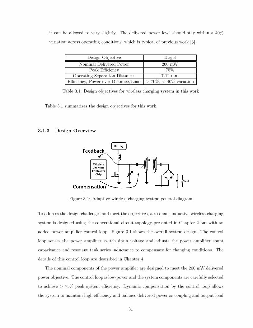
Figure 3.1: Adaptive wireless charging system general diagram
To address the design challenges and meet the objectives, a resonant inductive wireless charging
system is designed using the conventional circuit topology presented in Chapter 2 but with an
added power amplifier control loop. Figure 3.1 shows the overall system design. The control
loop senses the power amplifier switch drain voltage and adjusts the power amplifier shunt
capacitance and resonant tank series inductance to compensate for changing conditions. The
details of this control loop are described in Chapter 4.
The nominal components of the power amplifier are designed to meet the 200 mW delivered
power objective. The control loop is low-power and the system components are carefully selected
to achieve > 75% peak system efficiency. Dynamic compensation by the control loop allows
the system to maintain high efficiency and balance delivered power as coupling and output load
31

conditions change. This control loop approach is compared to previous work in the next section.
3.2 Previous Implementations of Wireless Power Systems
Many researchers have developed wireless power systems at similar power levels and with similar
dimensions as those of interest. Each system is analyzed with respect to the user metrics of
end-to-end efficiency at a desired delivered power level. Four implementations are considered,
each with a different approach to handling changing coupling and load conditions. The first
work implements no dynamic control, the second work implements power amplifier sensing and
a set delay, the third work implements dynamic power amplifier duty cycle control, and the
fourth work implements dynamic power amplifier supply voltage control.
3.2.1 Lo et al., IEEE Biomedical Circuits and Systems 2013 [1]
This previous work describes the design of an epi-retinal and neural prostheses SoC incorporat-
ing wireless power transfer. Due to the many electrodes required to stimulate retinal neurons
for acceptable granularity, this system requires relatively high constant power, about 100 mW.
A circuit is designed to transmit this power from a 39 mm diameter transmitter coil to a 19 mm
diameter receiver coil, separated by distances of 1-3 cm. A standard Class-E power amplifier
is used in the transmitter at an operating frequency of 2 MHz. The outputs are fixed ±2V
and ±12V supplies generated with CMOS rectifiers and on-chip regulators for constant power
delivery to the load.
With this system design, the end-to-end efficiency is 24% at 10 mm coil separation, and
the rectifier efficiency is 72%. In addition, the end-to-end efficiency increases to a peak of 40%
at 17 mm separation before declining to 15% at 30 mm separation. The supply voltage of the
transmitter power amplifier is manually adjusted to regulate the delivered power for each coil
separation. This thesis differs from the previous work in that this thesis presents a dynamic
power amplifier control circuit that achieves higher efficiency and automatically controls power
levels over changing conditions.
32
3.2.2 Kendir et al., IEEE Circuits and Systems 2005 [2]
This previous work describes an efficiency-based design methodology for the components in
a wireless power system. The system transfers 250 mW of power from a 36 mm diameter
transmit coil to a 20 mm diameter receive coil, separated by 2-15 mm. A standard Class-E
power amplifier is used in the transmitter at an operating frequency of 1 MHz. The output
is a fixed 16 V supply generated with a discrete half-wave rectifier. The authors derive an
optimal coil design considering the coil losses. In addition, the work proposes calculating the
time delay between the point at which the resonant tank current reaches zero and when the
power amplifier switch drain voltage reaches zero, sensing the zero-crossing point of the resonant
tank current, and waiting that precise amount of time to turn on the switch for zero-voltage
switching. Switching the power amplifier at zero voltage increases the system efficiency. The
wireless power system implements this precise time delay calculated at a single coil separation
of 7 mm.
The efficiency of the reported system is 65% at 2 mm separation, 67% at 7 mm separation,
and 51% at 15 mm separation. The efficiency is optimized at the single separation of 7 mm, while
zero-voltage switching is not satisfied at other separations. In this previous work the delivered
power is kept constant across different separations by manual adjustment of the transmitter
power amplifier supply voltage. This thesis differs from the previous work in that this thesis
presents a lower power dynamic power amplifier control circuit that automatically maintains
optimal efficiency and balanced power for a range of separations.
3.2.3 Baker, Sarpeshkar, IEEE Biomedical Circuits and Systems 2007 [3]
This previous work investigates feedback circuits in wireless power systems for bionic devices.
The power circuits are designed to deliver up to 10 mW of power through 30 mm diameter
transmitter and receiver coils separated by 1-10 mm. The output is a fixed 3.4 V supply
generated with a discrete half-wave rectifier. The paper presents an enhanced Class-E power
amplifier operating at 6.78 MHz. The PA incorporates a feedback circuit that detects when
the switch drain voltage has reached zero to attempt to always turn on the MOSFET under
zero-voltage switching conditions, which increases system efficiency. The feedback adjusts the
33
duty cycle and frequency of operation so zero-voltage switching can be achieved.
With this configuration, the system achieves end-to-end efficiency of 54% at 10 mm sepa-
ration and 60% at 7 mm separation. The rectifier efficiency is 96%. At a transmitter power
amplifier supply voltage of 2.35 V, the output voltage varies from 5.9 V at 5 mm separation to 5
V at 10 mm separation, so the delivered power varies by 5.92−52
52= 39%. This thesis differs from
the previous work in that this thesis presents a feedback circuit for the power amplifier based
on adjusting the power amplifier component values instead of adjusting its switching duty cycle
and frequency. The fixed frequency and fixed 50% duty cycle of the power amplifier in this
thesis limits undesired out-of-band or harmonic energy. Adjusting the power amplifier compo-
nent values also allows the power amplifier to have zero-voltage switching in a wider range of
cases, especially when the switch drain voltage tends to be positive at switch turn-on. Also,
adjusting the power amplifier component values keeps the delivered power consistent across
changing conditions in addition to optimizing the system efficiency.
3.2.4 Wang et al., IEEE Circuits and Systems 2005 [4]
This previous work develops a wireless power system delivering 250 mW to a retinal implant.
The authors use a 40 mm diameter transmitter coil and a 22 mm diameter receive coil. The
transmitter includes a Class-E power amplifier operating at 1 MHz. The output is a fixed 15 V
supply generated with a discrete half-wave rectifier and linear regulator circuits. The wireless
power system incorporates a feedback circuit that determines the output power and commu-
nicates this information back through the power link using a load-shift keying technique. The
transmitter circuit then adjusts the power amplifier supply voltage to regulate the transmitted
power, so that the output voltage stays around 15 V.
With this design, the system achieves end-to-end efficiency of 65.8% at 7 mm separation
and 36.3% at 15 mm separation. This thesis differs from the previous work in that this thesis
presents a control loop that not only regulates power but also optimizes efficiency over changing
conditions.
34

3.3 Chapter Summary
Work Approach Power Peak Eff. Off-Peak Eff.
ObjectiveDynamic PA
capacitance / inductance200 mW > 75% > 70% 7-12 mm
Lo et al. No dynamic control 100 mW 40% 24% 10 mm
Kendir et al.Resonant current
zero-crossing detect250 mW 67%
65% 2 mm,51% 15 mm
BakerDynamic PA
duty cycle / frequency10 mW 60% 54% 10 mm
Wang et al. Dynamic PA supply voltage 250 mW 65.8% 36.3% 15 mm
Table 3.2: Comparison of this system design approach to previous approaches
Table 3.2 shows a summary comparing the approach of this work to previous work. The
unique control loop proposed allows the system to achieve higher peak efficiencies and higher
efficiencies over changing separation distances while delivering consistent power levels. The next
chapter presents the mathematical analysis detailing the proposed control loop.
35
Chapter 4
Power Amplifier Control Loop for High
Efficiency and Balanced Power
This chapter details the power amplifier control loop described in Chapter 3 for increasing
system efficiency and balancing delivered power across changing conditions. A block-level effi-
ciency analysis is first performed to show that power amplifier and wireless link block efficiency
is important. This block is then analyzed to show that power amplifier zero-voltage switching
optimizes its efficiency. Finally, a method is derived for dynamically tuning the power ampli-
fier to maintain zero-voltage switching while balancing power across changing conditions. The
power amplifier control loop adopts this feedback and compensation method.
4.1 Block-Level Efficiency Breakdown
Efficiency of the system at the block-level as illustrated in Figure 2.1 is determined through
SPICE simulation. The combined transmitter and receiver system is broken into two major
blocks: the power amplifier and wireless link block and the rectifier block. The system is
separated this way because these two blocks are generally decoupled from each other.
36
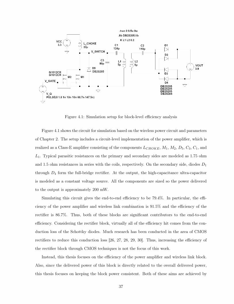
Figure 4.1: Simulation setup for block-level efficiency analysis
Figure 4.1 shows the circuit for simulation based on the wireless power circuit and parameters
of Chapter 2. The setup includes a circuit-level implementation of the power amplifier, which is
realized as a Class-E amplifier consisting of the components LCHOKE, M1, M2, D5, C3, C1, and
L1. Typical parasitic resistances on the primary and secondary sides are modeled as 1.75 ohm
and 1.5 ohm resistances in series with the coils, respectively. On the secondary side, diodes D1
through D4 form the full-bridge rectifier. At the output, the high-capacitance ultra-capacitor
is modeled as a constant voltage source. All the components are sized so the power delivered
to the output is approximately 200 mW.
Simulating this circuit gives the end-to-end efficiency to be 79.4%. In particular, the effi-
ciency of the power amplifier and wireless link combination is 91.5% and the efficiency of the
rectifier is 86.7%. Thus, both of these blocks are significant contributors to the end-to-end
efficiency. Considering the rectifier block, virtually all of the efficiency hit comes from the con-
duction loss of the Schottky diodes. Much research has been conducted in the area of CMOS
rectifiers to reduce this conduction loss [26, 27, 28, 29, 30]. Thus, increasing the efficiency of
the rectifier block through CMOS techniques is not the focus of this work.
Instead, this thesis focuses on the efficiency of the power amplifier and wireless link block.
Also, since the delivered power of this block is directly related to the overall delivered power,
this thesis focuses on keeping the block power consistent. Both of these aims are achieved by
37

dynamically tuning the power amplifier and wireless link, which is analyzed in further detail
next.
4.2 Power Amplifier and Wireless Link Analysis Strategy
The goal of the following analysis is to identify and optimize the factors that determine effi-
ciency and delivered power of the power amplifier and wireless link block under changing load
and coupling conditions. This is done in a few steps. First, zero-voltage switching (ZVS) is the-
oretically shown to be the optimal efficiency condition. Next, the effect of changing conditions
on the primary-side equivalent resistance is analyzed. This is used to show the effect of chang-
ing equivalent resistance on power amplifier ZVS. Two types of ZVS are analyzed: full ZVS, in
which the power amplifier switch drain voltage and slope are both zero at switch turn-on, and
general ZVS, in which just the voltage is zero. In either case, ZVS can be maintained across
changing conditions by dynamically tuning the power amplifier shunt capacitance and reso-
nant tank inductance. Maintaining the full ZVS condition increases efficiency, but maintaining
the general ZVS condition provides the flexibility to balance the delivered power at the same
time. This analysis is used to derive a method to compensate the power amplifier capacitance
and inductance that maintains high block efficiency while also balancing delivered power under
changing conditions. Simulation results at the end of this chapter support the mathematical
analysis.
4.3 Effect of Power Amplifier Zero-Voltage Switching on Effi-
ciency
In general, the power amplifier drain voltage waveform v(wt) can be in one of three cases, as
shown in Figure 4.2.
38
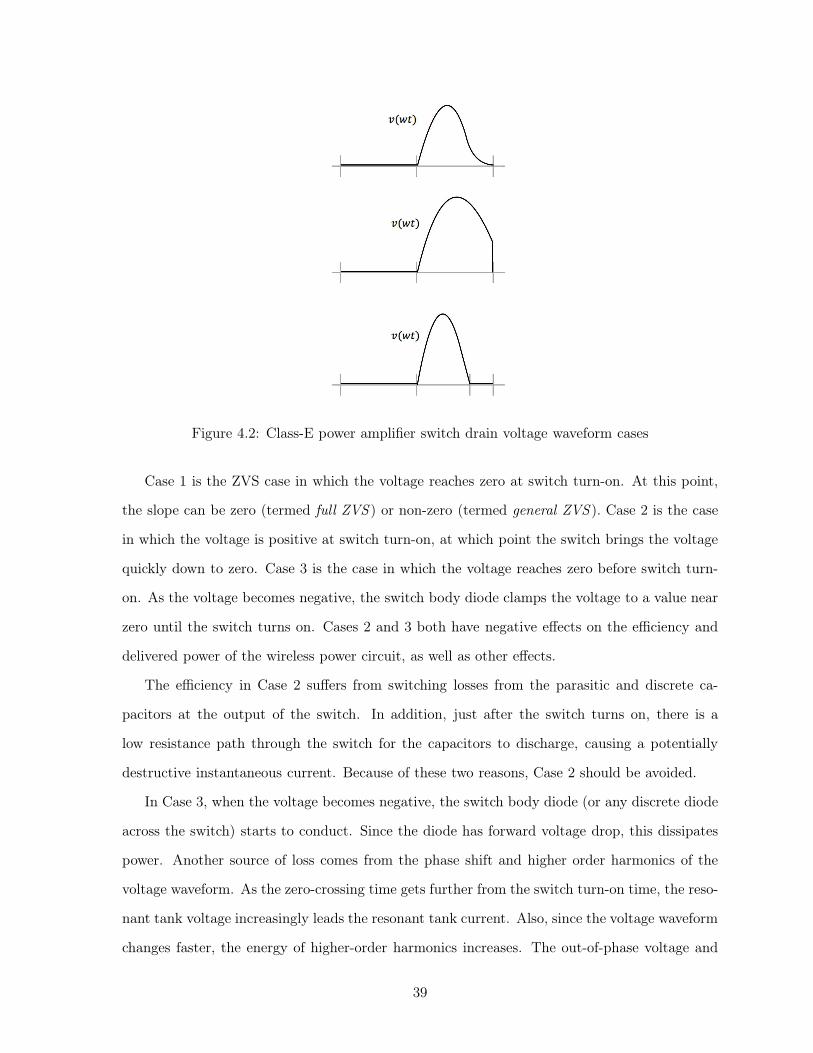
Figure 4.2: Class-E power amplifier switch drain voltage waveform cases
Case 1 is the ZVS case in which the voltage reaches zero at switch turn-on. At this point,
the slope can be zero (termed full ZVS ) or non-zero (termed general ZVS ). Case 2 is the case
in which the voltage is positive at switch turn-on, at which point the switch brings the voltage
quickly down to zero. Case 3 is the case in which the voltage reaches zero before switch turn-
on. As the voltage becomes negative, the switch body diode clamps the voltage to a value near
zero until the switch turns on. Cases 2 and 3 both have negative effects on the efficiency and
delivered power of the wireless power circuit, as well as other effects.
The efficiency in Case 2 suffers from switching losses from the parasitic and discrete ca-
pacitors at the output of the switch. In addition, just after the switch turns on, there is a
low resistance path through the switch for the capacitors to discharge, causing a potentially
destructive instantaneous current. Because of these two reasons, Case 2 should be avoided.
In Case 3, when the voltage becomes negative, the switch body diode (or any discrete diode
across the switch) starts to conduct. Since the diode has forward voltage drop, this dissipates
power. Another source of loss comes from the phase shift and higher order harmonics of the
voltage waveform. As the zero-crossing time gets further from the switch turn-on time, the reso-
nant tank voltage increasingly leads the resonant tank current. Also, since the voltage waveform
changes faster, the energy of higher-order harmonics increases. The out-of-phase voltage and
39
higher-order harmonics both do not deliver power to the load. Another interpretation of this
situation is that the power factor of the power amplifier is increasingly lower than one. Thus,
in order to keep the same delivered power, the input power must be increased, which causes
more losses due to the parasitic resistances of the power amplifier (such as the resistances of the
choke inductor and power switch). Hence, keeping the same delivered power is at the cost of
decreased efficiency, or keeping the same efficiency is at the cost of decreased delivered power.
Both of these situations are undesirable. In addition, since the voltage is positive for a shorter
time, the peak of the voltage waveform is higher. This is because since the average voltage
across the choke inductor is zero, the average of the switch voltage is always equal to the DC
voltage VCC . This higher peak causes greater stress on the power switch, and to accommodate
this higher stress a power switch might have to be chosen that has more parasitics than a switch
that can tolerate lower stresses. For all of these reasons, Case 3 should be avoided.
In summary, the power amplifier and wireless link block achieves maximum efficiency across
conditions when ZVS is maintained. Note that even when ZVS is maintained, delivered power
can still vary with changing conditions, so the system must not only maintain ZVS but also
regulate power. The following analysis shows how ZVS is affected by changing conditions and
shows how to maintain ZVS in these situations.
4.4 Effect of Changing Conditions on Equivalent Resistance
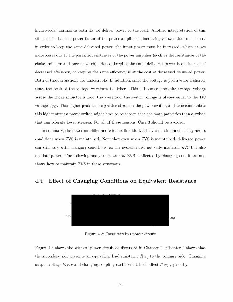
−vAC
+
PA Output
RS
R1 C1
iPRI
L1 L2
k:n
iSEC
C2R2
iOUT
COUT
+vOUT− Load
Figure 4.3: Basic wireless power circuit
Figure 4.3 shows the wireless power circuit as discussed in Chapter 2. Chapter 2 shows that
the secondary side presents an equivalent load resistance REQ to the primary side. Changing
output voltage VOUT and changing coupling coefficient k both affect REQ , given by
40
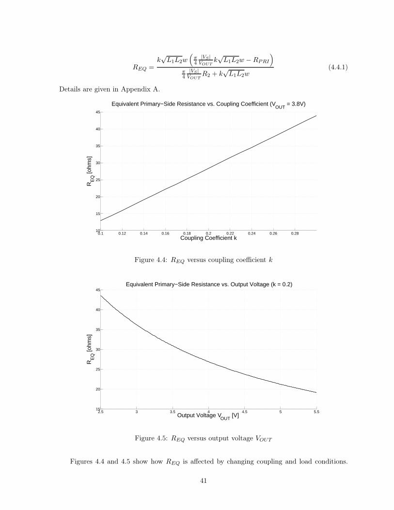
REQ =k√L1L2w
(
π4
|VS |VOUT
k√L1L2w −RPRI
)
π4
|VS |VOUT
R2 + k√L1L2w
(4.4.1)
Details are given in Appendix A.
0.1 0.12 0.14 0.16 0.18 0.2 0.22 0.24 0.26 0.2810
15
20
25
30
35
40
45
Coupling Coefficient k
RE
Q [o
hms]
Equivalent Primary−Side Resistance vs. Coupling Coefficient (VOUT
= 3.8V)
Figure 4.4: REQ versus coupling coefficient k
2.5 3 3.5 4 4.5 5 5.515
20
25
30
35
40
45
Output Voltage VOUT
[V]
RE
Q [o
hms]
Equivalent Primary−Side Resistance vs. Output Voltage (k = 0.2)
Figure 4.5: REQ versus output voltage VOUT
Figures 4.4 and 4.5 show how REQ is affected by changing coupling and load conditions.
41
Intuitively, increasing the coupling coefficient or decreasing the output voltage should increase
the loading on the primary side, hence the higher REQ.
4.5 Maintaining Power Amplifier Full ZVS
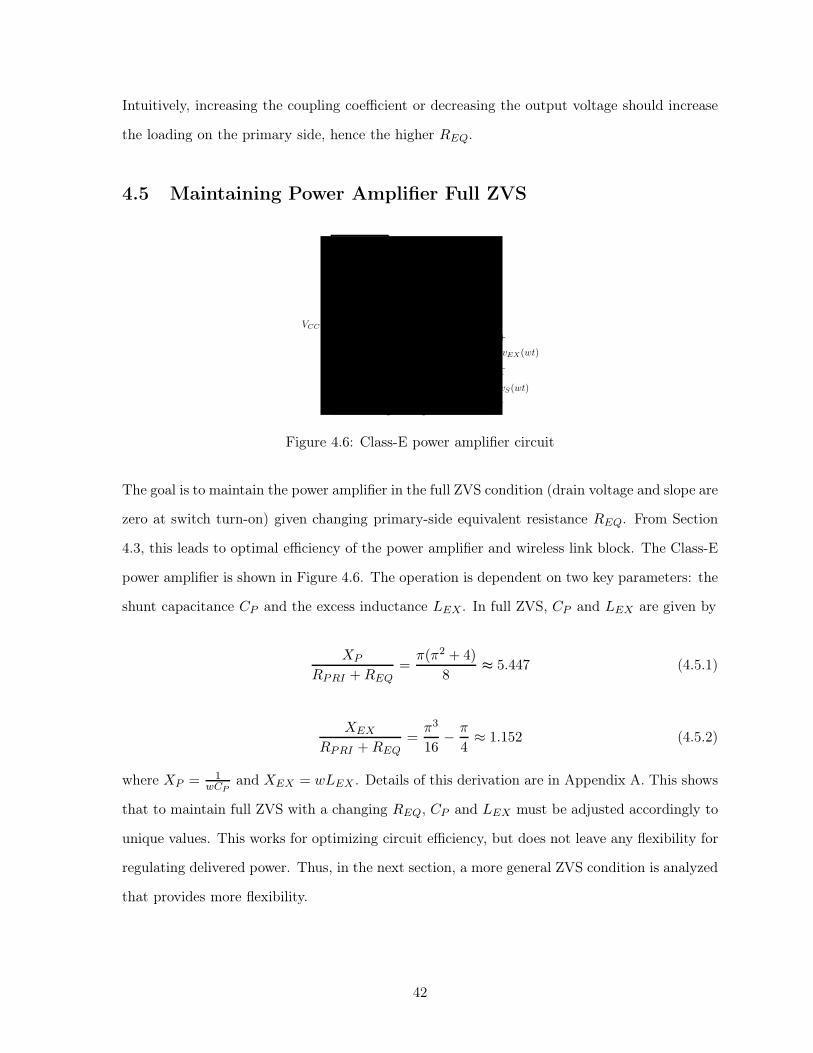
−VCC
+
LCHOKE
IO
v(wt)
iS
q(t)
iC
CP
iR
CR
LR
LEX
+
vEX(wt)
−
RPRI +REQ
+
vS(wt)
−
Figure 4.6: Class-E power amplifier circuit
The goal is to maintain the power amplifier in the full ZVS condition (drain voltage and slope are
zero at switch turn-on) given changing primary-side equivalent resistance REQ. From Section
4.3, this leads to optimal efficiency of the power amplifier and wireless link block. The Class-E
power amplifier is shown in Figure 4.6. The operation is dependent on two key parameters: the
shunt capacitance CP and the excess inductance LEX . In full ZVS, CP and LEX are given by
XP
RPRI +REQ=
π(π2 + 4)
8≈ 5.447 (4.5.1)
XEX
RPRI +REQ
=π3
16− π
4≈ 1.152 (4.5.2)
where XP = 1wCP
and XEX = wLEX . Details of this derivation are in Appendix A. This shows
that to maintain full ZVS with a changing REQ, CP and LEX must be adjusted accordingly to
unique values. This works for optimizing circuit efficiency, but does not leave any flexibility for
regulating delivered power. Thus, in the next section, a more general ZVS condition is analyzed
that provides more flexibility.
42
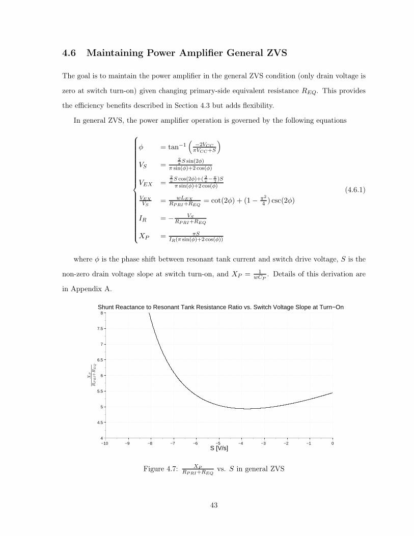
4.6 Maintaining Power Amplifier General ZVS
The goal is to maintain the power amplifier in the general ZVS condition (only drain voltage is
zero at switch turn-on) given changing primary-side equivalent resistance REQ. This provides
the efficiency benefits described in Section 4.3 but adds flexibility.
In general ZVS, the power amplifier operation is governed by the following equations
φ = tan−1(
−2VCC
πVCC+S
)
VS =2
πS sin(2φ)
π sin(φ)+2 cos(φ)
VEX =2
πS cos(2φ)+( 2
π−π
2)S
π sin(φ)+2 cos(φ)
VEX
VS= wLEX
RPRI+REQ= cot(2φ) + (1− π2
4 ) csc(2φ)
IR = − VS
RPRI+REQ
XP = πSIR(π sin(φ)+2 cos(φ))
(4.6.1)
where φ is the phase shift between resonant tank current and switch drive voltage, S is the
non-zero drain voltage slope at switch turn-on, and XP = 1wCP
. Details of this derivation are
in Appendix A.
−10 −9 −8 −7 −6 −5 −4 −3 −2 −1 04
4.5
5
5.5
6
6.5
7
7.5
8
S [V/s]
XP
RPRI+
REQ
Shunt Reactance to Resonant Tank Resistance Ratio vs. Switch Voltage Slope at Turn−On
Figure 4.7: XP
RPRI+REQvs. S in general ZVS
43
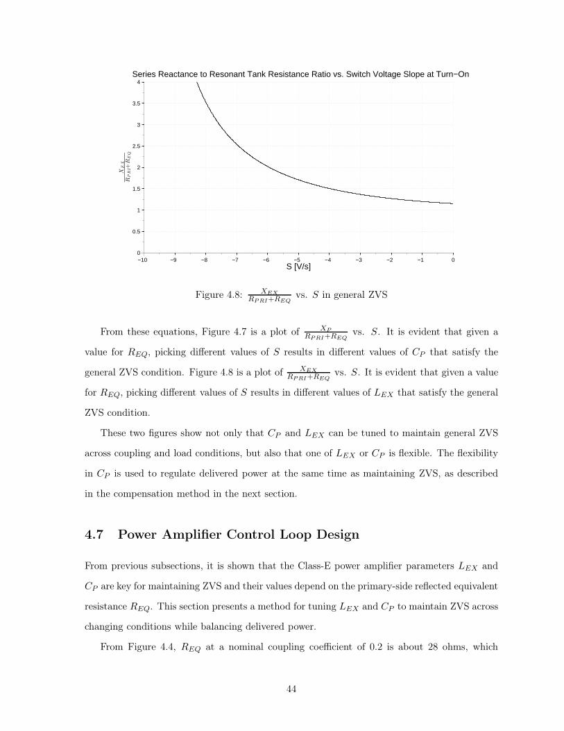
−10 −9 −8 −7 −6 −5 −4 −3 −2 −1 00
0.5
1
1.5
2
2.5
3
3.5
4
S [V/s]
XEX
RPRI+
REQ
Series Reactance to Resonant Tank Resistance Ratio vs. Switch Voltage Slope at Turn−On
Figure 4.8: XEX
RPRI+REQvs. S in general ZVS
From these equations, Figure 4.7 is a plot of XP
RPRI+REQvs. S. It is evident that given a
value for REQ, picking different values of S results in different values of CP that satisfy the
general ZVS condition. Figure 4.8 is a plot of XEX
RPRI+REQvs. S. It is evident that given a value
for REQ, picking different values of S results in different values of LEX that satisfy the general
ZVS condition.
These two figures show not only that CP and LEX can be tuned to maintain general ZVS
across coupling and load conditions, but also that one of LEX or CP is flexible. The flexibility
in CP is used to regulate delivered power at the same time as maintaining ZVS, as described
in the compensation method in the next section.
4.7 Power Amplifier Control Loop Design
From previous subsections, it is shown that the Class-E power amplifier parameters LEX and
CP are key for maintaining ZVS and their values depend on the primary-side reflected equivalent
resistance REQ. This section presents a method for tuning LEX and CP to maintain ZVS across
changing conditions while balancing delivered power.
From Figure 4.4, REQ at a nominal coupling coefficient of 0.2 is about 28 ohms, which
44

corresponds to a nominal LEX of 0.8 µH according to Equation 4.5.2. When REQ changes due
to changing coupling or load, LEX must adjust as well. The tuning range of LEX determines
the range of REQ and thus the range of conditions that the system can handle while maintaining
zero drain voltage at switch turn-on. In this work, LEX is chosen to be tunable from 0.7 uH to
0.9 uH. For full ZVS, this corresponds to a range of REQ between 24 ohms and 32 ohms. From
Figure 4.4, for a nominal output load of VOUT = 3.8 V, this corresponds to a coupling coefficient
range between 0.175 and 0.22. From Figure 2.3, ZVS is maintained for a coil separation range
between about 8 mm and about 10 mm. From Figure 4.5, for a nominal coupling coefficient of
k = 0.2, ZVS is maintained for an output voltage range between 3.4 V and 4.5 V.
From the analysis in Section 4.5 of full ZVS, the tuning range of LEX uniquely determines
the tuning range of CP . While full ZVS optimizes efficiency, the delivered power can vary
greatly with changing conditions.
45
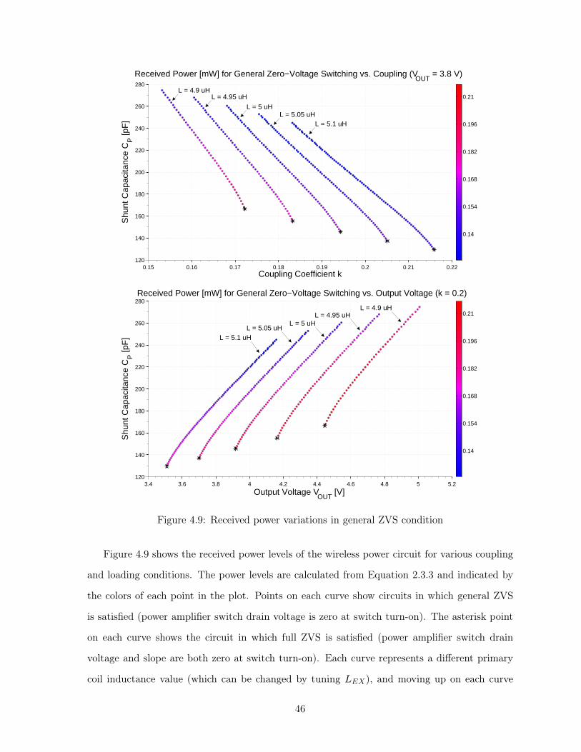
0.15 0.16 0.17 0.18 0.19 0.2 0.21 0.22120
140
160
180
200
220
240
260
280
Coupling Coefficient k
Shu
nt C
apac
itanc
e C
P [p
F]
Received Power [mW] for General Zero−Voltage Switching vs. Coupling (VOUT
= 3.8 V)
0.14
0.154
0.168
0.182
0.196
0.21L = 4.9 uH
L = 4.95 uH
L = 5 uHL = 5.05 uH
L = 5.1 uH
3.4 3.6 3.8 4 4.2 4.4 4.6 4.8 5 5.2120
140
160
180
200
220
240
260
280
Output Voltage VOUT
[V]
Shu
nt C
apac
itanc
e C
P [p
F]
Received Power [mW] for General Zero−Voltage Switching vs. Output Voltage (k = 0.2)
0.14
0.154
0.168
0.182
0.196
0.21
L = 5.1 uHL = 5.05 uH
L = 5 uHL = 4.95 uH
L = 4.9 uH
Figure 4.9: Received power variations in general ZVS condition
Figure 4.9 shows the received power levels of the wireless power circuit for various coupling
and loading conditions. The power levels are calculated from Equation 2.3.3 and indicated by
the colors of each point in the plot. Points on each curve show circuits in which general ZVS
is satisfied (power amplifier switch drain voltage is zero at switch turn-on). The asterisk point
on each curve shows the circuit in which full ZVS is satisfied (power amplifier switch drain
voltage and slope are both zero at switch turn-on). Each curve represents a different primary
coil inductance value (which can be changed by tuning LEX), and moving up on each curve
46

represents increasing the shunt capacitance CP .
This figure shows that if the wireless power system attempts to maintain full ZVS, then
as the coupling coefficient decreases or as load voltage increases, the received power increases
dramatically. Thus, it is necessary to relax the conditions on the system and instead attempt to
maintain general ZVS. This gives the added flexibility of being able to tune the shunt capacitance
CP to regulate delivered power without significant effect on efficiency [31]. In particular, if
CP is increased significantly as the coupling decreases or the load voltage increases, then the
delivered power increases less. This is intuitively apparent, because increasing CP decreases its
impedance, which shunts power away from the resonant tank.
In this work, a unique value of CP is chosen for each value of LEX such that as conditions
change within the ranges in Figure 4.9, general ZVS is maintained to increase efficiency and
balance power at the same time. Specifically, Table 4.1 shows five tunable settings adopted in
this work.
Compensation Setting Excess Inductance LEX Shunt Capacitance CP
D 0.7 uH 240 pF
C 0.75 uH 190 pF
B 0.8 uH 160 pF
A 0.85 uH 140 pF
Z 0.9 uH 130 pF
Table 4.1: Tunable excess inductance and shunt capacitance values used in design
The aim of this work is to design a closed-loop control system for the basic Class-E power
amplifier that senses the switch voltage at the turn-on time and determines if the power am-
plifier is in a ZVS condition. If not, the system adjusts the excess inductance LEX and shunt
capacitance CP to bring the power amplifier closer to ZVS while keeping the power consistent.
4.8 Meeting the Design Objectives
This section shows that the wireless power circuit with Class-E control designed in the previous
sections satisfies the design objectives presented in Chapter 3.
Combining the equations for efficiency and primary-side equivalent resistance from Subsec-
tion 2.3.4 and Section 4.4, the nominal efficiency of the power amplifier and wireless link block
47

is
η =
π4
|VS |VOUT
k√L1L2w −RPRI
π4
|VS |VOUT
k√L1L2w +
(
π4
|VS |VOUT
)2R2)
(4.8.1)
Using the basic parameters in Chapter 2 and Section 4.1, and the nominal values k = 0.2 and
VOUT = 3.8 V (typical for the wireless charging application), the nominal efficiency is η = 92.0%.
This value matches the simulation results of the same circuit in Section 4.1 very closely. A
typical rectifier efficiency is 90%, so the end-to-end efficiency is about 0.92 × 0.90 = 83%. The
Class-E control loop is low-power and does not significantly affect this efficiency. This meets
the design objective of 75%.
From Equation 2.3.3, the average received power is POUT = 189 mW. This power is delivered
to the rectifier, which has a typical efficiency of 90%, so the delivered power to the load is
nominally 189 × 0.9 = 170 mW. This is relatively close to the design objective of 200 mW.
The efficiency and power specifications over variations in coupling and load are shown to be
met in the simulation results in the next section.
4.9 Simulation Results
This section aims to show that the power amplifier control method derived in Section 4.7
indeed improves the efficiency and balances the delivered power of a wireless charging system
over changing conditions.
The simulation circuit is the same as the one used in Section 4.1. To implement the control
method of Section 4.7, the tunable parameters are the Class-E power amplifier resonant tank
inductance L1 (which includes LEX) and shunt capacitance CP (including the discrete capac-
itance C3 and about 100 pF of parasitic switch and diode output capacitance). The coupling
and load parameters that are changed are the coupling coefficient k and the output voltage
VOUT , respectively.
Two simulations are performed. First, simulations show that changing coupling and load
both affect the switch drain voltage at switch turn-on, and that compensating the power am-
plifier brings the power amplifier back towards the ZVS condition. One representative case is
shown, and other cases are presented in Appendix A. Second, simulations show that the control
48
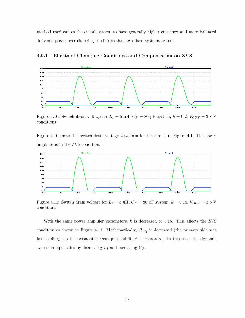
method used causes the overall system to have generally higher efficiency and more balanced
delivered power over changing conditions than two fixed systems tested.
4.9.1 Effects of Changing Conditions and Compensation on ZVS
Figure 4.10: Switch drain voltage for L1 = 5 uH, CP = 80 pF system, k = 0.2, VOUT = 3.8 Vconditions
Figure 4.10 shows the switch drain voltage waveform for the circuit in Figure 4.1. The power
amplifier is in the ZVS condition.
Figure 4.11: Switch drain voltage for L1 = 5 uH, CP = 80 pF system, k = 0.15, VOUT = 3.8 Vconditions
With the same power amplifier parameters, k is decreased to 0.15. This affects the ZVS
condition as shown in Figure 4.11. Mathematically, REQ is decreased (the primary side sees
less loading), so the resonant current phase shift |φ| is increased. In this case, the dynamic
system compensates by decreasing L1 and increasing CP .
49
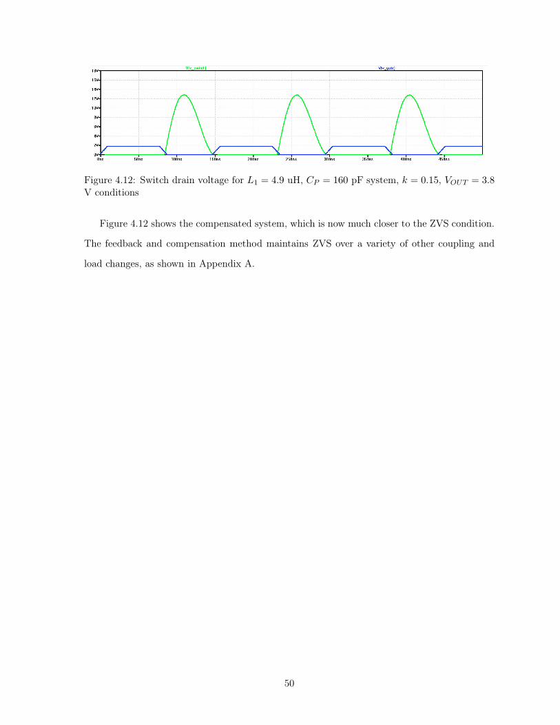
Figure 4.12: Switch drain voltage for L1 = 4.9 uH, CP = 160 pF system, k = 0.15, VOUT = 3.8V conditions
Figure 4.12 shows the compensated system, which is now much closer to the ZVS condition.
The feedback and compensation method maintains ZVS over a variety of other coupling and
load changes, as shown in Appendix A.
50
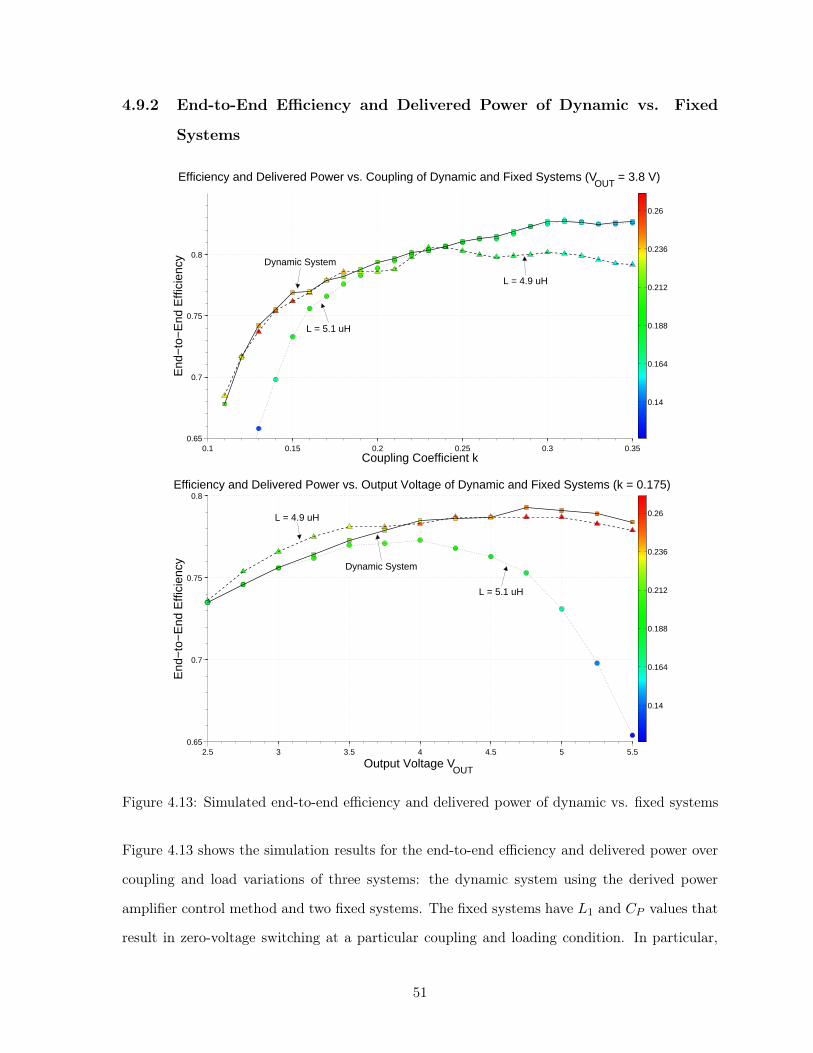
4.9.2 End-to-End Efficiency and Delivered Power of Dynamic vs. Fixed
Systems
0.1 0.15 0.2 0.25 0.3 0.350.65
0.7
0.75
0.8
Coupling Coefficient k
End
−to
−E
nd E
ffici
ency
Efficiency and Delivered Power vs. Coupling of Dynamic and Fixed Systems (VOUT
= 3.8 V)
0.14
0.164
0.188
0.212
0.236
0.26
L = 4.9 uH
L = 5.1 uH
Dynamic System
2.5 3 3.5 4 4.5 5 5.50.65
0.7
0.75
0.8
Output Voltage VOUT
End
−to
−E
nd E
ffici
ency
Efficiency and Delivered Power vs. Output Voltage of Dynamic and Fixed Systems (k = 0.175)
0.14
0.164
0.188
0.212
0.236
0.26
L = 5.1 uH
Dynamic System
L = 4.9 uH
Figure 4.13: Simulated end-to-end efficiency and delivered power of dynamic vs. fixed systems
Figure 4.13 shows the simulation results for the end-to-end efficiency and delivered power over
coupling and load variations of three systems: the dynamic system using the derived power
amplifier control method and two fixed systems. The fixed systems have L1 and CP values that
result in zero-voltage switching at a particular coupling and loading condition. In particular,
51

one system has L1 = 4.9 uH and CP = 88 pF, while the other system has L1 = 5.1 uH and
CP = 48 pF. The delivered power levels are those seen at the load, and they are represented by
the color of each data point in the plot.
The dynamic system has clear advantages over the fixed systems. First, for low coupling
and high output voltage conditions, the efficiency and delivered power of the 5.1 uH fixed
system drops drastically due to the power factor of the circuit being increasingly less than one,
while the dynamic system follows the 4.9 uH fixed system curves. Second, for high coupling
conditions, the efficiency of the 4.9 uH fixed system drops significantly due to losses caused by
output capacitor discharge at switch turn-on, while the dynamic system follows the 5.1 uH fixed
system curve. Third, for relatively low coupling and relatively high output voltage conditions,
the delivered power of the 4.9 uH fixed system increases drastically due to the relatively low
shunt capacitance and high Q, while the dynamic system delivered power is balanced between
the 4.9 uH and 5.1 uH fixed system delivered power levels. Essentially, the power amplifier
control method adjusts the system to match the performance of the best fixed system for a
given coupling and load condition.
4.10 Summary of Theoretical Analysis of Design for Efficiency
and Power
The last three chapters present a theoretical analysis of the power amplifier control loop for
the wireless charging system in this work. The design enables the system to achieve over 75%
nominal end-to-end efficiency transferring ∼ 170 mW over 9 mm. The design also enables
the system to maintain this high efficiency and regulate the delivered power as the coupling
coefficient and output voltage conditions change. The system does this by actively monitoring
the Class-E power amplifier switch drain voltage at the time of switch turn-on to check if the
power amplifier is in the zero-voltage switching condition. If not, the system compensates by
adjusting the primary coil inductance and shunt capacitance to bring the power amplifier back
towards the zero-voltage switching condition while maintaining the delivered power level.
The following chapters present the design and implementation of this enhanced wireless
charging system, starting with IC design and continuing with PCB system design.
52
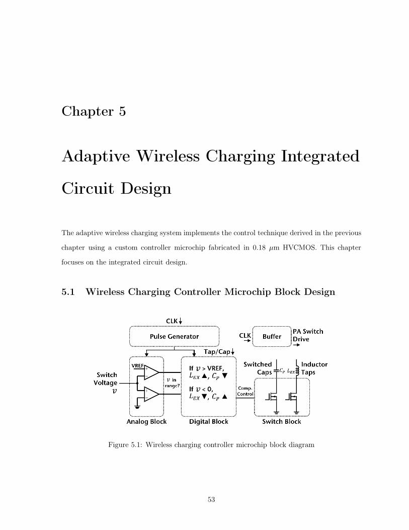
Chapter 5
Adaptive Wireless Charging Integrated
Circuit Design
The adaptive wireless charging system implements the control technique derived in the previous
chapter using a custom controller microchip fabricated in 0.18 µm HVCMOS. This chapter
focuses on the integrated circuit design.
5.1 Wireless Charging Controller Microchip Block Design
Figure 5.1: Wireless charging controller microchip block diagram
53

Figure 5.1 shows a block diagram of the wireless charging controller microchip. The chip is
broken up into five main parts: the power amplifier switch drive buffer, the pulse generator
block, the analog block, the digital block, and the switch block.
The power amplifier switch drive buffer takes in an external clock signal and buffers it on
chip to drive the external power amplifier switch gate.
The pulse generator block takes in the same external clock signal and extracts a single pulse
about every millisecond to trigger the analog and digital blocks. Thus, the adaptive control
activates about every millisecond. This is fast enough to allow the system to react to changing
conditions rapidly and also slow enough to ensure stability.
The input signal, which is the power amplifier switch drain voltage, flows through the
analog, digital, and switch blocks in series to the output. The analog block determines if the
drain voltage at switch turn-on is sufficiently close to zero. Then the digital block determines
if compensation of the power amplifier is needed. If so, the switch block handles adjusting the
tunable power amplifier shunt capacitance and resonant tank inductance.
The following sections detail the design of each of the blocks on the chip.
5.2 Microchip Power Amplifier Switch Drive Buffer Design
The power amplifier switch drive buffer drives the gate of the external power amplifier switch.
The input is an externally generated 3.3 V 6.78 MHz clock that is level shifted to 1.8 V on chip.
This level-shifted fast clock signal FCLK is buffered through an inverter chain to drive the
∼ 100 pF input capacitance of the power amplifier switch. FCLK is also routed as an input
to the pulse generator block.
Due to the inverter chain delay, the power amplifier switch drive signal DRIV E is a delayed
version of FCLK. In simulation, the delay from the rising edge of FCLK to the moment
DRIV E starts to rise is 2.1 ns in the fastest case. The delay from the rising edge of FCLK to
the point DRIV E is 67% of its final value is 8.2 ns in the fastest case.
54
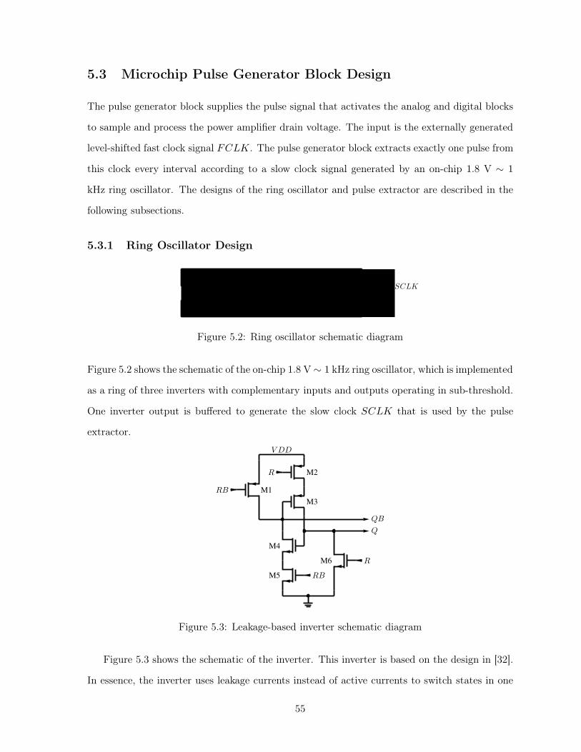
5.3 Microchip Pulse Generator Block Design
The pulse generator block supplies the pulse signal that activates the analog and digital blocks
to sample and process the power amplifier drain voltage. The input is the externally generated
level-shifted fast clock signal FCLK. The pulse generator block extracts exactly one pulse from
this clock every interval according to a slow clock signal generated by an on-chip 1.8 V ∼ 1
kHz ring oscillator. The designs of the ring oscillator and pulse extractor are described in the
following subsections.
5.3.1 Ring Oscillator Design
R
RB
Q
QB
R
RB
Q
QB
R
RB
Q
QB
SCLK
Figure 5.2: Ring oscillator schematic diagram
Figure 5.2 shows the schematic of the on-chip 1.8 V ∼ 1 kHz ring oscillator, which is implemented
as a ring of three inverters with complementary inputs and outputs operating in sub-threshold.
One inverter output is buffered to generate the slow clock SCLK that is used by the pulse
extractor.
M1RB
M3
M2R
VDD
M4
M5 RB
Q
M6 R
QB
Figure 5.3: Leakage-based inverter schematic diagram
Figure 5.3 shows the schematic of the inverter. This inverter is based on the design in [32].
In essence, the inverter uses leakage currents instead of active currents to switch states in one
55
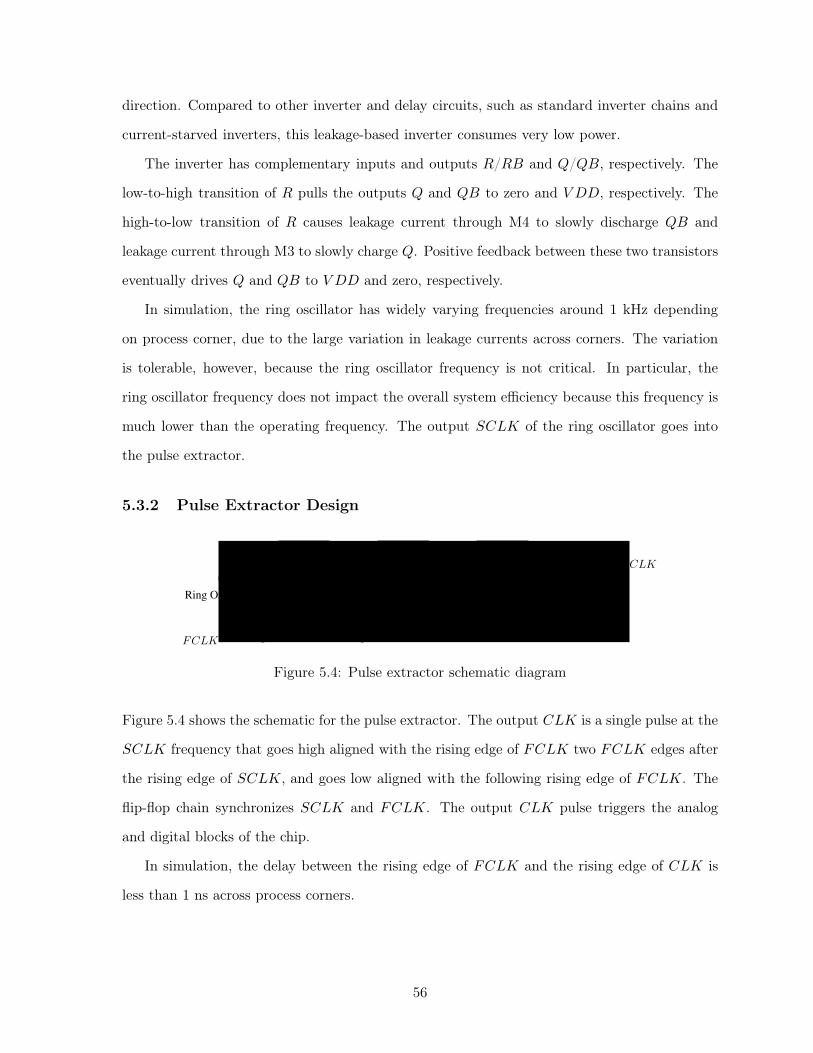
direction. Compared to other inverter and delay circuits, such as standard inverter chains and
current-starved inverters, this leakage-based inverter consumes very low power.
The inverter has complementary inputs and outputs R/RB and Q/QB, respectively. The
low-to-high transition of R pulls the outputs Q and QB to zero and V DD, respectively. The
high-to-low transition of R causes leakage current through M4 to slowly discharge QB and
leakage current through M3 to slowly charge Q. Positive feedback between these two transistors
eventually drives Q and QB to V DD and zero, respectively.
In simulation, the ring oscillator has widely varying frequencies around 1 kHz depending
on process corner, due to the large variation in leakage currents across corners. The variation
is tolerable, however, because the ring oscillator frequency is not critical. In particular, the
ring oscillator frequency does not impact the overall system efficiency because this frequency is
much lower than the operating frequency. The output SCLK of the ring oscillator goes into
the pulse extractor.
5.3.2 Pulse Extractor Design
Ring Osc
Q1
Q
Q
CK
D
FCLK
Q2
Q
Q
CK
D
Q3
Q
Q
CK
DCLK
Figure 5.4: Pulse extractor schematic diagram
Figure 5.4 shows the schematic for the pulse extractor. The output CLK is a single pulse at the
SCLK frequency that goes high aligned with the rising edge of FCLK two FCLK edges after
the rising edge of SCLK, and goes low aligned with the following rising edge of FCLK. The
flip-flop chain synchronizes SCLK and FCLK. The output CLK pulse triggers the analog
and digital blocks of the chip.
In simulation, the delay between the rising edge of FCLK and the rising edge of CLK is
less than 1 ns across process corners.
56
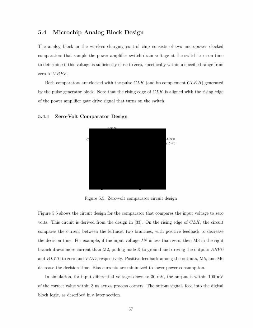
5.4 Microchip Analog Block Design
The analog block in the wireless charging control chip consists of two micropower clocked
comparators that sample the power amplifier switch drain voltage at the switch turn-on time
to determine if this voltage is sufficiently close to zero, specifically within a specified range from
zero to V REF .
Both comparators are clocked with the pulse CLK (and its complement CLKB) generated
by the pulse generator block. Note that the rising edge of CLK is aligned with the rising edge
of the power amplifier gate drive signal that turns on the switch.
5.4.1 Zero-Volt Comparator Design
M1CLKB
M2 M3
IN
M4CLKB
VDD
M5
M6
CLKB
Z
ABV 0
BLW0
Figure 5.5: Zero-volt comparator circuit design
Figure 5.5 shows the circuit design for the comparator that compares the input voltage to zero
volts. This circuit is derived from the design in [33]. On the rising edge of CLK, the circuit
compares the current between the leftmost two branches, with positive feedback to decrease
the decision time. For example, if the input voltage IN is less than zero, then M3 in the right
branch draws more current than M2, pulling node Z to ground and driving the outputs ABV 0
and BLW0 to zero and V DD, respectively. Positive feedback among the outputs, M5, and M6
decrease the decision time. Bias currents are minimized to lower power consumption.
In simulation, for input differential voltages down to 30 mV, the output is within 100 mV
of the correct value within 3 ns across process corners. The output signals feed into the digital
block logic, as described in a later section.
57
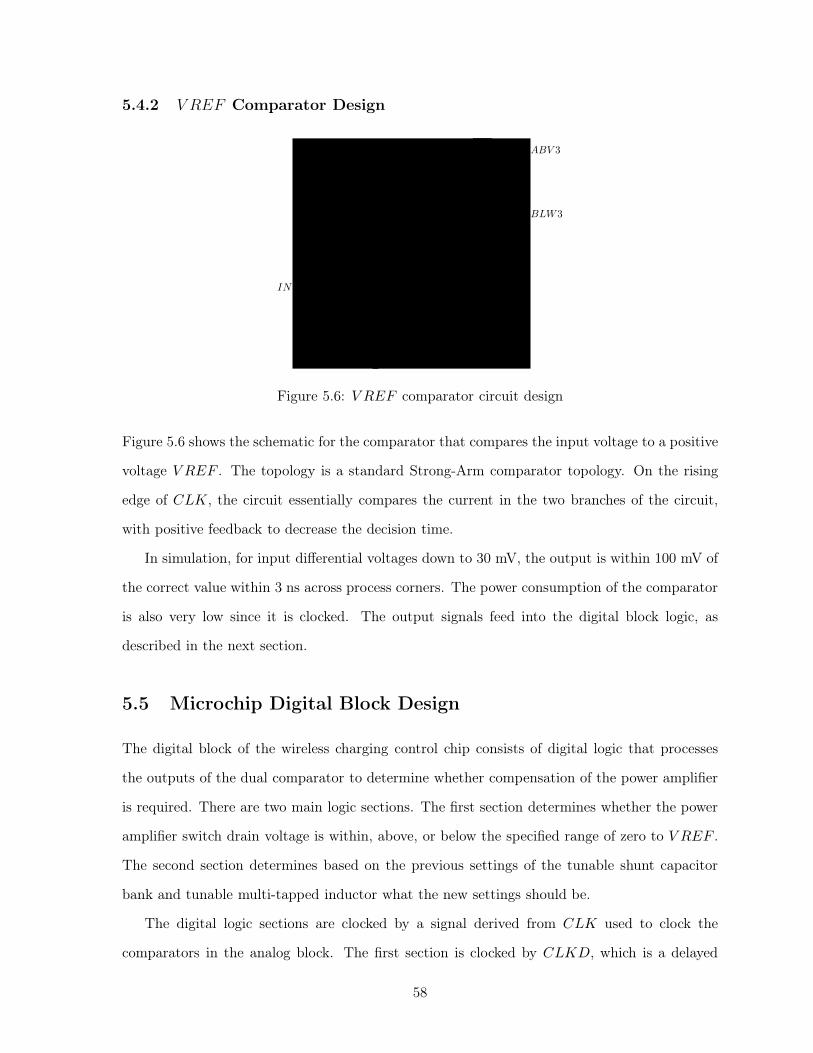
5.4.2 V REF Comparator Design
M1
M2
V DD
M3
M4
ZZB
ZZ
M5IN M6 V REF
M7CLK
X Y
BLW3
ABV 3
Figure 5.6: V REF comparator circuit design
Figure 5.6 shows the schematic for the comparator that compares the input voltage to a positive
voltage V REF . The topology is a standard Strong-Arm comparator topology. On the rising
edge of CLK, the circuit essentially compares the current in the two branches of the circuit,
with positive feedback to decrease the decision time.
In simulation, for input differential voltages down to 30 mV, the output is within 100 mV of
the correct value within 3 ns across process corners. The power consumption of the comparator
is also very low since it is clocked. The output signals feed into the digital block logic, as
described in the next section.
5.5 Microchip Digital Block Design
The digital block of the wireless charging control chip consists of digital logic that processes
the outputs of the dual comparator to determine whether compensation of the power amplifier
is required. There are two main logic sections. The first section determines whether the power
amplifier switch drain voltage is within, above, or below the specified range of zero to V REF .
The second section determines based on the previous settings of the tunable shunt capacitor
bank and tunable multi-tapped inductor what the new settings should be.
The digital logic sections are clocked by a signal derived from CLK used to clock the
comparators in the analog block. The first section is clocked by CLKD, which is a delayed
58
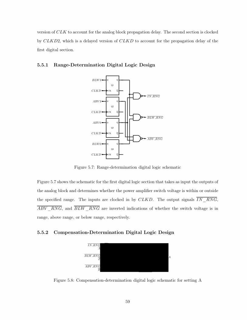
version of CLK to account for the analog block propagation delay. The second section is clocked
by CLKD2, which is a delayed version of CLKD to account for the propagation delay of the
first digital section.
5.5.1 Range-Determination Digital Logic Design
Q1
Q
Q
CK
D
Q2
Q
Q
CK
D
Q3
Q
Q
CK
D
Q4
Q
Q
CK
D
CLKD
CLKD
CLKD
CLKD
BLW3
ABV 3
ABV 0
BLW0
IN RNG
BLW RNG
ABV RNG
Figure 5.7: Range-determination digital logic schematic
Figure 5.7 shows the schematic for the first digital logic section that takes as input the outputs of
the analog block and determines whether the power amplifier switch voltage is within or outside
the specified range. The inputs are clocked in by CLKD. The output signals IN_RNG,
ABV _RNG, and BLW_RNG are inverted indications of whether the switch voltage is in
range, above range, or below range, respectively.
5.5.2 Compensation-Determination Digital Logic Design
IN RNGA
BLW RNGZ
ABV RNGB
Q1
Q
Q
CK
D
CLKD2
AA
Figure 5.8: Compensation-determination digital logic schematic for setting A
59

Figure 5.8 shows the schematic for a part of the second digital logic section that takes as input
the outputs of the first digital logic section as well as the previous settings of both the shunt
capacitor and multi-tapped inductor, and determines how to update these settings. As detailed
in Section 4.7, there are five settings corresponding to five combinations of power amplifier
shunt capacitance and resonant tank inductance, as shown in Table 5.1 from highest to lowest
(highest to lowest capacitance). At each rising edge of CLKD2, exactly one setting out of five
is chosen.
Compensation Setting Excess Inductance LEX Shunt Capacitance CP
D 0.7 uH 240 pF
C 0.75 uH 190 pF
B 0.8 uH 160 pF
A 0.85 uH 140 pF
Z 0.9 uH 130 pF
Table 5.1: Tunable excess inductance and shunt capacitance values used in design
The schematic in Figure 5.8 shows the circuit to choose setting A. The inputs to this circuit
are IN_RNG, ABV _RNG, and BLW_RNG from the first digital logic block, and Z, A,
and B, with information on whether the previous setting was Z, A, or B.
In general, this digital logic chooses a given setting if one of the following conditions is true:
• The setting was the previous setting and the switch voltage is in range
• The previous setting was one setting lower and the switch voltage is below range
• The previous setting was one setting higher and the switch voltage is above range
The logic follows this format for choosing any of the settings from A to D. Note that in the
logic for choosing D, the third condition does not exist. Instead, the third condition is that if
the switch voltage is below range and the previous setting was D, the new setting is still D.
AB
CD
Z
Z
Figure 5.9: Compensation-determination digital logic schematic for setting Z
60
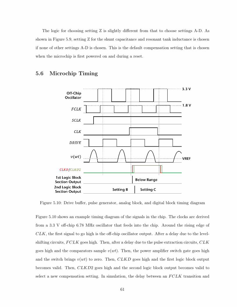
The logic for choosing setting Z is slightly different from that to choose settings A-D. As
shown in Figure 5.9, setting Z for the shunt capacitance and resonant tank inductance is chosen
if none of other settings A-D is chosen. This is the default compensation setting that is chosen
when the microchip is first powered on and during a reset.
5.6 Microchip Timing
Figure 5.10: Drive buffer, pulse generator, analog block, and digital block timing diagram
Figure 5.10 shows an example timing diagram of the signals in the chip. The clocks are derived
from a 3.3 V off-chip 6.78 MHz oscillator that feeds into the chip. Around the rising edge of
CLK, the first signal to go high is the off-chip oscillator output. After a delay due to the level-
shifting circuits, FCLK goes high. Then, after a delay due to the pulse extraction circuits, CLK
goes high and the comparators sample v(wt). Then, the power amplifier switch gate goes high
and the switch brings v(wt) to zero. Then, CLKD goes high and the first logic block output
becomes valid. Then, CLKD2 goes high and the second logic block output becomes valid to
select a new compensation setting. In simulation, the delay between an FCLK transition and
61
transition of a new setting is about 8 ns.
In this example, on the rising edge of CLKD, v(wt) is below range as sampled on the rising
edge of CLK, so BLW_RNG goes low. On the rising edge of CLKD2, since the previous
setting was B, the second logic block adjusts the new setting to C.
One critical timing constraint is that the rising edge of CLK must come before the rising
edge of the power switch gate drive. This is so the comparators in the analog block can correctly
sample the switch voltage before the switch turns on. The other critical timing constraints are
that the delay from CLK to CLKD and the delay from CLKD to CLKD2 must be greater than
the propagation delay of the analog block and the first digital logic block section, respectively.
These constraints are ensured through simulation across corners.
5.7 Microchip Switch Block Design
The switch block circuits implement the setting chosen by the digital logic block by controlling
the tuning of the power amplifier shunt capacitance and resonant inductance. The shunt capaci-
tance is made up of a bank of five capacitors while the resonant tank inductance is implemented
as a multi-tapped coil with five taps.
A B C D
v(wt)
Figure 5.11: Tunable power amplifier shunt capacitance schematic diagram
62

v(wt)
· · ·
V DD · · ·
D Z· · ·
Figure 5.12: Tunable resonant tank inductance schematic diagram
Figures 5.11 and 5.12 show the schematic for the tunable shunt capacitance and resonant
inductance. The components below the dashed line in each figure are on chip, while the com-
ponents above the dashed line are off chip.
The fixed capacitor in Figure 5.11 has capacitance corresponding to the setting Z in Table
5-1, minus the parasitic output capacitance of the power amplifier switch and diode (about 100
pF in simulation). Each of the other switchable capacitors in Figure 5.11 are sized such that
when the capacitor for a given setting is switched into the circuit, the total shunt capacitance
is the correct value as specified in Table 5.1.
On the chip, four high-voltage power MOSFETs control switching each of the capacitors for
settings A-D into and out of the circuit. The switches are sized proportional to the capacitance
of the associated off-chip capacitors, so that the off-state capacitance and on-state resistance
are proportional to the associated capacitance.
The taps on the multi-tapped resonant inductor, as shown in Figure 5.12, are controlled by
off-chip solid-state relays. This design is similar to that reported in [19]. Relays are used instead
of MOSFETs due to their ability to block the AC voltage and current present in the inductor.
The inductance between each tap is 50 nH, so the chip can tune the resonant inductance in
increments of 50 nH between 4.9 µH and 5.1 µH according to Table 5.1. On the chip, five
identical high-voltage power MOSFETs turn on and off the control currents for the relays.
63

5.8 Chapter Summary
This chapter presents the design of an integrated circuit for implementing the power amplifier
control loop derived from mathematical analysis. At a rate determined by the pulse generator
block, the chip samples the power amplifier switch drain voltage at switch turn-on and compares
it to a specified range between 0 and V REF to determine if the power amplifier is in the zero-
voltage switching condition. If not, the chip changes the compensation setting, determined
by the digital block and implemented by the switch block, to bring the power amplifier back
towards ZVS while maintaining power levels. The next chapter details how this chip is used in
a full wireless charging system.
64
Chapter 6
Adaptive Wireless Charging System
Design
This chapter describes the PCB design incorporating the microchip from Chapter 5 into a
complete adaptive portable-to-portable resonant inductive wireless charging system operating
at 6.78 MHz.
3.3 V
LCHOKE
M1DRIV E D1 M2
Analog In
D2
CP · · ·
Caps
C1
L1 L2
Taps
· · · k:n
C2
COUT
+vOUT− Load
Wireless Charging Control Chip
3.3 V, 1.8 V
V REF
6.78 MHz
DRIV E
Buck Converter3.3 V 1.8 V Oscillator 6.78 MHz Reference V REF
Figure 6.1: Full wireless charging system diagram
Figure 6.1 shows the full wireless charging system including the wireless power circuit of
Chapter 2, the wireless charging control chip of Chapter 5, and accessory circuits for the chip.
65
Energy is transferred from the 3.3 V source in the transmitter device to the ultra-capacitor in
the receiver device, which powers the load. The following sections describe the implementation
of each of the blocks in the wireless charging system, with focus on the power loss of each of
the components.
6.1 Wireless Power Circuit Implementation
6.1.1 Class-E Power Amplifier Implementation
The Class-E power amplifier components LCHOKE, M1, D1, and CP are selected to maximize
nominal efficiency of the power amplifier.
The choke inductor maintains constant current from the battery to the power amplifier, and
thus must have high inductance with low conduction loss. LCHOKE is chosen to be 22 µH with
a DC resistance of 100 mΩ. For 200 mW nominal power drawn from the source, the constant
current flowing through the choke inductor is 200/3.3 ≈ 60 mA, so the average power loss is
0.062 × 0.1 ≈ 0.4 mW, which is negligible compared to the delivered power.
The MOSFET M1 switches at the 6.78 MHz operating frequency to generate the AC current
to drive the primary resonant tank. It must have low input capacitance and low on-resistance
for low switching and conduction losses. A parallel combination of two Si1012CR MOSFETs
is chosen that optimizes this tradeoff. M1 has a total input capacitance of 100 pF and an on-
resistance of 0.4 Ω (each MOSFET) at a drive strength of 1.8 V. Thus, the combined MOSFET
M1 has a switching loss of 100× 10−12 × 1.82 × 6.78× 106 ≈ 2.2 mW. From simulation, M1 has
a conduction loss of 3.2 mW.
The purpose of the shunt diode D1 is to clamp the switch drain voltage v(wt) at a voltage
very close to zero, to prevent the body diode of M1 from turning on. This avoids loss because
the body diode ordinarily has a high forward voltage. The Schottky diode DB2J209, with a
forward voltage of 0.28 V at 60 mA forward current, is chosen. Since the forward voltage is
small and little current flows through the diode, the power loss due to D1 is negligible.
The shunt capacitors CP are originally sized according to the design values in Table 5.1,
but in testing the capacitances are slightly modified to optimize performance.
66
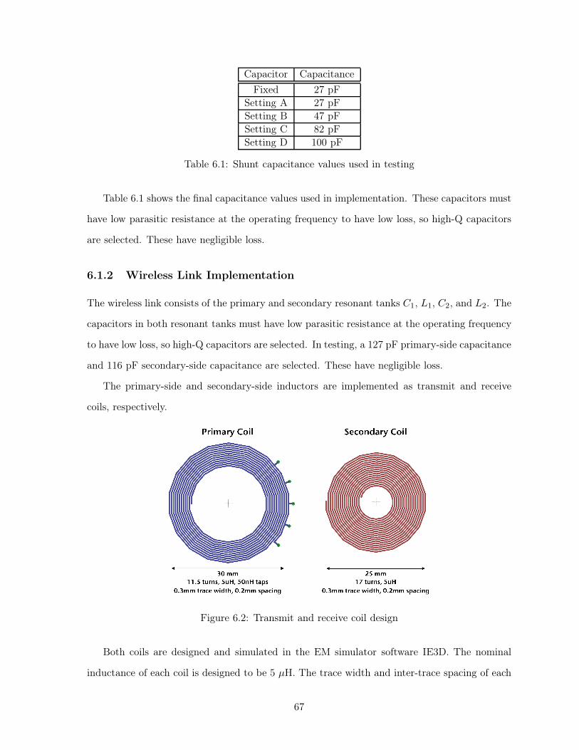
Capacitor Capacitance
Fixed 27 pF
Setting A 27 pF
Setting B 47 pF
Setting C 82 pF
Setting D 100 pF
Table 6.1: Shunt capacitance values used in testing
Table 6.1 shows the final capacitance values used in implementation. These capacitors must
have low parasitic resistance at the operating frequency to have low loss, so high-Q capacitors
are selected. These have negligible loss.
6.1.2 Wireless Link Implementation
The wireless link consists of the primary and secondary resonant tanks C1, L1, C2, and L2. The
capacitors in both resonant tanks must have low parasitic resistance at the operating frequency
to have low loss, so high-Q capacitors are selected. In testing, a 127 pF primary-side capacitance
and 116 pF secondary-side capacitance are selected. These have negligible loss.
The primary-side and secondary-side inductors are implemented as transmit and receive
coils, respectively.
Figure 6.2: Transmit and receive coil design
Both coils are designed and simulated in the EM simulator software IE3D. The nominal
inductance of each coil is designed to be 5 µH. The trace width and inter-trace spacing of each
67
coil are varied to determine their effects on coil inductance, which is found to be small. The
trace width and trace thickness have effects on the coil ESR, however, which influences the
power loss of the coils. Both coils are designed with a 0.3 mm trace width, 2-oz copper trace
thickness, and 0.2 mm inter-trace spacing. This results in coil ESR of about 1.5 Ω each. In
simulation the primary-side coil power loss is about 10 mW and the secondary-side coil power
loss is about 5 mW. Both of these losses are major contributors to the nominal efficiency and
are considered in the nominal efficiency calculation in Section 4.8.
The secondary coil is a fixed inductance and is designed with 17 turns for a nominal induc-
tance of 5 µH. In testing the inductance is found to be 4.8 µH. The primary coil is a five-tap
coil and is designed with 11.5 turns for a nominal inductance of 5 µH for the middle tap and
50 nH inductance difference between taps. In testing the nominal inductance is found to be 5.1
µH.
The relays to switch in the taps must have low on-resistance and off-capacitance for low
power loss when on and low parasitic effects when off. The G3VM-21LR11 relay is chosen to
optimize this RxC tradeoff. Each relay has an on-resistance of 0.27 Ω at 1.7 mA drive current
and an off-capacitance of 40 pF. The on-resistance is much lower than the ESR of the in-series
primary-side coil, so the power loss when on is negligible. The off-capacitance is much lower
than the capacitance of the in-series resonant capacitance, so the off-state parasitic effects are
negligible.
As shown in Figure 5.12, the control current for each relay is set by a resistor to 1.7 mA
to balance the on-resistance of the relay with the power dissipation of the control circuit. This
power dissipation is 0.0017× 1.8 ≈ 3 mW. A 10 uF capacitor in parallel with the resistor allows
high in-rush current when the relay turns on so that it may turn on faster. The turn-on time
of each relay is 20 µs while the turn-off time is 100 µs. Note that the turn-on time is less than
the turn-off time so that there is never a time when no relays are on (in that case, the current
through the primary-side inductor would not have a path to flow).
6.1.3 Rectifier Implementation
The full-wave rectifier consists of four discrete Schottky diodes. These diodes must have low
forward voltage for low power loss when on. The average diode current for an output power of
68
200 mW and a typical output voltage of 3.8 V is about 53 mA. The PMEG2005AELD diode is
chosen, with a forward voltage of 0.18 V at this current. Thus, the average power loss for each
diode is 0.053× 0.18 ≈ 10 mW. Since two diodes are on at any given time, the total power loss
is about 20 mW, for a rectifier efficiency of about 90%.
Lower power loss may be achieved by using a CMOS rectifier, by replacing the discrete diode
devices with MOSFETs with lower conduction voltage drops. This is not explored in the tested
system but is the subject of extensive research [26, 27, 28, 29, 30].
6.1.4 Load Implementation
The rectifier is loaded by an ultra-capacitor that charges up from 2.5 V to 5 V as it receives
power. The ultra-capacitor must have low ESR for low power loss when charging. For testing,
a 3 F 5 V ultra-capacitor is selected with an ESR of 75 mΩ. The power loss due to such a low
ESR is negligible.
6.1.5 Wireless Power Circuit Implementation Summary
Component Implementation
Choke Inductor 744053220 power inductor
M1 Si1012CR NMOS (2 in parallel)
D1 DB2J209 Schottky diode
Shunt Capacitors Johanson Technology S-Series high-Q capacitors
Resonant Capacitors Johanson Technology S-Series high-Q capacitors
Rectifier Diodes PMEG2005AELD Schottky diodes
Output Storage Capacitor PHV-5R4H305-R ultra-capacitor
Table 6.2: Wireless power circuit components used in testing
Table 6.2 summarizes the components used in the wireless power circuit.
6.2 Wireless Charging Control Chip Implementation
The wireless charging control chip described in Chapter 5 is packaged in a 48-lead TQFP
package. The supplies, inputs, and outputs of the packaged chip are described in the following
subsections. A chip pinout is included in Appendix B.
69
6.2.1 Chip Supplies
The voltage supplies for the chip include a high-voltage 3.3 V supply V CC for driving the power
switches of the switch block and a low-voltage 1.8 V supply V DD for the on-chip analog and
digital logic.
6.2.2 Chip Inputs
The three main signal inputs to the chip are the analog input IN for the switch voltage v(wt),
the reference voltage V REF , and the external 6.78 MHz oscillator clock OSC. The analog input
is generated from v(wt) by passing this voltage through a protection MOSFET M2 and diode
D2. These two components are designed to restrict the analog input voltage to a maximum of
V CC = 3.3 V, since the on-chip input transistors for the analog input are rated for 3.3 V. The
MOSFET must have short turn-on and turn-off times and the diode must have low forward
drop for effective clamping. The Si1062X MOSFET is chosen to be M2, with a typical turn-on
and turn-off time of 2 and 16 ns, respectively. The PMEG2005AELD Schottky diode is chosen
to be D2, with less than a 50 mV forward voltage drop at the microamp-level input currents of
the analog input.
The reference voltage V REF is generated by an external resistor divider sourced from V CC.
The clock signal is generated from an external silicon oscillator.
6.2.3 Chip Outputs
The chip drives the main power amplifier switch M1 with a 1.8 V clock signal at 6.78 MHz. The
chip also includes several control outputs for adjusting the power amplifier, four for switching
the CP shunt capacitor bank and five for switching the L1 transmit coil tap relays.
6.3 Accessory Circuit Implementation
6.3.1 1.8 V V DD Buck Converter Implementation
A 3.3 V-to-1.8 V buck converter is chosen to supply to the on-chip analog and digital circuits and
the relay control circuits. Together, these circuits draw about 1.7 mA on average (dominated
70

by the relay control current). The buck converter must be efficient at this output current to
minimize power loss. The TPS62202 converter is chosen, with 92% efficiency.
6.3.2 6.78 MHz Oscillator Implementation
The on-board 6.78 MHz oscillator supplies the clock signal for the wireless charging controller
chip. The oscillator must be efficient at the 3.3 V supply voltage V CC. The LTC6900 is chosen,
with a supply current of 0.9 mA.
It is important that the oscillator starts up only after one of the relays in the wireless power
circuit is on. Otherwise, the power amplifier builds up current in the choke inductor that has
no path to flow when the power amplifier switch is off. Since the oscillator runs off V CC while
the relays run off V DD, which is derived from V CC through a buck converter, there is a period
of time when V CC is stable but V DD is not stable. To avoid the associated race condition,
the AP2280-2 power switch is added between V CC and the supply input of the oscillator to
turn on the oscillator only after V DD is stable for 1 ms. This allows a relay to fully turn on
before the oscillator starts up.
6.4 Board Design Considerations
In this work, wireless charging systems are designed with two different transmitters. The first
transmitter is for testing purposes, with all signals routed to test points, focusing on ease of
measurement. The 3.3 V supply V CC for the test transmitter is sourced from an external
power supply. The second transmitter is the prototype, focusing on a minimized form factor.
The prototype transmitter board includes a 30-pin connector to plug into an iPhone, and V CC
for the transmitter is sourced from the cell phone battery (specifically, on pin 18 of the 30-pin
connector).
For all transmitter and receiver board designs, a number of layout considerations are im-
portant for proper operation. These considerations are described in the following subsections.
71

6.4.1 Isolation to Transmit and Receive Coils
It is important for the transmit and receive coils to be physically isolated from surrounding
planes, traces, and circuitry. This is because a significant magnetic field is generated or received
by these coils, and this field can couple to other metal structures. As a result, the operation of
these structures can be impacted, or these structures can shield the magnetic field.
Metal planes, which are used in other areas of the PCB, are absent underneath the transmit
and receive coils. Traces supplying the control current to the relays for the taps on the transmit
coil are located as far away from the coil as possible. Sensitive circuitry such as the custom
chip and the oscillator are located as far away from the transmit coil as possible.
6.4.2 Undesired Inductance of Transmit and Receive Coils
The primary-side transmit and secondary-side receive coils are designed in simulation to have
a specific inductance. A specific series capacitance is matched to each coil so that each coil
resonates at a desired frequency. These resonant frequencies are significantly impacted by
undesired inductances of the traces leading to these coils. Thus, these trace inductances should
be minimized. To do this, the traces leading to the coils are made as short and wide as possible,
since inductance is proportional to trace length and inversely proportional to trace width.
Another source of undesired inductance is a wide open current loop. The main high-current
loops in the transmitter and receiver contain the currents going through the transmit and
receive coils. These loops are made as small as possible by decreasing trace lengths in these
loops through the use of ground planes, and by designing return current paths in a different
layer just underneath forward current paths.
A third source of undesired inductance is the shape of the routing to the transmit coil.
The routing to each of the taps of this multi-tapped coil affects the flux linkage. To keep
the inductance differential consistent between consecutive taps, a consistent radially symmetric
routing shape is implemented.
72

Figure 6.3: Trace routing to transmit coil
Figure 6.3 shows the layout of the trace routing to the primary-side transmit coil.
6.5 Chapter Summary
This chapter presents the design of a complete wireless charging system using the microchip
described in Chapter 5. The standard wireless power topology of Chapter 2 is used with the
microchip implementing closed-loop compensation of the Class-E power amplifier. The next
chapter presents measured performance results of this system with respect to the key metrics
of efficiency and power.
73
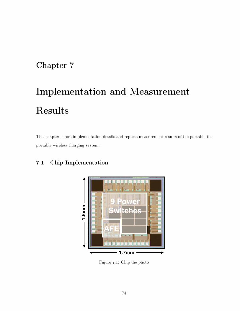
Chapter 7
Implementation and Measurement
Results
This chapter shows implementation details and reports measurement results of the portable-to-
portable wireless charging system.
7.1 Chip Implementation
Figure 7.1: Chip die photo
74
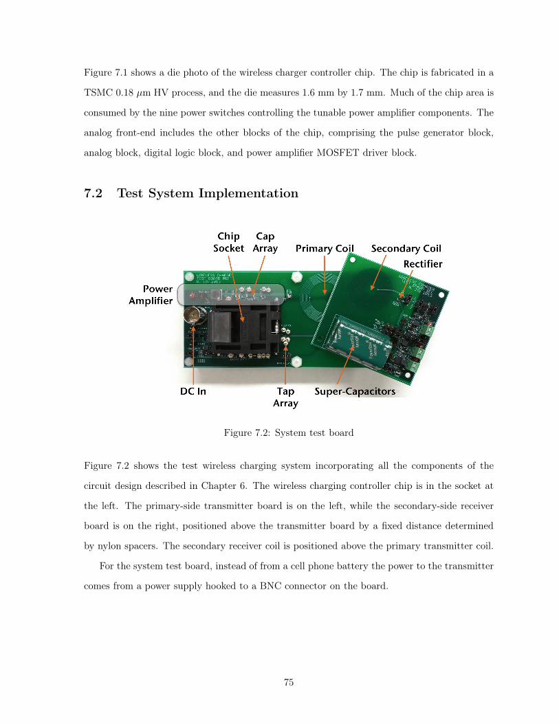
Figure 7.1 shows a die photo of the wireless charger controller chip. The chip is fabricated in a
TSMC 0.18 µm HV process, and the die measures 1.6 mm by 1.7 mm. Much of the chip area is
consumed by the nine power switches controlling the tunable power amplifier components. The
analog front-end includes the other blocks of the chip, comprising the pulse generator block,
analog block, digital logic block, and power amplifier MOSFET driver block.
7.2 Test System Implementation
Figure 7.2: System test board
Figure 7.2 shows the test wireless charging system incorporating all the components of the
circuit design described in Chapter 6. The wireless charging controller chip is in the socket at
the left. The primary-side transmitter board is on the left, while the secondary-side receiver
board is on the right, positioned above the transmitter board by a fixed distance determined
by nylon spacers. The secondary receiver coil is positioned above the primary transmitter coil.
For the system test board, instead of from a cell phone battery the power to the transmitter
comes from a power supply hooked to a BNC connector on the board.
75
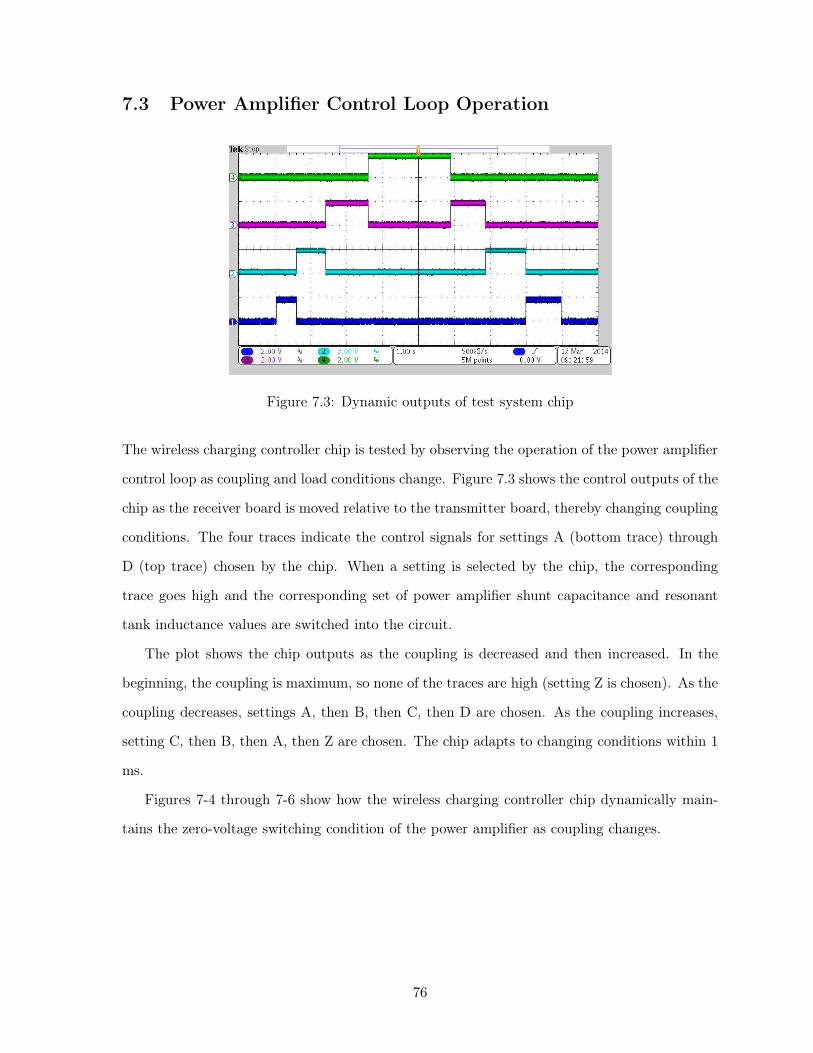
7.3 Power Amplifier Control Loop Operation
Figure 7.3: Dynamic outputs of test system chip
The wireless charging controller chip is tested by observing the operation of the power amplifier
control loop as coupling and load conditions change. Figure 7.3 shows the control outputs of the
chip as the receiver board is moved relative to the transmitter board, thereby changing coupling
conditions. The four traces indicate the control signals for settings A (bottom trace) through
D (top trace) chosen by the chip. When a setting is selected by the chip, the corresponding
trace goes high and the corresponding set of power amplifier shunt capacitance and resonant
tank inductance values are switched into the circuit.
The plot shows the chip outputs as the coupling is decreased and then increased. In the
beginning, the coupling is maximum, so none of the traces are high (setting Z is chosen). As the
coupling decreases, settings A, then B, then C, then D are chosen. As the coupling increases,
setting C, then B, then A, then Z are chosen. The chip adapts to changing conditions within 1
ms.
Figures 7-4 through 7-6 show how the wireless charging controller chip dynamically main-
tains the zero-voltage switching condition of the power amplifier as coupling changes.
76
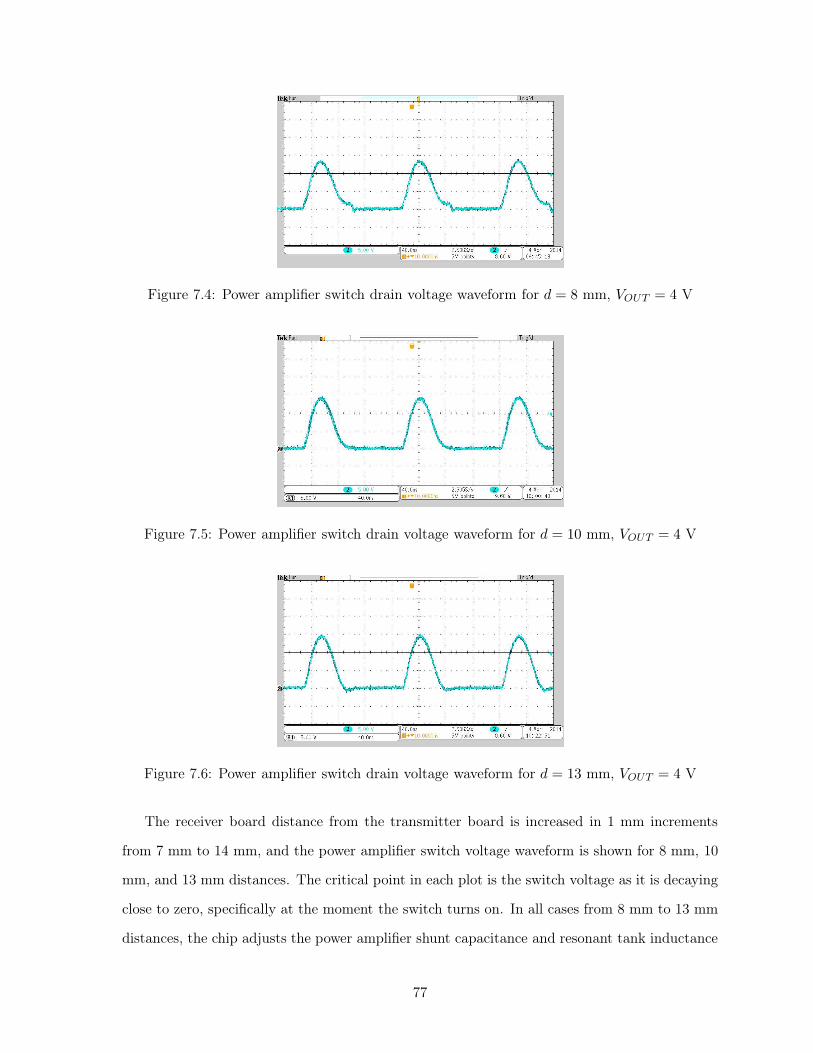
Figure 7.4: Power amplifier switch drain voltage waveform for d = 8 mm, VOUT = 4 V
Figure 7.5: Power amplifier switch drain voltage waveform for d = 10 mm, VOUT = 4 V
Figure 7.6: Power amplifier switch drain voltage waveform for d = 13 mm, VOUT = 4 V
The receiver board distance from the transmitter board is increased in 1 mm increments
from 7 mm to 14 mm, and the power amplifier switch voltage waveform is shown for 8 mm, 10
mm, and 13 mm distances. The critical point in each plot is the switch voltage as it is decaying
close to zero, specifically at the moment the switch turns on. In all cases from 8 mm to 13 mm
distances, the chip adjusts the power amplifier shunt capacitance and resonant tank inductance
77
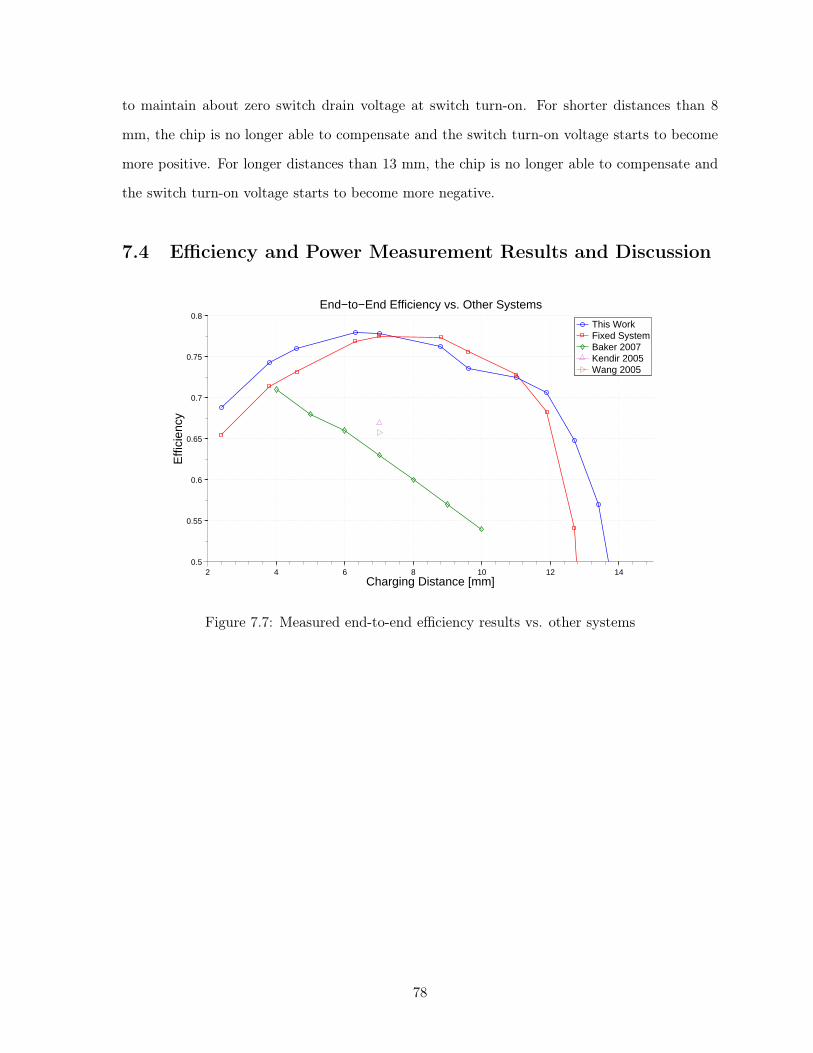
to maintain about zero switch drain voltage at switch turn-on. For shorter distances than 8
mm, the chip is no longer able to compensate and the switch turn-on voltage starts to become
more positive. For longer distances than 13 mm, the chip is no longer able to compensate and
the switch turn-on voltage starts to become more negative.
7.4 Efficiency and Power Measurement Results and Discussion
2 4 6 8 10 12 140.5
0.55
0.6
0.65
0.7
0.75
0.8
Charging Distance [mm]
Effi
cien
cy
End−to−End Efficiency vs. Other Systems
This Work Fixed System Baker 2007 Kendir 2005 Wang 2005
Figure 7.7: Measured end-to-end efficiency results vs. other systems
78
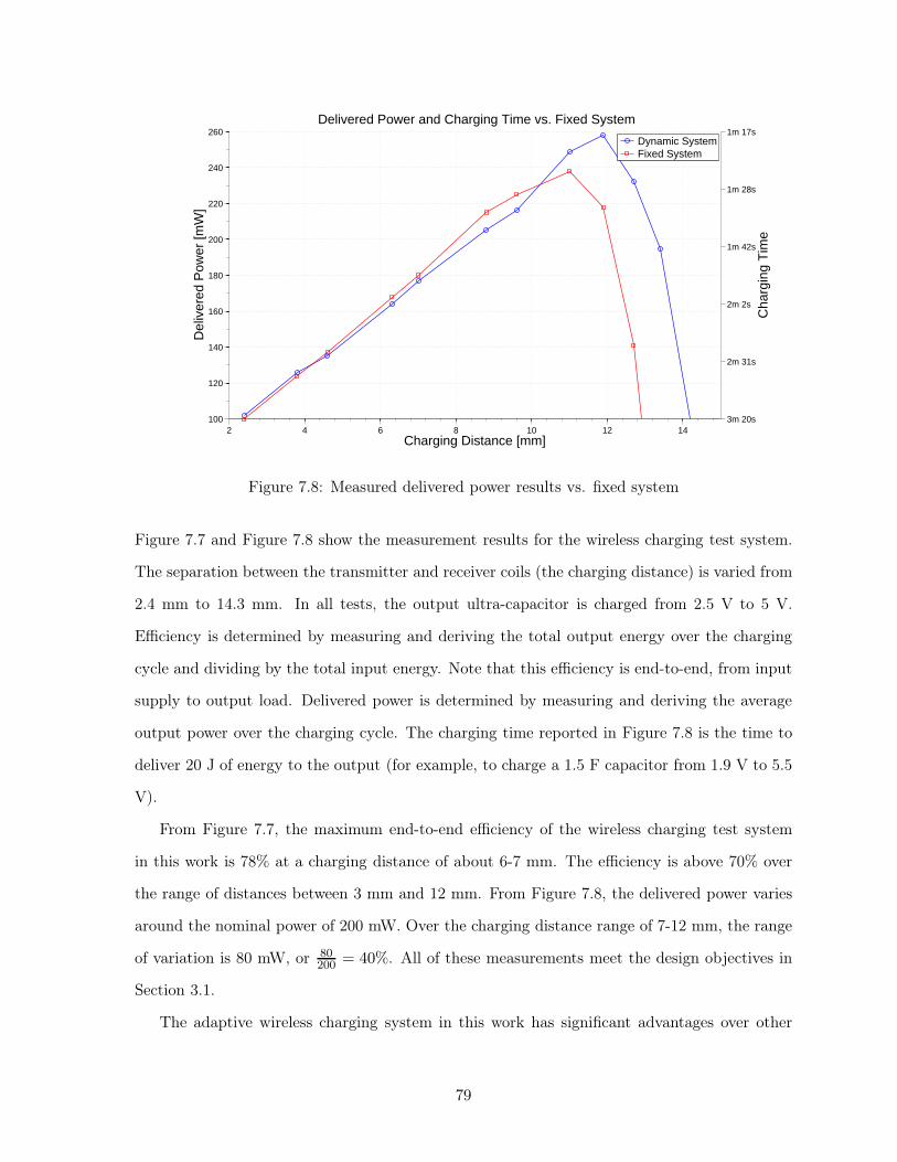
2 4 6 8 10 12 14100
120
140
160
180
200
220
240
260Delivered Power and Charging Time vs. Fixed System
Charging Distance [mm]
Del
iver
ed P
ower
[mW
]
Dynamic System Fixed System
1m 17s
1m 28s
1m 42s
2m 2s
2m 31s
3m 20s
Cha
rgin
g T
ime
Figure 7.8: Measured delivered power results vs. fixed system
Figure 7.7 and Figure 7.8 show the measurement results for the wireless charging test system.
The separation between the transmitter and receiver coils (the charging distance) is varied from
2.4 mm to 14.3 mm. In all tests, the output ultra-capacitor is charged from 2.5 V to 5 V.
Efficiency is determined by measuring and deriving the total output energy over the charging
cycle and dividing by the total input energy. Note that this efficiency is end-to-end, from input
supply to output load. Delivered power is determined by measuring and deriving the average
output power over the charging cycle. The charging time reported in Figure 7.8 is the time to
deliver 20 J of energy to the output (for example, to charge a 1.5 F capacitor from 1.9 V to 5.5
V).
From Figure 7.7, the maximum end-to-end efficiency of the wireless charging test system
in this work is 78% at a charging distance of about 6-7 mm. The efficiency is above 70% over
the range of distances between 3 mm and 12 mm. From Figure 7.8, the delivered power varies
around the nominal power of 200 mW. Over the charging distance range of 7-12 mm, the range
of variation is 80 mW, or 80200 = 40%. All of these measurements meet the design objectives in
Section 3.1.
The adaptive wireless charging system in this work has significant advantages over other
79
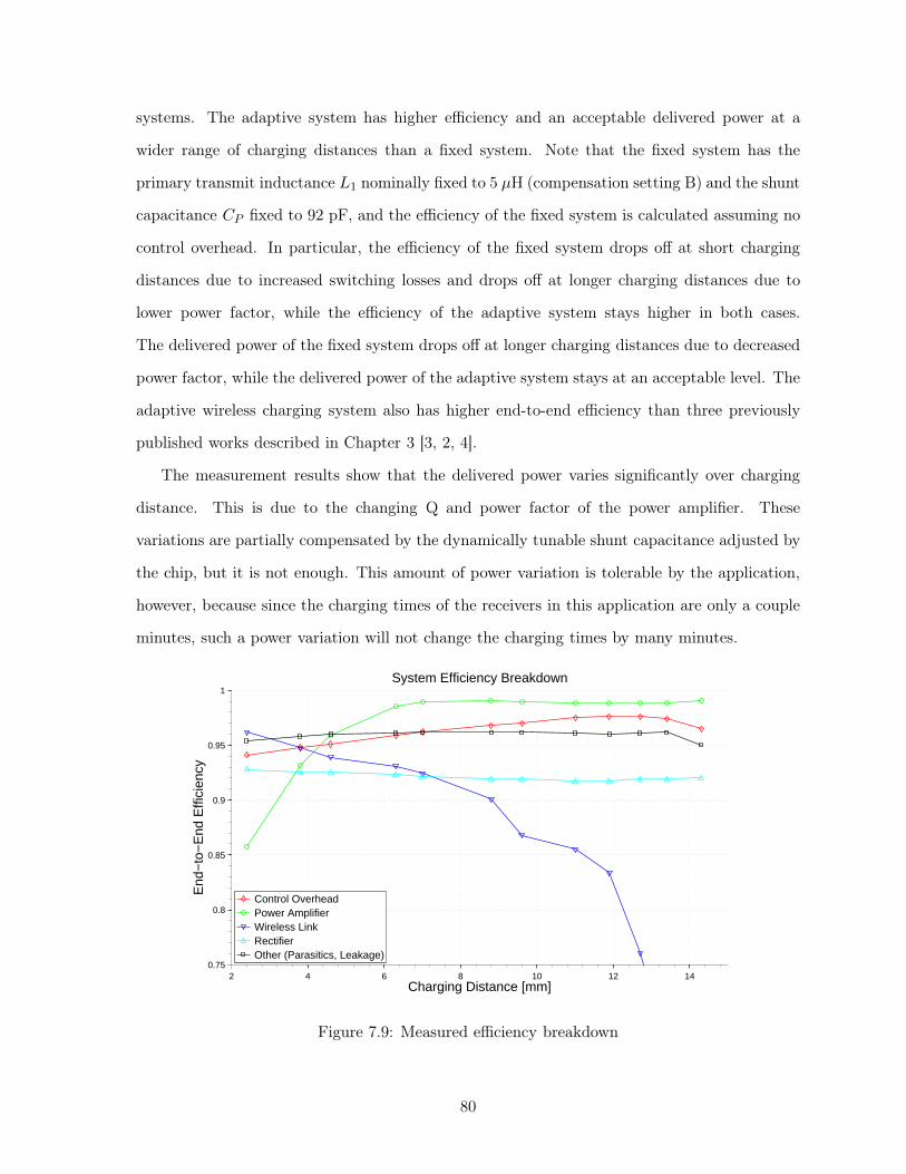
systems. The adaptive system has higher efficiency and an acceptable delivered power at a
wider range of charging distances than a fixed system. Note that the fixed system has the
primary transmit inductance L1 nominally fixed to 5 µH (compensation setting B) and the shunt
capacitance CP fixed to 92 pF, and the efficiency of the fixed system is calculated assuming no
control overhead. In particular, the efficiency of the fixed system drops off at short charging
distances due to increased switching losses and drops off at longer charging distances due to
lower power factor, while the efficiency of the adaptive system stays higher in both cases.
The delivered power of the fixed system drops off at longer charging distances due to decreased
power factor, while the delivered power of the adaptive system stays at an acceptable level. The
adaptive wireless charging system also has higher end-to-end efficiency than three previously
published works described in Chapter 3 [3, 2, 4].
The measurement results show that the delivered power varies significantly over charging
distance. This is due to the changing Q and power factor of the power amplifier. These
variations are partially compensated by the dynamically tunable shunt capacitance adjusted by
the chip, but it is not enough. This amount of power variation is tolerable by the application,
however, because since the charging times of the receivers in this application are only a couple
minutes, such a power variation will not change the charging times by many minutes.
2 4 6 8 10 12 140.75
0.8
0.85
0.9
0.95
1
Charging Distance [mm]
End
−to
−E
nd E
ffici
ency
System Efficiency Breakdown
Control Overhead Power Amplifier Wireless Link Rectifier Other (Parasitics, Leakage)
Figure 7.9: Measured efficiency breakdown
80
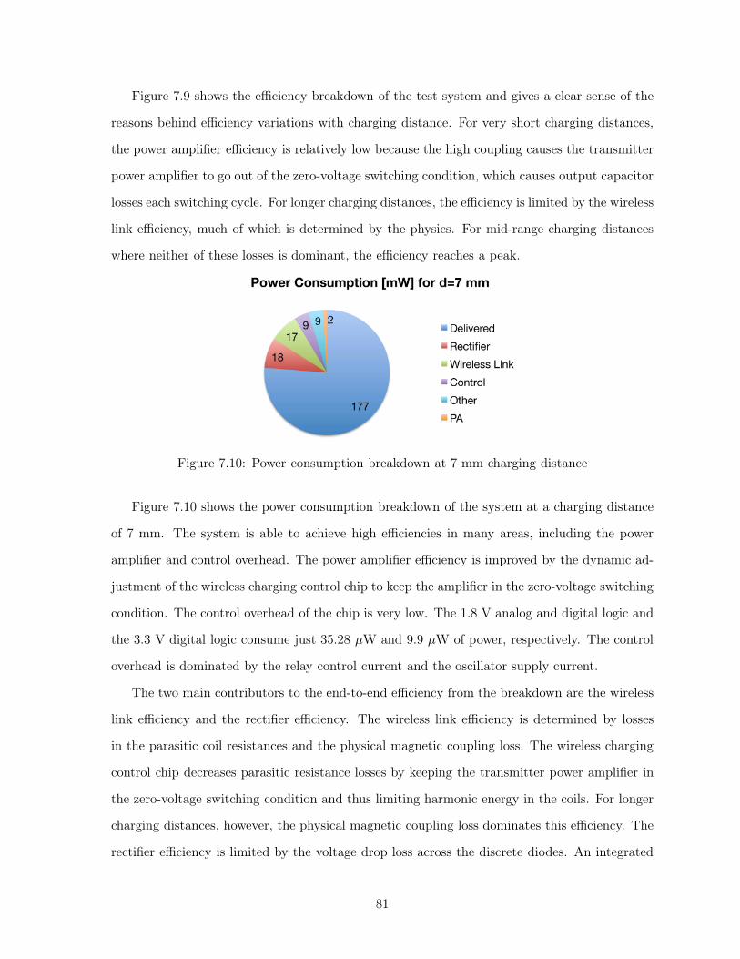
Figure 7.9 shows the efficiency breakdown of the test system and gives a clear sense of the
reasons behind efficiency variations with charging distance. For very short charging distances,
the power amplifier efficiency is relatively low because the high coupling causes the transmitter
power amplifier to go out of the zero-voltage switching condition, which causes output capacitor
losses each switching cycle. For longer charging distances, the efficiency is limited by the wireless
link efficiency, much of which is determined by the physics. For mid-range charging distances
where neither of these losses is dominant, the efficiency reaches a peak.
Figure 7.10: Power consumption breakdown at 7 mm charging distance
Figure 7.10 shows the power consumption breakdown of the system at a charging distance
of 7 mm. The system is able to achieve high efficiencies in many areas, including the power
amplifier and control overhead. The power amplifier efficiency is improved by the dynamic ad-
justment of the wireless charging control chip to keep the amplifier in the zero-voltage switching
condition. The control overhead of the chip is very low. The 1.8 V analog and digital logic and
the 3.3 V digital logic consume just 35.28 µW and 9.9 µW of power, respectively. The control
overhead is dominated by the relay control current and the oscillator supply current.
The two main contributors to the end-to-end efficiency from the breakdown are the wireless
link efficiency and the rectifier efficiency. The wireless link efficiency is determined by losses
in the parasitic coil resistances and the physical magnetic coupling loss. The wireless charging
control chip decreases parasitic resistance losses by keeping the transmitter power amplifier in
the zero-voltage switching condition and thus limiting harmonic energy in the coils. For longer
charging distances, however, the physical magnetic coupling loss dominates this efficiency. The
rectifier efficiency is limited by the voltage drop loss across the discrete diodes. An integrated
81

CMOS rectifier would increase this efficiency.
7.5 Comparison to Previous Work
Figure 7.11: Specification comparison to previous published work and commercial products
Figure 7.11 compares critical specifications of this work to previously published work and com-
mercial products currently available [34, 1, 3, 4, 2, 35, 36, 12, 37, 13]. In the academic arena,
many other publications have demonstrated wireless power systems for medical applications,
such as deep-brain or retinal stimulation. These systems are all based on resonant inductive
power transfer like in this work, and all use similarly sized coils to transfer similar power levels
over similar distances.
There are two main differences between this work and previously published academic work.
The first is that previous systems are designed for a constant output voltage. This implies
an application in which the transmitter is continuously supplying a receiver device with power
to maintain a supply voltage in the receiver. In contrast, this work is designed for a variable
output voltage. This imposes more variability on the transmitter-side loading. This is also
82

more suitable for the application of portable-to-portable wireless charging, in which it is more
convenient for the user to quickly charge a portable device for a long battery life as opposed to
constantly wirelessly powering this portable device.
The second difference is in the measured end-to-end efficiency of this system versus previous
systems. The peak efficiency is higher than previous work, and the efficiency is higher over a
range of charging distances. This is due to the demonstrated power amplifier control loop as
well as the system design, and it has advantages for the portable-to-portable wireless charging
application in which the transmitter is energy-constrained and efficiency is key.
In the industrial arena, many products and standards exist with similar specifications com-
pared with this work. These standards all support resonant inductive transfer of wireless power
over similar distances. The major difference is the application. Consumer products on the mar-
ket today focus on pad-based charging of higher-power consumer electronics such as cell phones.
This means these products have larger coils and transfer higher power. This work focuses on
the application of charging lower-power consumer electronics devices from higher-power ones.
As a result, the system designed in this work has smaller coils and lower power. This new ap-
plication space is largely unexplored by industry and has potential because of the vast number
of low-power portable devices people own and because of the ubiquity of cell phones to charge
these portable devices.
In summary, the unique design of the system in this work allows the system to achieve
high efficiency in the dynamically changing conditions of portable-to-portable wireless charging,
which is a key enabler. This promising application is currently underdeveloped in industry.
7.6 Prototype System Implementation
A prototype system is designed and implemented that draws energy from a cell phone battery
to wirelessly charge low-power portable devices. The design of this prototype system focuses
on a small form factor and high charging efficiency.
83
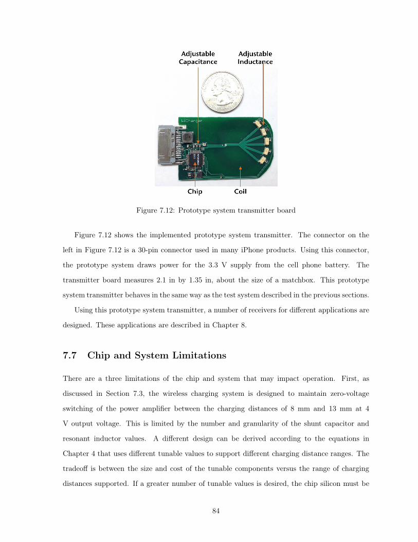
Figure 7.12: Prototype system transmitter board
Figure 7.12 shows the implemented prototype system transmitter. The connector on the
left in Figure 7.12 is a 30-pin connector used in many iPhone products. Using this connector,
the prototype system draws power for the 3.3 V supply from the cell phone battery. The
transmitter board measures 2.1 in by 1.35 in, about the size of a matchbox. This prototype
system transmitter behaves in the same way as the test system described in the previous sections.
Using this prototype system transmitter, a number of receivers for different applications are
designed. These applications are described in Chapter 8.
7.7 Chip and System Limitations
There are a three limitations of the chip and system that may impact operation. First, as
discussed in Section 7.3, the wireless charging system is designed to maintain zero-voltage
switching of the power amplifier between the charging distances of 8 mm and 13 mm at 4
V output voltage. This is limited by the number and granularity of the shunt capacitor and
resonant inductor values. A different design can be derived according to the equations in
Chapter 4 that uses different tunable values to support different charging distance ranges. The
tradeoff is between the size and cost of the tunable components versus the range of charging
distances supported. If a greater number of tunable values is desired, the chip silicon must be
84
redesigned to incorporate more compensation settings (more than the current number of five).
Also, ideally, care should be taken to not vary the tunable components too much between
consecutive settings. If consecutive settings are very different values of the tunable components,
then for certain charging conditions the chip may not be able to determine a satisfactory setting
with respect to the switch turn-on voltage being within the specified range (set by 0 and V REF
at the analog block of the chip). In this case, the chip will oscillate between two consecutive
settings. This is not ideal but entirely acceptable, since it has little effect on the operation or
efficiency of the wireless charging system (beyond the small efficiency loss due to the outputs
that switch at the ∼ 1 kHz control logic clock frequency). V REF may be increased to increase
this range and prevent such oscillations, at the cost of decreased control on the switch turn-
on voltage values that are considered satisfactory by the chip. V REF must not be increased
beyond 3.3 V, which is the voltage rating of the corresponding input transistor in the analog
block.
A second limitation relates to chip operation as the load and coupling conditions are varied
very slowly. When the switch turn-on voltage is very close to the endpoints of the specified
range (0 or V REF ), the comparators in the analog block of the chip have significantly longer
decision times. In some cases, this delay may be longer than the delay before the comparator
outputs are clocked into the logic in the digital block of the chip. The result of this is that
two comparator outputs may be high, and two consecutive settings may be chosen by the chip
at the same time. After this, as the chip performs further compensation, these two settings
are adjusted independently. The presence of multiple settings is eliminated when an extreme
setting is chosen by the chip (Z or D) or on reset. The presence of multiple settings has
only a small effect on the wireless charging system operation. The setting with a larger shunt
capacitance and smaller resonant inductance dominates the system operation, and any other
selected settings have little effect. The efficiency is degraded slightly due mostly to the power
dissipation of additional relay control currents. For every additional relay that turns on, there
is an additional 1.7 mA of control current from a 1.8 V supply. This corresponds to 1.7×1.8 ≈ 3
mW of additional power dissipation, or 1.5% of the nominal 200 mW delivered power.
A third limitation relates to system operation at power-on, especially when there is no
receiver present. In all cases, the chip starts at the lowest compensation setting Z at power-on,
85
and in the case with no receiver, the chip quickly increases the setting to A, then B, then C,
then D. As the settings are switched, one relay for the transmitter multi-tapped coil must turn
off and another must turn on. The relays are designed such that the turn-on time is much
shorter than the turn-off time. If the 1.8 V supply for the relay control currents is unstable
during this time, however, such as at power-on, the relays may take an unusually long time to
turn-on. If the turn-on time exceeds the turn-off time, the current flowing through the resonant
tank will have no path to flow, and this will cause the current to go completely out of sync with
the power amplifier switch driving this current. The result is very limited power transfer at
poor efficiency. This problem is especially prevalent when hot-plugging a prototype system into
a cell phone. Although this is a serious problem, it is an easy one to solve as long as the 1.8 V
supply rail is allowed to stabilize for a sufficient amount of time (a couple milliseconds) before
the power amplifier switch starts switching at power-on, and as long as the relay control circuits
are carefully designed such that the turn-on time is much shorter than the turn-off time.
7.8 Summary of Wireless Charging Integrated Circuit and Sys-
tem Design and Implementation
The last three chapters present a complete wireless charging system design and implementation
consisting of a resonant inductive wireless power circuit with dynamic adjustment of the primary
side controlled by an ultra low-power microchip. All discrete components in the system are
chosen or designed carefully for maximum efficiency. The system achieves higher end-to-end
efficiency than previously published results over varying charging conditions. The next chapter
highlights some of the applications of this system in practice.
86
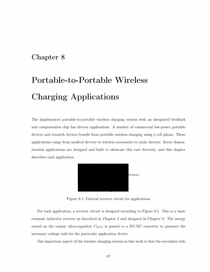
Chapter 8
Portable-to-Portable Wireless
Charging Applications
The implemented portable-to-portable wireless charging system with an integrated feedback
and compensation chip has diverse applications. A number of commercial low-power portable
devices and research devices benefit from portable wireless charging using a cell phone. These
applications range from medical devices to wireless accessories to niche devices. Seven demon-
stration applications are designed and built to showcase this vast diversity, and this chapter
describes each application.
L2
C2
COUT
DC-DC To Device
Figure 8.1: General receiver circuit for applications
For each application, a receiver circuit is designed according to Figure 8.1. This is a basic
resonant inductive receiver as described in Chapter 2 and designed in Chapter 6. The energy
stored on the output ultra-capacitor COUT is passed to a DC-DC converter to generate the
necessary voltage rails for the particular application device.
One important aspect of the wireless charging system in this work is that the secondary-side
87
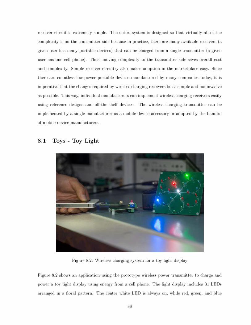
receiver circuit is extremely simple. The entire system is designed so that virtually all of the
complexity is on the transmitter side because in practice, there are many available receivers (a
given user has many portable devices) that can be charged from a single transmitter (a given
user has one cell phone). Thus, moving complexity to the transmitter side saves overall cost
and complexity. Simple receiver circuitry also makes adoption in the marketplace easy. Since
there are countless low-power portable devices manufactured by many companies today, it is
imperative that the changes required by wireless charging receivers be as simple and noninvasive
as possible. This way, individual manufacturers can implement wireless charging receivers easily
using reference designs and off-the-shelf devices. The wireless charging transmitter can be
implemented by a single manufacturer as a mobile device accessory or adopted by the handful
of mobile device manufacturers.
8.1 Toys - Toy Light
Figure 8.2: Wireless charging system for a toy light display
Figure 8.2 shows an application using the prototype wireless power transmitter to charge and
power a toy light display using energy from a cell phone. The light display includes 31 LEDs
arranged in a floral pattern. The center white LED is always on, while red, green, and blue
88
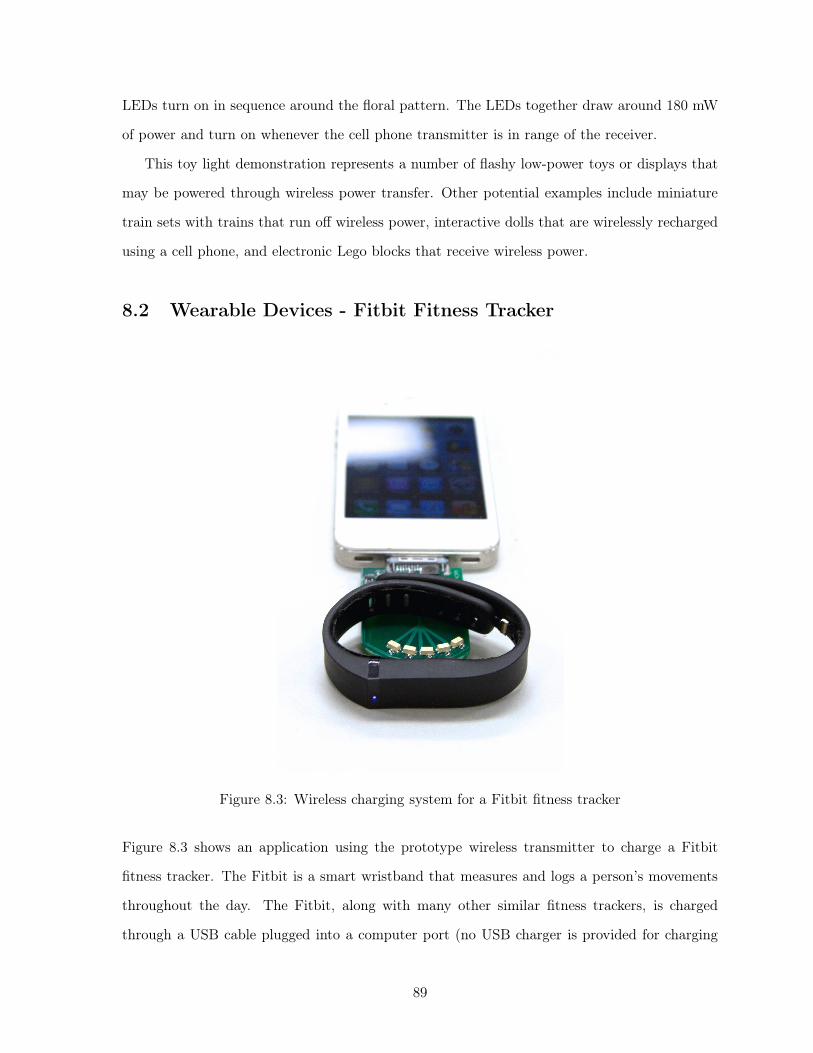
LEDs turn on in sequence around the floral pattern. The LEDs together draw around 180 mW
of power and turn on whenever the cell phone transmitter is in range of the receiver.
This toy light demonstration represents a number of flashy low-power toys or displays that
may be powered through wireless power transfer. Other potential examples include miniature
train sets with trains that run off wireless power, interactive dolls that are wirelessly recharged
using a cell phone, and electronic Lego blocks that receive wireless power.
8.2 Wearable Devices - Fitbit Fitness Tracker
Figure 8.3: Wireless charging system for a Fitbit fitness tracker
Figure 8.3 shows an application using the prototype wireless transmitter to charge a Fitbit
fitness tracker. The Fitbit is a smart wristband that measures and logs a person’s movements
throughout the day. The Fitbit, along with many other similar fitness trackers, is charged
through a USB cable plugged into a computer port (no USB charger is provided for charging
89
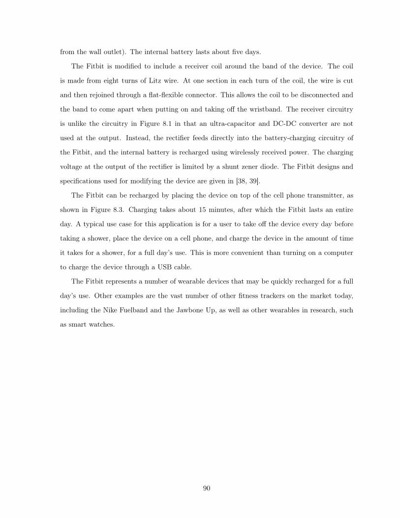
from the wall outlet). The internal battery lasts about five days.
The Fitbit is modified to include a receiver coil around the band of the device. The coil
is made from eight turns of Litz wire. At one section in each turn of the coil, the wire is cut
and then rejoined through a flat-flexible connector. This allows the coil to be disconnected and
the band to come apart when putting on and taking off the wristband. The receiver circuitry
is unlike the circuitry in Figure 8.1 in that an ultra-capacitor and DC-DC converter are not
used at the output. Instead, the rectifier feeds directly into the battery-charging circuitry of
the Fitbit, and the internal battery is recharged using wirelessly received power. The charging
voltage at the output of the rectifier is limited by a shunt zener diode. The Fitbit designs and
specifications used for modifying the device are given in [38, 39].
The Fitbit can be recharged by placing the device on top of the cell phone transmitter, as
shown in Figure 8.3. Charging takes about 15 minutes, after which the Fitbit lasts an entire
day. A typical use case for this application is for a user to take off the device every day before
taking a shower, place the device on a cell phone, and charge the device in the amount of time
it takes for a shower, for a full day’s use. This is more convenient than turning on a computer
to charge the device through a USB cable.
The Fitbit represents a number of wearable devices that may be quickly recharged for a full
day’s use. Other examples are the vast number of other fitness trackers on the market today,
including the Nike Fuelband and the Jawbone Up, as well as other wearables in research, such
as smart watches.
90
8.3 Medical Devices - Cochlear Implant
Figure 8.4: Wireless charging receiver for a cochlear implant
Figure 8.4 shows the wireless charging receiver for a research cochlear implant. A cochlear
implant is a medical device that is surgically implanted inside the ear with electrodes to stimulate
neurons in the cochlea to give the sensation of hearing. The chip on the top of the board in
the figure is a sound processor that converts input sound to the stimulation waveforms for the
electrodes. The chip is designed for a fully-implantable cochlear implant prototype in which
there are no devices external to the ear and the entire implant is invisible from the perspective
of another person. The detailed design for the chip is reported in [40]. All other components
required for operation of the cochlear implant are on the board, including the wireless power
receiver, power converters, and clock generators. The entire system is the same size as a
conventional cochlear implant.
Wireless power is crucial for implanted devices such as the cochlear implant. The wireless
power receiver is located on the bottom of the board in the figure. The basic receiver circuit in
Figure 8.1 is used with DC-DC converters to generate 0.6 V, 1.5 V, 3.3 V, and 8.2 V supplies
for the chip. The entire system can be charged in about 2 minutes (to charge a 1.5 F ultra-
capacitor) for a 7.5-hour battery life. This is convenient for users, since only a couple quick
charge sessions using a cell phone are needed per day.
The cochlear implant is a representative of a number of medical devices, implanted and
91
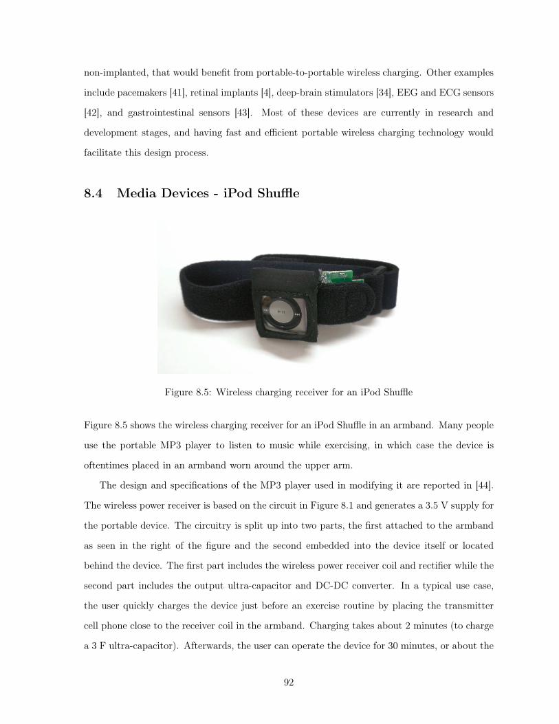
non-implanted, that would benefit from portable-to-portable wireless charging. Other examples
include pacemakers [41], retinal implants [4], deep-brain stimulators [34], EEG and ECG sensors
[42], and gastrointestinal sensors [43]. Most of these devices are currently in research and
development stages, and having fast and efficient portable wireless charging technology would
facilitate this design process.
8.4 Media Devices - iPod Shuffle
Figure 8.5: Wireless charging receiver for an iPod Shuffle
Figure 8.5 shows the wireless charging receiver for an iPod Shuffle in an armband. Many people
use the portable MP3 player to listen to music while exercising, in which case the device is
oftentimes placed in an armband worn around the upper arm.
The design and specifications of the MP3 player used in modifying it are reported in [44].
The wireless power receiver is based on the circuit in Figure 8.1 and generates a 3.5 V supply for
the portable device. The circuitry is split up into two parts, the first attached to the armband
as seen in the right of the figure and the second embedded into the device itself or located
behind the device. The first part includes the wireless power receiver coil and rectifier while the
second part includes the output ultra-capacitor and DC-DC converter. In a typical use case,
the user quickly charges the device just before an exercise routine by placing the transmitter
cell phone close to the receiver coil in the armband. Charging takes about 2 minutes (to charge
a 3 F ultra-capacitor). Afterwards, the user can operate the device for 30 minutes, or about the
92
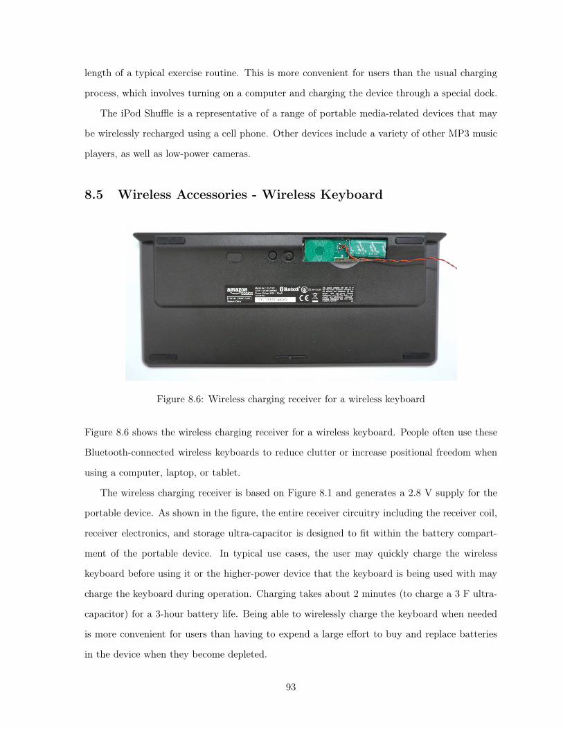
length of a typical exercise routine. This is more convenient for users than the usual charging
process, which involves turning on a computer and charging the device through a special dock.
The iPod Shuffle is a representative of a range of portable media-related devices that may
be wirelessly recharged using a cell phone. Other devices include a variety of other MP3 music
players, as well as low-power cameras.
8.5 Wireless Accessories - Wireless Keyboard
Figure 8.6: Wireless charging receiver for a wireless keyboard
Figure 8.6 shows the wireless charging receiver for a wireless keyboard. People often use these
Bluetooth-connected wireless keyboards to reduce clutter or increase positional freedom when
using a computer, laptop, or tablet.
The wireless charging receiver is based on Figure 8.1 and generates a 2.8 V supply for the
portable device. As shown in the figure, the entire receiver circuitry including the receiver coil,
receiver electronics, and storage ultra-capacitor is designed to fit within the battery compart-
ment of the portable device. In typical use cases, the user may quickly charge the wireless
keyboard before using it or the higher-power device that the keyboard is being used with may
charge the keyboard during operation. Charging takes about 2 minutes (to charge a 3 F ultra-
capacitor) for a 3-hour battery life. Being able to wirelessly charge the keyboard when needed
is more convenient for users than having to expend a large effort to buy and replace batteries
in the device when they become depleted.
93
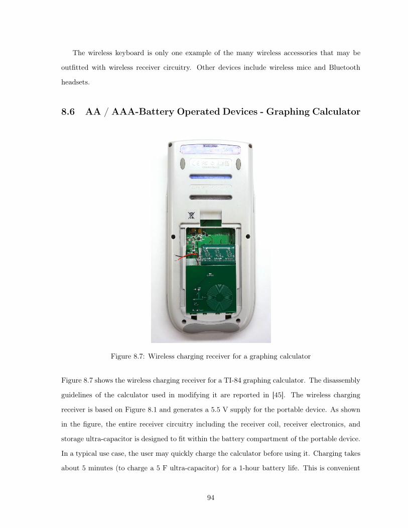
The wireless keyboard is only one example of the many wireless accessories that may be
outfitted with wireless receiver circuitry. Other devices include wireless mice and Bluetooth
headsets.
8.6 AA / AAA-Battery Operated Devices - Graphing Calculator
Figure 8.7: Wireless charging receiver for a graphing calculator
Figure 8.7 shows the wireless charging receiver for a TI-84 graphing calculator. The disassembly
guidelines of the calculator used in modifying it are reported in [45]. The wireless charging
receiver is based on Figure 8.1 and generates a 5.5 V supply for the portable device. As shown
in the figure, the entire receiver circuitry including the receiver coil, receiver electronics, and
storage ultra-capacitor is designed to fit within the battery compartment of the portable device.
In a typical use case, the user may quickly charge the calculator before using it. Charging takes
about 5 minutes (to charge a 5 F ultra-capacitor) for a 1-hour battery life. This is convenient
94
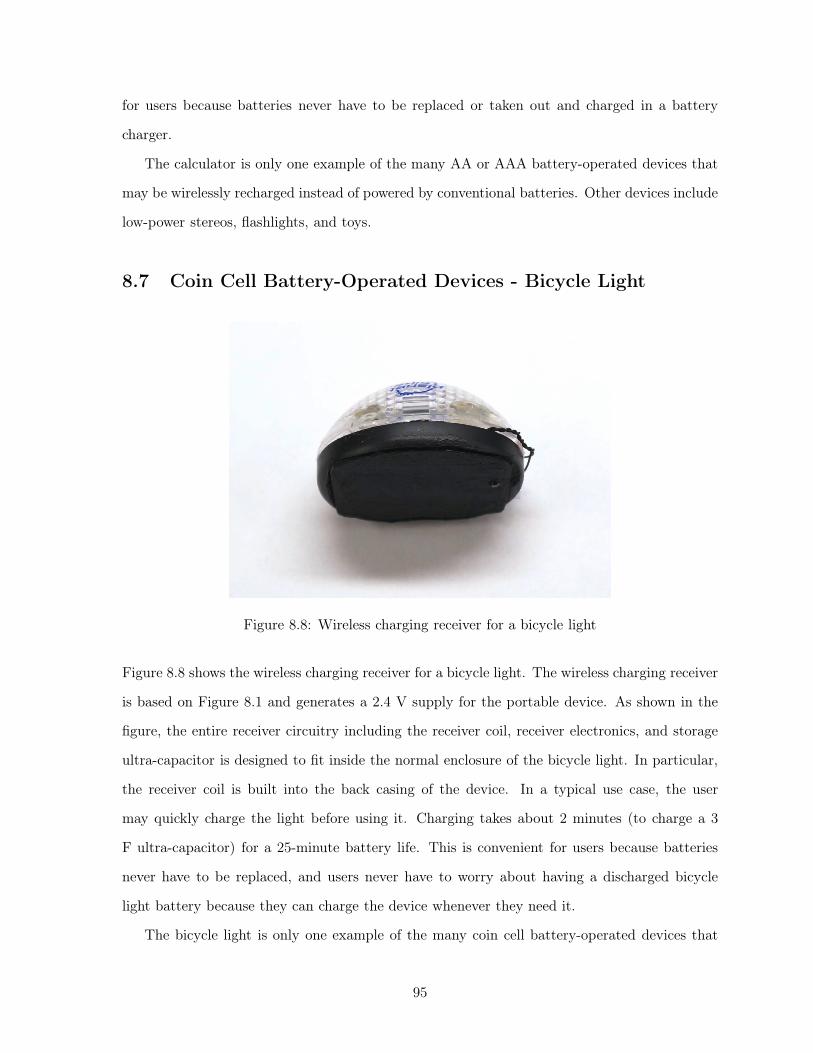
for users because batteries never have to be replaced or taken out and charged in a battery
charger.
The calculator is only one example of the many AA or AAA battery-operated devices that
may be wirelessly recharged instead of powered by conventional batteries. Other devices include
low-power stereos, flashlights, and toys.
8.7 Coin Cell Battery-Operated Devices - Bicycle Light
Figure 8.8: Wireless charging receiver for a bicycle light
Figure 8.8 shows the wireless charging receiver for a bicycle light. The wireless charging receiver
is based on Figure 8.1 and generates a 2.4 V supply for the portable device. As shown in the
figure, the entire receiver circuitry including the receiver coil, receiver electronics, and storage
ultra-capacitor is designed to fit inside the normal enclosure of the bicycle light. In particular,
the receiver coil is built into the back casing of the device. In a typical use case, the user
may quickly charge the light before using it. Charging takes about 2 minutes (to charge a 3
F ultra-capacitor) for a 25-minute battery life. This is convenient for users because batteries
never have to be replaced, and users never have to worry about having a discharged bicycle
light battery because they can charge the device whenever they need it.
The bicycle light is only one example of the many coin cell battery-operated devices that
95

may be wirelessly recharged instead of powered by conventional batteries. Other devices include
watches, hearing aids, and toys.
8.8 Chapter Summary
Category Device Charging Time Usage Time
Toys Toy Light N/A N/A
Wearable Devices Fitbit Fitness Tracker 15 Minutes 1 Day
Medical Devices Cochlear Implant 2 Minutes 7.5 Hours
Media Devices iPod Shuffle 2 Minutes 30 Minutes
Wireless Accessories Wireless Keyboard 2 Minutes 3 Hours
AA / AAA Battery Devices Graphing Calculator 5 Minutes 1 Hour
Coin Cell Battery Devices Bicycle Light 2 Minutes 25 Minutes
Table 8.1: Summary of wireless charging receiver applications
Table 8.1 shows a summary of the diverse applications for the portable-to-portable wireless
charging system. This shows the vast number of portable devices that would benefit from this
system, in many different areas. In all cases, a person can charge a portable device using a cell
phone in a few minutes and subsequently use the device for a typical day. Note that as portable
devices are developed to use less power, these devices will be able to be charged in a shorter
amount of time and last on that charge for a longer amount of time.
96

Chapter 9
Conclusions and Future Directions
9.1 Summary of Contributions
Today’s world is dominated by portable electronics. These devices facilitate people’s activities
in a number of areas, from entertainment to health to work. Many of the ways low-power
portable devices influence people’s lives are highlighted in Chapter 8. In addition, researchers
and companies are actively exploring new portable devices, in particular devices that integrate
more functions and devices that sense more of the world around us.
The fundamental requirement of all electronics is the supply of power. With the pervasive-
ness of low-power portable devices, the question of how to supply the unique power demands
of each device is becoming an escalating issue. Most portables on the market today answer this
question through wired charging cables. But as the number of portable devices increases further,
increasing the number of charging cables in proportion will lead to greater user inconvenience,
increased costs, and decreased environmental sustainability.
This work attempts to solve this issue by proposing a common wireless power interface
to recharge all these low-power portable devices using higher-power portable devices. Higher-
power portable devices such as cell phones are ubiquitous today and are excellent sources of
portable energy. Since many portable devices people use are generally closer to people’s cell
phones than to electrical outlets, in many cases it is more convenient to recharge these portable
devices using cell phones than using wired chargers. The use case model of quick wireless
charging of portable devices on demand is an attractive one in many applications, as outlined
97
in Chapter 8. A common wireless charging interface also avoids the issue of the number of
charging cables scaling in proportion with the number of portable devices, and this facilitates
increased environmental sustainability and lower cost.
The portable-to-portable wireless charging system designed in this work attempts to solve
many of the challenges associated with portable wireless power transfer. These challenges
stem from the use case model, in which the transmitter portable device is by definition energy
constrained and the charging process naturally entails dynamically changing coupling and load
conditions. This means that maintaining high efficiency while delivering consistent power levels
over changing conditions is key. This work addresses these challenges through derivation of
a new power amplifier control technique, a complete wireless charging integrated circuit and
system design, and a series of demonstration applications.
Mathematical analysis presented in Chapters 2-4 develops the theory behind the standard
wireless power topology and shows how this design reacts to changing conditions with respect
to key metrics. A power amplifier control method is derived that improves upon the standard
wireless power topology to improve efficiency and balance power as coupling and load conditions
change. Specifically, the control loop includes feedback from the transmitter-side power amplifier
to inform compensation of the power amplifier shunt capacitance and primary resonant tank
inductance to maintain zero-voltage switching while regulating power.
Integrated circuit and system design presented in Chapters 5-7 implement the power am-
plifier control loop in an adaptive resonant inductive wireless charging system. A microchip is
fabricated in a 0.18 µm HVCMOS process that dynamically compensates the power amplifier
based on changing conditions. A complete wireless charging system is built around this mi-
crochip to wirelessly transfer energy from a cell phone battery to a low-power portable device.
A maximum end-to-end efficiency of 78% is achieved transferring about 200 mW over a 7 mm
distance between 25-30 mm diameter coils. Efficiencies over 70% are maintained for a range of
distances from 4-12 mm and delivered power levels vary less than 40% for a range of distances
from 7-12 mm.
As detailed in Chapter 8, seven demonstration applications are designed and implemented
that showcase the applicability of the portable-to-portable wireless charging system to recharge a
diverse set of portable devices, from wearable devices to medical implants to wireless accessories.
98
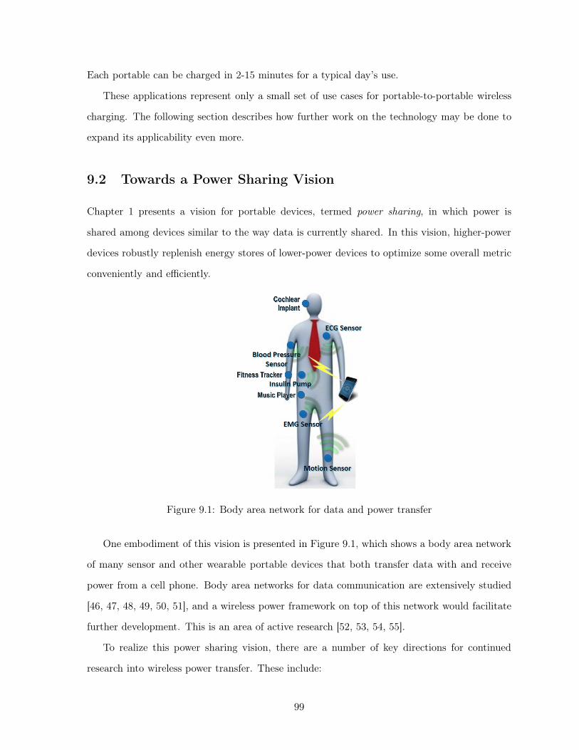
Each portable can be charged in 2-15 minutes for a typical day’s use.
These applications represent only a small set of use cases for portable-to-portable wireless
charging. The following section describes how further work on the technology may be done to
expand its applicability even more.
9.2 Towards a Power Sharing Vision
Chapter 1 presents a vision for portable devices, termed power sharing, in which power is
shared among devices similar to the way data is currently shared. In this vision, higher-power
devices robustly replenish energy stores of lower-power devices to optimize some overall metric
conveniently and efficiently.
Figure 9.1: Body area network for data and power transfer
One embodiment of this vision is presented in Figure 9.1, which shows a body area network
of many sensor and other wearable portable devices that both transfer data with and receive
power from a cell phone. Body area networks for data communication are extensively studied
[46, 47, 48, 49, 50, 51], and a wireless power framework on top of this network would facilitate
further development. This is an area of active research [52, 53, 54, 55].
To realize this power sharing vision, there are a number of key directions for continued
research into wireless power transfer. These include:
99
• Power transfer over longer distances: A major technology required by the power
sharing vision is the ability to wirelessly transmit energy over longer distances, on the
order of a meter. The main impediment to achieving this is the extremely low coupling
between a transmitter and receiver separated by a long distance. This leads to system
issues such as low end-to-end efficiency, as explored in [56, 57]. A number of potential
research avenues exist to overcome this obstacle, however, and systems exist that transfer
power over longer distances [58]. First, low efficiency may be tolerable in some applications
with low or non-critical power requirements. Second, different transmitter/receiver designs
or frequencies can be investigated to decrease the effect of low coupling [59, 60, 24, 61].
Third, intermediate or relay nodes may be added to a wireless power system to decrease
the effective coupling distance [11].
• Power transfer among multiple devices: A number of considerations arise with
power transfer among multiple devices as compared to power transfer between a single
transmitter and a single receiver. These include the differing power sourcing and sink-
ing specifications of each device, the differing amounts of energy stored in each device,
the differing coupling and load conditions present between each pair of devices, and the
methods and fairness of these methods of transferring power from a single transmitter
to multiple receivers or from multiple transmitters to a single receiver. Some of these
considerations are included in [62, 63]. Metrics can be defined that consider the overall
performance of the power network with respect to efficiency or charging time, and systems
can be designed that achieve an overall optimum.
• User interaction with wireless power transfer: As the number of wireless power-
enabled devices increases, an interesting question arises regarding exactly what involve-
ment users should have with the sharing of energy among devices. In current wired
charging use case models and in the wireless charging use case model proposed in this
work, the user consciously enables the transfer of energy from a transmitter to receiver.
In the future, a better use case model might be automatic transfer of energy, in which
many devices stay charged without any user effort. Other issues worth considering are
which devices are allowed to share power, and how this is determined on the device level
100
and on the user level.
• Security with wireless power transfer: As with any technology in which operation
uses a public medium, power transfer over the air is by default vulnerable to security
breaches. Possible problems include undesired transfer of energy from a user device to an
unapproved device, which raises issues with user satisfaction, and transfer of an undesir-
ably high amount of power from a user device, which raises issues with user safety. Security
layers need to be designed over the power electronics to authenticate users and protect
against adversaries. Security is well explored in the field of wireless data communication
[64, 65] and these principles can be applied to wireless power transfer.
• Multi-modal operation with energy harvesting: As portable devices are developed
with lower and lower power requirements, energy harvesting becomes viable for the energy
requirements of more devices, at least in certain modes of operation [66]. Certain applica-
tions can benefit from energy harvesting when power demands are low and wireless power
transfer when power demands are high. Devices with energy harvesting mechanisms can
also self-replenish their stores of energy to transfer to other devices [67].
101
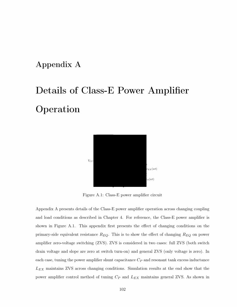
Appendix A
Details of Class-E Power Amplifier
Operation
−VCC
+
LCHOKE
IO
v(wt)
iS
q(t)
iC
CP
iR
CR
LR
LEX
+
vEX(wt)
−
RPRI +REQ
+
vS(wt)
−
Figure A.1: Class-E power amplifier circuit
Appendix A presents details of the Class-E power amplifier operation across changing coupling
and load conditions as described in Chapter 4. For reference, the Class-E power amplifier is
shown in Figure A.1. This appendix first presents the effect of changing conditions on the
primary-side equivalent resistance REQ. This is to show the effect of changing REQ on power
amplifier zero-voltage switching (ZVS). ZVS is considered in two cases: full ZVS (both switch
drain voltage and slope are zero at switch turn-on) and general ZVS (only voltage is zero). In
each case, tuning the power amplifier shunt capacitance CP and resonant tank excess inductance
LEX maintains ZVS across changing conditions. Simulation results at the end show that the
power amplifier control method of tuning CP and LEX maintains general ZVS. As shown in
102

Chapter 4, this improves efficiency and balances delivered power across changing conditions.
A.1 Effect of Changing Coupling and Output Voltage on Equiv-
alent Resistance
The effect of changing coupling and output voltage on primary-side equivalent resistance is
found by considering the output power.
From Subsection 2.3.1, the output power is delivered only by the component of the rectifier
voltage that is at the operating frequency. This component has amplitude 4πVOUT . Thus, the
average output power is
POUT =1
2
(
4
π
)2 V 2OUT
RL(A.1.1)
From Equation 2.3.3, the output power may also be written as
POUT = V 2S,rms
(
k2L1C2RL
(k2L1 + C2RPRI(RL +R2))2
)
(A.1.2)
Equating the two expressions and solving for RL gives
V 2S,rms
(
k2L1C2RL
(k2L1 + C2RPRI(RL +R2))2
)
=1
2
(
4
π
)2 V 2OUT
RL(A.1.3)
⇒√
V 2S
(
k2L1C2RL
(k2L1 + C2RPRI(RL +R2))2
)
=
√
(
4
π
)2 V 2OUT
RL(A.1.4)
⇒ RL =
4πVOUT
|VS |(
k2L1 + C2RPRIR2
)
k√L1C2 − C2RPRI
4πVOUT
|VS |(A.1.5)
⇒ RL =k2L1L2w
2 +R2RPRI
k√L1L2w
π4
|VS |VOUT
−RPRI
(A.1.6)
where the last equation comes from the fact that w = 1√L2C2
.
Then from Equation 2.3.2, the reflected primary-side impedance at resonance is
REQ =k2L1
C2(R2 +RL)(A.1.7)
103
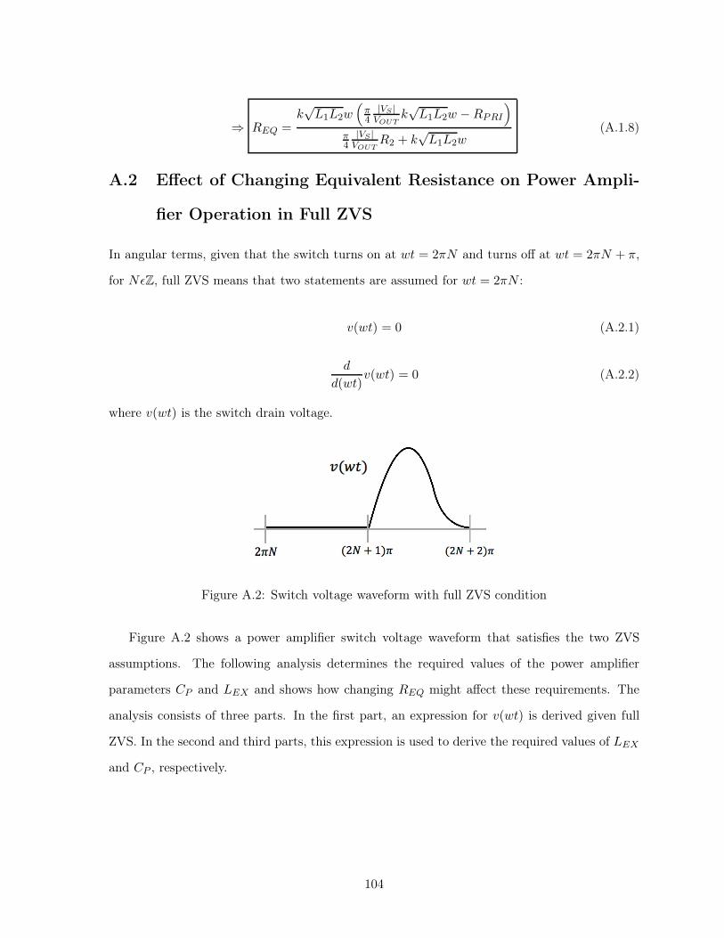
⇒ REQ =k√L1L2w
(
π4
|VS |VOUT
k√L1L2w −RPRI
)
π4
|VS |VOUT
R2 + k√L1L2w
(A.1.8)
A.2 Effect of Changing Equivalent Resistance on Power Ampli-
fier Operation in Full ZVS
In angular terms, given that the switch turns on at wt = 2πN and turns off at wt = 2πN + π,
for NǫZ, full ZVS means that two statements are assumed for wt = 2πN :
v(wt) = 0 (A.2.1)
d
d(wt)v(wt) = 0 (A.2.2)
where v(wt) is the switch drain voltage.
Figure A.2: Switch voltage waveform with full ZVS condition
Figure A.2 shows a power amplifier switch voltage waveform that satisfies the two ZVS
assumptions. The following analysis determines the required values of the power amplifier
parameters CP and LEX and shows how changing REQ might affect these requirements. The
analysis consists of three parts. In the first part, an expression for v(wt) is derived given full
ZVS. In the second and third parts, this expression is used to derive the required values of LEX
and CP , respectively.
104

A.2.1 Derivation of v(wt) in Full ZVS Condition
Due to the ZVS assumptions, at wt = 2π,
iC(2π) = wCPd
d(wt)v(wt)|wt=2π = 0 (A.2.3)
Since the switch has just begun to conduct current at this time,
iS(2π) = IO + iR(2π) = 0 (A.2.4)
Let iR(wt) = IR sin(wt+ φ). Then,
IO = −iR(2π) = −IR sin(2π + φ) = −IR sin(φ) (A.2.5)
For π < wt < 2π, in other words when the switch is off,
iC(wt) = IO + IR sin(wt+ φ) = −IR(sin(φ)− sin(wt+ φ)) (A.2.6)
⇒ v(wt) =1
wCP
wtˆ
π
iC(wt)d(wt) = −IRXP [cos(wt+ φ) + cos(φ) + sin(φ)(wt− π)] (A.2.7)
where XP = 1wCP
. At wt = 2π, v(wt) = 0, so
v(2π) = 2 cos(φ) + π sin(φ) = 0 (A.2.8)
⇒ φ = tan−1(− 2
π) ≈ −32.48 (A.2.9)
⇒ iR(wt) = IR sin(wt− 32.48) (A.2.10)
⇒ v(wt) = IOXP
[
wt− 3π
2− π
2cos(wt)− sin(wt)
]
(A.2.11)
This shows that in ZVS, the resonant current is phase shifted from the switch drive voltage
by φ = −32.48. This is observed in the Class-E power amplifier waveforms in Chapter 2, in
Figure 2.7.
105

A.2.2 Derivation of LEX in Full ZVS Condition
The power delivered to RPRI +REQ comes only from voltage that is in phase with the resonant
current. In particular, considering the frequency components of v(wt) at the fundamental
operating frequency, only the component that is in phase with iR(wt) delivers power to the
load. The out-of-phase component is dropped across the excess inductance LEX . Using a
Fourier series expansion, the in-phase component magnitude is,
VS =1
π
2πˆ
π
v(wt) sin(wt+ φ)d(wt) =1
πIOXP
[
2 sin(φ)− π2
4sin(φ)− π
2cos(φ)
]
(A.2.12)
The out-of-phase component magnitude is,
VEX =1
π
2πˆ
π
v(wt) cos(wt+ φ)d(wt) =1
πIOXP
[
2 cos(φ)− π2
4cos(φ) +
π
2sin(φ)
]
(A.2.13)
Since voltage drops are proportional to impedances,
VEX
VS=
wLEX
RPRI +REQ=
(
2− π2
4
)
cos(φ) + π2 sin(φ)
(
2− π2
4
)
sin(φ)− π2 cos(φ)
=π3
16− π
4≈ 1.152 (A.2.14)
This shows that in ZVS, the excess inductance LEX must be related to the reflected resistance
and primary-side resistance RPRI+REQ by a constant factor. In particular, when REQ changes,
ZVS is not maintained unless LEX is adjusted accordingly. Note that given a value for REQ,
there is a unique value of LEX .
A.2.3 Derivation of CP in Full ZVS Condition
Power enters the system through the choke inductor LCHOKE. Ideally, it should be sized as
large as possible to keep the input current IO as constant as possible. Given this, the choke
106

inductor cannot have any average voltage across it, so v(wt) = VCC , or
VCC =1
2π
2πˆ
π
v(wt)d(wt) =1
πIOXP (A.2.15)
Plugging this into Equation A.2.12 gives,
VS = VCC
[
2 sin(φ)− π2
4sin(φ)− π
2cos(φ)
]
= − 4√π2 + 4
VCC ≈ −1.07VCC (A.2.16)
Since IO = −IR sin(φ) = IR2√
π2+4, plugging this into Equation A.2.15 gives,
VCC =2
π√π2 + 4
IRXP (A.2.17)
Since IR = − VS
RPRI+REQ(the negative sign comes from the direction of the currents in Figure
4.6), plugging this and Equation A.2.16 into the previous equation gives,
VCC =8
π(π2 + 4)
VCC
wCP
1
RPRI +REQ
(A.2.18)
⇒ wCP =8
π(π2 + 4)
1
RPRI +REQ
(A.2.19)
This shows that in ZVS, the capacitance CP must be related to the reflected resistance and
primary-side resistance RPRI + REQ by a constant factor. In particular, when REQ changes,
ZVS is not maintained unless CP is adjusted accordingly. Note that given a value for REQ,
there is a unique value of CP .
A.3 Effect of Changing Equivalent Resistance on Power Ampli-
fier Operation in General ZVS
In a more general case, a partial zero-voltage switching condition can be met in which only one
of the assumptions is true, namely that at switch turn-on, only the switch drain voltage is zero.
107
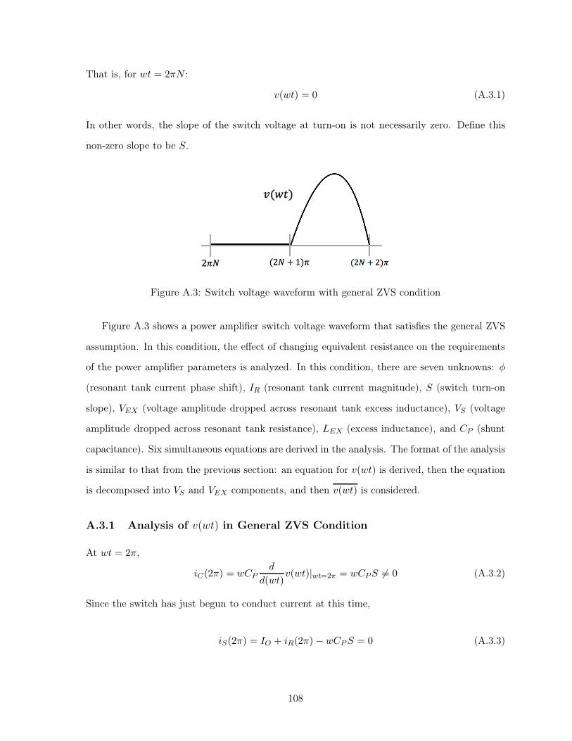
That is, for wt = 2πN :
v(wt) = 0 (A.3.1)
In other words, the slope of the switch voltage at turn-on is not necessarily zero. Define this
non-zero slope to be S.
Figure A.3: Switch voltage waveform with general ZVS condition
Figure A.3 shows a power amplifier switch voltage waveform that satisfies the general ZVS
assumption. In this condition, the effect of changing equivalent resistance on the requirements
of the power amplifier parameters is analyzed. In this condition, there are seven unknowns: φ
(resonant tank current phase shift), IR (resonant tank current magnitude), S (switch turn-on
slope), VEX (voltage amplitude dropped across resonant tank excess inductance), VS (voltage
amplitude dropped across resonant tank resistance), LEX (excess inductance), and CP (shunt
capacitance). Six simultaneous equations are derived in the analysis. The format of the analysis
is similar to that from the previous section: an equation for v(wt) is derived, then the equation
is decomposed into VS and VEX components, and then v(wt) is considered.
A.3.1 Analysis of v(wt) in General ZVS Condition
At wt = 2π,
iC(2π) = wCPd
d(wt)v(wt)|wt=2π = wCPS 6= 0 (A.3.2)
Since the switch has just begun to conduct current at this time,
iS(2π) = IO + iR(2π) −wCPS = 0 (A.3.3)
108

Let iR(wt) = IR sin(wt+ φ). Then,
IO = −iR(2π) + wCPS = −IR sin(2π + φ) + wCPS = −IR sin(φ) + wCPS (A.3.4)
For π < wt < 2π, in other words when the switch is off,
iC(wt) = IO + IR sin(wt+ φ) = −IR(sin(φ)− sin(wt+ φ)) + wCPS (A.3.5)
⇒ v(wt) =1
wCP
wtˆ
π
iC(wt)d(wt) (A.3.6)
⇒ v(wt) = −IRXP [cos(wt+ φ) + cos(φ) + sin(φ)(wt − π)] + S(wt− π) (A.3.7)
where XP = 1wCP
. At wt = 2π, v(wt) = 0, so
v(2π) = −IRXP [2 cos(φ) + π sin(φ)] + πS = 0 (A.3.8)
⇒ IRXP [π sin(φ) + 2 cos(φ)] = πS (A.3.9)
A.3.2 Decomposition of v(wt) in General ZVS Condition
From the previous subsection, v(wt) = −IRXP [cos(wt+ φ) + cos(φ) + sin(φ)(wt− π)]+S(wt−
π). The component of this voltage in phase and at the same frequency as the current iR is
dropped across the resistance RPRI+REQ, while the out-of-phase component is dropped across
the inductance LEX . Thus,
VS =1
π
2πˆ
π
v(wt) sin(wt+ φ)d(wt) (A.3.10)
Solving this integral gives
VS =IRXP
2sin(2φ) +
2IRXP
πcos(2φ) − S cos(φ) +
2S
πsin(φ) (A.3.11)
109

Setting S = 0 gives the same result as derived in Subsection A.2.2. The out-of-phase component
magnitude is,
VEX =1
π
2πˆ
π
v(wt) cos(wt+ φ)d(wt) (A.3.12)
Solving this integral gives
VEX =IRXP
2cos(2φ)− 2IRXP
πsin(2φ) + S sin(φ) +
2S
πcos(φ)− IRXP (A.3.13)
Setting S = 0 gives the same result as derived in Subsection A.2.2.
A.3.3 Analysis of v(wt) in General ZVS Condition
No average voltage is dropped across the choke inductor LCHOKE, so v(wt) = VCC , or
VCC =1
2π
2πˆ
π
v(wt)d(wt) (A.3.14)
⇒ VCC = −IRXP
(
π
4+
1
π
)
sin(φ)− IRXP
2cos(φ) +
π
4S (A.3.15)
Setting S = 0 gives the same result as derived in Subsection A.2.3.
A.3.4 Overall Analysis of General ZVS Condition
The last three subsections present four equations relating the seven unknown parameters of
the power amplifier. A fifth equation relates the resonant tank current to the voltage dropped
across the resonant tank resistance,
IR = − VS
RPRI +REQ
(A.3.16)
(The negative sign comes from the direction of the currents in Figure 4.6.) A sixth equation
relates the relative voltages across the resonant tank excess inductance and resistance to their
110

relative impedances,
VEX
VS=
wLEX
RPRI +REQ(A.3.17)
In summary, the six equations are
πS = IRXP [π sin(φ) + 2 cos(φ)]
VS = IRXP
2 sin(2φ) + 2IRXP
πcos(2φ) − S cos(φ) + 2S
πsin(φ)
VEX = IRXP
2 cos(2φ) − 2IRXP
πsin(2φ) + S sin(φ) + 2S
πcos(φ)− IRXP
VEX
VS= wLEX
RPRI+REQ
IR = − VS
RPRI+REQ
VCC = −IRXP
(
π4 + 1
π
)
sin(φ)− IRXP
2 cos(φ) + π4S
(A.3.18)
These equations can be used to solve for the values of the unknown variables. There are
six equations and seven unknowns, so one of the variables is independent, let it be S. The
equations can be decoupled by the following manipulations (assuming S 6= 0).
First, rearrange the 1st equation as
IRXP =πS
π sin(φ) + 2 cos(φ)(A.3.19)
Then plug it into the 6th equation to eliminate the IR and XP unknowns, obtaining
φ = tan−1
( −2VCC
πVCC + S
)
(A.3.20)
Next, plug Equation A.3.19 into the 2nd equation, obtaining
VS =2πS sin(2φ)
π sin(φ) + 2 cos(φ)(A.3.21)
Next, plug Equation A.3.19 into the 3rd equation, obtaining
VEX =2πS cos(2φ) + ( 2
π− π
2 )S
π sin(φ) + 2 cos(φ)(A.3.22)
111

Dividing the last two equations,
VEX
VS= cot(2φ) + (1− π2
4) csc(2φ) (A.3.23)
which replaces the 4th equation. In the full ZVS case when φ = tan−1(− 2π) = −32.48,
VEX
VS= π3
16 − π4 ≈ 1.152, as derived in Subsection A.2.2. Using these new equations, the original
set of equations is modified as
φ = tan−1(
−2VCC
πVCC+S
)
VS =2
πS sin(2φ)
π sin(φ)+2 cos(φ)
VEX =2
πS cos(2φ)+( 2
π−π
2)S
π sin(φ)+2 cos(φ)
VEX
VS= wLEX
RPRI+REQ= cot(2φ) + (1− π2
4 ) csc(2φ)
IR = − VS
RPRI+REQ
XP = πSIR(π sin(φ)+2 cos(φ))
(A.3.24)
These equations may be used to determine the values of LEX and CP , the Class-E power
amplifier design parameters, given some REQ. The general way to do this is as follows. To find
LEX and CP given REQ, first choose an S. Then, use the 1st equation to determine φ. Next,
use the 4th equation with knowledge of REQ to determine LEX . Next, determine VS from the
2nd equation. Next, determine IR from the 5th equation. Finally, determine XP and thus CP
from the 6th equation. Note that since S is an independent variable, one of LEX or CP can
have multiple values while the entire power amplifier still satisfies the general ZVS condition.
This is an important degree of freedom that is exploited by the power amplifier control method
to both optimize efficiency and balance delivered power.
To obtain a deeper understanding of these equations, the following graphs show specific
power amplifier parameters with respect to the independent parameter S.
112
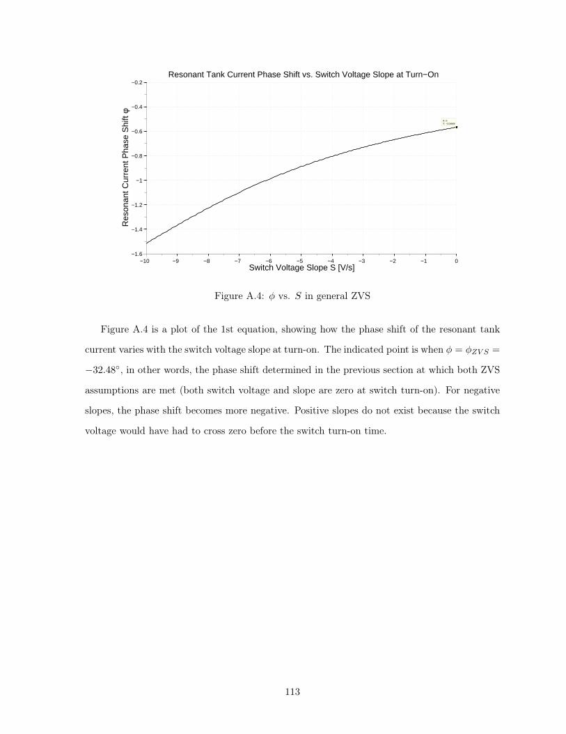
−10 −9 −8 −7 −6 −5 −4 −3 −2 −1 0−1.6
−1.4
−1.2
−1
−0.8
−0.6
−0.4
−0.2
X: 0Y: −0.5669
Switch Voltage Slope S [V/s]
Resonant Tank Current Phase Shift vs. Switch Voltage Slope at Turn−On
Res
onan
t Cur
rent
Pha
se S
hift
φ
Figure A.4: φ vs. S in general ZVS
Figure A.4 is a plot of the 1st equation, showing how the phase shift of the resonant tank
current varies with the switch voltage slope at turn-on. The indicated point is when φ = φZV S =
−32.48, in other words, the phase shift determined in the previous section at which both ZVS
assumptions are met (both switch voltage and slope are zero at switch turn-on). For negative
slopes, the phase shift becomes more negative. Positive slopes do not exist because the switch
voltage would have had to cross zero before the switch turn-on time.
113
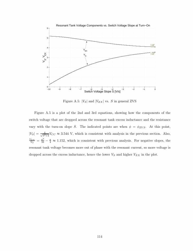
−10 −9 −8 −7 −6 −5 −4 −3 −2 −1 00
1
2
3
4
5
6
X: −0.009Y: 4.085
Switch Voltage Slope S [V/s]
VS, V
EX
Resonant Tank Voltage Components vs. Switch Voltage Slope at Turn−On
X: −0.009Y: 3.544
VEX
VS
Figure A.5: |VS | and |VEX | vs. S in general ZVS
Figure A.5 is a plot of the 2nd and 3rd equations, showing how the components of the
switch voltage that are dropped across the resonant tank excess inductance and the resistance
vary with the turn-on slope S. The indicated points are when φ = φZV S. At this point,
|VS | = 4√π2+4
VCC ≈ 3.544 V, which is consistent with analysis in the previous section. Also,
VEX
VS= π3
16 − π4 ≈ 1.152, which is consistent with previous analysis. For negative slopes, the
resonant tank voltage becomes more out of phase with the resonant current, so more voltage is
dropped across the excess inductance, hence the lower VS and higher VEX in the plot.
114
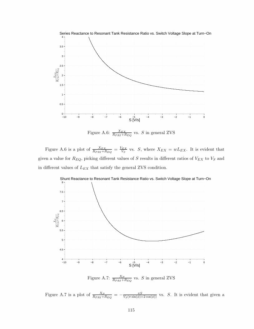
−10 −9 −8 −7 −6 −5 −4 −3 −2 −1 00
0.5
1
1.5
2
2.5
3
3.5
4
S [V/s]
XEX
RPRI+
REQ
Series Reactance to Resonant Tank Resistance Ratio vs. Switch Voltage Slope at Turn−On
Figure A.6: XEX
RPRI+REQvs. S in general ZVS
Figure A.6 is a plot of XEX
RPRI+REQ= VEX
VSvs. S, where XEX = wLEX . It is evident that
given a value for REQ, picking different values of S results in different ratios of VEX to VS and
in different values of LEX that satisfy the general ZVS condition.
−10 −9 −8 −7 −6 −5 −4 −3 −2 −1 04
4.5
5
5.5
6
6.5
7
7.5
8
S [V/s]
XP
RPRI+
REQ
Shunt Reactance to Resonant Tank Resistance Ratio vs. Switch Voltage Slope at Turn−On
Figure A.7: XP
RPRI+REQvs. S in general ZVS
Figure A.7 is a plot of XP
RPRI+REQ= − πS
VS(π sin(φ)+2 cos(φ)) vs. S. It is evident that given a
115
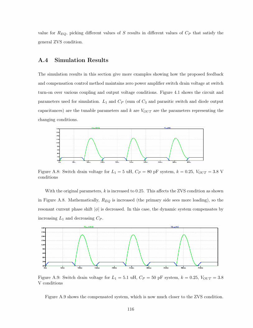
value for REQ, picking different values of S results in different values of CP that satisfy the
general ZVS condition.
A.4 Simulation Results
The simulation results in this section give more examples showing how the proposed feedback
and compensation control method maintains zero power amplifier switch drain voltage at switch
turn-on over various coupling and output voltage conditions. Figure 4.1 shows the circuit and
parameters used for simulation. L1 and CP (sum of C3 and parasitic switch and diode output
capacitances) are the tunable parameters and k are VOUT are the parameters representing the
changing conditions.
Figure A.8: Switch drain voltage for L1 = 5 uH, CP = 80 pF system, k = 0.25, VOUT = 3.8 Vconditions
With the original parameters, k is increased to 0.25. This affects the ZVS condition as shown
in Figure A.8. Mathematically, REQ is increased (the primary side sees more loading), so the
resonant current phase shift |φ| is decreased. In this case, the dynamic system compensates by
increasing L1 and decreasing CP .
Figure A.9: Switch drain voltage for L1 = 5.1 uH, CP = 50 pF system, k = 0.25, VOUT = 3.8V conditions
Figure A.9 shows the compensated system, which is now much closer to the ZVS condition.
116
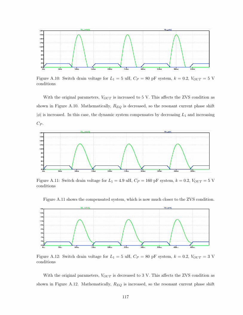
Figure A.10: Switch drain voltage for L1 = 5 uH, CP = 80 pF system, k = 0.2, VOUT = 5 Vconditions
With the original parameters, VOUT is increased to 5 V. This affects the ZVS condition as
shown in Figure A.10. Mathematically, REQ is decreased, so the resonant current phase shift
|φ| is increased. In this case, the dynamic system compensates by decreasing L1 and increasing
CP .
Figure A.11: Switch drain voltage for L1 = 4.9 uH, CP = 160 pF system, k = 0.2, VOUT = 5 Vconditions
Figure A.11 shows the compensated system, which is now much closer to the ZVS condition.
Figure A.12: Switch drain voltage for L1 = 5 uH, CP = 80 pF system, k = 0.2, VOUT = 3 Vconditions
With the original parameters, VOUT is decreased to 3 V. This affects the ZVS condition as
shown in Figure A.12. Mathematically, REQ is increased, so the resonant current phase shift
117
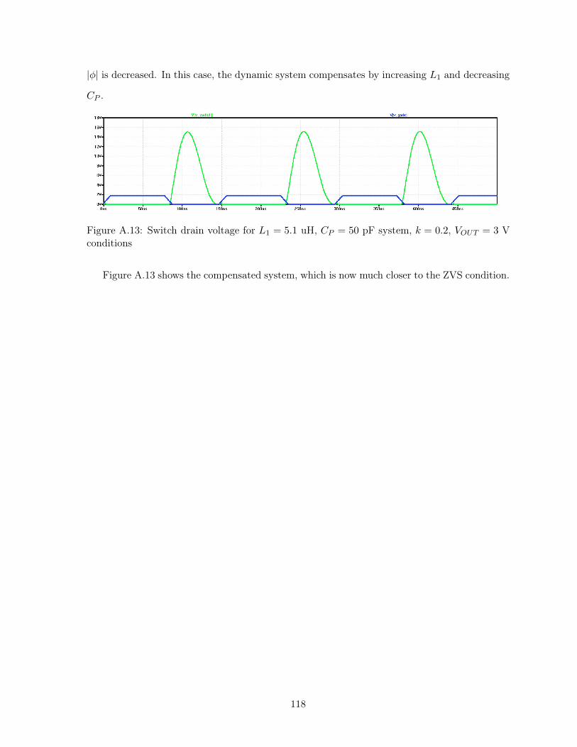
|φ| is decreased. In this case, the dynamic system compensates by increasing L1 and decreasing
CP .
Figure A.13: Switch drain voltage for L1 = 5.1 uH, CP = 50 pF system, k = 0.2, VOUT = 3 Vconditions
Figure A.13 shows the compensated system, which is now much closer to the ZVS condition.
118
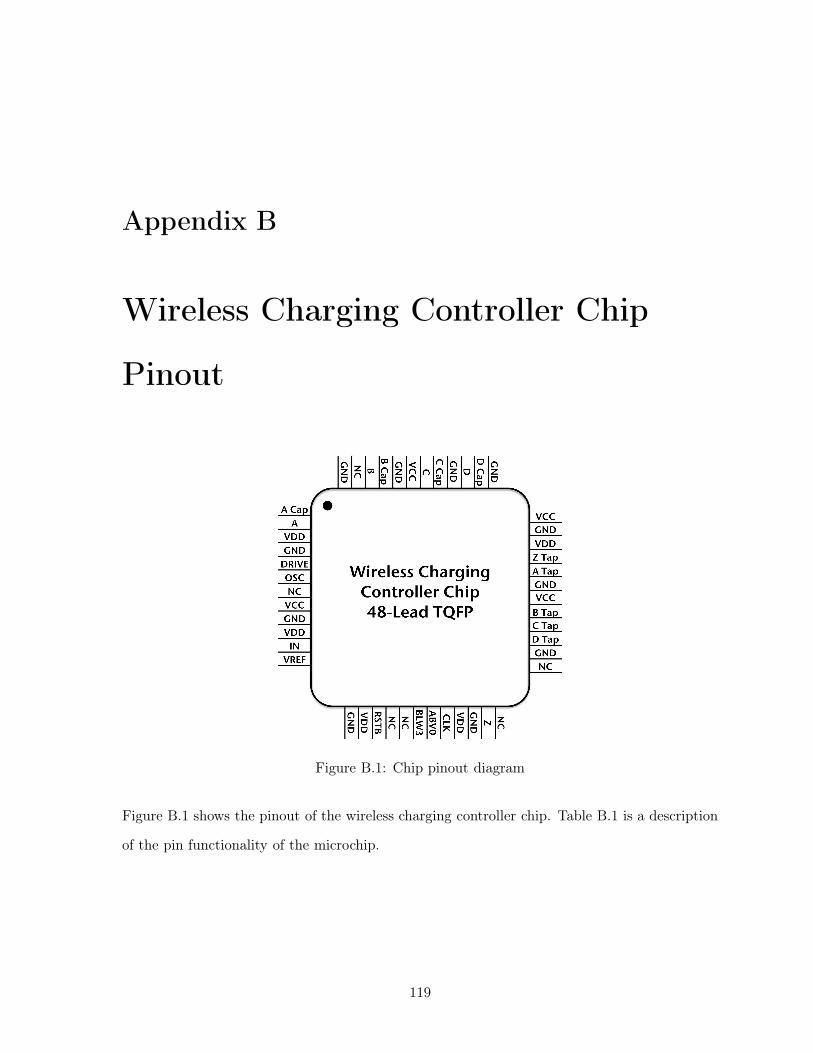
Appendix B
Wireless Charging Controller Chip
Pinout
Figure B.1: Chip pinout diagram
Figure B.1 shows the pinout of the wireless charging controller chip. Table B.1 is a description
of the pin functionality of the microchip.
119
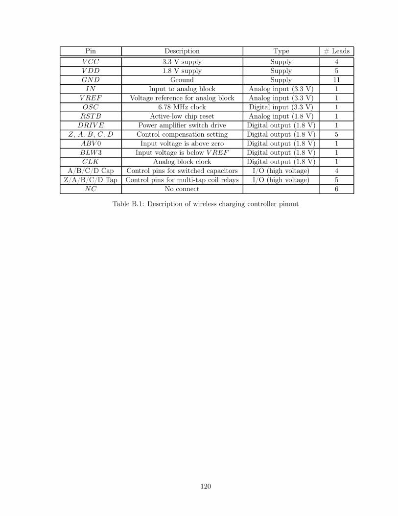
Pin Description Type # Leads
V CC 3.3 V supply Supply 4
V DD 1.8 V supply Supply 5
GND Ground Supply 11
IN Input to analog block Analog input (3.3 V) 1
V REF Voltage reference for analog block Analog input (3.3 V) 1
OSC 6.78 MHz clock Digital input (3.3 V) 1
RSTB Active-low chip reset Analog input (1.8 V) 1
DRIV E Power amplifier switch drive Digital output (1.8 V) 1
Z, A, B, C, D Control compensation setting Digital output (1.8 V) 5
ABV 0 Input voltage is above zero Digital output (1.8 V) 1
BLW3 Input voltage is below V REF Digital output (1.8 V) 1
CLK Analog block clock Digital output (1.8 V) 1
A/B/C/D Cap Control pins for switched capacitors I/O (high voltage) 4
Z/A/B/C/D Tap Control pins for multi-tap coil relays I/O (high voltage) 5
NC No connect 6
Table B.1: Description of wireless charging controller pinout
120

Bibliography
[1] Y. Lo, K. Chen, P. Gad, and W. Liu. A fully-integrated high-compliance voltage SoC forepi-retinal and neural prostheses. IEEE Transactions on Biomedical Circuits and Systems,7(16):761–772, December 2013.
[2] G.A. Kendir, W. Liu, G. Wang, M. Sivaprakasam, R. Bashirullah, M.S. Humayun, and J.D.Weiland. An optimal design methodology for inductive power link with Class-E amplifier.IEEE Transactions on Circuits and Systems I, 52(5):857–866, May 2005.
[3] M.W. Baker and R. Sarpeshkar. Feedback analysis and design of RF power links for low-power bionic systems. IEEE Transactions on Biomedical Circuits and Systems, 1(1):28–38,March 2007.
[4] G. Wang, W. Liu, M. Sivaprakasam, and G.A. Kendir. Design and analysis of an adaptivetranscutaneous power telemetry for biomedical implants. IEEE Transactions on Circuitsand Systems I, 52(10):2109–2117, October 2005.
[5] Cochlear Bone Anchored Solutions AB. 100,000 people aroundthe world can hear again thanks to a Cochlear Baha system.http://cochlear.com/wps/wcm/connect/intl/about/media-centre/100000-people-around-the-world-can-hear-again-thanks-to-a-cochlear-baha-system, August 2013.
[6] Duracell. Duracell PowerMat. http://www.duracellpowermat.com.
[7] Fulton innovation raising the bar for wireless power with new applications for a trulywireless world at 2011 CES, January 2011.
[8] P. Li and R. Bashirullah. A wireless power interface for rechargeable battery operatedmedical implants. IEEE Transactions on Circuits and Systems II, 54(10):912–916, October2007.
[9] D. Kürschner and C. Rathge. Contactless energy transmission systems with improved coilpositioning flexibility for high power applications. Power Electronics Specialists Conference,pages 4326–4332, June 2008.
[10] National Institutes of Health. Cochlear implants, November 2013.
[11] Witricity. Highly resonant wireless power transfer: Safe, efficient, and over distance.
[12] Power Matters Alliance.
[13] Wireless Power Consortium.
121
[14] Frost and Sullivan. San Francisco supervisor takes aim at toxic battery waste. Environ-mental News Network, 2001.
[15] The New York Times. Push for standard cellphone charger gains ground. The New YorkTimes, 2009.
[16] The Freedonia Group. Batteries: Study 2449, January 2009.
[17] M. Kline, I. Izyumin, B. Boser, and S. Sanders. Capacitive power transfer for contactlesscharging. IEEE Applied Power Electronics Conference and Exposition (APEC), pages1398–1404, 2011.
[18] K. Onizuka, H. Kawaguichi, M. Takamiya, T. Kuroda, and T. Sakurai. Chip-to-chipinductive wireless power transmission system for SiP applications. IEEE Custom IntegratedCircuits Conference, pages 575–578, 2006.
[19] P. Mercier and A.P. Chandrakasan. Rapid wireless capacitor charging using a multi-tapped inductively-coupled secondary coil. IEEE Transactions on Circuits and SystemsI, 60(9):2263–2272, 2013.
[20] A. Burke. Ultracapacitors: why, how, and where is the technology. Journal of PowerSources, 91(1):37–50, 2000.
[21] Federal Communications Commission. Title 47, Part 18 - industrial, scientific and medicalequipment.
[22] A. S. Y. Poon, S. O’Driscoll, and T. H. Meng. Optimal frequency for wireless powertransmission into dispersive tissue. IEEE Transactions on Antennas and Propagation,58(5):1739–1750, May 2010.
[23] MED-EL. Maestro 2010.
[24] M. Kiani, U. Jow, and M. Ghovanloo. Design and optimization of a 3-coil inductive linkfor efficient wireless power transmission. IEEE Transactions on Biomedical Circuits andSystems, 5(6):579–591, December 2011.
[25] R. Shaffer. Fundamentals of power electronics with MATLAB. Charles River Media, 2007.
[26] S. Guo and H. Lee. An efficiency-enhanced CMOS rectifier with unbalanced-biased com-parators for transcutaneous-powered high-current implants. IEEE Journal of Solid-StateCircuits, 44(6):1796–1804, June 2009.
[27] Y. Lam, W. Ki, and C. Tsui. Integrated low-loss CMOS active rectifier for wirelessly pow-ered devices. IEEE Transactions on Circuits and Systems II, 53(12):1378–1382, December2006.
[28] S. Hashemi, M. Sawan, and Y. Savaria. Fully-integrated low-voltage high-efficiency CMOSrectifier for wirelessly powered devices. Joint IEEE North-East Workshop on Circuits andSystems and TAISA Conference, pages 1–4, July 2009.
[29] G. Gosset and D. Flandre. A very high efficiency ultra-low-power 13.56MHz voltage rectifierin 150nm SOI CMOS. IEEE International Symposium on Radio-Frequency IntegrationTechnology, pages 347–350, 2009.
122
[30] C. Peters, J. Handwerker, D. Maurath, and Y. Manoli. A sub-500 mV highly efficient activerectifier for energy harvesting applications. IEEE Transactions on Circuits and Systems I,58(7):1542–1550, July 2011.
[31] F. H. Raab. Effects of circuit variations on the Class E tuned power amplifier. IEEEJournal of Solid-State Circuits, 13(2):239–247, April 1978.
[32] P. Keshri and B. Deka. CMOS thyristor based low frequency ring oscillator. Technicalreport, Indian Institute of Technology, Kanpur.
[33] H. Chung, A. Radecki, N. Miura, H. Ishikuro, and T. Kuroda. A 0.025–0.45 W 60%-efficiency inductive-coupling power transceiver with 5-bit dual-frequency feedforward con-trol for non-contact memory cards. IEEE Journal of Solid-State Circuits, 47(10):2496–2504,October 2012.
[34] H. Lee, K. Kwon, W. Li, and M. Ghovanloo. A power-efficient switched-capacitor stimu-lating system for electrical/optical deep-brain stimulation. IEEE International Solid-StateCircuits Conference (ISSCC), pages 414–416, 2014.
[35] M. Ghovanloo and S. Atluri. A wide-band power-efficient inductive wireless link for im-plantable microelectronic devices using multiple carriers. IEEE Transactions on Circuitsand Systems I, 54(10):2211–2221, October 2007.
[36] M. Catrysse, B. Hermans, and R. Puers. An inductive power system with integratedbi-directional data-transmission. Sensors and Actuators A, 115:221–229, 2004.
[37] Alliance For Wireless Power.
[38] iFixit. Fitbit Flex teardown, 2013.
[39] IHS Electronics and Media. Teardown: Fitbit Flex, October 2013.
[40] M. Yip, R. Jin, H.H. Nakajima, K.M. Stankovic, and A.P. Chandrakasan. A fully-implantable cochlear implant SoC with piezoelectric middle ear sensor and energy-efficientstimulation in 0.18 um HVCMOS. IEEE International Solid-State Circuits Conference(ISSCC), pages 312–313, 2014.
[41] L.S.Y. Wong, S. Hossain, A. Ta, J. Edvinsson, D.H. Rivas, and H. Nääs. A very low-power CMOS mixed-signal IC for implantable pacemaker applications. IEEE Journal ofSolid-State Circuits, 39(12):2446–2456, December 2004.
[42] T.J. Sullivan, S.R. Deiss, and G. Cauwenberghs. A low-noise, non-contact EEG/ECGsensor. Biomedical Circuits and Systems Conference (BIOCAS), pages 154–157, 2007.
[43] M. Guanying, Y. Guozheng, and H. Xiu. Power transmission for gastrointestinal microsys-tems using inductive coupling. Physiological Measurement, 28:9–18, 2007.
[44] iFixit. iPod Shuffle 4th generation teardown, 2010.
[45] Instructables. Ti-84 basic disassembly, 2008.
[46] M. Chen, S. Gonzalez, A. Vasilakos, H. Cao, and V.C.M. Leung. Body area networks: Asurvey. Mobile Networks and Applications, 16(2):171–193, April 2011.
123

[47] B. Latré, B. Braem, I. Moerman, C. Blondia, and P. Demeester. A survey on wireless bodyarea networks. Wireless Networks, 17(1):1–18, January 2011.
[48] M. Klemm and G. Troester. Textile UWB antennas for wireless body area networks. IEEETransactions on Antennas and Propagation, 54(11):3192–3197, November 2006.
[49] J. Ryckaert, C. Desset, A. Fort, M. Badaroglu, V. De Heyn, P. Wambacq, G. Van der Plas,S. Donnay, B. Van Poucke, and B. Gyselinckx. Ultra-wide-band transmitter for low-powerwireless body area networks: Design and evaluation. IEEE Transactions on Circuits andSystems I, 52(12):2515–2525, December 2005.
[50] M. Li, W. Lou, and K. Ren. Data security and privacy in wireless body area networks.Wireless Communications, IEEE, 17(1):51–58, February 2010.
[51] B. Gyselinckx, C. Van Hoof, J. Ryckaert, R.F. Yazicioglu, P. Fiorini, and V. Leonov. Hu-man++: Autonomous wireless sensors for body area networks. Custom Integrated CircuitsConference, pages 13–19, 2005.
[52] S. De and R. Singhal. Toward uninterrupted operation of wireless sensor networks. Com-puter, 45(9):24–30, September 2012.
[53] N. Desai. A low-power, reconfigurable fabric body area network for healthcare applications.Master’s thesis, Massachusetts Institute of Technology, 2012.
[54] J. Cheng, L. Xia, C. Ma, Y. Lian, X. Xu, C.P. Yue, Z. Hong, and P.Y. Chiang. A near-threshold, multi-node, wireless body area sensor network powered by RF energy harvesting.Custom Integrated Circuits Conference (CICC), 2012.
[55] R. Zhang and C.K. Ho. MIMO broadcasting for simultaneous wireless information andpower transfer. IEEE Transactions on Wireless Communications, 12(5):1989–2001, May2013.
[56] A. Kurs, A. Karalis, R. Moffatt, J.D. Joannopoulos, P. Fisher, and M. Soljacic. Wirelesspower transfer via strongly coupled magnetic resonances. Science, 317(83):83–86, July2007.
[57] A. Karalis, J.D. Joannopoulos, and Marin Soljacic. Efficient wireless non-radiative mid-range energy transfer. Annals of Physics, 323:34–48, 2008.
[58] C. Zhu, K. Liu, C. Yu, R. Ma, and H. Cheng. Simulation and experimental analysis onwireless energy transfer based on magnetic resonances. IEEE Vehicle Power and PropulsionConference (VPPC), September 2008.
[59] K. Fotopoulou and B.W. Flynn. Wireless power transfer in loosely coupled links: Coilmisalignment model. IEEE Transactions on Magnetics, 47(2):416–430, February 2011.
[60] K.Y. Kim, Y. Ryu, E. Park, K. Song, and C. Ahn. Analysis of misalignments in efficiencyof mid-range magnetic resonance wireless power link. IEEE Antennas and PropagationSociety International Symposium (APSURSI), pages 1–2, 2012.
[61] A.P. Sample, D.A. Meyer, and J.R. Smith. Analysis, experimental results, and range adap-tation of magnetically coupled resonators for wireless power transfer. IEEE Transactionson Industrial Electronics, 58(2):544–554, February 2011.
124

[62] B.L. Cannon, J.F. Hoburg, D.D. Stancil, and S.C. Goldstein. Magnetic resonant coupling asa potential means for wireless power transfer to multiple small receivers. IEEE Transactionson Power Electronics, 24(7):1819–1825, July 2009.
[63] J.J. Casanova, Z.N. Low, and J. Lin. A loosely coupled planar wireless power system formultiple receivers. IEEE Transactions on Industrial Electronics, 56(8):3060–3068, August2009.
[64] H. Deng, W. Li, and D.P. Agrawal. Routing security in wireless ad hoc networks. IEEECommunications Magazine, 40(10):70–75, December 2002.
[65] A. Perrig, J. Stankovic, and D. Wagner. Security in wireless sensor networks. Communi-cations of the ACM, 47:53–57, June 2004.
[66] A.P. Chandrakasan, D.C. Daly, J. Kwong, and Y.K. Ramadass. Next generation micro-power systems. Symposium on VLSI Circuits, pages 2–5, 2008.
[67] I.F. Zambari, C.Y. Hui, and R. Mohamed. Development of wireless energy transfer modulefor solar energy harvesting. Procedia Technology, 11:882–894, 2013.
125