Embed Size (px)
Citation preview

Chris A. Mack, Fundamental Principles of Optical Lithography, (c) 2007
1
Resist
Substrate
Air n1
D z = 0
Resist
Substrate
Air EI
n2
n3
Figure 4.1 Film stack showing (a) the geometry for the standing wave derivation, and (b) a normally incident electric field EI.
(a) (b)

Chris A. Mack, Fundamental Principles of Optical Lithography, (c) 2007
2
0.0
0.2
0.4
0.6
0.8
1.0
1.2
1.4
1.6
1.8
0 200 400 600 800 1000
Depth into Resist (nm)
Rel
ativ
e In
tens
ity
Figure 4.2 Standing wave intensity in one micron of photoresist on a silicon substrate for an i-line exposure.

Chris A. Mack, Fundamental Principles of Optical Lithography, (c) 2007
3
0.0
0.2
0.4
0.6
0.8
1.0
1.2
1.4
1.6
0 200 400 600 800 1000
Depth into Resist (nm)
Rel
ativ
e In
ten
sity
Figure 4.3 Standing wave intensity within a photoresist film at the start of exposure (850nm of resist on 100nm SiO2 on silicon, = 436nm). Note the impact of the oxide film on the phase of the effective substrate reflectivity, which affects the intensity at the bottom of the resist.

Chris A. Mack, Fundamental Principles of Optical Lithography, (c) 2007
4
z
x
(x,z)
Substrate
x
z = 0
Plane wave
k
r
Figure 4.4 Geometry used for describing plane waves and standing waves for oblique incidence.

Chris A. Mack, Fundamental Principles of Optical Lithography, (c) 2007
5
0.00
0.05
0.10
0.15
0.20
0.25
0.30
0.35
0.40
0.45
0.50
0 10 20 30 40 50 60 70 80 90
Incident Angle (degrees)
Inte
nsi
ty R
efle
ctiv
ity (
|12
|2 )
p-polarization
s-polarization
air
resist
p-polarization
s-pol.
Figure 4.5 Reflectivity (square of the reflection coefficient) as a function of the angle of incidence showing the difference between s- and p-polarization (n1 = 1.0, n2 = 1.7). Both air and resist layers are assumed to be infinitely thick.

Chris A. Mack, Fundamental Principles of Optical Lithography, (c) 2007
6
0.0
0.5
1.0
1.5
2.0
2.5
0 100 200 300 400 500
Depth into Resist (nm)
Rel
ativ
e In
tens
ity
angle = 0 angle = 30
Figure 4.6 Standing wave intensity within a photoresist film (500 nm of resist on silicon, = 248 nm) as a function of incident angle (s-polarization assumed).

Chris A. Mack, Fundamental Principles of Optical Lithography, (c) 2007
7
0.0
0.2
0.4
0.6
0.8
1.0
200 250 300 350 400 450 500 550 600
Wavelength (nm)
Re
lativ
e In
ten
sity
I-Line
H-Line G-Line
E-Line
Figure 4.7 Spectral output of a typical high-pressure mercury arc lamp. The illumination spectrum of an i-line or g-line lithographic exposure tool is usually a filtered portion of this lamp spectrum.
Chris A. Mack, Fundamental Principles of Optical Lithography, (c) 2007
8
0.0
0.5
1.0
1.5
2.0
2.5
3.0
0 200 400 600 800 1000
Depth into Resist (nm)
Rel
ativ
e In
tens
ity
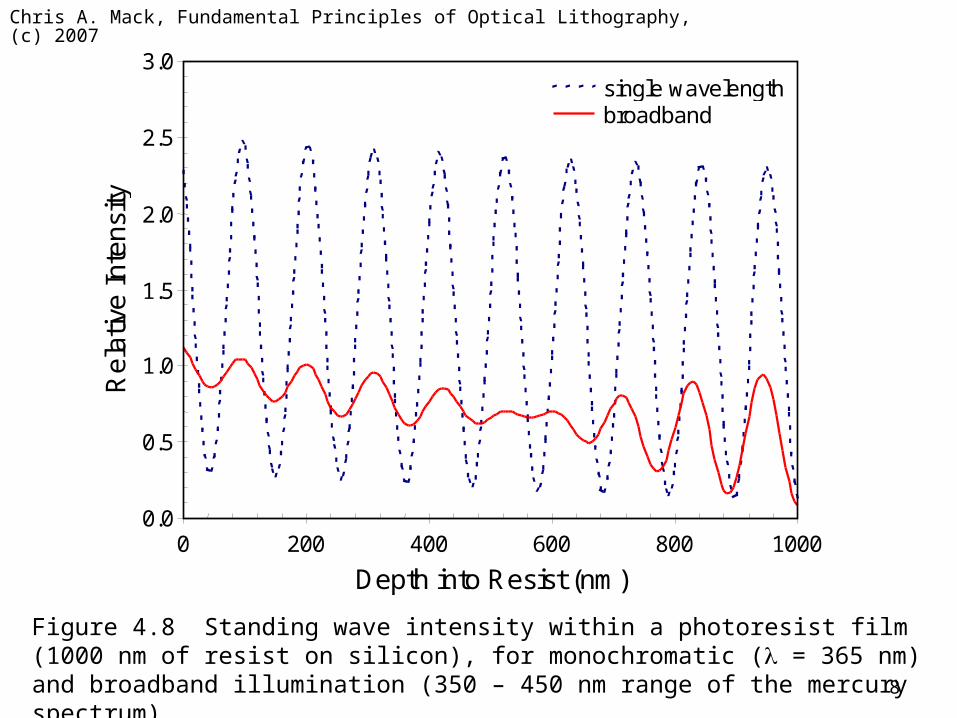
single wavelength broadband
Figure 4.8 Standing wave intensity within a photoresist film (1000 nm of resist on silicon), for monochromatic ( = 365 nm) and broadband illumination (350 – 450 nm range of the mercury spectrum).
Chris A. Mack, Fundamental Principles of Optical Lithography, (c) 2007
9
0.40
0.45
0.50
0.55
0.60
0.65
0.90 0.95 1.00 1.05 1.10 1.15 1.20
Resist Thickness (m)
Re
sist
Lin
ew
idth
(m
)
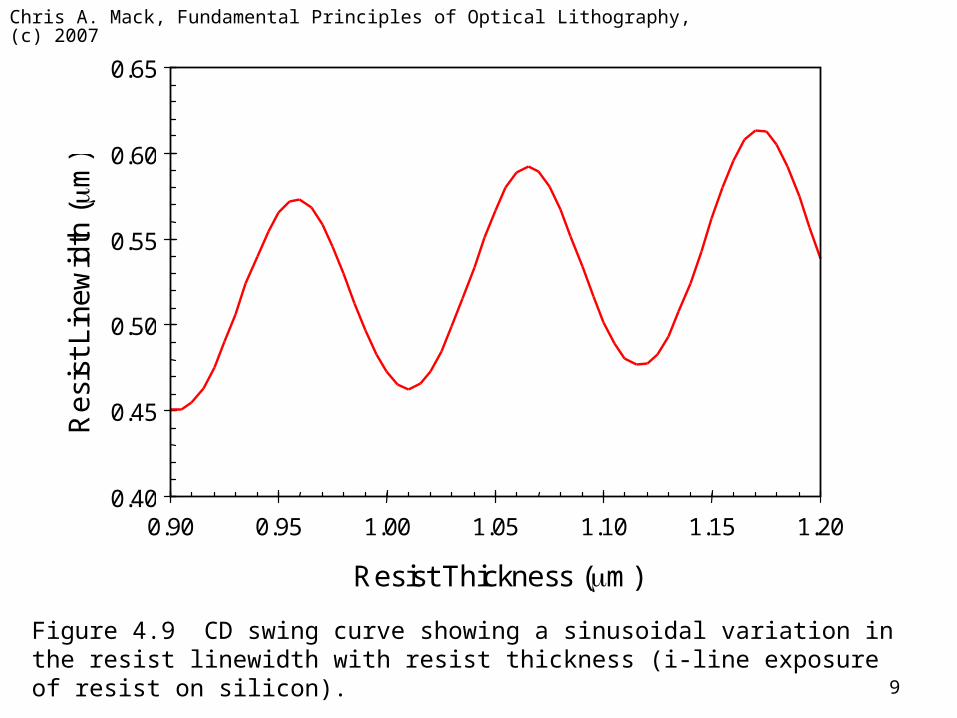
Figure 4.9 CD swing curve showing a sinusoidal variation in the resist linewidth with resist thickness (i-line exposure of resist on silicon).

Chris A. Mack, Fundamental Principles of Optical Lithography, (c) 2007
10
40
50
60
70
80
90
100
0.90 0.95 1.00 1.05 1.10 1.15 1.20
Resist Thickness (m)
Do
se t
o C
lea
r (m
J/cm
2 )
Figure 4.10 Eo swing curve showing a sinusoidal variation in the resist dose-to-clear with resist thickness (i-line exposure of resist on silicon).

Chris A. Mack, Fundamental Principles of Optical Lithography, (c) 2007
11
0.00
0.05
0.10
0.15
0.20
0.25
0.30
0.90 0.95 1.00 1.05 1.10 1.15 1.20
Resist Thickness (m)
Re
flect
ivity
Figure 4.11 Reflectivity swing curve showing a sinusoidal variation in the resist coated wafer reflectivity with resist thickness (i-line exposure of resist on silicon).
Chris A. Mack, Fundamental Principles of Optical Lithography, (c) 2007
12
Resist
Substrate
Air n1
D z = 0
EI Er0
n2
n3
Resist
Substrate
Air Er1
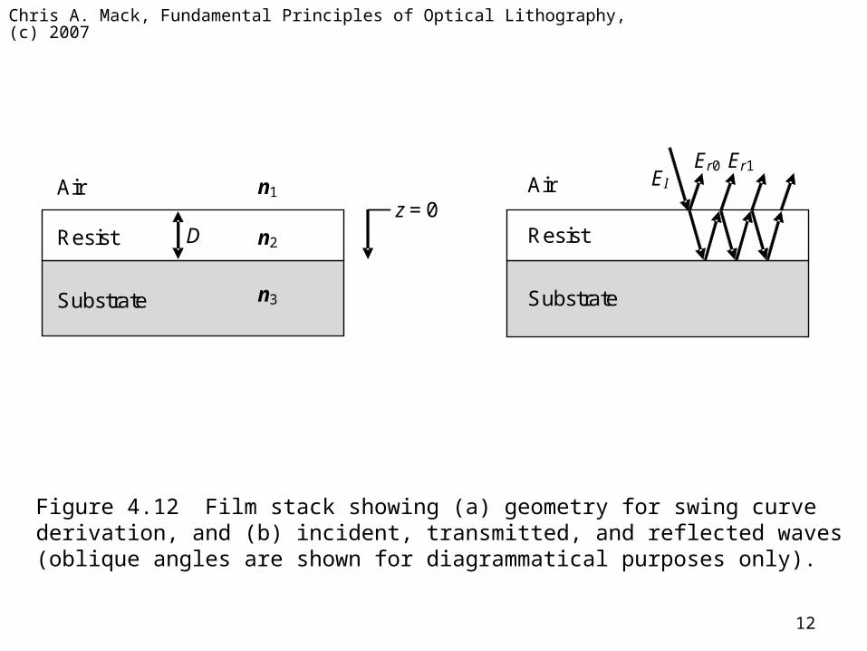
Figure 4.12 Film stack showing (a) geometry for swing curve derivation, and (b) incident, transmitted, and reflected waves (oblique angles are shown for diagrammatical purposes only).

Chris A. Mack, Fundamental Principles of Optical Lithography, (c) 2007
13
1.00 1.05 1.10 1.15 1.20 90
100
110
120
130
140
150
Do
se-t
o-C
lea
r, E
0 (m
J/cm
2 )
Resist Thickness (microns)
NA = 0.2 NA = 0.3 NA = 0.4 NA = 0.5
NA = 0.0
Figure 4.13 The phase and amplitude of a dose-to-clear swing curve are affected by the range of angles striking the resist, which is controlled by the product of the partial coherence and the numerical aperture (NA) for conventional illumination.
Chris A. Mack, Fundamental Principles of Optical Lithography, (c) 2007
14
140
160
180
200
220
240
260
200 220 240 260 280 300 320 340 360 380 400
Re
sist
Fe
atu
re W
idth
, CD
(n
m)
Resist Thickness (nm)
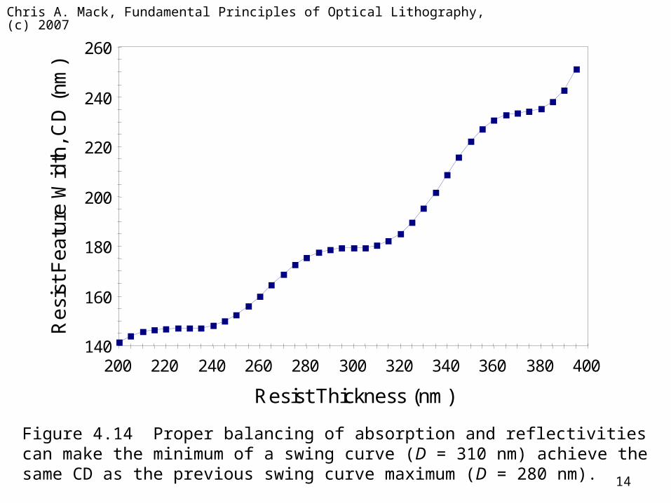
Figure 4.14 Proper balancing of absorption and reflectivities can make the minimum of a swing curve (D = 310 nm) achieve the same CD as the previous swing curve maximum (D = 280 nm).
Chris A. Mack, Fundamental Principles of Optical Lithography, (c) 2007
15
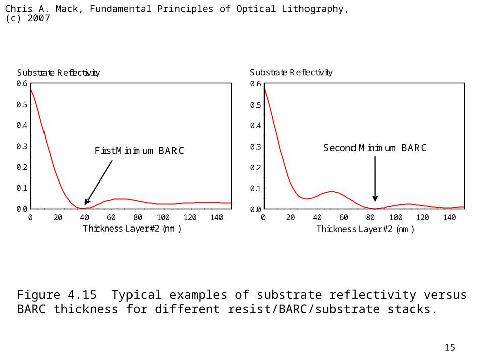
Substrate Reflectivity
Thickness Layer #2 (nm)
Second Minimum BARC First Minimum BARC
0.0
0.1
0.2
0.3
0.4
0.5
0.6 Substrate Reflectivity
Thickness Layer #2 (nm) 0 20 40 60 80 100 120 140 0 20 40 60 80 100 120 140
0.0
0.1
0.2
0.3
0.4
0.5
0.6
Figure 4.15 Typical examples of substrate reflectivity versus BARC thickness for different resist/BARC/substrate stacks.

Chris A. Mack, Fundamental Principles of Optical Lithography, (c) 2007
16
1.0
1.2
1.4
1.6
1.8
2.0
2.2
2.4
2.6
10 20 30 40 50 60
BARC Thickness (nm)
Ref
ract
ive
Inde
x -
real
0.30
0.35
0.40
0.45
0.50
0.55
0.60
0.65
0.70
0.75
0.80
Ref
ract
ive
Inde
x -
imag
inar
y
n
1.2
1.4
1.6
1.8
2.0
2.2
2.4
2.6
2.8
50 70 90 110 130
BARC Thickness (nm)
Ref
ract
ive
Inde
x -
real
0.16
0.21
0.26
0.31
0.36
0.41
Ref
ract
ive
Inde
x -
imag
inar
y
n
(a) (b)
Figure 4.16 Optimum BARC refractive index (real and imaginary parts, n and k) as a function of BARC thickness for normal incidence illumination (resist index = 1.7 + i0.01536 and silicon substrate index = 0.8831 + i2.778) at 193 nm. a) First minimum BARCs, and b) second minimum BARCs.

Chris A. Mack, Fundamental Principles of Optical Lithography, (c) 2007
17
0.000
0.001
0.002
0.003
0.004
0.005
0 20 40 60 80
Optimum BARC Thickness (nm)
R/
2 (1
/nm
2 )
0.0
0.2
0.4
0.6
0.8
1.0
1.2
1.4
0 10 20 30 40 50 60 70
Optimum BARC Thickness (nm)
R/|n
|2 (a) (b)
Figure 4.17 Sensitivity of substrate reflectivity for the optimum first minimum BARCs of Figure 4.16a as a function of a) BARC thickness errors, or b) BARC refractive index errors.

Chris A. Mack, Fundamental Principles of Optical Lithography, (c) 2007
18
0.0000
0.0002
0.0004
0.0006
0.0008
0.0010
0.0012
0.0014
0.0016
50 70 90 110 130
Optimum BARC Thickness (nm)
R/
2 (
1/n
m2)
0.0
0.5
1.0
1.5
2.0
2.5
50 70 90 110 130
Optimum BARC Thickness (nm)
R/|n
|2
(a) (b)
Figure 4.18 Sensitivity of substrate reflectivity for the optimum second minimum BARCs of Figure 4.16b as a function of a) BARC thickness errors, or b) BARC refractive index errors.

Chris A. Mack, Fundamental Principles of Optical Lithography, (c) 2007
19
2.10
2.11
2.12
2.13
2.14
2.15
2.16
2.17
2.18
2.19
2.20
0 10 20 30 40 50 60 70
Angle (in air, degrees)
Re
fra
ctiv
e In
dex
- re
al
0.665
0.670
0.675
0.680
0.685
0.690
0.695
0.700
0.705
0.710
0.715
0.720
Re
fra
ctiv
e In
dex
- im
agin
ary
n
D = 20 nm
1.50
1.52
1.54
1.56
1.58
1.60
1.62
1.64
1.66
1.68
0 10 20 30 40 50 60 70
Angle (in air, degrees)
Re
fra
ctiv
e In
dex
- re
al
0.475
0.480
0.485
0.490
0.495
0.500
0.505
0.510
Re
fra
ctiv
e In
dex
- im
ag
ina
ry
n
D = 40 nm
(a) (b)
Figure 4.19 Optimum BARC parameters to achieve minimum substrate reflectivity as a function of incident angle (angle defined in air, before entering the photoresist) for two different BARC thicknesses (resist index = 1.7 + i0.01536 and silicon substrate index = 0.8831 + i2.778) at 193 nm exposure: a) 20 nm BARC thickness, and b) 40 nm BARC thickness.

Chris A. Mack, Fundamental Principles of Optical Lithography, (c) 2007
20
0.0000
0.0005
0.0010
0.0015
0.0020
0.0025
0.0030
0 10 20 30 40 50 60 70
Angle (in air, degrees)
Min
imu
m In
ten
sity
Re
flect
ivity
D = 20nm
D = 40nm
Figure 4.20 The best case (minimum) reflectivity (using the BARC parameters shown in Figure 4.19) of the substrate as a function of incident angle for 20nm and 40nm thick BARC films. Note that 60º corresponds to the maximum angle in air allowed for NA = 0.866.

Chris A. Mack, Fundamental Principles of Optical Lithography, (c) 2007
21
0.00
0.05
0.10
0.15
0.20
0 10 20 30 40 50 60 70 80
Angle in Air (degrees)
Re
sist
/BA
RC
Ele
ctric
Fie
ld R
efle
ctiv
ity
A: p-polarized
A: s-polarized
B: s-polarized
B: p-polarized
Figure 4.21 An example of the variation of BARC reflectivity as a function of light angle and polarization for two different BARCs. The intensity reflectivity is the square of the electric field reflectivity plotted here, but interference makes the field reflectivity a better measure of the standing wave effects. (Resist index = 1.7 + i0.01536, silicon substrate index = 0.8831 + i2.778, BARC A index = 1.80 + i0.48, BARC A thickness = 30 nm, BARC B index = 1.53 + i0.54, BARC B thickness = 39 nm.)

Chris A. Mack, Fundamental Principles of Optical Lithography, (c) 2007
22
0.0
0.1
0.2
0.3
0.4
0.5
0.6
0.7
0 20 40 60 80 100 120 140
100 105 110 115 120 125 130 135 140 145 150 155 160 165 170 175 180 185 190 195 200
Oxide Thickness S
ubst
rate
Ref
lect
ivity
Thickness Layer #2 (nm)
100 105 110 115 120 125 130 135 140 145 150 155 160 165 170 175 180 185 190 195 200
100 105 110 115 120 125 130 135 140 145 150 155 160 165 170 175 180 185 190 195 200
Figure 4.22 Substrate reflectivity versus BARC thickness over a range of underlying oxide thicknesses (oxide on top of a silicon substrate).

Chris A. Mack, Fundamental Principles of Optical Lithography, (c) 2007
23
80
90
100
110
120
130
Re
sist
Fe
atu
re W
idth
, CD
(n
m)
Resist Thickness (nm)
R = 0.43%
R = 0.07%
150 160 170 180 190 200 210 220 230 240 250
Figure 4.23 CD swing curves (100nm lines with a 280nm pitch are printed with a stepper using annular illumination, with a center sigma given by NA = 0.54) for two different BARCs with different levels of optimization, as given by the resulting substrate reflectivity R.

Chris A. Mack, Fundamental Principles of Optical Lithography, (c) 2007
24
Swing Curve Maximum
Top View
Side View resist
Swing Curve Minimum
Top of Step Bottom of Step
or
Figure 4.24 Example of how resist thickness variations over topography produce linewidth variations due to swing curve effects when a BARC is not used.

Chris A. Mack, Fundamental Principles of Optical Lithography, (c) 2007
25
resist
Figure 4.25 Reflective notching occurs when nearby topography reflects light obliquely into an adjacent photoresist feature.

Chris A. Mack, Fundamental Principles of Optical Lithography, (c) 2007
26
Figure 4.26 Imaging of lines and spaces over reflective topography without BARC (left) showing reflective notching, and with BARC (right) showing the reflective notching effectively suppressed (photos courtesy of AZ Photoresist, used with permission).

Chris A. Mack, Fundamental Principles of Optical Lithography, (c) 2007
27
Image Transmitted Through the CEL
CEL
Incident Aerial Image
Figure 4.27 Contrast Enhancement Layer (CEL) bleaching improves the quality of the aerial image transmitted into the photoresist.

Chris A. Mack, Fundamental Principles of Optical Lithography, (c) 2007
28
25 75 125 175 225 0.65
0.70
0.75
0.80
0.85 M
ag
nitu
de
, |
|
Nitride Thickness (nm)
-200
-100
0
100
200
Ph
ase
(d
eg
ree
s)
Figure 4.28 Variation of the magnitude and phase of the resist/substrate reflection coefficient as a function of silicon nitride thickness for a film stack of resist on nitride on 40 nm of oxide on silicon.

Chris A. Mack, Fundamental Principles of Optical Lithography, (c) 2007
29
0.90 0.95 1.00 1.05 1.10
Do
se t
o C
lea
r (m
J/cm
2 )
Resist Thickness (microns)
93nm Nitride
136nm Nitride
75
100
125
150
175
Figure 4.29 Changes in nitride thickness cause a shift in the phase of the resist swing curve, making nitride thickness control as critical as resist thickness control.

Chris A. Mack, Fundamental Principles of Optical Lithography, (c) 2007
30
25 75 125 175 225 0.0
0.2
0.4
0.6
0.8
1.0
Su
bst
rate
Ref
lect
ivity
Nitride Thickness (nm)
Figure 4.30 Nitride thickness also affects the shape of the resist profile, causing resist footing, undercuts, or vertical profiles. Substrate reflectivity (the square of the magnitude of the reflection coefficient) is shown for comparison.

Chris A. Mack, Fundamental Principles of Optical Lithography, (c) 2007
31
1 E
2 E 1 E
2 E 1 E
2 E
1 E
2 E
TE or s-polarization TM or p-polarization
Figure 4.31 Two plane waves with different polarizations will interfere very differently. For transverse electric (TE) polarization (electric field vectors pointing out of the page), the electric fields of the two vectors overlap completely regardless of the angle between the interfering beams.
Chris A. Mack, Fundamental Principles of Optical Lithography, (c) 2007
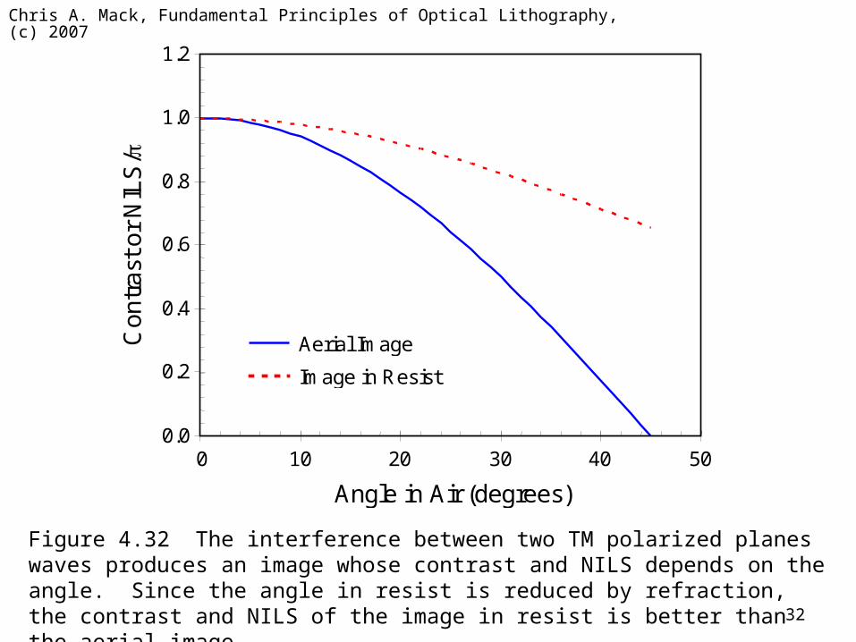
32
0.0
0.2
0.4
0.6
0.8
1.0
1.2
0 10 20 30 40 50
Angle in Air (degrees)
Co
ntr
ast
or
NIL
S/
Aerial Image
Image in Resist
Figure 4.32 The interference between two TM polarized planes waves produces an image whose contrast and NILS depends on the angle. Since the angle in resist is reduced by refraction, the contrast and NILS of the image in resist is better than the aerial image.

Chris A. Mack, Fundamental Principles of Optical Lithography, (c) 2007
33
Figure 4.33 Focusing of plane waves arriving at different angles a) in air, and b) in resist, showing that the resist induces spherical aberration.
(a) (b)

Chris A. Mack, Fundamental Principles of Optical Lithography, (c) 2007
34
0.00
0.05
0.10
0.15
0.20
0.25
0.30
-100 -80 -60 -40 -20 0 20 40 60 80 100
Horizontal Position (nm)
SW
AR
Line Edge
2(0)
Mask
Line Edge
Center of
Space
Figure 4.34 The standing wave amplitude ratio (SWAR) at different positions on the feature for coherent three-beam imaging and s-polarization. For this example of three-beam imaging of 100 nm lines and spaces, ao = 0.5, a1 = 0.3183.

Chris A. Mack, Fundamental Principles of Optical Lithography, (c) 2007
35
0.0 0 20 40 60 80
Incident Angle (degrees)
T o
r I t/
I i
0.2
0.4
0.6
0.8
1.0
It/Ii, s-pol.
It/Ii, p-pol.
T, p-pol. T, s-pol.
Figure 4.35 Intensity transmitted into layer 2 relative to the incident intensity (solid lines) and the transmittance T (dashed lines) as a function of the angle of incidence for both s and p polarization (n1 = 1.0, n2 = 1.5).


![2 LASER INTERFERENCE LITHOGRAPHY - uni-halle.de · 2 LASER INTERFERENCE LITHOGRAPHY (LIL) 9 2 LASER INTERFERENCE LITHOGRAPHY (LIL) Laser interference lithography [3~22] (LIL) is a](https://img.pdfslide.us/doc/110x75/5eae180eecc7e273a41a4e88/2-laser-interference-lithography-uni-hallede-2-laser-interference-lithography.jpg)