Embed Size (px)
Citation preview

p‑Type Transparent Conducting Oxide/n-Type SemiconductorHeterojunctions for Efficient and Stable Solar Water OxidationLe Chen,†,‡ Jinhui Yang,†,‡ Shannon Klaus,†,∥ Lyman J. Lee,†,‡ Rachel Woods-Robinson,‡ Jie Ma,†,‡
Yanwei Lum,†,⊥ Jason K. Cooper,†,⊥ Francesca M. Toma,†,¶ Lin-Wang Wang,†,‡ Ian D. Sharp,†,§
Alexis T. Bell,†,∥ and Joel W. Ager*,†,‡
†Joint Center for Artificial Photosynthesis, ‡Materials Sciences Division, ¶Chemical Sciences Division, and §Physical BiosciencesDivision, Lawrence Berkeley National Laboratory, Berkeley, California 94720, United States∥Department of Chemical and Biomolecular Engineering and ⊥Department of Materials Science and Engineering, University ofCalifornia at Berkeley, Berkeley, California 94720, United States
*S Supporting Information
ABSTRACT: Achieving stable operation of photoanodes used ascomponents of solar water splitting devices is critical to realizing thepromise of this renewable energy technology. It is shown that p-typetransparent conducting oxides (p-TCOs) can function both as a selectivehole contact and corrosion protection layer for photoanodes used in light-driven water oxidation. Using NiCo2O4 as the p-TCO and n-type Si as aprototypical light absorber, a rectifying heterojunction capable of light drivenwater oxidation was created. By placing the charge separating junction in theSi using a np+ structure and by incorporating a highly active heterogeneousNi−Fe oxygen evolution catalyst, efficient light-driven water oxidation can beachieved. In this structure, oxygen evolution under AM1.5G illuminationoccurs at 0.95 V vs RHE, and the current density at the reversible potentialfor water oxidation (1.23 V vs RHE) is >25 mA cm−2. Stable operation wasconfirmed by observing a constant current density over 72 h and by sensitivemeasurements of corrosion products in the electrolyte. In situ Raman spectroscopy was employed to investigate structuraltransformation of NiCo2O4 during electrochemical oxidation. The interface between the light absorber and p-TCO is crucial toproduce selective hole conduction to the surface under illumination. For example, annealing to produce more crystallineNiCo2O4 produces only small changes in its hole conductivity, while a thicker SiOx layer is formed at the n-Si/p-NiCo2O4interface, greatly reducing the PEC performance. The generality of the p-TCO protection approach is demonstrated bymultihour, stable, water oxidation with n-InP/p-NiCo2O4 heterojunction photoanodes.
1. INTRODUCTION
The prospect of using sunlight directly to produce chemicalfuels is attractive for providing alternatives to fossil fuels orenabling grid-scale energy storage, both of which are requiredfor a more sustainable energy future.1,2 Both hydrogen3 andhydrocarbons4 have been envisioned as sustainably producedsolar fuels. One scheme to realize this type of direct solar to fuelconversion is to couple a tandem junction solar cell assembly,together with catalysts in a monolithically integrated device.5−8
A typical design uses a p-type semiconductor as thephotocathode, on which the target fuel is produced viareduction of protons to hydrogen or reduction of CO2 toCO or hydrocarbon fuels. The sustained generation of thesesolar fuels requires a source of protons and electrons, which isprovided by oxidation of water on a series-connected n-typesemiconductor photoanode.Fundamentally, several factors make this reaction difficult
and demanding for materials selection of both the photoanodeand photocathode. From a kinetic point of view, the water
oxidation reaction is a challenging four-proton/four-electronprocess.9 Additionally, stability is of primary concern formaterials under water oxidation conditions, particularly at theextreme pH conditions that are used to ensure ion transportwith minimal resistance losses in overall solar water splittingdevices.10 Indeed, in many of the earliest attempts to realizeefficient solar water splitting with a tandem photovoltaicapproach,11 corrosion at the water oxidation photoanodesemerged as a critical issue which remains to this day.12−14
The stability criterion for semiconductor photoelectrodesunder illumination was defined by Gerischer.15 Briefly, amaterial is stable against corrosion in an electrolyte if itsreductive and oxidative decomposition potentials lie in theconduction and valence bands, respectively. Conversely, if thedecomposition potentials reside within the band gap, thematerial is unstable. Using this criterion, a recent ab initio study
Received: April 10, 2015Published: July 10, 2015
Article
pubs.acs.org/JACS
© 2015 American Chemical Society 9595 DOI: 10.1021/jacs.5b03536J. Am. Chem. Soc. 2015, 137, 9595−9603

of a wide range of elemental and compound semiconductorsfound that only a small group of oxides, including TiO2, Fe2O3,and Co3O4, are stable under illuminated water oxidationconditions.16
The prospect of integrating stable materials as protectionlayers on top of otherwise unstable photoanode materials is apotentially attractive approach to overcoming the limitationsassociated with corrosion.14 Indeed, there were efforts in the1970s and 1980s to protect III−V photoanodes with thin filmsof TiO2; the key challenges which emerged from this work werecreating a continuous coating to avoid failure at grainboundaries and tuning the oxide band structure to allow holeconduction to the solid/electrolyte interface.11,17
It is valuable to consider what would form an “ideal”protection layer. A first criterion is that it should form acontinuous layer without pinholes or other flaws that couldallow electrolyte contact to the underlying, unstable, photo-active material. Second, one would desire the transport ofminority holes to the surface to be facile but the transport ofmajority carriers to be blocked. This will reduce the rate ofinterface recombination and thus promote an optimizedphotovoltage. Finally, for geometries in which the photoanodeis illuminated from the front,18 the protection layer should betransparent and possibly have antireflective properties, tomaximize the carrier generation in the active material.19
Regarding the second criterion above, Campet et al.20 havedelineated the general possibilities for interfacial energeticalignment and associated charge transport, which are depictedschematically in Figure 1. In all cases, the n-type photoabsorberis coupled to a stable protective oxide with a higher conductionband edge, so as to create a barrier for electrons and reduceinterface recombination of the photogenerated holes. Threepossibilities are considered for hole transport to the surface. Inthe first case, the valence band of the protection layer is lowerthan that of the absorber, and holes are transported bytunneling, as shown in Figure 1a. This situation has beenrealized recently for water oxidation by Chen et al.21 with thinlayers of TiO2 grown by atomic layer deposition on n-Si.Excellent stability under water oxidation conditions wasachieved at pH 14. However, the thickness of the oxide layerneeds to be carefully controlled, since the tunneling mechanismintroduces a prohibitively large series resistance for films thickerthan a few nm.22,23
The second case uses a protection layer which possesses avalence band below that of the absorber but allows holetransport through a defect band in the surface coating, as shownin Figure 1b. Such a system was demonstrated by Sun andCampet for protecting GaAs (though not for water oxidation)and allows the use of thicker protection layers.24 This schemewas also realized recently for water oxidation by Hu et al.25
using amorphous TiO2 layers applied to a number of absorbers:n-Si, n-GaAs, and n-GaP. The protection layer could be as thickis 140 nm, ruling out a tunneling mechanism, and stabilities ofover 100 h were demonstrated.The third case is band conduction of holes in the protection
layer, as illustrated in Figure 1c. This approach requires that thevalence band of the protection layer be energetically alignedwith or lie higher than that of the light absorber so that valenceband hole transport can proceed without a barrier.26 Thisapproach has some potential advantages. For example, if thehole conduction through the layer is facile and the band gap issufficiently large so as not to absorb visible light, the coatingcould be thicker and perhaps afford better corrosion protection.
These considerations in the third case provide promise forthe use of p-type transparent conducting oxides (p-TCOs) asprotection layers for water oxidation photoanodes. There hasbeen significant recent work in developing p-TCOs foroptoelectronics applications including organic light emittingdiodes26 and transparent electronics.27 In general, the lowercarrier conductivity of p-TCOs, (<100 S/cm),28−30 comparedto n-type TCOs (∼104 S/cm range) such as indium tin oxide(ITO) has limited their commercial application in devicesrequiring lateral conductivity, such as solar cells.31 However, asprotection layers, out of plane charge transport occurs over
Figure 1. Schematic band diagram of hole transport through aprotective oxide layer deposited on an n-type photoanode. Conductionand valence band edges are red and blue lines, respectively, and quasi-Fermi levels are indicated by dotted lines. Three mechanisms for holetransport are depicted: (a) tunneling, (b) defect band conduction, and(c) valence band transport. Adapted from Campet et al.20
Journal of the American Chemical Society Article
DOI: 10.1021/jacs.5b03536J. Am. Chem. Soc. 2015, 137, 9595−9603
9596

scales of 10s of nm, substantially shorter than the μm−mmscale needed for TCOs designed for in-plane transport.Therefore, the conductivity issues that have hindered p-TCOsin the past are less severe, and it is expected that some of thesematerials could be well suited for stabilization of semi-conductors in solar fuel applications.Indeed, there have been a number of recent reports using p-
type oxide materials to protect otherwise unstable photoanodematerials such as n-Si under illuminated water oxidationconditions in basic electrolytes (pH 13−14). For example,Yang et al.32 found that atomic layer deposited thin films ofCoOx stabilized p+-n Si in pH 14 electrolyte. However, therelatively narrow bandgap of CoOx (Eg < 1.6 eV) leads toparasitic light absorption which limits the thickness of thecoating to a few nanometers. There are a number of recentreports employing thin layers of p-type NiO. Sun et al.33 used asemitransparent hole conducting ITO/Au/ITO layer couplingwith an ultrathin NiOx layer to protect n-Si and np+-Siphotoanode. Thicker NiOx layers (50 to hundreds ofnanometers) were used to stabilize np+-Si photoanodes forhundreds to over 1000 h under water oxidation conditions.34,35
However, there is a potential concern with NiOx as the solecomponent of a protection scheme. During electrochemicalcycling, as would occur during diurnal cycles in natural sunlight,NiOx is known to convert to structurally porous Ni(OH)2/NiOOH,36−38 which ultimately could expose the vulnerablephotoanode surface to the corrosive electrolyte.In this study, we demonstrate the concept of a semi-
conductor corrosion protection based on band-edge transport,using NiCo2O4 as the p-type hole conducting material.NiCo2O4 has a smaller bandgap than NiO but higher thanCo3O4 and has a hole conductivity (up to 300 S/cm) at least 2orders of magnitude higher than either NiO or Co3O4.
39 It alsocrystallizes in the spinel structure similar to the less porousCo3O4. It has exceptional chemical stability in basic electrolytesand has been studied as an oxygen evolution (OER) catalystand as an electrode in batteries and supercapacitors.40−42 Manyp-TCOs, including those in the well-studied delafossite family,require a high temperature step, >600 °C, for synthesis.43−45 Incontrast, NiCo2O4 can be synthesized at relatively lowtemperatures (100−400 °C) and thus can be integrated witha wide range of semiconductors, including Si and III-Vs.In this work, we successfully applied NiCo2O4 as the hole
conducting protection layer on Si and InP photoanodes. Theholes generated in the light absorber are able to travel throughthe p-TCO layer and are effectively injected into the OERcatalyst. The integrated water oxidation half-cell systemdemonstrated at least 72 h stability and one of the lowestonset potentials reported for an np+-Si based photoanode forOER. We also investigate the role of the solid/solid interfacebetween the light absorber and the p-TCO layer in achievingefficient carrier collection.
2. EXPERIMENTAL SECTIONA full description of the synthesis and characterization procedures isprovided in the Supporting Information (SI); an overview will be givenhere. Commercially purchased single crystal Si and InP wafers wereused for the light absorber components of the photoanodes; thesurfaces of both are unstable under the illuminated water oxidationconditions employed. The np+-Si structure was fabricated by ionimplantation and rapid thermal annealing. The p-TCO, NiCo2O4, wasdeposited by reactive sputtering. A 40 nm layer of NiCo2O4 was foundto provide both acceptable corrosion protection and optical trans-parency. The substrate was heated during deposition to ca. 70 °C.
Other substrate temperatures were explored (see SI), but 70 °C wasfound to be optimal in terms of the PEC performance. Ni−Fe wasused as an oxygen evolution catalyst; 2 nm films of this material weredeposited by reactive cosputtering at room temperature. Up to 2 h ofelectrochemical cycling (0 to 0.7 V vs Hg/HgO, 10 mV/s) wasperformed on Ni−Fe coated samples to convert the metal Ni−Fe tothe more OER-active Ni−Fe (oxy)hydroxide catalyst prior to testing.We note that the standard etch procedures to remove the native oxideon Si were not employed prior to p-TCO deposition; since thedeposition is performed in an oxygen containing atmosphere in thepresence of energetic ions, we found that some degree of SiOxformation at the Si/p-TCO interface was unavoidable. The bulk ofthe photoelectrochemical (PEC) evaluations were performed with as-grown NiCo2O4 films. We also examined the critical role of theinterface between the semiconductor light absorber and the p-TCO byannealing some samples at 400 °C in an inert atmosphere. Unlessotherwise stated, PEC evaluations were performed with simulatedAM1.5G illumination in aqueous solution at pH 14 in a standard threeelectrode cell.
In addition to standard thin film structural characterizationtechniques, including X-ray diffraction, electron microscopy, andscanning probe microscopy, we also employed methods which couldyield information regarding the interfacial structure and energetics.These included depth-profiling X-ray photoelectron spectroscopy(XPS), measurement of the valence band edge by XPS, and evaluationof the work function of the NiCo2O4, by both XPS and ab initiocalculations, and in situ analysis of the NiCo2O4 layer by Ramanspectroscopy. We also used sensitive detection of corrosion productsin the electrolyte using inductively coupled mass spectroscopy (ICP-MS) to evaluate the stability of the photoanode structures.
3. RESULTS AND DISCUSSION3.1. Structural, Electronic and Optical Properties of
Sputtered NiCo2O4 Thin Films. Transparency of an as-deposited 40 nm NiCo2O4 film on quartz was evaluated bylooking at the transmission spectrum (Figure 2). At wave-
lengths >480 nm, the light transmission is >70%. Thetransmission increases to nearly 80% in the near-infrared,which corresponds to the locations of the bandgaps of Si (1.1μm) and InP (950 nm). The p-type nature of the films wasconfirmed by the observation of positive Seebeck coefficients(Figure S5). A hole concentration in the low 1020 cm−3 rangewas measured by Hall effect. The valence band edge measuredby XPS (Figure S23) is located very close to the surface Fermi
Figure 2. Transmittance spectrum of a 40 nm thick NiCo2O4 filmsputter deposited onto an optically polished quartz wafer.
Journal of the American Chemical Society Article
DOI: 10.1021/jacs.5b03536J. Am. Chem. Soc. 2015, 137, 9595−9603
9597

level, which is also consistent with a high, degenerate, holeconcentration in the NiCo2O4. The hole conduction mecha-nism was found to be polaron hopping (Figure S6), as has beenreported previously for NiCo2O4.
39 Nevertheless, the roomtemperature conductivity was in the range of 50−60 S/cm,which is comparatively high, particularly for a p-TCO depositedat near room temperature conditions.29 If the NiCo2O4 filmwould be the only source of resistance between the lightabsorber and the electrolyte, we estimate a voltage loss of only2 mV at 30 mA/cm2 current density for a 40 nm thick film witha conductivity of 50 S/cm.XPS survey scans of the as-deposited films identified the Ni
to Co ratio as almost 1 to 2 (35:65), shown in Figure S22. Theas-deposited films lacked long-range crystallinity as indicated bythe absence of peaks in the X-ray diffraction (XRD) spectrum(Figure S1). To examine the crystalline structure more closely,NiCo2O4 and its interface with Si was studied by HR-TEM.Figure 3a shows that the as-deposited films are characterized bycrystalline grains in the size regime of 2−4 nm. In comparison,postdeposition thermal annealing of the NiCo2O4 at 400 °C inargon yields larger and more prominent grains, as shown inFigure 3b. This result is consistent with corresponding XRDpatterns, which reveal the emergence of crystalline peaks(Figure S1), and atomic force micrographs, which also exhibit amore granular morphology than the as grown samples (FigureS3).In both as-deposited and annealed heterostructures,
amorphous SiOx layers are observed at the Si/p-TCO interfaceby HRTEM. The SiOx layer at the as-grown NiCo2O4/Siinterface is <2 nm thick, which is typical for a native oxide onSi. In contrast, the SiOx layer at the annealed NiCo2O4/Siinterface increases to a thickness of 3−4 nm. Further evidenceof a thicker oxide layer was provided by depth-profiling XPS, asshown in Figure S25. Additionally, in Figure 3b, dark regionsextend across the NiCo2O4/SiOx interface into the SiOx layerwhich may be due to some amount of oxygen or metal atomdiffusion.3.2. Photoelectrochemical Evaluation of NiCo2O4 As a
Hole Conducting Protection Layer on Si. For p+-Si/p-NiCo2O4 junctions, we expect an ohmic contact due to highcarrier concentration on both sides of the junction. This isdemonstrated by the black curve in Figure 4a, which is a darkcyclic voltammogram (CV) scan of p+ Si coated with 40 nm ofNiCo2O4. The anodic current rises steeply from an onset near+1.6 V vs RHE, showing that the NiCo2O4 makes a lowresistance contact to p+-Si conducts into the electrolyte.In order to provide further insights on the band diagram of
our heterojunction, we used both theoretical calculations basedon spin-polarized density functional theory (see Figure S26)and the measurement of secondary electron cutoff measured byXPS (Figure S24). The calculated work function is 4.42 eV,which is consistent with XPS measurement of 4.4 ± 0.1 eV.This places the Fermi level of the p-TCO within the bandgap ofSi. A calculated band diagram is shown in Figure 5, the detailsof the calculation are provided in the SI. There is a modestamount of predicted upward band bending in the n-Si, implyingthat the junction should be rectifying. Indeed, this is observedin both photovoltaic (Figure S7) and PEC measurements. Theblue curve in Figure 4a is the illuminated CV of a n-Si(100)/p-NiCo2O4 photoanode. There is a cathodic shift of the CV curveof about 150 mV compared to the p+ Si/NiCo2O4 structure,which is consistent with the rectification predicted by the banddiagram in Figure 5a. A saturation photocurrent density of
more than 25 mA/cm2 was achieved, demonstrating theefficient collection of minority carriers from the n-Si and theirconduction through the 40 nm p-NiCo2O4 layer. The 24 hstability test results of NiCo2O4 on p+ and n-Si are shown inFigures S8 and S9; the photocurrent is stable during the testingperiod.In order to increase the cathodic shift of the onset potential,
we employed n-Si with a p+ emitter layer to provide additionalbuilt-in voltage. The simulated band diagram for this structureis shown in Figure 5b and the illuminated J−V curve is shownin red in Figure 4a. The slope of photocurrent rise upon theonset is about the same as the NiCo2O4/n-Si and the saturationcurrent is about 27 mA/cm2. However, the onset potential forthis system reduces to 1.05 V vs RHE, which makes thephotocurrent density close to 10 mA/cm2 at 1.23 V RHE (thewater oxidation potential). In this structure, the function of thePV junction and the surface OER catalyst is decoupled,
Figure 3. Cross-sectional TEM images of (a) as grown NiCo2O4/Siand (b) NiCo2O4/Si after annealing at 400 °C for 1 h in an inertatmosphere. The as-deposited NiCo2O4 has crystalline grains in thesize regime of 2−4 nm; the grain size is increased with annealing.Annealing also increases the thickness of the SiOx layer from <2 to 3−4 nm.
Journal of the American Chemical Society Article
DOI: 10.1021/jacs.5b03536J. Am. Chem. Soc. 2015, 137, 9595−9603
9598

allowing the photovoltaic properties of the buried junction tobe extracted following the procedure of Mills et al.46 Asdiscussed in detail in the SI, this modeling analysis yields anequivalent open circuit voltage for the Si np junction of about650 mV, typical for a junction of this type.The deposition of 2 nm of Ni−Fe as the OER catalyst onto
the np+-Si/NiCo2O4 enables more efficient transfer of thephotogenerated holes from the NiCo2O4 surface into theelectrolyte, as shown by the dark green curve in Figure 4b. TheNi−Fe catalyst reduces the onset potential by 100 mV, to 0.95V vs RHE, increases the saturation photocurrent density by10% to over 30 mA/cm2, and allows for 26 mA/cm2 at 1.23 vsRHE. This result compares very favorably to other highperformance Si-based OER photoanodes reported in theliterature.32,34,47
Stability of the np+-Si/NiCo2O4/NiFe photoanode wasevaluated over 72 h by chronoamperometry at 1.4 V vs RHEas shown in Figure 6a. The photocurrent density remains stableand above 30 mA/cm2 during the entire testing period. Duringthe first 8 h of testing, the incident light was blocked severaltimes to evaluate if corrosion is induced or accelerated byabrupt light intensity changes. We find that the photoanodestructure is stable under illumination cycling, with no significantchange observed. Figure 6b shows the CVs at the beginning, at
the end of a 24 h testing period, and at the end of the complete72 h testing period. A comparison of these CV curves revealsno performance degradation after 24 h and only a slightdecrease of fill factor and shift in the onset potential at thecompletion of the test. We also performed 24 h stability testingof n-Si/NiCo2O4 and p+-Si/NiCo2O4 structures, which exhibitsimilarly stable operational behavior, as detailed in Figures S8and S9.Sensitive examination of the electrolyte before and after the
72 h test was performed using ICP-MS, which has ppt leveldetection limits for the elements in the catalyst and protectionlayer (Ni, Co, and Fe). The results are summarized in Table S2.Given reports that Fe contamination is difficult to avoid in PECtesting, we concentrated on Ni and Co.48 There was a slightincrease in the Ni concentration in the electrolyte, while the Coconcentration was nearly unchanged (0.60 vs 0.63 ppb) afterthe stability test. We primarily attribute these changes to someloss or degradation of the Ni−Fe catalyst, consistent with thesmall loss in fill factor. This was confirmed by operating a np+-Si/40 nm NiCo2O4/Ni−Fe structure at +1.23 V vs RHE until anoticeable change in the CV trace was observed. Reapplicationof the NiFe cocatalyst restored the CV trace to the originalform (Figure S14).These findings suggest that the protection layer remains
stable even after extended water oxidation. This wasdemonstrated by long-term testing of a np+-Si/40 nmNiCo2O4 structure without the NiFe catalyst. As shown inFigures S12 and S13, this structure is stable for at least 102 hwith essentially identical CVs at the beginning and end of thetest and a stable photocurrent in time. Examination of theelectrolyte after this test found only very small increases in Niand Co (Table S3), suggesting that the loss of NiCo2O4 was<0.1 nm during the testing period.We further examined the structural stability of NiCo2O4 by in
situ Raman spectroscopy to determine if repeated cycling/
Figure 4. (a) CV scans of p+ Si, n-Si, and np+ Si protected with a 40nm film of p-type NiCo2O4. The measurements were performed in 1M KOH (pH 14) with simulated sunlight (no illumination for p+Sisample). (b) CV scans of NiCo2O4 coated np+ Si with (dark green)and without (red) a 2 nm Ni−Fe (50/50) coating serving as an oxygenevolving catalyst. For this film, the onset potential for OER is 0.95 V vsRHE and the current density at the reversible potential for oxygenevolution is 26 mA cm−2. The vertical dashed line is at 1.23 V vs RHE.
Figure 5. Calculated band diagrams for (a) n-Si/p-NiCo2O4 and (b)np+-Si/p-NiCo2O4. See SI for calculation details.
Journal of the American Chemical Society Article
DOI: 10.1021/jacs.5b03536J. Am. Chem. Soc. 2015, 137, 9595−9603
9599
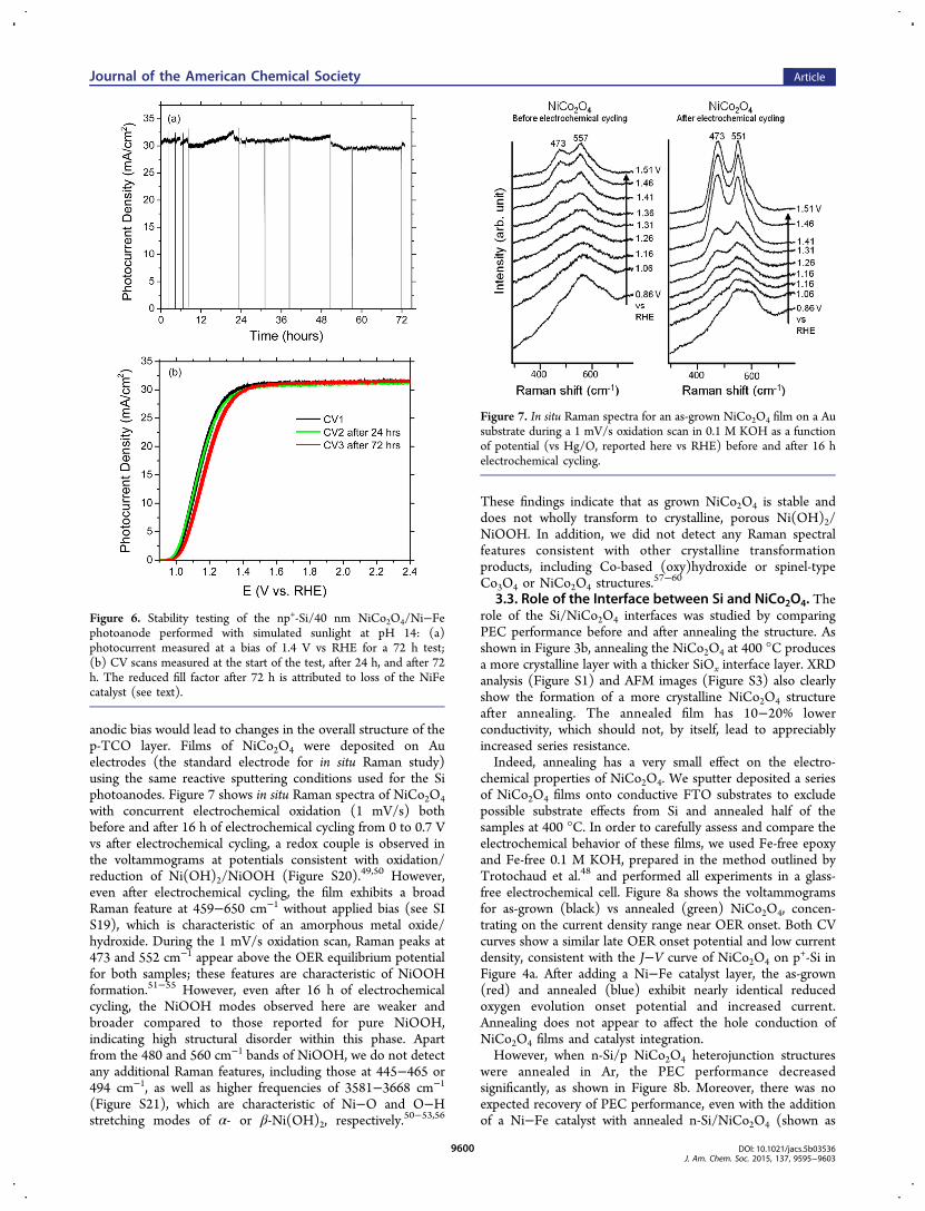
anodic bias would lead to changes in the overall structure of thep-TCO layer. Films of NiCo2O4 were deposited on Auelectrodes (the standard electrode for in situ Raman study)using the same reactive sputtering conditions used for the Siphotoanodes. Figure 7 shows in situ Raman spectra of NiCo2O4with concurrent electrochemical oxidation (1 mV/s) bothbefore and after 16 h of electrochemical cycling from 0 to 0.7 Vvs after electrochemical cycling, a redox couple is observed inthe voltammograms at potentials consistent with oxidation/reduction of Ni(OH)2/NiOOH (Figure S20).49,50 However,even after electrochemical cycling, the film exhibits a broadRaman feature at 459−650 cm−1 without applied bias (see SIS19), which is characteristic of an amorphous metal oxide/hydroxide. During the 1 mV/s oxidation scan, Raman peaks at473 and 552 cm−1 appear above the OER equilibrium potentialfor both samples; these features are characteristic of NiOOHformation.51−55 However, even after 16 h of electrochemicalcycling, the NiOOH modes observed here are weaker andbroader compared to those reported for pure NiOOH,indicating high structural disorder within this phase. Apartfrom the 480 and 560 cm−1 bands of NiOOH, we do not detectany additional Raman features, including those at 445−465 or494 cm−1, as well as higher frequencies of 3581−3668 cm−1
(Figure S21), which are characteristic of Ni−O and O−Hstretching modes of α- or β-Ni(OH)2, respectively.50−53,56
These findings indicate that as grown NiCo2O4 is stable anddoes not wholly transform to crystalline, porous Ni(OH)2/NiOOH. In addition, we did not detect any Raman spectralfeatures consistent with other crystalline transformationproducts, including Co-based (oxy)hydroxide or spinel-typeCo3O4 or NiCo2O4 structures.
57−60
3.3. Role of the Interface between Si and NiCo2O4. Therole of the Si/NiCo2O4 interfaces was studied by comparingPEC performance before and after annealing the structure. Asshown in Figure 3b, annealing the NiCo2O4 at 400 °C producesa more crystalline layer with a thicker SiOx interface layer. XRDanalysis (Figure S1) and AFM images (Figure S3) also clearlyshow the formation of a more crystalline NiCo2O4 structureafter annealing. The annealed film has 10−20% lowerconductivity, which should not, by itself, lead to appreciablyincreased series resistance.Indeed, annealing has a very small effect on the electro-
chemical properties of NiCo2O4. We sputter deposited a seriesof NiCo2O4 films onto conductive FTO substrates to excludepossible substrate effects from Si and annealed half of thesamples at 400 °C. In order to carefully assess and compare theelectrochemical behavior of these films, we used Fe-free epoxyand Fe-free 0.1 M KOH, prepared in the method outlined byTrotochaud et al.48 and performed all experiments in a glass-free electrochemical cell. Figure 8a shows the voltammogramsfor as-grown (black) vs annealed (green) NiCo2O4, concen-trating on the current density range near OER onset. Both CVcurves show a similar late OER onset potential and low currentdensity, consistent with the J−V curve of NiCo2O4 on p+-Si inFigure 4a. After adding a Ni−Fe catalyst layer, the as-grown(red) and annealed (blue) exhibit nearly identical reducedoxygen evolution onset potential and increased current.Annealing does not appear to affect the hole conduction ofNiCo2O4 films and catalyst integration.However, when n-Si/p NiCo2O4 heterojunction structures
were annealed in Ar, the PEC performance decreasedsignificantly, as shown in Figure 8b. Moreover, there was noexpected recovery of PEC performance, even with the additionof a Ni−Fe catalyst with annealed n-Si/NiCo2O4 (shown as
Figure 6. Stability testing of the np+-Si/40 nm NiCo2O4/Ni−Fephotoanode performed with simulated sunlight at pH 14: (a)photocurrent measured at a bias of 1.4 V vs RHE for a 72 h test;(b) CV scans measured at the start of the test, after 24 h, and after 72h. The reduced fill factor after 72 h is attributed to loss of the NiFecatalyst (see text).
Figure 7. In situ Raman spectra for an as-grown NiCo2O4 film on a Ausubstrate during a 1 mV/s oxidation scan in 0.1 M KOH as a functionof potential (vs Hg/O, reported here vs RHE) before and after 16 helectrochemical cycling.
Journal of the American Chemical Society Article
DOI: 10.1021/jacs.5b03536J. Am. Chem. Soc. 2015, 137, 9595−9603
9600
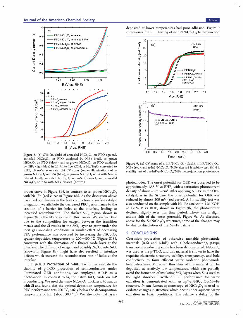
brown curve in Figure 8b), in contrast to as grown NiCo2O4with Ni−Fe (red curve in Figure 8b). As the discussion abovehas ruled out changes in the hole conduction or surface catalystintegration, we attribute the decreased PEC performance to thecreation of a barrier for holes at the interface, leading toincreased recombination. The thicker SiOx region shown inFigure 3b is the likely source of this barrier. We suspect thatdue to the competition for oxygen between the transitionmetals and the Si results in the SiOx layer to grow under theinert gas annealing conditions. A similar effect of decreasingPEC performance was observed by increasing the NiCo2O4sputter deposition temperature to 200−400 °C (Figure S18),consistent with the formation of a thicker oxide layer at theinterface. The diffusion of oxygen and possibly Ni/Co into SiOx(shown in Figure 3b) might have also resulted in interfacedefects which increase the recombination rate of holes at theinterface.3.3. p-TCO Protection of n-InP. To further evaluate the
viability of p-TCO protection of semiconductors underilluminated OER conditions, we employed n-InP as aphotoanode. In contrast to Si, the native InOx oxide on InPis conducting. We used the same NiCo2O4 thickness, 40 nm, aswith Si and found that the optimal deposition temperature forPEC performance was 200 °C, safely below the decompositiontemperature of InP (about 300 °C). We also note that layers
deposited at lower temperatures had poor adhesion. Figure 9summarizes the PEC testing of n-InP/NiCo2O4 heterojunction
photoanodes. The onset potential for OER was observed to beapproximately 1.55 V vs RHE, with a saturation photocurrentdensity of about 23 mA/cm2. After applying Ni−Fe as the OERcatalyst, as in the Si case, the onset potential for OER wasreduced by almost 200 mV (red curve). A 4 h stability test wasalso conducted on the sample with Ni−Fe catalyst in 1 M KOHat 1.624 V vs RHE, shown in Figure 9b; the photocurrentdeclined slightly over this time period. There was a slightanodic shift of the onset potential, Figure 9a. As discussedabove for the Si/NiCo2O4 structures, some of the changes maybe due to dissolution of the Ni−Fe catalyst.
5. CONCLUSIONSCorrosion protection of otherwise unstable photoanodematerials (n-Si and n-InP) with a hole-conducting, p-typetransparent conducting oxide has been demonstrated. NiCo2O4was used as the p-TCO, and this material is shown to have therequisite electronic structure, stability, transparency, and holeconductivity to form efficient water oxidation photoanodeheterostructures. Moreover, thin films of this material can bedeposited at relatively low temperatures, which can partiallyavoid the formation of insulating SiOx layers when Si is used asthe light absorber. Excellent PEC performance for wateroxidation is demonstrated with an np+-Si/NiCo2O4/Ni−Festructure. In situ Raman spectroscopy of NiCo2O4 is used toevaluate changes in structure which occur under aqueous wateroxidation in basic conditions. The relative stability of the
Figure 8. (a) CVs (in dark) of annealed NiCo2O4 on FTO (green),annealed NiCo2O4 on FTO catalyzed by NiFe (red), as grownNiCo2O4 on FTO (black), and as grown NiCo2O4 on FTO catalyzedby NiFe (light blue) in 0.1 M Fe-free KOH, vs Hg/HgO, converted toRHE, 10 mV/s scan rate. (b) CV scans (under illumination) of asgrown NiCo2O4 on n-Si (blue), as grown NiCo2O4 on Si with Ni−Fecatalyst (red), annealed NiCo2O4 on n-Si (orange), and annealedNiCo2O4 on n-Si with NiFe catalyst (brown).
Figure 9. (a) CV scans of n-InP/NiCo2O4 (black), n-InP/NiCo2O4/NiFe (red), and n-InP/NiCo2O4/NiFe after a 4 h stability test. (b) 4 hstability test of a n-InP/p-NiCo2O4/NiFe heterojunction photoanode.
Journal of the American Chemical Society Article
DOI: 10.1021/jacs.5b03536J. Am. Chem. Soc. 2015, 137, 9595−9603
9601

catalyst and the protection layer was confirmed by photo-current measurements and ICP-MS measurements of theelectrolyte following long-term testing for 72 h. The precisenature of the interface between the semiconductor and the p-TCO is shown to be crucial in achieving high PECperformance. For example, annealing n-Si/p-NiCo2O4 hetero-junction photoanodes produces only very small changes in theNiCo2O4 but significantly affects the interface structure, leadingto a decrease in performance. P-NiCo2O4 also forms a charge-separating heterojunction with n-InP and leads to stableoperation over several hours.
■ ASSOCIATED CONTENT*S Supporting InformationExperimental details; detailed characterization; photoelectro-chemical measurement details; supplemental stability data, andFaradaic efficiency; additional in situ Raman spectroscopy; XPSmeasurements; ab initio calculation of the work function;modeling of PEC data. The Supporting Information is availablefree of charge on the ACS Publications website at DOI:10.1021/jacs.5b03536.
■ AUTHOR INFORMATIONCorresponding Author*[email protected] authors declare no competing financial interest.
■ ACKNOWLEDGMENTSWe thank Raffaella Buonsanti for assistance with SEM imaging,Karl Walczak and Jeffery Beeman for Faradaic efficiencymeasurements and for processing np-Si wafers, and Prof. AliJavey’s group for providing n-InP wafers. We thank NCEM staffMarissa Libbee and Chengyu Song for generous help on TEMsample preparation and imaging. This material is based uponwork performed by the Joint Center for Artificial Photosyn-thesis, a DOE Energy Innovation Hub, supported through theOffice of Science of the U.S. Department of Energy underaward no. DE-SC0004993. Characterization work by R.W.R.was supported by the Bay Area Photovoltaic Consortium. Workat the National Center for Electron Microscopy and MolecularFoundry was supported by the Office of Science, Office of BasicEnergy Sciences, of the U.S. Department of Energy undercontract no. DE-AC02−05CH1123.
■ REFERENCES(1) Chu, S.; Majumdar, A. Nature 2012, 488 (7411), 294.(2) Nocera, D. G. Acc. Chem. Res. 2012, 45 (5), 767.(3) Turner, J. A. Science (Washington, DC, U. S.) 2004, 305 (5686),972.(4) Graves, C.; Ebbesen, S. D.; Mogensen, M.; Lackner, K. S.Renewable Sustainable Energy Rev. 2011, 15 (1), 1.(5) Khaselev, O.; Turner, J. A. Science (Washington, DC, U. S.) 1998,280 (5362), 425.(6) Brillet, J.; Cornuz, M.; Formal, F. Le; Yum, J.-H.; Gratzel, M.;Sivula, K. J. Mater. Res. 2010, 25 (01), 17.(7) Ronge, J.; Bosserez, T.; Martel, D.; Nervi, C.; Boarino, L.;Taulelle, F.; Decher, G.; Bordiga, S.; Martens, J. A. Chem. Soc. Rev.2014, 43, 7963.(8) Nielander, A. C.; Shaner, M. R.; Papadantonakis, K. M.; Francis,S. A.; Lewis, N. S. Energy Environ. Sci. 2015, 8 (1), 16.(9) Elsenberg, R.; Gray, H. B. Inorg. Chem. 2008, 47 (6), 1697.(10) Haussener, S.; Xiang, C.; Spurgeon, J. M.; Ardo, S.; Lewis, N. S.;Weber, A. Z. Energy Environ. Sci. 2012, 5 (12), 9922.
(11) Kohl, P. A.; Frank, S. N.; Bard, A. J. J. Electrochem. Soc. 1977,124 (2), 225.(12) Parkinson, B. Acc. Chem. Res. 1984, 17 (12), 431.(13) McKone, J. R.; Lewis, N. S.; Gray, H. B. Chem. Mater. 2014, 26(1), 407.(14) Liu, R.; Zheng, Z.; Spurgeon, J.; Yang, X. Energy Environ. Sci.2014, 7 (8), 2504.(15) Gerischer, H. J. Electroanal. Chem. Interfacial Electrochem. 1977,82 (1−2), 133.(16) Chen, S.; Wang, L.-W. Chem. Mater. 2012, 24 (18), 3659.(17) Kraft, A.; Gorig, B.; Heckner, K. H. Sol. Energy Mater. Sol. Cells1994, 32 (2), 151.(18) Seger, B.; Castelli, I. E.; Vesborg, P. C. K.; Jacobsen, K. W.;Hansen, O.; Chorkendorff, I. Energy Environ. Sci. 2014, 7 (8), 2397.(19) Sun, K.; Saadi, F. H.; Lichterman, M. F.; Hale, W. G.; Wang, H.-P.; Zhou, X.; Plymale, N. T.; Omelchenko, S. T.; He, J.-H.;Papadantonakis, K. M.; Brunschwig, B. S.; Lewis, N. S. Proc. Natl.Acad. Sci. U. S. A. 2015, 201423034.(20) Campet, G.; Puprichitkun, C.; Sun, Z. W. J. Electroanal. Chem.Interfacial Electrochem. 1989, 269 (2), 435.(21) Chen, Y. W.; Prange, J. D.; Duhnen, S.; Park, Y.; Gunji, M.;Chidsey, C. E. D.; McIntyre, P. C. Nat. Mater. 2011, 10 (7), 539.(22) Scheuermann, A. G.; Prange, J. D.; Gunji, M.; Chidsey, C. E. D.;McIntyre, P. C. Energy Environ. Sci. 2013, 6 (8), 2487.(23) Yang, X.; Liu, R.; Du, C.; Dai, P.; Zheng, Z.; Wang, D. ACSAppl. Mater. Interfaces 2014, 6 (15), 12005.(24) Sun, Z. W.; Campet, G. Mater. Sci. Eng., B 1990, 5 (4), 455.(25) Hu, S.; Shaner, M. R.; Beardslee, J. A.; Lichterman, M.;Brunschwig, B. S.; Lewis, N. S. Science (Washington, DC, U. S.) 2014,344 (6187), 1005.(26) Greiner, M. T.; Helander, M. G.; Tang, W. M.; Wang, Z. B.;Qiu, J.; Lu, Z. H. Nat. Mater. 2011, 11 (1), 76.(27) Fortunato, E.; Barquinha, P.; Martins, R. Adv. Mater. 2012, 24(22), 2945.(28) Ginley, D. S.; Bright, C. MRS Bull. 2000, 25 (08), 15.(29) Banerjee, A. N.; Chattopadhyay, K. K. Prog. Cryst. GrowthCharact. Mater. 2005, 50 (1−3), 52.(30) Stadler, A. Materials 2012, 5 (4), 661.(31) Fortunato, E.; Ginley, D.; Hosono, H.; Paine, D. C. MRS Bull.2007, 32, 242.(32) Yang, J.; Walczak, K.; Anzenberg, E.; Toma, F. M.; Yuan, G.;Beeman, J.; Schwartzberg, A.; Lin, Y.; Hettick, M.; Javey, A.; Ager, J.W.; Yano, J.; Frei, H.; Sharp, I. D. J. Am. Chem. Soc. 2014, 136 (17),6191.(33) Sun, K.; Shen, S.; Cheung, J. S.; Pang, X.; Park, N.; Zhou, J.; Hu,Y.; Sun, Z.; Noh, S. Y.; Riley, C. T.; Yu, P. K. L.; Jin, S.; Wang, D. Phys.Chem. Chem. Phys. 2014, 16 (10), 4612.(34) Mei, B.; Permyakova, A. A.; Frydendal, R.; Bae, D.; Pedersen,T.; Malacrida, P.; Hansen, O.; Stephens, I. E. L.; Vesborg, P. C. K.;Seger, B.; Chorkendorff, I. J. Phys. Chem. Lett. 2014, 5 (20), 3456.(35) Sun, K.; McDowell, M. T.; Nielander, A. C.; Hu, S.; Shaner, M.R.; Yang, F.; Brunschwig, B. S.; Lewis, N. S. J. Phys. Chem. Lett. 2015, 6(4), 592.(36) Singh, D. J. Electrochem. Soc. 1998, 145 (1), 116.(37) Yuan, Y. F.; Xia, X. H.; Wu, J. B.; Yang, J. L.; Chen, Y. B.; Guo,S. Y. Electrochim. Acta 2011, 56 (6), 2627.(38) Lin, F.; Boettcher, S. W. Nat. Mater. 2013, 13 (1), 81.(39) Windisch, C. F., Jr; Ferris, K. F.; Exarhos, G. J.; Sharma, S. K.Thin Solid Films 2002, 420−421, 89.(40) Alcantara, R.; Jaraba, M.; Lavela, P.; Tirado, J. L. Chem. Mater.2002, 14 (7), 2847.(41) Wei, T. Y.; Chen, C. H.; Chien, H. C.; Lu, S. Y.; Hu, C. C. Adv.Mater. 2010, 22 (3), 347.(42) Li, J.; Xiong, S.; Liu, Y.; Ju, Z.; Qian, Y. ACS Appl. Mater.Interfaces 2013, 5 (3), 981.(43) Kawazoe, H.; Yasukawa, M.; Hyodo, H.; Kurita, M.; Yanagi, H.;Hosono, H. Nature 1997, 389 (6654), 939.
Journal of the American Chemical Society Article
DOI: 10.1021/jacs.5b03536J. Am. Chem. Soc. 2015, 137, 9595−9603
9602

(44) Klein, A.; Korber, C.; Wachau, A.; Sauberlich, F.; Gassenbauer,Y.; Harvey, S. P.; Proffit, D. E.; Mason, T. O. Materials 2010, 3 (11),4892.(45) Hautier, G.; Miglio, A.; Ceder, G.; Rignanese, G.-M.; Gonze, X.Nat. Commun. 2013, 4, 2292.(46) Mills, T. J.; Lin, F.; Boettcher, S. W. Phys. Rev. Lett. 2014, 112(14), 148304.(47) Kenney, M. J.; Gong, M.; Li, Y.; Wu, J. Z.; Feng, J.; Lanza, M.;Dai, H. Science 2013, 342 (6160), 836.(48) Trotochaud, L.; Young, S. L.; Ranney, J. K.; Boettcher, S. W. J.Am. Chem. Soc. 2014, 136 (18), 6744.(49) Lyons, M. E. G.; Brandon, M. P. Int. J. Electrochem. Sci. 2008, 3(12), 1386.(50) Kostecki, R. J. Electrochem. Soc. 1997, 144 (2), 485.(51) Cornilsen, B. C.; Karjala, P. J.; Loyselle, P. L. J. Power Sources1988, 22, 351.(52) Desilvestro, J. J. Electrochem. Soc. 1988, 135 (4), 885.(53) Johnston, C.; Graves, P. R. Appl. Spectrosc. 1990, 44 (1), 105.(54) Yeo, B. S.; Bell, A. T. J. Phys. Chem. C 2012, 116 (15), 8394.(55) Louie, M. W.; Bell, A. T. J. Am. Chem. Soc. 2013, 135 (33),12329.(56) Bernard, M. C.; Bernard, P.; Keddam, M.; Senyarich, S.;Takenouti, H. Electrochim. Acta 1996, 41 (1), 91.(57) Pauporte, T.; Mendoza, L.; Cassir, M.; Bernard, M. C.; Chivot, J.J. Electrochem. Soc. 2005, 152 (2), C49.(58) Tang, C. W.; Wang, C. Bin; Chien, S. H. Thermochim. Acta2008, 473 (1−2), 68.(59) Yang, J.; Liu, H.; Martens, W. N.; Frost, R. L. J. Phys. Chem. C2010, 114 (1), 111.(60) Iliev, M. N.; Silwal, P.; Loukya, B.; Datta, R.; Kim, D. H.;Todorov, N. D.; Pachauri, N.; Gupta, A. J. Appl. Phys. 2013, 114 (3),033514.
Journal of the American Chemical Society Article
DOI: 10.1021/jacs.5b03536J. Am. Chem. Soc. 2015, 137, 9595−9603
9603


![Entropy Generation Minimization for Reverse Water Gas ... · Bak et al. [37], Chen et al. [38] and Wang et al. [39] investigated the optimal configurations of a generalized consecutive](https://img.pdfslide.us/doc/110x75/5ec2f7b6850bc463b84f6fa0/entropy-generation-minimization-for-reverse-water-gas-bak-et-al-37-chen.jpg)


![arXiv:1810.02334v1 [cs.LG] 4 Oct 2018 · 2018-10-05 · resentations (Reed et al., 2014; Cheung et al., 2015; Chen et al., 2016) or fine-tuning a learned model (Erhan et al., 2010)](https://img.pdfslide.us/doc/110x75/5f7e78a97926323b3347eb12/arxiv181002334v1-cslg-4-oct-2018-2018-10-05-resentations-reed-et-al-2014.jpg)