Embed Size (px)
Citation preview
a ,
CHEMICAL MECHANICAL POLISHING: AN ENABLING FABRICATION PROCESS FOR SURFACE MICROMACHINING TECHNOLOGIES
Jeffry J. Sniegowski Sandia National Laboratories
Albuquerque, NM 87185-1080 http://www.mdl. sandia.gov/Micromachine
MS-1080, P.O. BOX 5800
ABSTRACT
Chemical-Mechanical-Polishing (CMP), first used as a planarization technology in the manufacture of multi-level metal interconnects for high-density Integrated Circuits (IC), is readily adapted as an enabling technology in MicroElectroMechanical Systems (MEMS) fabrication, particularly polysilicon surface micromachining . We have demonstrated that CMP enhances the design and manufacturability of MEMS devices by eliminating several photolithographic definition and film etch issues generated by severe topography. In addition, CMP planarization readily allows multi-level polysilicon structures comprised of 4- or more levels of polysilicon, eliminates design compromise generated by non-planar topography, and provides an avenue for integrating different process technologies. A recent investigation has also shown that CMP is a valuable tool for assuring acceptable optical flatness of micro-optical components such as micromirrors. Examples of these enhancements include: an extension of polysilicon surface-micromachining fabrication to a 5-level technology, a method of monolithic integration of electronics and MEMS, and optically flat micromirrors.
INTRODUCTION
Earlier reports cover, in greater detail, the benefits of wafer planarization by chemical-mechanical-polishing (CMP) for MicroElectroMechanical Systems (MEMS) fabrication (1). This paper provides an overview of these benefits and discusses the latest advancements to polysilicon micromachining enabled by CMP planarization. Polysilicon surface-micromachining, because it is extensively based on integrated circuit (IC) fabrication techniques and equipment sets, lends itself readily to adaptation of CMP for planarization of excess surface topography. First, a brief description of CMP process technology followed by a cursory description of polysilicon surface micromachining clearly illustrates why CMP is compatible with and beneficial to surface micromachining technology. Next, a brief example illustrates how CMP enhances the manufacturability of a standard, non-planarized surface micromachining process while the final section discusses new process and design directions enabled through the use of CMP.

DISCLAIMER
This report was prepared as an account of work sponsored by an agency of the United States Government. Neither the United States Government nor any agency thereof, nor any of their employees, makes any warranty, express or implied, or assumes any legal liability or responsibility for the accuracy, completeness, or use- fulness of any information, apparatus, product, or process disclosed, or represents that its use would not infringe privately owned rights. Reference herein to any spe- cific commercial product, process, or service by trade name, trademark, manufac- turer, or otherwise does not nccessarily constitute or imply its endorsement, recom- mendktion, or favoring by the United States Government or any agency thereof. The views and opinions of authors expressed herein do not necessarily state or reflcct thost of the United States Government or any agency thereof.

DISCLAIMER
Portions of this document may be illegible in electronic image products. Images are produced from the best available original document -
CHEMICAL MECHANICAL POLISHING
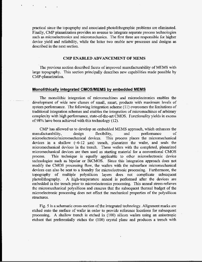
CMP processes produce both global and local planarization through relatively simple and quick processing. Figure 1 illustrates the CMP process in which an oxide surface is planarized by rotating a wafer under pressure against a polishing pad in the presence of a silica-based alkaline slurry. The theory of oxide polishing is not well understood, however, it is generally accepted that the alkaline chemistry hydrolyzes the oxide surface and sub-surface, which weakens the Si02 bond structure (2). The mechanical energy
imparted to the abrasive slurry particle through pressure and rotation causes high features to erode at a faster rate than low features, thereby planarizing the surface over time. For the particular results shown here, a colloidal-fumed silica slurry (Cabot SS-12) and a polyurethane pad (Rode1 IC 1000/Suba IV) are used.
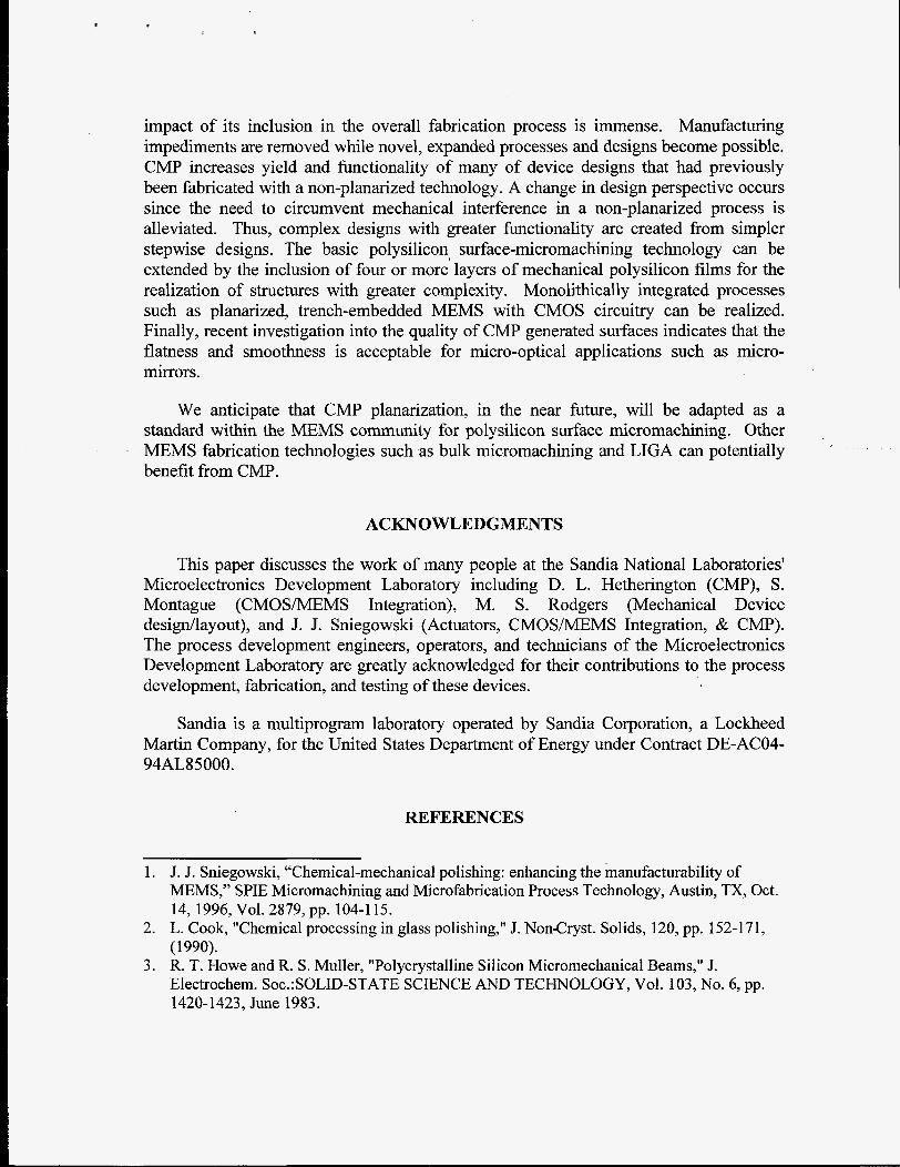
One of the main differences between planarizing inter-level dielectric materials used in ULSI interconnect technology and planarizing sacrificial oxide material used in MEMS technology is the large step heights (2-8 pm vs. 0.8 pm) associated with polysilicon surface micromachined MEMS. These large step heights present a challenge to any planarization strategy. Figure 2 shows the surface topography of single level polysilicon structure prior to CMP (2a) and after the CMP process (2b). As seen from the figure, CMP does an excellent job of removing the - 2 pm step height and planarizing the oxide surface.
CMP ENHANCED MANUFACTURABLILITY
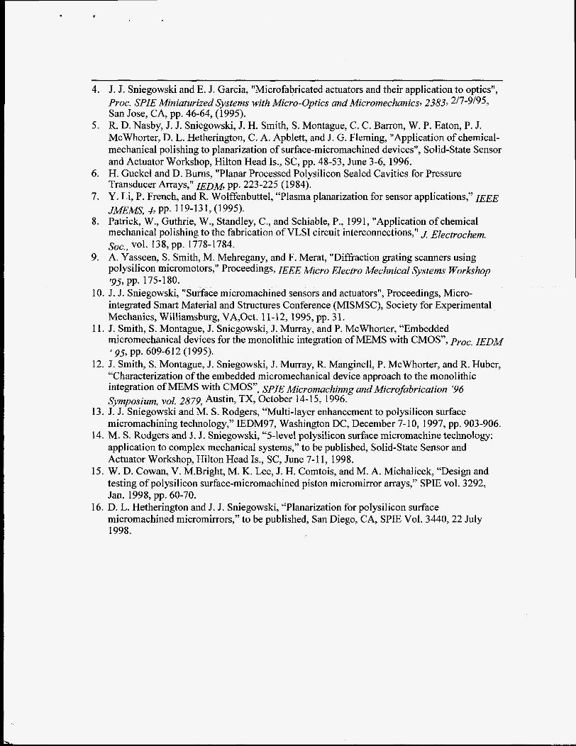
MEMS device fabrication technologies, and in particular polysilicon surface micromachining (3,4), have been plagued by process issues generated by severe vertical topography introduced by the repetitive deposition and etching of multiple films. Polysilicon surface micromachining readily adapts to the inclusion of CMP and clearly illustrates the benefits of CMP. Surface micromachining uses planar fabrication techniques and films common to the microelectronic circuit fabrication industry to manufacture micromechanical devices. The standard building-block process consists of depositing and photolithographically patterning alternate layers of low-stress polycrystalline silicon and sacrificial silicon dioxide. The result is a construction system consisting of one layer of polysilicon which provides electrical interconnection and one or more independent layers of mechanical polysilicon which can be used to form mechanical elements ranging from simple cantilevered beams to complex systems of springs, linkages, mass elements and joints. At the completion of the process, the sacrificial layers, as their name suggests, are selectively etched away in hydrofluoric acid (HF), which leaves the free-standing polysilicon layers. Figure 3 illustrates the additive nature of polysilicon surface micromachining and clearly displays the vertical topography that arises in a non-planarized process. This topography can produce mechanical interference between moving parts, and complicates subsequent process steps.
The mechanical interference arises when an upper layer of polysilicon must pass over the edge of a previously etched lower layer as seen in Fig. 3 at point B. This feature is due to the conformal deposition of the polysilicon film. The bottom of the protrusion is clearly seen to be below the level of the top of the element A. This protrusion would prevent a 90-degree rotation of the joint due to interference with the linkage at level A, which extends into the background. Link/gear interference can be circumvented by the microengine design; however, this often compromises or prevents potential designs. The preferred solution is the planarization of the surfaces before subsequent deposition of additional films as illustrated in the CMP-planarized joint in Fig. 4.
In addition to potential design constraints, two significant process difficulties arise from severe topography. The first results from the use of highly anisotropic plasma etch processes for the definition of the polysilicon layers. The anisotropy is necessary to obtain the desired vertical sidewalls of the polysilicon structures. However, the very anisotropy of this etch prevents removal of the polysilicon layer from along the edge of a step. This produces long slivers of polysilicon, often referred to as stringers, along these edges. The stringers can produce mechanical interference or even electrical shorting. Secondly, photolithographic definition of subsequent layers becomes problematic over severe topography. Photoresist, the photosensitive polymeric coating used to transfer the design into the physical films, becomes difficult to apply, expose, and develop, leading to loss of resolution and definition. Removal of these difficulties through the use of CMP aids manufacturability by reducing or eliminating photolithography reworks.
Thus, the addition of CMP planarization to polysilicon surface micromachining technology eliminates significant issues that promotes simpler and higher yielding manufacture (5). Researchers in the MEMS community have investigated techniques for planarization, other than CMP. For example, researchers at University of Wisconsin have demonstrated locally-planarized surface-micromachined pressure sensors produced in a double LOCOS process (6); while the use of plasma planarization has been demonstrated on MEMS devices by researchers at Delft (7).
Although these planarization techniques have yielded improvement in the manufacturability of MEMS devices through local planarization, CMP provides a higher quality of both local and global planarization in a manufacturing environment as has been established through its use in sub-micron circuit technology (8). While Yasseen et a1 used a simple polishing technique to enhance the reflectivity of polysilicon by smoothing its surface (9), the first general use of CMP planarization in MEMS was reported by Sniegowski (10) in the application of a three-level polysilicon process for the microengine.
The benefits of CMP for surface-micromachining are four-fold. It eliminates the potential mechanical interference problem. It eliminates the artifact of anisotropic etching of conformal polysilicon films over edges, i.e. stringers, since there are no edges on a planar surface. Thirdly, the extension to four or more levels of polysilicon becomes
practical since the topography and associated photolithographic problems are eliminated. Finally, CMP planarization provides an avenue to integrate separate process technologies such as microelectronics and micromechanics. The first three are responsible for higher device yield and reliability, while the latter two enable new processes and designs as described in the next section.
CMP ENABLED ADVANCEMENT OF MEMS
The previous section described facets of improved manufacturability of MEMS with large topography. This section principally describes new capabilities made possible by CMP-planarization.
Monolithically integrated CMOSIMEMS by embedded MEMS
The monolithic integration of micromachines and microelectronics enables the development of wide new classes of small, smart, products with maximum levels of system performance. The following integration scheme (1 1) overcomes the limitations of traditional integration schemes and enables the integration of micromachines of arbitrary complexity with high performance, state-of-the-art CMOS. Functionality yields in excess of 98% have been achieved with this technology (1 2).
CMP has allowed us to develop an embedded MEMS approach, which enhances the
microelectronic/micromechanical devices. This process places the micromechanical devices in a shallow (-6-12 pm) trench, planarizes the wafer, and seals the micromechanical devices in the trench. These wafers with the completed, planarized micromechanical devices are then used as starting material for a conventional CMOS process. This technique is equally applicable to other microelectronic device technologies such as bipolar or BiCMOS. Since this integration approach does not modify the CMOS processing flow, the wafers with the subsurface micromechanical devices can also be sent to a foundry for microelectronic processing. Furthermore, the topography of multiple polysilicon layers does not complicate subsequent photolithography. A high-temperature anneal is performed after the devices are embedded in the trench prior to microelectronics processing. This anneal stress-relieves the micromechanical polysilicon and ensures that the subsequent thermal budget of the microelectronic processing does not affect the mechanical properties of the polysilicon structures.
manufacturability , design flexibility, and performance of
Fig. 5 is a schematic cross-section of the integrated technology. Alignment marks are etched onto the surface of wafer in order to provide reference locations for subsequent processing. A shallow trench is etched in (100) silicon wafers using an anisotropic etchant that preferentially etches the (100) crystal plane and produces a trench with

sidewalls having a slope of 54.7" relative to the surface. subsequent photo patterning within the wells.
This slope aids in the
The alignment marks from the top surface of the wafer are used as references to generate another set of alignment marks on the bottom surface of the trench. This approach is used to optimize level-to-level registration and resolution of features within the trench. Feature sizes with critical dimensions as small as 0.8 pm, the limit of g-line lithography, were successfully defined within the trench.
A silicon nitride film is deposited to form a dielectric layer on the bottom of the trench. Sacrificial oxide and multiple layers of polysilicon are then deposited and patterned in a standard surface micromachining process. Polysilicon studs provide contact between the micromechanical devices and the CMOS devices; the depth of the trench is sized so that the top of the polysilicon stud lies just below the top of the planarized trench. The shallow trenches are then filled with a series of oxide depositions optimized to eliminate void formation in high-aspect-ratio structures. The wafer is subsequently planarized with chemical-mechanical polishing using the silicon nitride film as a polish stop. The silicon nitride is subsequently removed, and the entire structure is annealed to relieve stress in the structural polysilicon and sealed with a silicon nitride cap. At this point, conventional CMOS processing is performed. The backend of the process requires an additional step to open the nitride cap over the micromechanical layer prior to release of the micromechanical structures. Photoresist is used as a protection layer over the exposed bond pads during the release process.
The modularity of the process allows changes to be made to either the micromechanical process or the microelectronic process without affecting the other process. A planarized wafer with the embedded MEMS can serve as starting material for a conventional microelectronics foundry service since the technology does not require significant modifications of standard microelectronic fabrication processes.
SUMMIT-V: a five-level polysilicon surface micromachining technology
Polysilicon surface-micromachining is one technology that can greatly benefit by increasing the number of layers currently available for design. The complexity of the devices that can be fabricated in a polysilicon surface-micromachining technology scales super-linearly with the number of layers, analogous to design with multiple integrated circuit (IC) metalization layers. This 5-level process allows the design of extremely complex micromechanical functions, with concomitant increase in device reliability and robustness (1 3,14).
The continued inclusion of advanced IC process techniques in the manufacturing process for micromechanical devices was essential to the 5-level process development. For example, consistent yield and high-reliability with 3 (or greater)-level polysilicon surface-micromachining requires planarization of surface topography. In fact, 5-layers

would be virtually impossible without planarization. CMP has provided the means to overcome surface topography, historically the primary impediment to extension to additional levels. In addition, film optimization for mechanical properties allows the fabrication of structures with millimeter span and micrometer dimension features. The addition of independent layers available to the designer not only impacts the overall complexity of the devices, but also impacts their function, reliability, and robustness. For example, an accelerometer with a spring and proof mass can be realized in a single level. However, the additional levels provide signal transduction, protective stops for mechanical over-stress, and force rebalance mechanisms. In another example, complex machinery consisting of actuators with rotating elements on movable platforms can be realized only if sufficient independent design levels are present as illustrated in Fig. 6.
A recent application of CMP: micro-optics
The work of Yasseen et a1 demonstrated that the surface roughness of as-deposited polysilicon could be polished to an optical smoothness for polysilicon micro-mirrors through the use of a simple polishing technique (9). Recent work by Cowan et a1 with micro-mirrors for adaptive optics built in the Sandia SUMMiT process (1 5) illustrated a need to further investigate CMP to obtain acceptable optical flatness. Acceptable flatness being defined as <hllO, where h, in this case, is the 632.8nm HeNe laser wavelength. In Cowan's devices, the baseline process flow of the original SUMMiT process was developed to provide flatness acceptable for mechanical applications. Since -that discovery, we have been investigating the SUMMiT process flow to eliminate topography print-through from underlying layers for optical device applications. Print- through is defined as the steps seen in the upper polysilicon surface from underlying layers. On Cowan's devices, the print-through was on the order of 160-170 nm, which does not cause mechanical or manufacturing interference but can still affect optical elements. Fig. 7 illustrates a typical profile of the underlying oxide both pre- and post CMP. One sees that the severe topography of 2.5 um, which can lead to mechanical and manufacturing interference, is eliminated but that a small (< 0.1 um) residual remains.
Hetherington recently reported details of those experiments (16). The results, to date, are very promising and clearly indicate that insertion of CMP at the correct point in fabrication can minimize print-through to an optically acceptable flatness. In summary, the results indicate that the print-through can be reduced to < 22 nm, which is acceptable for adaptive optics in the visible range. Further work is in progress to evaluate surface smoothness and flatness of the chemical-mechanical polished polysilicon surfaces.
CONCLUSIONS
Chemical-mechanical polishing, once it is set-up and developed in a fabrication line, can be readily adapted as a planarization technique for use in polysilicon surface micromachining technology. Although planarization is a conceptually "simple" step, the
impact of its inclusion in the overall fabrication process is immense. Manufacturing impediments are removed while novel, expanded processes and designs become possible. CMP increases yield and functionality of many of device designs that had previously been fabricated with a non-planarized technology. A change in design perspective occurs since the need to circumvent mechanical interference in a non-planarized process is alleviated. Thus, complex designs with greater functionality are created from simpler stepwise designs. The basic polysilicon surface-micromachining technology can be extended by the inclusion of four or more layers of mechanical polysilicon films for the realization of structures with greater complexity. Monolithically integrated processes such as planarized, trench-embedded MEMS with CMOS circuitry can be realized. Finally, recent investigation into the quality of CMP generated surfaces indicates that the flatness and smoothness is acceptable for micro-optical applications such as micro- mirrors.
We anticipate that CMP planarization, in the near hture, will be adapted as a standard within the MEMS community for polysilicon surface micromachining. Other MEMS fabrication technologies such as bulk micromachining and LIGA can potentially benefit from CMP.
ACKNOWLEDGMENTS
This paper discusses the work of many people at the Sandia National Laboratories' Microelectronics Development Laboratory including D. L. Hetherington (CMP), S. Montague (CMOSMEMS Integration), M. S. Rodgers (Mechanical Device desigdlayout), and J. J. Sniegowski (Actuators, CMOS/MEMS Integration, & CMP). The process development engineers, operators, and technicians of the Microelectronics Development Laboratory are greatly acknowledged for their contributions to the process development, fabrication, and testing of these devices.
Sandia is a multiprogram laboratory operated by Sandia Corporation, a Lockheed Martin Company, for the United States Department of Energy under Contract DE-AC04- 94AL85 000.
REFERENCES
1. J. J. Sniegowski, "Chemical-mechanical polishing: enhancing the manufacturability of MEMS," SPIE Micromachining and Microfabrication Process Technology, Austin, TX, Oct.
2. L. Cook, "Chemical processing in glass polishing," J. NonCryst. Solids, 120, pp. 152-171, (1990).
3. R. T. Howe and R. S. Muller, "Polycrystalline Silicon Micromechanical Beams," J. Electrochem. Soc.:SOLID-STATE SCIENCE AND TECHNOLOGY, Vol. 103, No. 6, pp. 1420-1423, June 1983.
14, 1996, VOI. 2879, pp. 104-1 15.
4. J. J. Sniegowski and E. J. Garcia, “Microfabricated actuators and their application to optics”, Proc. SPIE Miniaturized Systems with Micro-Optics and Micromechanics, 2383, 2/7-9195, San Jose, CA, pp. 46-64, (1 995).
5. R. D. Nasby, J. J. Sniegowski, J. H. Smith, S. Montague, C. C. Barron, W. P. Eaton, P. J. McWhorter, D. L. Hetherington, C. A. Apblett, and J. G. Fleming, “Application of chemical- mechanical polishing to planarization of surface-micromachined devices”, Solid-state Sensor and Actuator Workshop, Hilton Head Is., SC, pp. 48-53, June 3-6, 1996.
6. H. Guckel and D. Burns, “Planar Processed Polysilicon Sealed Cavities for Pressure Transducer Arrays,“ IEDM, pp. 223-225 (1984).
7. Y. Li, P. French, and R. Wolffenbuttel, “Plasma planarization for sensor applications,” I - E E JMEMS, 4, PP. 119-131, (1995).
8. Patrick, W., Guthrie, W., Standley, C., and Schiable, P., 1991, ”Application of chemical mechanical polishing to the fabrication of VLSI circuit interconnections,” J. Electrochem.
9. A. Yasseen, S. Smith, M. Mehregany, and F. Merat, “Diffraction grating scanners using PolYsiliCon micromotors7” Proceedings, IEEE Micro Electro Mechnical Systems Workshop
sot., V O ~ . 138, pp. 1778-1784.
’95, pp. 175-180. 10. J. J. Sniegowski, “Surface micromachined sensors and actuators”, Proceedings, Micro-
integrated Smart Material and Structures Conference (MISMSC), Society for Experimental Mechanics, Williamsburg, VA,Oct. 11-12, 1995, pp. 31.
micromechanical devices for the monolithic integration of MEMS with CMOS”, proc, IEDM
12. J. Smith, S. Montague, J. Sniegowski, J. Murray, R. Manginell, P. McWhorter, and R. Huber,
1 1 . J. Smith, S. Montague, J. Sniegowski, J. Murray, and P. McWhorter, “Embedded
95, pp. 609-612 (1995).
“Characterization of the embedded micromechanical device approach to the monolithic integration of MEMS with CMOS”, SPIE Micromachinng and Microfabrication ‘96 symposium, vel. 2879, Austin, TX, October 14-15, 1996.
13. J. J. Sniegowski and M. S. Rodgers, “Multi-layer enhancement to polysilicon surface
14. M. S. Rodgers and J. J. Sniegowski, “5-level polysilicon surface micromachine technology: micromachining technology,’’ IEDM97, Washington DC, December 7- 10, 1997, pp. 903-906.
application to complex mechanical systems,’’ to be published, Solid-state Sensor and Actuator Workshop, Hilton Head Is., SC, June 7-1 1, 1998.
15. W. D. Cowan, V. M.Bright, M. K. Lee, J. H. Comtois, and M. A. Michalicek, “Design and testing of polysilicon surface-micromachined piston micromirror arrays,” SPIE vol. 3292, Jan. 1998, pp. 60-70.
micromachined micromirrors,” to be published, San Diego, CA, SPIE Vol. 3440,22 July 1998.
16. D. L. Hetherington and J. J. Sniegowski, “Planarization for polysilicon surface
.
Down Force Rotation
- Carrier c Carrier insert
Fig. 1 Schematic representation of CMP process in which an oxide surface is planarized by rotating the wafer under pressure against a polishing pad in the presence of a silica-based alkaline slurry.
lanar surface
Fig. 2 A SEM cross-section in 2a of a partially-fabricated micromachine illustraks the uneven, severe topography before CMP planarization. Fig. 2b is a cross-section of a partially-fabricated micromachine after CMP planarization. Note the planarity of the upper oxide surface.
Fig. 3 Focused Ion Beam (FIB) milled cross-section of a mechanical joint formed in a three- layer polysilicon surface micromachining technology. The final mechanical polysilicon film is the upper light-colored film. It illustrates the topography and the interference artifacts generated (arrows B & C) by the previous film steps (arrow A). The film thicknesses are on the order of 2pm for both the mechanical polysilicon films and the sacrificial silicon dioxide films.
I
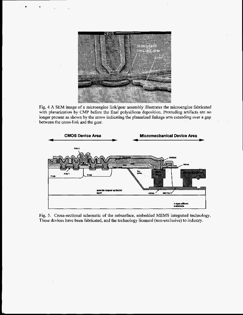
Fig. 4 A SEM image of a microengine link/gear assembly illustrates the microengine fabricated with planarization by CMP before the final polysilicon deposition. Protruding artifacts are no longer present as shown by the arrow indicating the planarized linkage arm extending over a gap between the cross-link and the gear.
CMOS Device Area Micromechanical Device Area 4 e 4 *
I Nlbld. ' m poh 0' I
Fig. 5. Cross-sectional schematic of the subsurface, embedded MEMS integrated technology. These devices have been fabricated, and the technology licensed (non-exclusive) to industry.
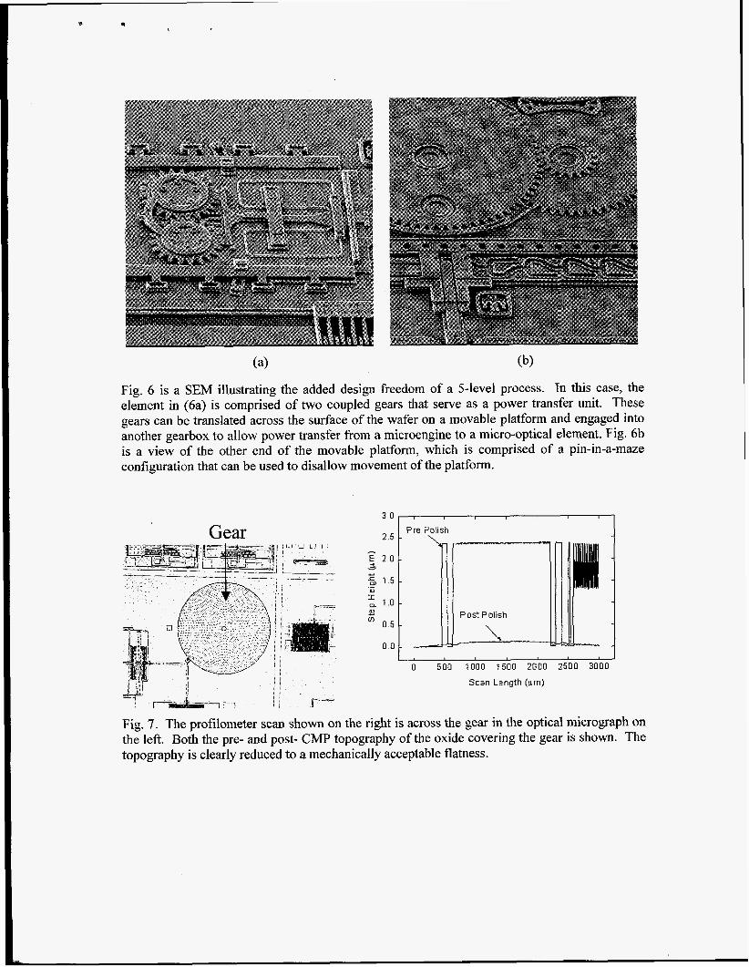
Fig. 6 is a SEM illustrating the added design freedom of a 5-level process. In this case, the element in (6a) is comprised of two coupled gears that serve as a power transfer unit. These gears can be translated across the surface of the wafer on a movable platform and engaged into another gearbox to allow power transfer from a microengine to a micro-optical element. Fig. 6b is a view of the other end of the movable platform, which is comprised of a pin-in-a-maze configuration that can be used to disallow movement of the platform.
3 0 , , Pre Polish
2 5 - Gear
3
? Y
1 5 - - Post Polish 0
p -A
I
I b ’
0 0
0 500 1000 1500 2000 2500 3000
Scan Length (prn)
ii’ =-
Fig. 7. The profilometer scan shown on the right is across the gear in the optical micrograph on the left. Both the pre- and post- CMP topography of the oxide covering the gear is shown. The topography is clearly reduced to a mechanically acceptable flatness.