Embed Size (px)
Citation preview
Chemical Engineering Journal 142 (2008) 337–343
Contents lists available at ScienceDirect
Chemical Engineering Journal
journa l homepage: www.e lsev ier .com/ locate /ce j
Synthesis of two-dimensional ZnO nanopellets by pyrolysis of zinc oleate
W.S. Chiua, P.S. Khiewa,∗, D. Isaa, M. Clokea, S. Radimanb, R. Abd-Shukorb, M.H. Abdullahb, N.M. Huangb
a Faculty of Engineering, University of Nottingham Malaysia Campus, Jln Broga 43500, Semenyih, Selangor Darul Ehsan, Malaysiab School of Applied Physics, Faculty of Science & Technology (UKM), Universiti Kebangsaan Malaysia, 43600 Bangi, Selangor Darul Ehsan, Malaysia
a r t i c l e i n f o
Article history:Received 17 March 2008Received in revised form 23 April 2008Accepted 25 April 2008
Keywords:Characterization
a b s t r a c t
We report the non-hydrolytic solution phase synthesis of two-dimensional zinc oxide (ZnO) nanopel-lets by using self-made organometallic compound (zinc (II) oleate, Zn(C18H33O2)2) as single precursor.Zn(C18H33O2)2 is prepared by ion exchange reaction between non-toxic fatty acid (palm oil extract) andion Zn2+. The controlling process of thermal pyrolysis of precursor is carried out under inert argon (Ar)atmosphere. This technique is very effective and reproducible in controlling the shape of ZnO semicon-ductor nanostructures. The as-synthesized ZnO nanocrystals are found in two-dimensionally well-faceted
Crystal morphologyGrowth from solutionZinc oxideS
triangular and hexagonal thin pellet structures. Transmission electron micrograph(s) (TEM) show that themorphologies of ZnO nanopellets can be controlled by annealing duration. X-ray powder diffraction pat-terns reveal that all the peaks of ZnO nanopellets can be well indexed with standard hexagonal phase of
1
segadaicutqtaegu
detds
qbcvdtrtss
imiFslbgio
1d
emiconducting II–VI materials ZnO crystal structure.
. Introduction
Nanomaterials have received considerable attention from thecientific and engineering communities due to their novel prop-rties and various techniques have been employed to control theireometrical factors including size and shape. The purposes of thesessiduous efforts are to tune and exploit various anomalous shapesependent properties of nanomaterials. For instances, Wang etl. have observed unusual polarization anisotropy properties ofndium phosphide (InP) nanowires synthesized by laser-assistedatalytic growth and these nanowires have subsequently beentilized in fabrication of polarization-sensitive nanoscale pho-odetectors [1]. In addition, Zhong et al. have prepared highuality single crystal p-type gallium nitride (GaN) semiconduc-or nanowires by chemical vapor deposition (CVD) and technicallypplied it as nanoscale UV–blue LEDs [2]. Further to this, Hahmt al. have also reported p-type silicon nanowires that have beenrown by CVD and they chemically incorporated these materials inltra-sensitive electrical detection of DNA [3].
Nowadays, the innovative application of nanomaterials in theesign of electronic devices is massively dependent on the congru-
nt electronic properties of the selected nanomaterials. However,he electronic property is highly influenced by the structuralimension of the nanomaterials. Regarding to the structural dimen-ion of nanomaterials, for 1D semiconductor nanostructures, the∗ Corresponding author. Tel.: +60 3 89248179; fax: +60 3 89248017.E-mail address: [email protected] (P.S. Khiew).
pitsaict
385-8947/$ – see front matter © 2008 Elsevier B.V. All rights reserved.oi:10.1016/j.cej.2008.04.034
© 2008 Elsevier B.V. All rights reserved.
uasi-continuous density of states exhibits singularities near theand edges followed by exponentially decay while that of 2D semi-onductor nanostructures is partially discrete [4,5]. Substantialariation in electrical and optical properties in accordance to theimensional changes can be observed when the particular elec-ronic energy gap exceeds the thermal energy. Some examples ofemarkable 2D quantizes effects are integer and fractional quan-um hall effects [6–9]. Therefore, a routine method in preparing 2Demiconductor nanostructures should be developed to unravel thehape-guiding effects.
Generally, there are two renowned synthetic approaches usedn preparing desirable semiconductor nanostructures of the nano-
aterials for the application purposes. One synthetic approachs gas-phase synthesis while another is solution-phase synthesis.or most of 1D nanowires which prepared by gas-phase synthe-is, the major limitation subjected to this synthetic approach isow yield and consuming large amount of thermal energy. Thus, itecomes an obstacle for large-scale production. In contrast to thisas-phase synthesis, the problem mentioned above can be solvedn solution-phase synthesis. Additionally, solution-phase synthesisffers a more economical route, high throughput and large-scaleroduction of high quality nanostructures that are monodisperse
n shape and size [10–12]. For example, by scrupulously controllinghe chemical reaction in solution-phase synthesis, Law et al. have
uccessfully boosted the aspect ratio of ZnO nanowires above 125nd tremendously increased the yield. Furthermore, this topologys found to improve the quantum efficiency of dye-sensitized solarells (DSCs) in the red region of the spectrum in order to attainhe full sun efficiency up to 1.5% [13]. Thus, solution-phase syn-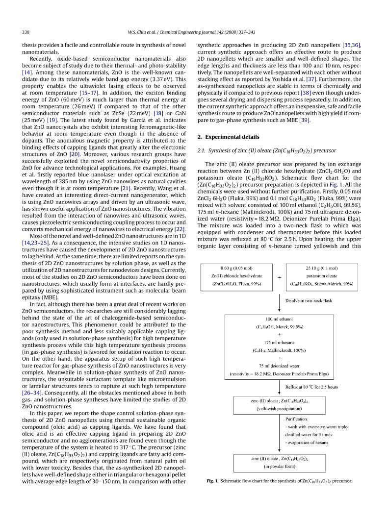
3 neerin
tn
b[dpaers(tbdbssZewehihrcc
[tttumnpe
Zbtpas(Otcto[gZ
tcost(pwlw
sc2etsapgtsp
2
2
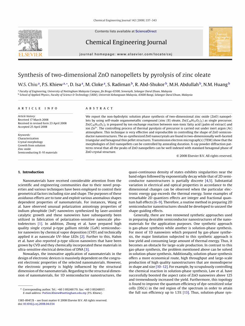
rp(cZm1iThe mixture was loaded into a two-neck flask to which wasequipped with condenser and thermometer before this loadedmixture was refluxed at 80 ◦C for 2.5 h. Upon heating, the upperorganic layer consisting of n-hexane turned yellowish and this
38 W.S. Chiu et al. / Chemical Engi
hesis provides a facile and controllable route in synthesis of novelanomaterials.
Recently, oxide-based semiconductor nanomaterials alsoecome subject of study due to their thermal- and photo-stability14]. Among these nanomaterials, ZnO is the well-known can-idate due to its relatively wide band gap energy (3.37 eV). Thisroperty enables the ultraviolet lasing effects to be observedt room temperature [15–17]. In addition, the exciton bindingnergy of ZnO (60 meV) is much larger than thermal energy atoom temperature (26 meV) if compared to that of the otheremiconductor materials such as ZnSe (22 meV) [18] or GaN25 meV) [19]. The latest study found by Garcia et al. indicateshat ZnO nanocrystals also exhibit interesting ferromagnetic-likeehavior at room temperature even though in the absence ofopants. The anomalous magnetic property is attributed to theinding effects of capping ligands that greatly alter the electronictructures of ZnO [20]. Moreover, various research groups haveuccessfully exploited the novel semiconductivity properties ofnO for advance technological applications. For examples, Huangt al. firstly reported blue nanolaser under optical excitation atavelength of 385 nm by using ZnO nanowires as natural cavities
ven though it is at room temperature [21]. Recently, Wang et al.ave created an interesting direct-current nanogenerator, which
s using ZnO nanowires arrays and driven by an ultrasonic wave,as shown useful application of ZnO nanostructures. The vibrationesulted from the interaction of nanowires and ultrasonic waves,auses piezoelectric semiconducting coupling process to occur andonverts mechanical energy of nanowires to electrical energy [22].
Most of the novel and well-defined ZnO nanostructures are in 1D14,23–25]. As a consequence, the intensive studies on 1D nanos-ructures have caused the development of 2D ZnO nanostructureso lag behind. At the same time, there are limited reports on the syn-hesis of 2D ZnO nanostructures by solution phase, as well as thetilization of 2D nanostructures for nanodevices designs. Currently,ost of the studies on 2D ZnO semiconductors have been done on
anostructures, which usually form at interfaces, are hardly pre-ared by using sophisticated instrument such as molecular beampitaxy (MBE).
In fact, although there has been a great deal of recent works onnO semiconductors, the researches are still considerably laggingehind the state of the art of chalcogenide-based semiconduc-or nanostructures. This phenomenon could be attributed to theoor synthesis method and less suitably applicable capping lig-nds (only used in solution-phase synthesis) for high temperatureynthesis process while this high temperature synthesis processin gas-phase synthesis) is favored for oxidation reaction to occur.n the other hand, the apparatus setup of such high tempera-
ure reactor for gas-phase synthesis of ZnO nanostructures is veryomplex. Meanwhile in solution-phase synthesis of ZnO nanos-ructures, the unsuitable surfactant template like microemulsionr lamellar structures tends to rupture at such high temperature26–34]. Consequently, all the obstacles mentioned above in bothas- and solution-phase syntheses have limited the studies of 2DnO nanostructures.
In this paper, we report the shape control solution-phase syn-hesis of 2D ZnO nanopellets using thermal sustainable organicompound (oleic acid) as capping ligands. We have found thatleic acid is an effective capping ligand in preparing 2D ZnOemiconductor and no agglomerations are found even though theemperature of the system is heated to 317 ◦C. The precursor (zinc
II) oleate, Zn(C18H33O2)2) and capping ligands are fatty acid com-ound, which are respectively originated from natural palm oilith lower toxicity. Besides that, the as-synthesized 2D nanopel-ets have well-defined shape either in triangular or hexagonal pelletith average edge length of 30–150 nm. In comparison with other
g Journal 142 (2008) 337–343
ynthetic approaches in producing 2D ZnO nanopellets [35,36],urrent synthetic approach offers an effective route to produceD nanopellets which are smaller and well-defined shapes. Thedge lengths and thickness are less than 100 and 10 nm, respec-ively. The nanopellets are well-separated with each other withouttacking effect as reported by Yoshida et al. [37]. Furthermore, thes-synthesized nanopellets are stable in terms of chemically andhysically if compared to previous report [38] even though under-oes several drying and dispersing process repeatedly. In addition,he current synthetic approach offers an inexpensive, safe and facileynthesis route to produce ZnO nanopellets with high yield if com-are to gas-phase synthesis such as MBE [39].
. Experimental details
.1. Synthesis of zinc (II) oleate (Zn(C18H33O2)2) precursor
The zinc (II) oleate precursor was prepared by ion exchangeeaction between Zn (II) chloride hexahydrate (ZnCl2·6H2O) andotassium oleate (C18H33KO2). Schematic flow chart for theZn(C18H33O2)2) precursor preparation is depicted in Fig. 1. All thehemicals were used without further purification. Firstly, 0.05 molnCl2·6H2O (Fluka, 99%) and 0.1 mol C18H33KO2 (Fluka, 99%) wereixed with solvent consisted of 100 ml ethanol (C2H5OH, 99.5%),
75 ml n-hexane (Mallinckrodt, 100%) and 75 ml ultrapure deion-zed water (resistivity = 18.2 M�, Deionizer Purelab Prima Elga).
Fig. 1. Schematic flow chart for the synthesis of Zn(C18H33O2)2 precursor.
W.S. Chiu et al. / Chemical Engineering Journal 142 (2008) 337–343 339
wpZdpif
2
inTprs5i1parTn
1muapTtd
taiDlei
3
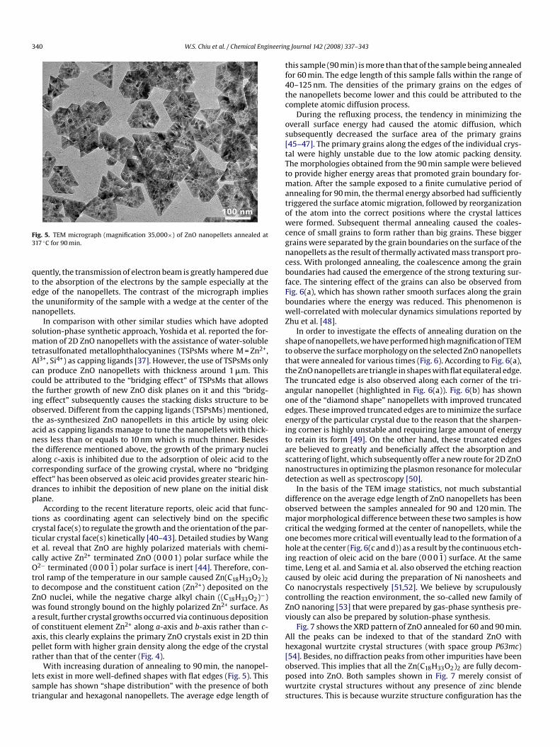
31shapes. The surfaces of the nanopellets are rough and stacked withmany primary grains, which could be attributed to incompleteatomic diffusion. The densities of small primary grains for someof the nanopellets are high along their edges if compared to thatof their center as can be seen in TEM micrograph (Fig. 4). Subse-
Fig. 2. Schematic flow chart for the synthesis of 2D ZnO nanopellets.
as clearly indicating the formation of Zn(C18H33O2)2. Next,hysical separation was done using separation funnel and then(C18H33O2)2 were repeatedly washed with excess warm triple-istilled water to remove the unreacted metal salts. After washingrocess, hexane was evaporated off with a rotavapor, resulting
n organometallic compound of Zn(C18H33O2)2 in the powderorm.
.2. Synthesis of 2D ZnO nanopellets
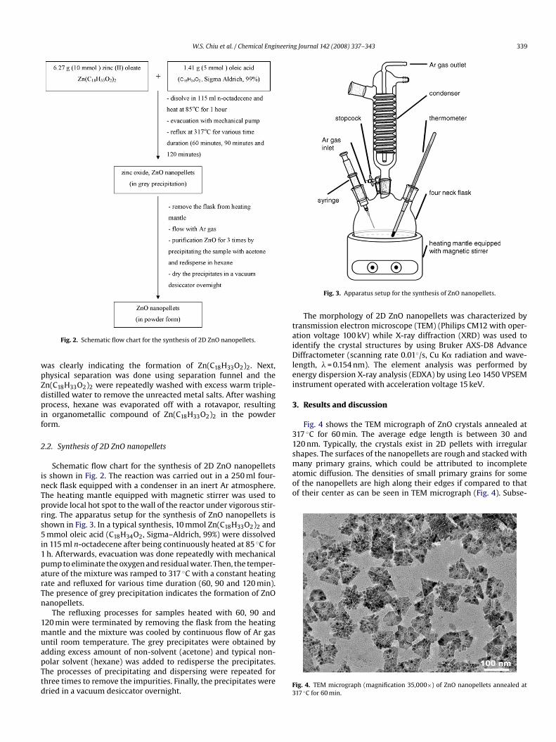
Schematic flow chart for the synthesis of 2D ZnO nanopelletss shown in Fig. 2. The reaction was carried out in a 250 ml four-eck flask equipped with a condenser in an inert Ar atmosphere.he heating mantle equipped with magnetic stirrer was used torovide local hot spot to the wall of the reactor under vigorous stir-ing. The apparatus setup for the synthesis of ZnO nanopellets ishown in Fig. 3. In a typical synthesis, 10 mmol Zn(C18H33O2)2 andmmol oleic acid (C18H34O2, Sigma–Aldrich, 99%) were dissolved
n 115 ml n-octadecene after being continuously heated at 85 ◦C forh. Afterwards, evacuation was done repeatedly with mechanicalump to eliminate the oxygen and residual water. Then, the temper-ture of the mixture was ramped to 317 ◦C with a constant heatingate and refluxed for various time duration (60, 90 and 120 min).he presence of grey precipitation indicates the formation of ZnOanopellets.
The refluxing processes for samples heated with 60, 90 and20 min were terminated by removing the flask from the heatingantle and the mixture was cooled by continuous flow of Ar gas
ntil room temperature. The grey precipitates were obtained by
dding excess amount of non-solvent (acetone) and typical non-olar solvent (hexane) was added to redisperse the precipitates.he processes of precipitating and dispersing were repeated forhree times to remove the impurities. Finally, the precipitates wereried in a vacuum desiccator overnight.F3
Fig. 3. Apparatus setup for the synthesis of ZnO nanopellets.
The morphology of 2D ZnO nanopellets was characterized byransmission electron microscope (TEM) (Philips CM12 with oper-tion voltage 100 kV) while X-ray diffraction (XRD) was used todentify the crystal structures by using Bruker AXS-D8 Advanceiffractometer (scanning rate 0.01◦/s, Cu K� radiation and wave-
ength, � = 0.154 nm). The element analysis was performed bynergy dispersion X-ray analysis (EDXA) by using Leo 1450 VPSEMnstrument operated with acceleration voltage 15 keV.
. Results and discussion
Fig. 4 shows the TEM micrograph of ZnO crystals annealed at17 ◦C for 60 min. The average edge length is between 30 and20 nm. Typically, the crystals exist in 2D pellets with irregular
ig. 4. TEM micrograph (magnification 35,000×) of ZnO nanopellets annealed at17 ◦C for 60 min.
340 W.S. Chiu et al. / Chemical Engineerin
F3
qtetn
smtAcctiotantacedp
tctecOttZwaoapr
lst
tf4tc
os[tTtmatowcgncbfFbwZ
stttTaoeeitasnd
domcohitcCcZv
Ah[54]. Besides, no diffraction peaks from other impurities have been
ig. 5. TEM micrograph (magnification 35,000×) of ZnO nanopellets annealed at17 ◦C for 90 min.
uently, the transmission of electron beam is greatly hampered dueo the absorption of the electrons by the sample especially at thedge of the nanopellets. The contrast of the micrograph implieshe ununiformity of the sample with a wedge at the center of theanopellets.
In comparison with other similar studies which have adoptedolution-phase synthetic approach, Yoshida et al. reported the for-ation of 2D ZnO nanopellets with the assistance of water-soluble
etrasulfonated metallophthalocyanines (TSPsMs where M = Zn2+,l3+, Si4+) as capping ligands [37]. However, the use of TSPsMs onlyan produce ZnO nanopellets with thickness around 1 �m. Thisould be attributed to the “bridging effect” of TSPsMs that allowshe further growth of new ZnO disk planes on it and this “bridg-ng effect” subsequently causes the stacking disks structure to bebserved. Different from the capping ligands (TSPsMs) mentioned,he as-synthesized ZnO nanopellets in this article by using oleiccid as capping ligands manage to tune the nanopellets with thick-ess less than or equals to 10 nm which is much thinner. Besideshe difference mentioned above, the growth of the primary nucleilong c-axis is inhibited due to the adsorption of oleic acid to theorresponding surface of the growing crystal, where no “bridgingffect” has been observed as oleic acid provides greater stearic hin-rances to inhibit the deposition of new plane on the initial disklane.
According to the recent literature reports, oleic acid that func-ions as coordinating agent can selectively bind on the specificrystal face(s) to regulate the growth and the orientation of the par-icular crystal face(s) kinetically [40–43]. Detailed studies by Wangt al. reveal that ZnO are highly polarized materials with chemi-ally active Zn2+ terminated ZnO (0 0 0 1) polar surface while the2− terminated (0 0 0 1) polar surface is inert [44]. Therefore, con-
rol ramp of the temperature in our sample caused Zn(C18H33O2)2o decompose and the constituent cation (Zn2+) deposited on thenO nuclei, while the negative charge alkyl chain ((C18H33O2)−)as found strongly bound on the highly polarized Zn2+ surface. Asresult, further crystal growths occurred via continuous depositionf constituent element Zn2+ along a-axis and b-axis rather than c-xis, this clearly explains the primary ZnO crystals exist in 2D thinellet form with higher grain density along the edge of the crystalather than that of the center (Fig. 4).
With increasing duration of annealing to 90 min, the nanopel-ets exist in more well-defined shapes with flat edges (Fig. 5). Thisample has shown “shape distribution” with the presence of bothriangular and hexagonal nanopellets. The average edge length of
opws
g Journal 142 (2008) 337–343
his sample (90 min) is more than that of the sample being annealedor 60 min. The edge length of this sample falls within the range of0–125 nm. The densities of the primary grains on the edges ofhe nanopellets become lower and this could be attributed to theomplete atomic diffusion process.
During the refluxing process, the tendency in minimizing theverall surface energy had caused the atomic diffusion, whichubsequently decreased the surface area of the primary grains45–47]. The primary grains along the edges of the individual crys-al were highly unstable due to the low atomic packing density.he morphologies obtained from the 90 min sample were believedo provide higher energy areas that promoted grain boundary for-
ation. After the sample exposed to a finite cumulative period ofnnealing for 90 min, the thermal energy absorbed had sufficientlyriggered the surface atomic migration, followed by reorganizationf the atom into the correct positions where the crystal latticesere formed. Subsequent thermal annealing caused the coales-
ence of small grains to form rather than big grains. These biggerrains were separated by the grain boundaries on the surface of theanopellets as the result of thermally activated mass transport pro-ess. With prolonged annealing, the coalescence among the grainoundaries had caused the emergence of the strong texturing sur-ace. The sintering effect of the grains can also be observed fromig. 6(a), which has shown rather smooth surfaces along the grainoundaries where the energy was reduced. This phenomenon isell-correlated with molecular dynamics simulations reported by
hu et al. [48].In order to investigate the effects of annealing duration on the
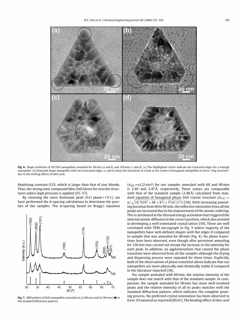
hape of nanopellets, we have performed high magnification of TEMo observe the surface morphology on the selected ZnO nanopelletshat were annealed for various times (Fig. 6). According to Fig. 6(a),he ZnO nanopellets are triangle in shapes with flat equilateral edge.he truncated edge is also observed along each corner of the tri-ngular nanopellet (highlighted in Fig. 6(a)). Fig. 6(b) has shownne of the “diamond shape” nanopellets with improved truncateddges. These improved truncated edges are to minimize the surfacenergy of the particular crystal due to the reason that the sharpen-ng corner is highly unstable and requiring large amount of energyo retain its form [49]. On the other hand, these truncated edgesre believed to greatly and beneficially affect the absorption andcattering of light, which subsequently offer a new route for 2D ZnOanostructures in optimizing the plasmon resonance for molecularetection as well as spectroscopy [50].
In the basis of the TEM image statistics, not much substantialifference on the average edge length of ZnO nanopellets has beenbserved between the samples annealed for 90 and 120 min. Theajor morphological difference between these two samples is how
ritical the wedging formed at the center of nanopellets, while thene becomes more critical will eventually lead to the formation of aole at the center (Fig. 6(c and d)) as a result by the continuous etch-
ng reaction of oleic acid on the bare (0 0 0 1) surface. At the sameime, Leng et al. and Samia et al. also observed the etching reactionaused by oleic acid during the preparation of Ni nanosheets ando nanocrystals respectively [51,52]. We believe by scrupulouslyontrolling the reaction environment, the so-called new family ofnO nanoring [53] that were prepared by gas-phase synthesis pre-iously can also be prepared by solution-phase synthesis.
Fig. 7 shows the XRD pattern of ZnO annealed for 60 and 90 min.ll the peaks can be indexed to that of the standard ZnO withexagonal wurtzite crystal structures (with space group P63mc)
bserved. This implies that all the Zn(C18H33O2)2 are fully decom-osed into ZnO. Both samples shown in Fig. 7 merely consist ofurtzite crystal structures without any presence of zinc blende
tructures. This is because wurzite structure configuration has the
W.S. Chiu et al. / Chemical Engineering Journal 142 (2008) 337–343 341
F 20 min thed
MTt
ht
Ft
(i
ig. 6. Shape evolution of 2D ZnO nanopellets annealed for 90 min (a and b) and 1anopellet. (b) Diamond shape nanopellet with two truncated edges. (c and d) showue to the etching effects of oleic acid.
adelung constant 0.2%, which is larger than that of zinc blende.hus, the strong ionic compound likes ZnO favors for wurzite struc-
ures unless high pressure is applied [55–57].By choosing the most dominant peak (h k l plane = 1 0 1), weave performed the d-spacing calculations to determine the puri-ies of the samples. The d-spacing based on Bragg’s equation
ig. 7. XRD pattern of ZnO nanopellets annealed at (a) 60 min and (b) 90 min ((�) ishe standard diffraction pattern).
wdaipTiicnttfetabnt
sppsif
n (c and d). (a) The highlighted circles indicate the truncated edges for a triangleformation of a hole at the center of hexagonal nanopellets to form “ring structure”
d101 = n�/2 sin �) for our samples annealed with 60 and 90 mins 2.49 and 2.47 A, respectively. These values are comparable
ith that of the standard sample (2.48 A) calculated from stan-ard equation of hexagonal phase ZnO crystal structure (d1 0 1 =/√
(4/3)(h2 + hk + k2) + l2(a2/c2)) [58]. With increasing anneal-ng duration from 60 to 90 min, the reflective intensities from all theeaks are increased due to the improvement of the atomic ordering.his is attributed to the thermal energy activation that triggered thenternal atomic diffusion to the correct position, which also assistedn developing a well-orientated crystal lattice [59]. These are wellorrelated with TEM micrograph in Fig. 5 where majority of theanopellets have well-defined shapes with flat edges if comparedo sample that was annealed for 60 min (Fig. 4). No phase transi-ions have been observed, even though after persistent annealingor 120 min was carried out except the increase in the intensity forach peak. In addition, no agglomerations that caused the phaseransition were observed from all the samples although the dryingnd dispersing process were repeated for three times. Explicitly,oth of the observations of phase transition above indicate that ouranopellets are more physically and chemically stable if comparedo the literature reported [38].
For sample annealed with 60 min, the relative intensity of theample does not match with that of the standard sample. In com-
arison, the sample annealed for 90 min has more well-resolvedeaks and the relative intensity of all its peaks matches with thetandard diffraction pattern, which indicates the complete grow-ng process. No preferred crystal orientation has been observed toorm 1D nanorod as reported [60,61]. The binding effect of oleic acid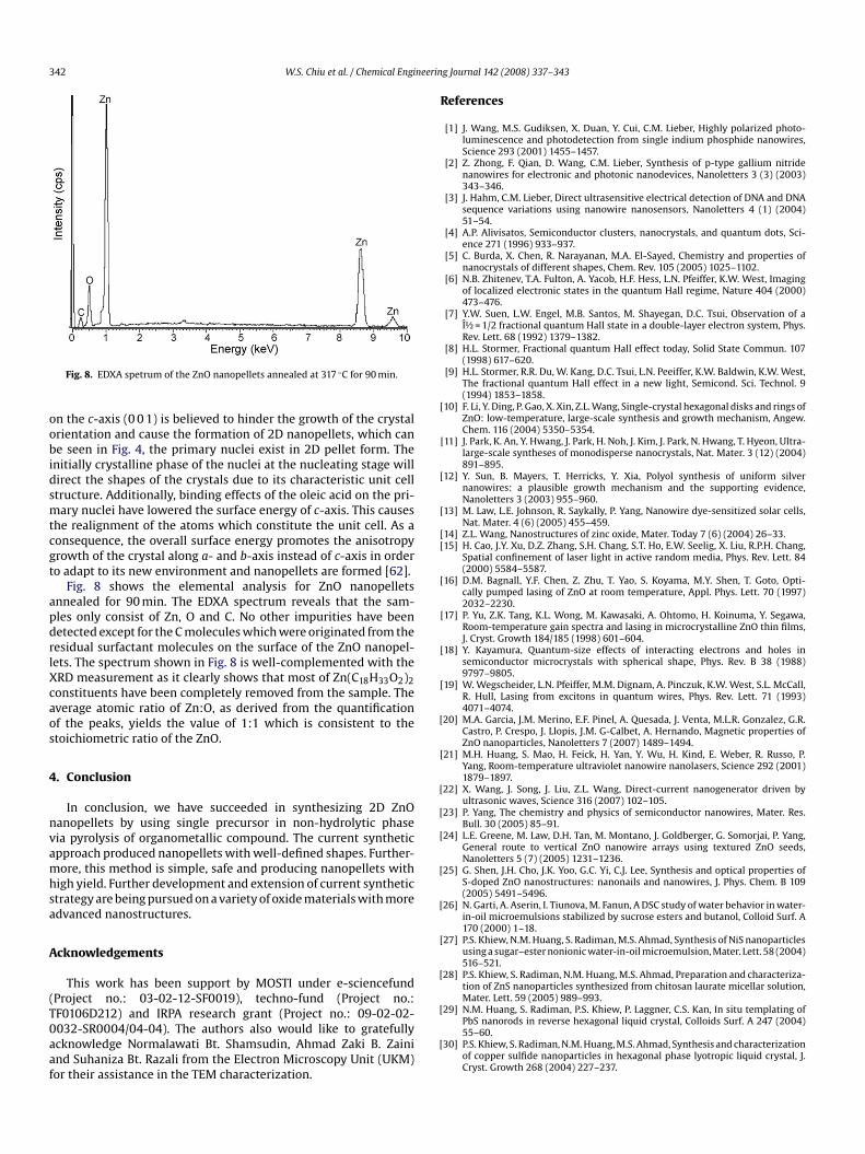
342 W.S. Chiu et al. / Chemical Engineerin
oobidsmtcgt
apdrlXcaos
4
nvamhsa
A
(T0aaf
R
[
[
[
[
[[
[
[
[
[
[
[
[
[
[
[
[
[
[
[29] N.M. Huang, S. Radiman, P.S. Khiew, P. Laggner, C.S. Kan, In situ templating of
Fig. 8. EDXA spetrum of the ZnO nanopellets annealed at 317 ◦C for 90 min.
n the c-axis (0 0 1) is believed to hinder the growth of the crystalrientation and cause the formation of 2D nanopellets, which cane seen in Fig. 4, the primary nuclei exist in 2D pellet form. The
nitially crystalline phase of the nuclei at the nucleating stage willirect the shapes of the crystals due to its characteristic unit celltructure. Additionally, binding effects of the oleic acid on the pri-ary nuclei have lowered the surface energy of c-axis. This causes
he realignment of the atoms which constitute the unit cell. As aonsequence, the overall surface energy promotes the anisotropyrowth of the crystal along a- and b-axis instead of c-axis in ordero adapt to its new environment and nanopellets are formed [62].
Fig. 8 shows the elemental analysis for ZnO nanopelletsnnealed for 90 min. The EDXA spectrum reveals that the sam-les only consist of Zn, O and C. No other impurities have beenetected except for the C molecules which were originated from theesidual surfactant molecules on the surface of the ZnO nanopel-ets. The spectrum shown in Fig. 8 is well-complemented with theRD measurement as it clearly shows that most of Zn(C18H33O2)2onstituents have been completely removed from the sample. Theverage atomic ratio of Zn:O, as derived from the quantificationf the peaks, yields the value of 1:1 which is consistent to thetoichiometric ratio of the ZnO.
. Conclusion
In conclusion, we have succeeded in synthesizing 2D ZnOanopellets by using single precursor in non-hydrolytic phaseia pyrolysis of organometallic compound. The current syntheticpproach produced nanopellets with well-defined shapes. Further-ore, this method is simple, safe and producing nanopellets with
igh yield. Further development and extension of current synthetictrategy are being pursued on a variety of oxide materials with moredvanced nanostructures.
cknowledgements
This work has been support by MOSTI under e-sciencefundProject no.: 03-02-12-SF0019), techno-fund (Project no.:F0106D212) and IRPA research grant (Project no.: 09-02-02-
032-SR0004/04-04). The authors also would like to gratefullycknowledge Normalawati Bt. Shamsudin, Ahmad Zaki B. Zainind Suhaniza Bt. Razali from the Electron Microscopy Unit (UKM)or their assistance in the TEM characterization.[
g Journal 142 (2008) 337–343
eferences
[1] J. Wang, M.S. Gudiksen, X. Duan, Y. Cui, C.M. Lieber, Highly polarized photo-luminescence and photodetection from single indium phosphide nanowires,Science 293 (2001) 1455–1457.
[2] Z. Zhong, F. Qian, D. Wang, C.M. Lieber, Synthesis of p-type gallium nitridenanowires for electronic and photonic nanodevices, Nanoletters 3 (3) (2003)343–346.
[3] J. Hahm, C.M. Lieber, Direct ultrasensitive electrical detection of DNA and DNAsequence variations using nanowire nanosensors, Nanoletters 4 (1) (2004)51–54.
[4] A.P. Alivisatos, Semiconductor clusters, nanocrystals, and quantum dots, Sci-ence 271 (1996) 933–937.
[5] C. Burda, X. Chen, R. Narayanan, M.A. El-Sayed, Chemistry and properties ofnanocrystals of different shapes, Chem. Rev. 105 (2005) 1025–1102.
[6] N.B. Zhitenev, T.A. Fulton, A. Yacob, H.F. Hess, L.N. Pfeiffer, K.W. West, Imagingof localized electronic states in the quantum Hall regime, Nature 404 (2000)473–476.
[7] Y.W. Suen, L.W. Engel, M.B. Santos, M. Shayegan, D.C. Tsui, Observation of aI½ = 1/2 fractional quantum Hall state in a double-layer electron system, Phys.Rev. Lett. 68 (1992) 1379–1382.
[8] H.L. Stormer, Fractional quantum Hall effect today, Solid State Commun. 107(1998) 617–620.
[9] H.L. Stormer, R.R. Du, W. Kang, D.C. Tsui, L.N. Peeiffer, K.W. Baldwin, K.W. West,The fractional quantum Hall effect in a new light, Semicond. Sci. Technol. 9(1994) 1853–1858.
10] F. Li, Y. Ding, P. Gao, X. Xin, Z.L. Wang, Single-crystal hexagonal disks and rings ofZnO: low-temperature, large-scale synthesis and growth mechanism, Angew.Chem. 116 (2004) 5350–5354.
11] J. Park, K. An, Y. Hwang, J. Park, H. Noh, J. Kim, J. Park, N. Hwang, T. Hyeon, Ultra-large-scale syntheses of monodisperse nanocrystals, Nat. Mater. 3 (12) (2004)891–895.
12] Y. Sun, B. Mayers, T. Herricks, Y. Xia, Polyol synthesis of uniform silvernanowires: a plausible growth mechanism and the supporting evidence,Nanoletters 3 (2003) 955–960.
13] M. Law, L.E. Johnson, R. Saykally, P. Yang, Nanowire dye-sensitized solar cells,Nat. Mater. 4 (6) (2005) 455–459.
14] Z.L. Wang, Nanostructures of zinc oxide, Mater. Today 7 (6) (2004) 26–33.15] H. Cao, J.Y. Xu, D.Z. Zhang, S.H. Chang, S.T. Ho, E.W. Seelig, X. Liu, R.P.H. Chang,
Spatial confinement of laser light in active random media, Phys. Rev. Lett. 84(2000) 5584–5587.
16] D.M. Bagnall, Y.F. Chen, Z. Zhu, T. Yao, S. Koyama, M.Y. Shen, T. Goto, Opti-cally pumped lasing of ZnO at room temperature, Appl. Phys. Lett. 70 (1997)2032–2230.
17] P. Yu, Z.K. Tang, K.L. Wong, M. Kawasaki, A. Ohtomo, H. Koinuma, Y. Segawa,Room-temperature gain spectra and lasing in microcrystalline ZnO thin films,J. Cryst. Growth 184/185 (1998) 601–604.
18] Y. Kayamura, Quantum-size effects of interacting electrons and holes insemiconductor microcrystals with spherical shape, Phys. Rev. B 38 (1988)9797–9805.
19] W. Wegscheider, L.N. Pfeiffer, M.M. Dignam, A. Pinczuk, K.W. West, S.L. McCall,R. Hull, Lasing from excitons in quantum wires, Phys. Rev. Lett. 71 (1993)4071–4074.
20] M.A. Garcia, J.M. Merino, E.F. Pinel, A. Quesada, J. Venta, M.L.R. Gonzalez, G.R.Castro, P. Crespo, J. Llopis, J.M. G-Calbet, A. Hernando, Magnetic properties ofZnO nanoparticles, Nanoletters 7 (2007) 1489–1494.
21] M.H. Huang, S. Mao, H. Feick, H. Yan, Y. Wu, H. Kind, E. Weber, R. Russo, P.Yang, Room-temperature ultraviolet nanowire nanolasers, Science 292 (2001)1879–1897.
22] X. Wang, J. Song, J. Liu, Z.L. Wang, Direct-current nanogenerator driven byultrasonic waves, Science 316 (2007) 102–105.
23] P. Yang, The chemistry and physics of semiconductor nanowires, Mater. Res.Bull. 30 (2005) 85–91.
24] L.E. Greene, M. Law, D.H. Tan, M. Montano, J. Goldberger, G. Somorjai, P. Yang,General route to vertical ZnO nanowire arrays using textured ZnO seeds,Nanoletters 5 (7) (2005) 1231–1236.
25] G. Shen, J.H. Cho, J.K. Yoo, G.C. Yi, C.J. Lee, Synthesis and optical properties ofS-doped ZnO nanostructures: nanonails and nanowires, J. Phys. Chem. B 109(2005) 5491–5496.
26] N. Garti, A. Aserin, I. Tiunova, M. Fanun, A DSC study of water behavior in water-in-oil microemulsions stabilized by sucrose esters and butanol, Colloid Surf. A170 (2000) 1–18.
27] P.S. Khiew, N.M. Huang, S. Radiman, M.S. Ahmad, Synthesis of NiS nanoparticlesusing a sugar–ester nonionic water-in-oil microemulsion, Mater. Lett. 58 (2004)516–521.
28] P.S. Khiew, S. Radiman, N.M. Huang, M.S. Ahmad, Preparation and characteriza-tion of ZnS nanoparticles synthesized from chitosan laurate micellar solution,Mater. Lett. 59 (2005) 989–993.
PbS nanorods in reverse hexagonal liquid crystal, Colloids Surf. A 247 (2004)55–60.
30] P.S. Khiew, S. Radiman, N.M. Huang, M.S. Ahmad, Synthesis and characterizationof copper sulfide nanoparticles in hexagonal phase lyotropic liquid crystal, J.Cryst. Growth 268 (2004) 227–237.
neerin
[
[
[
[
[
[
[
[
[
[
[
[
[
[
[
[
[
[
[
[
[
[
[
[
[
[
[
[
[
[
W.S. Chiu et al. / Chemical Engi
31] P.S. Khiew, S. Radiman, N.M. Huang, M.S. Ahmad, Studies on the growth andcharacterization of CdS and PbS nanoparticles using sugar–ester nonionicwater-in-oil microemulsion, J. Cryst. Growth 254 (2003) 235–243.
32] P.S. Khiew, S. Radiman, N.M. Huang, M.S. Ahmad, In situ polymerization ofconducting polyaniline in bicontinuous cubic phase of lyotropic liquid crystal,Colloids Surf. A-Physicochem. Eng. Asp. 247 (2004) 35–40.
33] N.M. Huang, C.S. Kan, P.S. Khiew, S. Radiman, Single w/o microemulsion tem-plating of CdS nanoparticles, J. Mater. Sci. 39 (2004) 2411–2415.
34] P.S. Khiew, N.M. Huang, S. Radiman, M.S. Ahmad, Synthesis of NiS nanoparticlesusing a sugar–ester nonionic water-in-oil microemulsion, Mater. Lett. 58 (2004)762–767.
35] S. Hirano, K. Masuya, M. Kuwabara, Multi-nucleation-based formation of ori-ented zinc oxide microcrystals and films in aqueous solutions, J. Phys. Chem. B108 (2004) 4576–4578.
36] C.L. Kuo, T.J. Kuo, M.H. Huang, Hydrothermal synthesis of ZnO microspheresand hexagonal microrods with sheetlike and platelike nanostructures, J. Phys.Chem. B 109 (43) (2005) 20115–20121.
37] T. Yoshida, M. Tochimoto, D. Schlettwein, D. Wohrle, T. Sugiura, H. Minoura,Self-assembly of zinc oxide thin films modified with tetrasulfonated met-allophthalocyanines by one-step electrodeposition, Chem. Mater. 11 (1999)2657–2667.
38] N. Pinna, K. Weiss, H.S. Kongehl, W. Vogel, J. Urban, M.P. Pileni, TriangularCdS nanocrystals: synthesis, characterization, and stability, Langmuir 17 (2001)7982–7987.
39] P. Fons, H. Tampo, A.V. Kolobov, M. Ohkubo, S. Niki, J. Tominaga, R. Carboni,F. Boscherini, S. Friedrich, Direct observation of nitrogen location in molec-ular beam epitaxy grown nitrogen-doped ZnO, Phys. Rev. Lett. 96 (2006)045504–045505.
40] W.S. Chiu, S. Radiman, M.H. Abdullah, P.S. Khiew, N.M. Huang, R. Abd-Shukor,One pot synthesis of monodisperse Fe3O4 nanocrystals by pyrolysis reaction oforganometallic compound, Mater. Chem. Phys. 106 (2007) 231–235.
41] X. Peng, Mechanisms for the shape-control and shape-evolution of colloidalsemiconductor nanocrystals, Adv. Mater. 15 (5) (2003) 459–463.
42] W.W. Yu, Y.A. Wang, X. Peng, Formation and stability of size-, shape-, andstructure-controlled CdTe nanocrystals: ligand effects on monomers andnanocrystals, Chem. Mater. 15 (2003) 4300–4308.
43] W.W. Yu, X. Peng, Formation of high-quality CdS and other II–VI semiconduc-tor nanocrystals in noncoordinating solvents: tunable reactivity of monomers,Angew. Chem. Int. Ed. 41 (13) (2002) 2368–2371.
44] Z.L. Wang, X.Y. Kong, J.M. Zuo, Induced growth of asymmetric nanocantilever
arrays on polar surfaces, Phys. Rev. Lett. 91 (18) (2003) 185502–185505.45] W.S. Chiu, S. Radiman, R. Abd-Shukor, M.H. Abdullah, P.S. Khiew, Tunable coer-civity of CoFe2O4 nanoparticles via thermal annealing treatment, J. Alloy Comp.459 (2008) 291–297.
46] J.O. Bovin, R.L. Wallember, D. Smith, Imaging of atomic clouds outside the sur-faces of gold crystals by electron microscopy, Nature 317 (1985) 47–49.
[
[
g Journal 142 (2008) 337–343 343
47] S. Iijima, H. Ichihashi, Structural instability of ultrafine particles of metals, Phys.Rev. Lett. 56 (1986) 616–619.
48] H. Zhu, R.S. Averback, Sintering processes of two nanoparticles: astudy by molecular dynamics simulations, Philos. Magn. Lett. 73 (1996)27–33.
49] B.J. Wiley, S.H. Im, Z.Y. Li, J. McLellan, A. Siekkinen, Y. Xia, Maneuvering thesurface plasmon resonance of silver nanostructures through shape-controlledsynthesis, J. Phys. Chem. B 110 (2006) 15666–15675.
50] K.L. Kelly, E. Corondo, L.L. Zhao, G.C. Sxhatz, The optical properties of metalnanoparticles: the influence of size, shape, and dielectric environment, J. Phys.Chem. B 107 (2003) 668–677.
51] Y. Leng, Y. Zhang, T. Liu, M. Suzuki, X. Li, Synthesis of single crystalline triangularand hexagonal Ni nanosheets with enhanced magnetic properties, Nanotech-nology 17 (6) (2006) 1797–1800.
52] A.C.S. Samia, K. Hyzer, J.A. Schlueter, C. Qin, J.S. Jiang, X.D. Bader, X. Lee, Ligandeffect on the growth and the digestion of Co nanocrystals, J. Am. Chem. Soc. 127(2005) 4126–4127.
53] X.Y. Kong, Z.L. Wang, Spontaneous polarization-induced nanohelixes,nanosprings and nanorings of piezoelectric nanobelts, Nanoletters 3 (12)(2003) 1625–1631.
54] Joint Committee for Powder Diffraction Society (JCPDS), Powder DiffractionDatabase, pattern: 36-1451.
55] C.Y. Yeh, Z.W. Lu, S. Froyen, A. Zunger, Zinc-blende? wurtzite polytypism insemiconductors, Phys. Rev. B 46 (1992) 10086–10097.
56] C.Y. Yeh, S.H. Wei, A. Zunger, Relationships between the band gaps of the zinc-blende and wurtzite modifications of semiconductors, Phys. Rev. B 50 (1994)2715–2718.
57] J. Serrano, A.H. Romero, F.J. Manjon, R. Lauck, M. Cardona, A. Rubio, Pressuredependence of the lattice dynamics of ZnO: an ab initio approach, Phys. Rev. B69 (2004) 094306–094319.
58] J.F. Shackelford, Introduction to Material Science for Engineers, 6th ed., Pearson-Prentice Hall, USA, 2004, p. 106.
59] E.V. Shevchenko, D.V. Talapin, H. Schnablegger, A. Kornowski, O. Festin, P.Svedlindh, M. Haase, H. Weller, Study of nucleation and growth in theorganometallic synthesis of magnetic alloy nanocrystals: the role of nucle-ation rate in size control of CoPt3 nanocrystals, J. Am. Chem. Soc. 125 (2003)9090–9101.
60] Q. Li, V. Kumar, Y. Li, H. Zhang, T.J. Marks, R.P.H. Chang, Fabrication ofZnO nanorods and nanotubes in aqueous solutions, Chem. Mater. 17 (2005)1001–1006.
61] L. Xu, Y. Guo, Q. Liao, J. Zhang, D. Xu, Morphological control of ZnOnanostructures by electrodeposition, J. Phys. Chem. B 109 (28) (2005)13519–13522.
62] Y. Jun, J. Lee, J. Choi, J. Cheon, Symmetry-controlled colloidal nanocrystals:nonhydrolytic chemical synthesis and shape determining parameters, J. Phys.Chem. B 109 (2005) 14795–14806.