Embed Size (px)
Citation preview

Chemical and Electronic Properties of DNA-immobilized InAs
for Biosensor applications
By
EunKyung Cho
A dissertation submitted in partial fulfillment of
the requirements for the degree of
Doctor of Philosophy
(Chemical and Biological Engineering)
at the
UNIVERSITY of WISCONSIN-MADISON
2012
Date of final oral examination: 12/12/12
The dissertation is approved by the following members of the Final Oral Committee:
Thomas F. Kuech, Professor, Chemical and Biological Engineering
James A. Dumesic, Professor, Chemical and Biological Engineering
Manos Mavrikakis, Professor, Chemical and Biological Engineering
George W. Huber, Professor, Chemical and Biological Engineering
April S. Brown, Professor, Electrical and Computer Engineering (Duke University)

i
Chemical and Electronic properties of DNA-
immobilized InAs for Biosensor applications
EunKyung Cho
Under the supervision of Professor Thomas F. Kuech
At the University of Wisconsin – Madison
Single-stranded DNA immobilized on an III−V semiconductor has potential as
high-sensitivity biosensor. The chemical and electronic changes occurring upon the
binding of DNA to the InAs surface are essential to understanding the DNA-
immobilization mechanism. In this work, the chemical and electronic properties of DNA-
immobilized InAs surfaces were determined through high-resolution X-ray photoelectron
spectroscopy (XPS), near-edge X-ray absorption fine structure (NEXAFS), and
ultraviolet photoelectron spectroscopy (UPS). Prior to DNA functionalization, sulfur
passivation and HF- and NH4OH- based aqueous etches were used to alter the surface
chemistry of the InAs surface. The initial chemical states of the surface resulting from
these chemical treatments were characterized prior to functionalization. F-tagged
thiolated single-strand DNA (ssDNA) was used as the probe species under two different
functionalization methods. The presence of DNA immobilized on the surface was
confirmed from the F 1s, N 1s, and P 2p peaks in the XPS spectra. The presence of NaCl
in the functionalization solution substantially increased the density of immobilized DNA
on the InAs surface. The interfacial chemistry was studied using an analysis of the As 3d

ii
and In 3d spectra indicating that both In−S and As−S are present on the surface after
DNA functionalization. The amount of In−S and As−S was determined by the
functionalization method as well as the presence of NaCl during functionalization. The
orientation of the adsorbed ssDNA is determined by polarization-dependent NEXAFS
utilizing the N K-edge. The immobilized ssDNA molecule has a preferred tilt angle with
respect to the substrate normal, but with a random azimuthal distribution. The electronic
properties of DNA-immobilized InAs surfaces such as band bending and work function
were also studied using XPS and UPS. The DNA functionalization method determines
not only the interface chemistry, but also a surface state density and surface band bending.
The surface potential influenced by the density of the immobilized-DNA. The influence
of the DNA attachment on the chemical and electronic structure of InAs surfaces
provides insight into how the chemical and electronic properties of the InAs surfaces
modulated with the DNA immobilization showing the potential use of InAs substrate for
biosensor applications.
Approved ____________________
____________________

iii
Acknowledgements
I have been fortunate to work with many people who provide me the generous
assistance during my time at UW-Madison. I know this work would have never been
accomplished without their support. I am indebted to them for their time and labor.
First of all, I would like to thank my advisor, Professor Thomas Kuech, for his
support and guidance in my research throughout my graduate school career. He had given
me a freedom to choose research project and decide what I would like to explore. He had
shown me insight and patience when I encountered frustrating barrier in research. I am
also grateful his understanding in my personal life events.
I would like to thank Professor April Brown (Duke University) for valuable
discussions regarding the biosensor project. I thank her research group for their
collaboration and assistance in XPS and AFM experiments. I also want to thank Dr.
Nathan Guisinger (Argonne National Laboratory) for his countless efforts on STM work.
He taught me how to synthesize graphene and constantly contributed ideas to our work.
Thanks to his postdoc, Dr. Esmeralda Yitamben, for assistance in the STM experiments.
Also, I would like to thank the members of Kuech group, both past and present,
for their kind help. I would especially like to acknowledge the past students, John Uhlrich
and Smita Jha. John introduced me our UHV system and showed me how to use the
XPS/UPS system. Smita helped me to settle down in our lab and encouraged me when I
had been overwhelmed by a new life in Madison. I also thank Monika, David, Kevin, and
Brian for helping me with proofreading my writing.

iv
I also had a great deal of help from Mary Severson and Mark Bissen (Synchrotron
radiation center). They had assisted in NEXAFS runs. I would like to thank Phillip
Johnson for useful discussions regarding NEXAFS analysis.
I would like to have a personal acknowledgement. I thank my good friends who
I’ve met at KCCM (too many to list here but you know who you are!) for providing
support and help that I needed.
I wish to thank my family for unconditional support and love. I especially thank
my parents. They believe in me more than I believe in myself when I encountered
difficulties in my life.
The best outcome from my time in Madison is finding my husband, SungIk, and
having our son, Alexander Minseung. I married the best person out there for me. He has
been a great supporter and has unconditionally loved me. There is no suitable word that
can fully describe how much I love him. I truly thank him for sticking by my side, even
when I didn’t have faith in myself. I can’t say that it has not been challenging of raising
our son during our Ph.D. career, but our son brings us true happiness. I have never been
so happy as when our son smiles at me. Thanks for being there Alex. We really love you.

v
Table of Contents
Abstract ...............................................................................................................................i
Acknowledgements .......................................................................................................... iii
Table of Contents .............................................................................................................. v
List of Figures ................................................................................................................ viii
List of Tables .................................................................................................................. xii
1. Introduction ................................................................................................................. 1
1.1 Motivation .......................................................................................................... 1
1.2 Focus of this Study ............................................................................................. 3
2. Background ................................................................................................................. 7
2.1 Semiconductor Surfaces ..................................................................................... 7
2.1.1 Surface States and Band Bending .................................................... 7
2.1.2 Chemisorption and Surface Chemistry .......................................... 10
2.1.3 Depletion Region and Space Charge ............................................. 14
2.2 InAs ................................................................................................................ 15
2.2.1 Physical Properties ........................................................................ 15
2.2.2 Band Structure and Electron Accumulation Layer ........................ 15
2.2.3 Surface Cleaning ............................................................................ 18
2.2.4 Surface Passivation ....................................................................... 18
2.3 DNA Biosensor ............................................................................................... 20
2.3.1 DNA Properties .............................................................................. 20
2.3.2 Biosensors ...................................................................................... 24
2.3.3 Semiconductor-based Biosensors .................................................. 26
2.4 Graphene ........................................................................................................ 27
2.4.1 Formation ...................................................................................... 27
2.4.2 Structure and Physical Properties .................................................. 28
2.4.3 Band structure and Electronic Properties ...................................... 30

vi
2.4.4 Graphene-based Materials for Catalysis ........................................ 32
3. Experimental Techniques .......................................................................................... 38
3.1 Photoelectron Spectroscopy ............................................................................. 38
3.1.1 Photoemission phenomena............................................................. 38
3.1.2 X-ray Photoelectron Spectroscopy ................................................ 40
3.1.3 Ultraviolet Photoelectron Spectroscopy ........................................ 45
3.2 Near edge X-ray Absorption Fine Structure .................................................... 49
3.3 Atomic Force Microscopy ............................................................................... 53
3.3.1 Kelvin Probe Force Microscopy ................................................... 55
3.4 Scanning Tunneling Microscopy ..................................................................... 57
3.4.1 Scanning Tunneling Spectroscopy ................................................. 59
4. DNA immobilization on sulfur-passivated InAs surfaces ..................................... 63
4.1 Introduction ..................................................................................................... 63
4.2 Experimental .................................................................................................. 65
4.3 Results and Discussion .................................................................................... 66
4.3.1 Sulfur passivation........................................................................... 66
4.3.2 Effect of sulfur passivation on DNA functionalization ................. 71
4.4 Conclusions .................................................................................................. 75
5. Chemical and Electrical Characterization of DNA-immobilized InAs surfaces
using XPS, UPS and NEXAFS .................................................................................. 78
5.1 Introduction .................................................................................................. 78
5.2 Experimental .................................................................................................. 80
5.2.1 Materials ........................................................................................ 80
5.2.2 Sample Preparation ........................................................................ 81
5.2.3 XPS and UPS characterization ....................................................... 82
5.2.4 NEXAFS characterization ............................................................. 83
5.3 Results and Discussion .................................................................................... 85
5.3.1 XPS analysis of clean InAs surfaces .............................................. 85
5.3.2 Immobilized DNA on InAs surfaces.............................................. 86

vii
5.3.3 Interface Chemistry ........................................................................ 90
5.3.4 NEXAFS Studies ........................................................................... 94
5.3.5 Electronic Properties ...................................................................... 96
5.4 Conclusions ................................................................................................ 103
6. Effect of Salt on DNA immobilization .................................................................... 107
6.1 Introduction ................................................................................................ 107
6.2 Experimental ................................................................................................ 109
6.3 Results and Discussion .................................................................................. 111
6.3.1 Effect of Salt on DNA immobilization efficiency ....................... 111
6.3.2 Interface Chemistry ...................................................................... 114
6.3.3 NEXAFS Orientation Studies ...................................................... 121
6.3.4 Electronic Properties .................................................................... 125
6.4 Conclusions .................................................................................................... 129
7. Platinum Nanoclusters on Graphene grown on SiC(0001) ................................. 133
7.1 Introduction ................................................................................................ 133
7.2 Experimental ................................................................................................ 135
7.3 Results and Discussion .................................................................................. 135
7.3.1 Deposition of Pt on Graphene ...................................................... 135
7.3.2 Electronic properties of Pt/Graphene surface .............................. 139
7.3.3 Thermal Stability of Pt clusters on Graphene .............................. 143
7.4 Conclusions ................................................................................................ 149
8. Conclusions and Recommendations ....................................................................... 152
8.1 Conclusions ................................................................................................ 152
8.2 Recommendations for Future Work ............................................................... 157

viii
List of Figures:
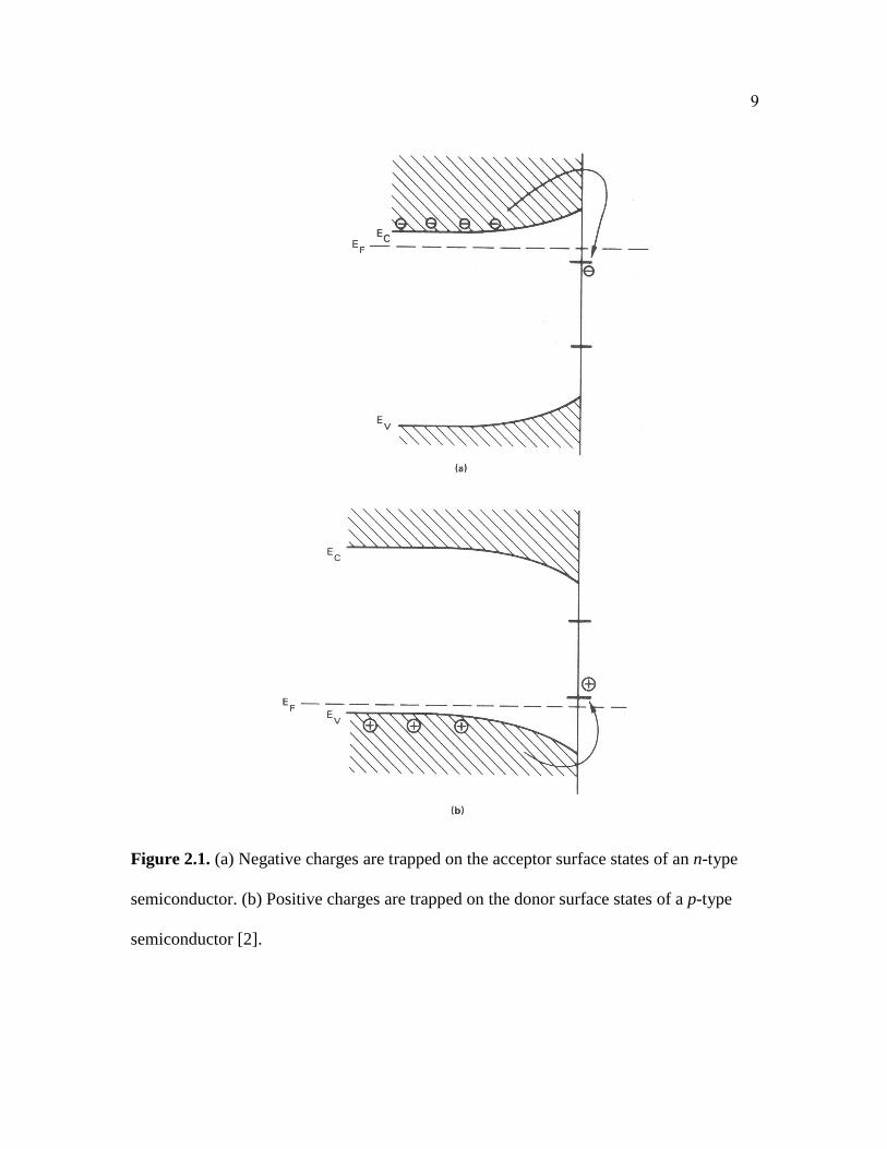
Figure 2.1. (a) Negative charges are trapped on the acceptor surface states of an n-
type semiconductor. (b) Positive charges are trapped on the donor surface states of a p-
type semiconductor.
Figure 2.2. Formation of band bending with acceptor surface states (A1 and A2) with
no charge transfer to surface states (a, b) and at equilibrium (a’ and b’). The acceptor
surface states create a negative charge on the surface resulting in upward band bending.
The upper diagrams show the energy band for an n-type semiconductor surface and the
bottom diagram represents the energy band for a p-type semiconductor surface.
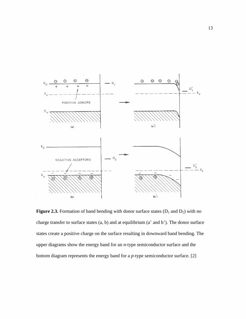
Figure 2.3. Formation of band bending with donor surface states (D1 and D2) with no
charge transfer to surface states (a, b) and at equilibrium (a’ and b’). The donor surface
states create a positive charge on the surface resulting in downward band bending. The
upper diagrams show the energy band for an n-type semiconductor surface and the
bottom diagram represents the energy band for a p-type semiconductor surface.
Figure 2.4. Band structure of InAs.
Figure 2.5. Chemical Structure of Nucleotide.
Figure 2.6. Structure of purine, pyrimidine and nucleobases.
Figure 2.7. Electronic DNA biosensor. The immobilized DNA is a recognition layer
and corresponding DNA is an analyte. The binding event is transferred into a measurable
electronic signal.
Figure 2.8. Graphene structure. Red and green colors indicate the two triangular
sublattices, labeled A and B.
Figure 2.9. (a) Graphene band structure of a carbon monolayer. The conduction band
(E>0) and the valence band (E<0) form conically shaped valleys that touch at the six
corners of the Brillouin zone (called Dirac points, or K points). The three corners marked
by a white dot and black dot are equivalent, respectively. (b) Low-energy dispersion at
one of the K points shows the symmetric Dirac cone structure.
Figure 3.1. Diagram illustrating the photoemission process from a solid material.
Figure 3.2. Energy diagram of the photoemission process under the assumption of a
conductive sample in electrical contact with the spectrometer and hence possesses a
common Fermi level.

ix
Figure 3.3. X-ray emission spectrum in linear (upper curve) and logarithmic (lower
curve) intensity plots, from an aluminum target excited with electrons with a kinetic
energy of 15 kV.
Figure 3.4. A schematic of a typical core level photoemission spectrum.
Figure 3.5. Universal curve for the dependence of the attenuation length on the kinetic
energy of the electron.
Figure 3.6. Example valence band spectra of sputtered gold. The ionization potential
(IP) is found by subtracting the width of the spectra (W) from the incident photon energy
(hν) as shown.
Figure 3.7. a) Band energy diagram depicting NEXAFS resonant excitations. Incident
soft X-ray photons excite 1s electrons to unfilled molecular orbitals such as the π* or σ*.
Excitation to the continuum, as shown here, can occur at energies above the absorption
edge. b) Directional resonances are dependent on the spatial location of the final state
orbital, and can be expressed as vectors or planes.
Figure 3.8. Carbon K-edge NEXAFS spectra and chemical structures of carbohydrate
and amino sugars
Figure 3.9. Schematic of an apparatus for atomic force microscopy.
Figure 3.10. Schematic band diagram of tip and sample.
Figure 3.11. Scanning tunneling microscope (STM). A bias is applied between the
sample and the tip. As the tip is scanned from left to right, either (a) the tip is moved
vertically to keep current constant (constant current imaging), or (b) the vertical position
is held constant and the current varies (constant height imaging).
Figure 4.1. UPS valence band spectra for the clean InAs(100) surface and sulfur-
passivated InAs surface.
Figure 4.2. XPS of As 3d core-level spectra for InAs surfaces. (a) The sample after
sulfur passivation shows As-In (BE = 40.9 eV) peak with negligible amount of As-Ox
(BE = 44-45 eV) and As-S (BE ≈ 42 eV). (b) The sample after functionalization of
passivated surface shows not only As-In but also As-Ox, indicated by the dashed line.
Figure 4.3. Fluorescence measurement of functionalized samples (a) without sulfur
passivation and (b) with sulfur passivation.

x
Figure 5.1. As 3d and In3d5/2 spectrum of as-received and cleaned InAs samples: as-
received InAs sample (C0); NH4OH-etched InAs (C1); HF-etched InAs (C2); HF-etched
and annealed InAs (C3). The annealing step was carried out in UHV at 380oC. A doublet
separation of 0.69 eV for As 3d region and 7.55 eV for In 3d region was used and spin-
orbit splitting intensity ratio was 0.67 for both spectra.
Figure 5.2. High-resolution XPS spectra of the (a) F 1s, (b) N 1s and (c) P 2p core
levels from the functionalized samples (C1A, C2A, C3A, C1B, C2B, and C3B). The N 1s
region was deconvolved into two components associated with the primary amine and
imino groups. Peak binding energies for the spectra were referenced to the adventitious C
1s component at 285.0 eV.
Figure 5.3. High-resolution XPS spectra of the (a) As 3d and (b) In 3d5/2 region for
the functionalized InAs. A doublet separation of 0.69 eV and intensity ratio of 0.67 was
used for As 3d5/2 and As 3d3/2 peak components. Spin-orbit splitting of In 3d peaks was
7.55 eV and intensity ratio was 0.67 for the doublet.
Figure 5.4. Carbon K-edge NEXAFS spectra for the C1A and C1B samples. The C1M
sample was only treated with MCH without DNA probe in the functionalization solution.
The σ*CH peak is positioned at 287.3 eV, the peak at 288.5 eV is attributed to the
σ*CO ,and the σ
*CNH peak is found at 289 eV.
Figure 5.5. The binding energy of As-In component in the As 3d5/2 core-level for
DNA functionalized InAs samples.
Figure 5.6. (a) UPS spectra and (b) secondary electron emission edge of the spectra
for the C1A and C1B. The high energy cutoff was found at 16.25 eV for the C1A and
C1B samples.
Figure 6.1. High-resolution XPS spectra of the (a) N 1s and (b) P 2p region for the
functionalized InAs obtained from C1A and C1B prepared with and without salt.
Figure 6.2. High-resolution XPS spectra of the (a) As 3d, (b) As 2p3/2, and (c) In 3d5/2
region for the clean and functionalized InAs.
Figure 6.3. Carbon K-edge NEXAFS spectra for the C1A – NaCl and C1B – NaCl
samples. The σ*CH peak is positioned at 287.3 eV, the peak at 288.5 eV is attributed to
the σ*CO ,and the σ
*CNH peak is found at 289 eV.
Figure 6.4. Nitrogen K-edge NEXAFS spectra from mixed DNA/MCH on InAs
surface measured at the angle between normal (90°) and glancing (20°) incident X-ray
angles.

xi
Figure 6.5. Polarization dependence of the intensities of the π* resonance in the N K-
edge NEXAFS spectra of C1B – NaCl sample.
Figure 6.6. (a) UPS spectra and (b) secondary electron emission edge of the spectra
for the C1B and C1B-NaCl. The high energy cutoff was found at 16.25 eV for the C1B
sample and 16.10 eV for the C1B-NaCl sample.
Figure 6.7. Surface band diagrams at the surface. The left side of diagram is C1B, and
right side of diagram is C1B-NaCl sample.
Figure 7.1 STM images of (a) clean graphene/SiC(0001), (b) 1 min, (c) 3 min, (d) 5
min, (e) 10 min, and (f) 30 min doses of Pt deposited on graphene/SiC(0001) at sample
bias V= –1.0 V and tunneling current I=100 pA at 300 K ((a)-(f) 100x100 nm2, scale bar
in (a) = 25 nm (a) insert 2.5 nm2).
Figure 7.2 Cluster height distrubution as a function of the corresponding cluster
diameter for 5 min doses of Pt deposited on graphene/SiC(0001).
Figure 7.3 (a) Schematic structure and STM topographic image of a Pt-deposited
graphene/SiC(0001) sample, (b)-(c) STM topographic images of the surface after a 5 min
deposition of Pt at sample bias V= –1.0 V and tunneling current I=200 pA, imaged at 300
K (scale bar = 5 nm in (b), 2 nm in (c), respectively), (d) STS spectrum of clean
monolayer graphene, and (e) STS spectra of various Pt clusters. The corresponding
measurement points are shown in (c).
Figure 7.4 STM images of the graphene/SiC(0001) sample after a 5 min deposition of
Pt and anneal at (a) 400 °C, (b) 500 °C, (c) 600 °C, and (d) 700 °C each for one hour and
imaged at sample bias V= –0.3 V and tunneling current I=100 pA at 55 K. (Scale bar =
10 nm).
Figure 7.5 Size distribution of the graphene/SiC(0001) sample after a 5 min
deposition of Pt (a) as-deposited, (b) after anealing at 400 °C, and (c) after annealing at
700 °C.
Figure 7.6 (a-b) STM topographic images of the graphene/SiC(0001) sample after a 5
min deposition of Pt annealed at 1250 °C and imaged at sample bias V = –1.0 V,
tunneling current I = 100 pA at 300 K. (scale bar = 50 nm in (a), 25 nm in (b)), (c)
schematic structure of the Pt-deposited graphene/SiC(0001) surface after flashing
indicating the intercalation of Pt.

xii
List of Tables:
Table 4.1. Normalized intensities of XPS peaks for the sulfur-passivated InAs.
Table 4.2. Normalized intensities of XPS peaks for the functionalized InAs without and
with sulfur passivation.
Table 5.1. Sample nomenclature
Table 5.2. Binding Energy of main components for As 3d and In 3d5/2 core levels
Table 5.3. XPS compositional Data for functionalized samples.
Table 6.1. XPS High-resolution C 1s chemical species of the functionalized samples.
Table 6.2. Binding Energy of main components for As 3d, As 2p3/2 and In 3d5/2 core
levels.
Table 6.3. XPS compositional Data for functionalized samples.
Table 6.4. Estimated DNA coverage

1
Chapter 1
Introduction
1.1 Motivation
Biosensors are devices which detect biological analytes and transduce the binding
event into a signal for data analysis. DNA microarrays are one example of a DNA
biosensor that have shown promise for nucleic acid analysis, gene expression profiling
and the diagnosis of diseases [1–3]. DNA microarrays require a solid substrate carrying
multiple probe sites, and each site contains nucleic acids whose molecular recognition of
a complementary sequence can lead to a signal that is recognized, often using
fluorescence [4]. Because of the use of a fluorescence measurement, the DNA microarray
requires expensive instrumentation for signal detection and data analysis [5]. Increasingly,
electrochemical and electrical biosensors have been investigated promising sensors that
are simple and inexpensive [1]. Such devices translate a biological recognition event of
hybridization between an immobilized probe with a target analyte into a useful electrical
signal [6]. The desire to develop DNA biosensors integrated with preexisting electronic

2
devices and circuits [7] has led to growing interest in the immobilization of DNA on a
number of semiconducting materials [8].
Recent studies have shown that semiconductors such as Si, GaAs and InAs can be
used in chemical and biological sensing applications [9–12]. Among these materials,
indium arsenide (InAs) provides certain advantages over other semiconductors due to its
unusual electronic properties. In InAs, the Fermi level at the surface is typically pinned
above the conduction band minimum, resulting in a two-dimensional electron gas (2DEG)
or electron accumulation layer at the surface. A variety of specific experimental stimuli
can lead to changes in the surface band bending, causing electron accumulation or
depletion, including surface defects, surface adsorption of gas molecules, or surface
treatments with inorganic and organic molecules. All these events affect the surface band
bending and associated 2DEG. Since the 2DEG exists near the surface, this can be
sensitively modulated by surface treatments and binding of specific analytes to the
surface. This sensitivity allows InAs to be an excellent sensing platform [13,14]. Even
though various surface treatments of InAs have been investigated for potential
applications in chemical or biological sensing [15–19], functionalization of InAs with
single-stranded DNA (ssDNA) has not garnered attention despite its potential
applications in DNA biosensors.

3
1.2 Focus of this Study
The immobilization of a nucleic acid probe onto the transducer surface plays an
important role in the overall performance of DNA biosensors. In this study, we have
investigated the immobilization of thiolated single-stranded DNA probes on n-type
InAs(100) surfaces using various approaches. X-ray photoelectron spectroscopy (XPS)
and near-edge X-ray absorption fine structure (NEXAFS) measurements were used to
determine the surface chemistry of the functionalized InAs surfaces. NEXAFS was also
used to determine the orientation of the immobilized DNA on the surface. The electronic
properties of functionalized surfaces were determined using ultraviolet photoelectron
spectroscopy (UPS). We have initially examined sulfur passivation of InAs using
ammonium sulfide solutions ((NH4)2S) before functionalization with thiolated DNA
probes. The DNA-functionalized InAs surface with and without sulfur passivation were
compared to investigate any effect of the sulfur surface passivation on DNA
immobilization. In order to study the thiolated ssDNA/InAs contacts more directly, direct
immobilization of DNA was studied with two different functionalization approaches. In
this comparison, we can elucidate the effect of the functionalization methods on the
interface chemistry and electronic properties of the DNA immobilized surfaces. To
increase the immobilized DNA probe density on InAs surfaces, salt was included in the
functionalization solution. The surface chemistry and electronic properties of the
prepared surface were investigated with the improved DNA density.
In addition to the study of DNA biosensors, a scanning tunneling microscopy
(STM) study of platinum clusters deposited on graphene surfaces was carried out for the

4
application of graphene-based catalysis systems. Recently, nanostructured carbon
materials with graphene structures such as carbon nanotubes (CNTs), carbon nanofibers
(CNFs), and graphene nanosheets (GNS) have been studied extensively as substrate
materials for electrocatalysts [20–22]. Therefore, the fundamental interactions between Pt
nanoclusters and graphene structures need to be understood. Thus, the behavior of
platinum nanoclusters on graphene substrates was investigated in this study. The
morphological and electronic structure of Pt clusters formed on a graphene/SiC(0001)
substrate was studied through STM and scanning tunneling spectroscopy (STS)
measurements. The thermal stability of Pt clusters was also studied to determine the
suitability of the Pt/graphene system for catalytic applications. The findings suggest
graphene to be a promising catalyst support.

5
References
[1] K. Kerman, M. Kobayashi, E. Tamiya, Measurement Science and Technology
2004, 15, R1–R11.
[2] B. P. Nelson, T. E. Grimsrud, M. R. Liles, R. M. Goodman, R. M. Corn, Analytical
Chemistry 2001, 73, 1–7.
[3] K. J. Odenthal, J. J. Gooding, The Analyst 2007, 132, 603–10.
[4] M. C. Pirrung, Angewandte Chemie (International ed. in English) 2002, 41, 1276–
89.
[5] T. G. Drummond, M. G. Hill, J. K. Barton, Nature Biotechnology 2003, 21, 1192–
9.
[6] J. Wang, Nucleic Acids Research 2000, 28, 3011–6.
[7] T. Vo-Dinh, J. P. Alarie, N. Isola, D. Landis, a L. Wintenberg, M. N. Ericson,
Analytical Chemistry 1999, 71, 358–63.
[8] T. Strother, R. J. Hamers, L. M. Smith, Nucleic Acids Research 2000, 28, 3535–41.
[9] E. Souteyrand, J. P. Cloarec, J. R. Martin, C. Wilson, I. Lawrence, S. Mikkelsen,
M. F. Lawrence, The Journal of Physical Chemistry B 1997, 101, 2980–2985.
[10] D. Y. Petrovykh, M. J. Yang, L. J. Whitman, Surface Science 2003, 523, 231–240.
[11] R. Flores-Perez, D. Y. Zemlyanov, A. Ivanisevic, Chemphyschem: A European
Journal of Chemical Physics and Physical Chemistry 2008, 9, 1528–30.
[12] L. Mohaddes-Ardabili, Journal of Applied Physics 2004, 95, 6021.
[13] D. Tsui, Physical Review Letters 1970, 24, 303–306.
[14] S. Bhargava, H.-R. Blank, V. Narayanamurti, H. Kroemer, Applied Physics Letters
1997, 70, 759.
[15] D. Y. Petrovykh, J. P. Long, L. J. Whitman, Applied Physics Letters 2005, 86,
242105.

6
[16] D. Y. Petrovykh, J. M. Sullivan, L. J. Whitman, Surface and Interface Analysis
2005, 37, 989–997.
[17] M. Lowe, T. Veal, C. McConville, G. Bell, S. Tsukamoto, N. Koguchi, Surface
Science 2003, 523, 179–188.
[18] Q. Hang, F. Wang, P. D. Carpenter, D. Zemlyanov, D. Zakharov, E. A. Stach, W.
E. Buhro, D. B. Janes, Nano Letters 2008, 8, 49–55.
[19] M. Losurdo, P. C. Wu, T.-H. Kim, G. Bruno, A. S. Brown, Langmuir 2012, 28,
1235–45.
[20] E. Yoo, T. Okata, T. Akita, M. Kohyama, J. Nakamura, I. Honma, Nano Letters
2009, 9, 2255–9.
[21] D. Chen, L. Tang, J. Li, Chemical Society Reviews 2010, 39, 3157–80.
[22] B. F. Machado, P. Serp, Catalysis Science & Technology 2012, 2, 54.
[23] T. Kondo, Y. Iwasaki, Y. Honma, Y. Takagi, S. Okada, J. Nakamura, Physical
Review B 2009, 80, 2–5.
[24] K. Okazaki-Maeda, Y. Morikawa, S. Tanaka, M. Kohyama, Surface Science 2010,
604, 144–154.

7
Chapter 2
Background and Literature Review
2.1Semiconductor Surfaces
2.1.1 Surface States and Band Bending
The single-crystal semiconductors, the elemental group-IV as well as the II-VI
and III-V compound semiconductors, are tetrahedrally coordinated in the bulk unstrained
state. On idealized truncated surfaces of the elemental semiconductors, Si and Ge, which
are terminated by a bulk lattice plane, each dangling bond should ideally contain one
electron. For zincblende-structured compound semiconductors, the cations are
surrounded by four anions and vice versa. Ideally terminated {100} surface would consist
of either cations or anions. Each surface atom has only three nearest neighbors leaving
one non-saturated or empty orbital per surface atom. For example, occupied anion or
empty cation orbitals would exist on the surface. These dangling bond states at
semiconductor surfaces can exhibit a donor or acceptor character [1]. The Fermi level
position on surface is determined by the energy of these surface states as well as their

8
charge occupancy, either positive or negative. Since the overall near-surface region
remains electrically neutral at equilibrium, charge occupancy of the surface states results
in the formation of a space-charge layer beneath the surface. The space-charge layer
gives rise to an electrostatic field in the within surface region leading to a local
electrostatic potential which is schematically shown as band bending. The relation
between surface states and band bending for n-type and p-type semiconductors is shown
in Figure 2.1. This model has acceptor surface states just below the conduction band and
donor surface states just above the valence band. Electron capture is expected with an n-
type compound semiconductor. The surface donor levels are suitably to capture holes
when using a p-type semiconductor. Electrons are captured at surface states leading to the
formation of a space charge region depleted of mobile electrons due to the fixed
positively charged donor ions [2]. The carriers (electrons) are depleted within the near
surface region and a “depletion layer” arises at the surface. This positive space charge
region is associated with a local electrostatic field and an electrostatic potential. The
negative surface charge repels electrons from the surface, giving the surface a more
negative potential. A more negative potential in a region leads to a higher electron energy
in that region. The resultant electric field is represented on a band diagram, which is the
energy versus position of the various bands, with an upward bending of the bands. For a
p-type semiconductor with donor-type surface states, a downward band bending would
result in charging of surface states with electrons at the surface leading to a negative
space charge [2].
9
Figure 2.1. (a) Negative charges are trapped on the acceptor surface states of an n-type
semiconductor. (b) Positive charges are trapped on the donor surface states of a p-type
semiconductor [2].

10
2.1.2 Chemisorption and Surface Chemistry
Semiconductor surfaces may exhibit both intrinsic and extrinsic surface states.
Intrinsic surface states arise naturally from the termination and reconstruction of the
crystalline lattice at the surface. Crystallographic defects such as surface steps, vacancies,
and antisite defects, often due to surface reconstruction, are also intrinsic surface states.
In contrast, extrinsic surface states can be introduced by chemisorptions of adsorbates [3].
Chemisorption may lead to a modification of surface states on the clean semiconductor
and may generate new donor and acceptor states in the energy gap. These surface states
and their charge state in turn may lead to changes in the band bending and a surface
space-charge layer. For example, the adsorption of a gas on a clean semiconductor
surface can lead to a dramatic change in the electronic state of that surface [4]. A density
of surface states of ~1012
cm-2
is sufficient to lead to appreciable changes in charge state
of the surface so that a surface adsorbate coverage of 0.1-1% of a monolayer can have
significant or dominating effects on the electronic properties of the surface region [5].
An electron-accepting surface state (indicated by A for acceptor) formed on an n-
type semiconductor surface causes the bands to be bent upward as shown in Figure 2.2(a)
and 2.2(a’). If the semiconductor is p-type, the electrons come from the valence band,
leaving behind excess holes to form the compensating charge. In this case an
“accumulation layer” arises at the surface, where added carriers (holes) have been
supplied by the surface state [2]. The Fermi energy is the electron chemical potential and
is constant throughout the system at equilibrium. If the sample is n-type, with increasing
surface charge, the surface Fermi level will approach the valence band. At some point,

11
the surface becomes “inverted” and a degenerate surface hole gas forms at the surface.
This can happen, for example, if a strong acceptor-type adsorbate, such as indicated by
A2 in Figure 2.2(b), were bonded to the surface of an n-type material (Figure 2.2(a)) [2].
An equivalent behavior with a positively charged surface state (indicated by D for donor)
deposited on n-type and p-type semiconductors are shown in Figure 2.3 (a, b).
Since charge carriers can be added or removed from the semiconductor through
transfer to the surface states, the electrical properties of the underlying semiconductor are
strongly affected by surface treatments [3]. Chemical processes of the semiconductor
surface, such as surface cleaning using wet chemicals can introduce surface states. For a
chemical sensor, the characteristic of surface band bending associated with surface
treatment provides an opportunity for analyte detection. The modification of the surface
charge density and distribution associated with the surface states gives rise to measurable
changes in electrical properties.

12
Figure 2.2. Formation of band bending with acceptor surface states (A1 and A2) with no
charge transfer to surface states (a, b) and at equilibrium (a’ and b’). The acceptor surface
states create a negative charge on the surface resulting in upward band bending. The
upper diagrams show the energy band for an n-type semiconductor surface and the
bottom diagram represents the energy band for a p-type semiconductor surface. [2]
13
Figure 2.3. Formation of band bending with donor surface states (D1 and D2) with no
charge transfer to surface states (a, b) and at equilibrium (a’ and b’). The donor surface
states create a positive charge on the surface resulting in downward band bending. The
upper diagrams show the energy band for an n-type semiconductor surface and the
bottom diagram represents the energy band for a p-type semiconductor surface. [2]

14
2.1.3 Depletion Region and Space Charge
Space-charge layers which may be present at semiconductor surfaces and
interfaces result in band bending. At thermal equilibrium, space charge is balanced by the
net charge in electronic surface or interface states. The electrostatic potential V is related
to the space charge ρ per unit volume by Poisson’s equation:
(2.1)
where z is the distance from the sample surface, εb is the static dielectric constant of the
semiconductor [6]. The space charge is composed of positive and negative charge due to
static impurities as well as mobile electrons and holes:
(2.2)
where nb and pb are the bulk electron and hole concentrations respectively and e is the
elementary charge, provided the donors and acceptors are assumed to be completely
ionized in the bulk [6]. Combination of (2.1) and (2.2) can be integrated once with the
boundary condition that V=0 when dV/dz=0:
(2.3)
When a strong reducing surface state injects electrons into an n-type semiconductor or a
strong oxidizing surface state injects holes into a p-type semiconductor, an accumulation
layer is found near the surface. An n-type semiconductor with eV/kBT > 3 and the
boundary condition that V=Vs at z=0, equation (2.3) can be integrated to yield [7]:
(2.4)

15
For nb about 1018
/cm3
the z is about 5 nm, so the potential falls off rapidly and the surface
layer is very thin [2]. The accumulation layer is typically thinner than the depletion layer
on an n-type semiconductor, which is the order of 100-500 nm [2]. The relative thickness
of the various types of surface layer is of interest because one can qualitatively estimate
the charge involved in the charge layer and thus anticipate the density of adsorbed ions or
density of surface carriers for the various cases.
2.2 InAs Background
2.2.1 Physical Properties
Indium Arsenide (InAs) possesses a zinc-blende structure. The band gap of InAs
is small, ~0.36 eV at room temperature, and a cubic lattice constant is 0.6058 nm, which
is larger than GaAs (0.5654 nm). The InAs density is 5.68 g cm-3
and its atomic density
is 3.59x10²²
[8]. The ideal (001) planes are alternately occupied by In or As atoms. The
(110) plane contains the In and As atoms in equal numbers and is electrically neutral. The
(111) plane can be terminated either In or As. The In-terminated (111) plane is
designated as (111)A, while As-terminated plane is designated as (111)B. In this thesis,
only the (001) orientation of InAs was be investigated.
2.2.2 Band Structure and Electron Accumulation Layer
The band structure of InAs is shown in Figure 2.4, where the conduction band
possesses a narrow minimum around the center of the Brillouin zone, Γ. The conduction
band minimum (CBM) at Γ point is much lower than the conduction band at the different

16
symmetry points in k-space. Among zinc-blende III-V semiconductors, InAs has long
been known to exhibit unusual properties due to formation of an electron accumulation
layer at the surface region[9]. At semiconductor surface, band bending occurs, resulting
in the Fermi level becoming pinned with respect to the band edges. The location of the
pinning level corresponds well to the crossover between predominantly donor-like and
acceptor-like states [10]. Generally, the Fermi level is pinned at surface states which
reside within the band gap leading to surface depletion region [11]. In InAs, the electron
accumulation is due to donor-like surface states pinning the Fermi level above the CBM.
The cause of surface electron accumulation layer is in debate. Since the electron
accumulation layer has been observed on the grown or cleaved InAs surfaces in situ,
[12,13] intrinsic surface states or native defects can cause the electron accumulation
[12,14]. Also, the adsorption of impurities can lead to the Fermi level pinning. It has been
demonstrated by theoretical calculation that hydrogen adatoms can create donor-like
states above the CBM on InAs surfaces [15]. The electron motion is restricted in the
direction parallel to the surface and creates a two-dimensional electron gas (2DEG). This
surface electron accumulation layer has been proven with theoretical calculation [14,16],
and observed experimentally with high resolution energy loss spectroscopy (HREELS)
[12,17], and angle-resolved photoemission spectroscopy (ARPES) [18–20]. It is most
readily observed through its enhanced conductivity or through Shubnikov de Haas
oscillations, when measured under a magnetic field [21]. A variety of surface treatments
such as metal adsorption and surface reconstruction can lead to the extreme band bending
associated with an electron accumulation layer at the surface.

17
Figure 2.4. Band structure of InAs [22].

18
2.2.3 Surface Cleaning
The preparation of chemically clean InAs surfaces is important for fundamental
investigations as well as for various device applications. For example, functionalization
of InAs surface with organic molecules has been studied as a potential for developing
nitric oxide sensor [23–25]. In these studies, it has been demonstrated that the native
oxide layer, which is the oxide layer which forms on the InAs surface upon exposure to
air, inhibits molecular chemisorption [25]. However, the removal of this native oxide
layer from InAs (100) surfaces has proven difficult when compared to other III-V
materials [26]. O. Tereshchenko et al. have shown that a HCl/isopropanol solution can
remove the native oxide from InAs(100) surfaces, leaving a physisorbed overlayer
containing As and InClx. Thermal annealing at a temperature of 370-410 °C is required to
remove this overlayer [27]. M. Losurdo et al. have demonstrated that oxide removal from
InAs (100) surfaces can be achieved using a combination of HF/methanol wet etching
followed by atomic hydrogen treatment at a temperature as low as 100 °C [26,28]. A
0.1%-0.25% bromine solution in methanol [29,30] or a dilute ammonium hydroxide
solution (NH4OH) [31–34] have been used to prepare clean InAs(100) surfaces. Although
various approaches had been proposed, no optimized procedure has yet been reported. In
this study, we have investigated both HF/methanol and NH4OH solutions to remove the
native oxide from InAs (100) surfaces.
2.2.4 Surface Passivation
For chemical or biological sensors, surface treatments can be considered as a
passivation or functionalization treatment this. Petrovykh et al. describe that passivation

19
is “creating surfaces having stable chemical and electronic properties that do not change
with exposure to ambient air, aqueous environments, and organic solvents”, and
functionalization is “immobilization of moieties that impart the required sensitivity to
chemical or biological targets” [35]. Surface passivation of InAs has been studied with
various materials to provide the chemically and electronically stable surface. The surface
structure and electronic states of InAs passivated with ammonium sulfide solutions
((NH4)2Sx) have been investigated [36,37]. The sulfide-passivation removes oxides and
other contaminants leaving a covalently-bonded sulfur layer possessing good short-term
stability against reaction with the ambient air or aqueous solutions. Other sulfur-based
chemicals have also been used. Passivation of InAs with a weakly basic solution of
thioacetamide (CH3CSNH2) was also investigated [32,33]. This passivation retarded the
reoxidation in air compared with the inorganic sulfide with little surface etching during
the exposure to the passivation solution. Self-assembled monolayers (SAMs) of methyl-
terminated alkanethiols bond to the InAs surface almost exclusively via thiolate bonds to
In atoms with organic groups extended away from the surface, which effectively
passivate InAs surfaces [35]. The passivated InAs surface provided short term air
stability, but not long-term protection from oxidation since the formation of some AsxOy
is observed over a period of 1hour [38]. When InAs was passivated with octadecanoic
acid, the air stability increased when compared with the alkanethiol passivated InAs.
Octadecanoic acid-passivated InAs was kept in ambient conditions for months without
any noticeable change in water contact angle [31]. Cysteamine, a small molecule with
thiol and amine termini, was deposited on InAs resulting in free amine ligands at the top

20
or exposed surface of the monolayer [34]. The thiolate of cysteamine preferentially bonds
to the substrate at As sites over In sites, and the interface chemistry depends on the thiol
concentration [28]. The functionalization with amino acids on InAs surfaces has also
been studied where the amino acids were shown to block oxide growth on InAs surfaces
[29,30,39]. The electrostatic, non-covalent bonding of amino acids was found on InAs
surfaces, and the electrostatic interaction depended on the type of functional group of
amino acids, with nitrogen containing groups suppressing oxide formation [29]. Although
aspects of InAs surface passivation have been investigated, functionalization with single-
stranded DNA (ssDNA) has been left unexamined on InAs surfaces.
2.3 DNA Biosensor
2.3.1 DNA Properties
Deoxyribonucleic acid (DNA) is a polymeric macromolecule composed of
nucleotide monomers. A nucleotide is composed of a nucleobase linked to a five-carbon
sugar (deoxyribose) to which one phosphate group is attached as shown in Figure 2.5.
The nucleobases are derived from either a purine or a pyrimidine. The purine-bases are
Guanine and Adenine. The pyrimidine derivatives are Thymine and Cytosine (Figure 2.6).
The A, C, G, and T represent the four nucleotide bases of a DNA strand.
DNA can be either single-stranded or double-stranded. When DNA is double-
stranded, the second strand is referred to as the complement strand. Each helical chain
coils around the same axis with a pitch of 3.4 nm and a radius of 1.0 nm [40]. By the

21
chemical convention of numbering carbon atoms, the sugar-ring in nucleotides gives rise
to a 5’-end and a 3’-end. The asymmetric ends of a DNA strand are distinguished by
termini: the 5’-end having a phosphate group and the 3’end having a hydroxyl group. In
the typical case, the nucleotide sequences, such as AAGTCAGC, read left to right in the
5’-end to 3’-end direction. In a double helix, two strands are antiparallel: the direction of
the nucleotides in one strand runs 5’ to 3’ and their direction in the other strand runs 3’ to
5’. Complementary bases are determined by which pairs of nucleotides can form bonds
between them. A unique condition of DNA pair binding is that pairs of Adenine and
Thymine will only bond with each other and Guanine and Cytosine will only bond with
each other. This condition is used in identifying DNA sequences by way of the process
known as hybridization.

22
Figure 2.5. Chemical Structure of Nucleotide

23
Figure 2.6. Structure of purine, pyrimidine and nucleobases

24
2.3.2 Biosensors
Biosensors are devices which utilize biological reactions or binding events for
detecting target analytes [41]. DNA biosensors are based on nucleic acid recognition
processes. The DNA microarray, also known as ‘gene chip’, is an array of
oligonucleotides attached on a solid surface. The DNA microarrays have been used to an
analysis of the DNA sequences of human and offer opportunities for genetic screening
and detection. However, the data interpretation is challenging because the fluorescence-
based optical detection of the microarray requires fluorescent image analysis and data
processing with high precision [42]. Therefore, many inventive designs for nucleic acid
sensing have been suggested [42,43]. Common transducing elements include optical,
electrochemical, gravimetric, surface plasmon resonance-based or electrical signals
[43,44]. Among these sensing systems, electrochemical and electrical measurements form
promising DNA sensing platforms because biological reaction gives rise to a direct
electric signal which can be easily measured [44,45]. Such devices recognize a binding
event of base-pairs: an immobilized single-strand DNA probe on a physical transducer
captures the corresponding sequence. This hybridization signal generates a usable
electronic signal as shown in Figure 2.7. [42]. In this study, we have investigated those
surface chemical aspects of the InAs substrate which allow it to be a physical transducer
of the presence of DNA immobilized InAs thus serving as an electrical DNA biosensor.

25
Figure 2.7. Electronic DNA biosensor [42]. The immobilized DNA is a recognition
layer and corresponding DNA is an analyte. The binding event is transferred into a
measurable electronic signal.

26
2.3.3 Semiconductor-based biosensors
Semiconductors as substrates for functional biomolecules have been actively
investigated for many different aspects of basic research and practical applications [46].
Unlike metals and insulators, the electrical properties of semiconductor, such as
conductivity, surface band banding, and work function can be tuned by changing doping
level or surface reconstruction [47–49]. Surface passivation and functionalization can
alter the chemical and electronic properties of the semiconductor [50,51]. One of
advantages of semiconductor-based biosensor is that the functionalized semiconductor
can be used as an integrated device [46]. For biosensor applications, the biomolecule
should be immobilized on the semiconductor surface via physisorption or chemisorption.
Chemisorption is preferable to physisorption because covalent bonds between
semiconductor elements and biomolecule provide stability and reproducibility of the bio-
functionalized semiconductor surfaces [46]. The specific attachment of biomolecules via
linker molecule is desired for well-defined chemical and electrical properties of the
semiconductor-based sensor. Therefore, understanding of interface chemistry and
electronic properties of the functionalized semiconductor surface is critical.
In this study, we will investigate an InAs substrate as an electrical DNA biosensor
platform. In InAs, an accumulation layer is observed instead of an electron depletion
layer generally observed for almost all n-type semiconductor surfaces [11]. Since this
electron accumulation is positioned beneath the surface, the carrier density and mobility
can be sensitively modified with molecular absorption, which is measured as an
electronic signal. In this study, we concentrate our discussion on interface chemistry and

27
electronic properties of the DNA-immobilized InAs surfaces to provide the fundamental
understanding of the system.
2.4 Graphene
2.4.1 Formation
Graphene is a single atomic layer of graphite. Since its discovery in 2004 [52],
graphene has become one of the most discussed materials in physics and material
science [53]. Single-layer graphene was first produced by a mechanical exfoliation
technique [52]. A few layer of graphene (FLG) was peeled off from highly oriented
pyrolytic graphite (HOPG) using a sticky “scotch”-tape. By repeating this peeling process,
single layer graphene can be prepared and transferred to an oxidized Si wafer. Single
layer graphene can be identified by optical microscopy or atomic force microscope (AFM)
[54]. Alternative to produce graphene sheets is chemical vapor deposition (CVD) or
molecular beam epitaxy (MBE) [55,56]. These methods can produce both single-layer
and multilayer graphene on a suitable planar surface. The advantage of these methods is
that large area epitaxial graphene can be prepared. The CVD technique is often
performed on metal surfaces such as Ni, Cu, Co, Pt, Ir, and Ru [57]. The lattice structure
of the metal surfaces seeds graphene formation. One of the most developed methods of
graphene growth is the annealing of a 6H-SiC(0001) crystal [58,59]. At high
temperatures above 1150 °C, the silicon atoms start to sublimate and leaves the carbon
atoms behind on the surface [60,61]. The method is commonly achieved in the ultra-high

28
vacuum and resulting in large area graphene formation with high quality. In this thesis,
we will only use the graphene prepared by epitaxial growth on 6H-SiC(0001) surface.
2.4.2 Structure
Graphene is a one-atom-thick planar carbon sheet that are arranged in a
honeycomb hexagonal lattice [62]. Carbon has two electrons in the K-shell and four
electrons in the L-shell. When each carbon atom meets its three nearest neighbors, the s-
orbital and two of the p-orbital in the L-shell hybridized into three of sp2-orbitals in a flat
plane with 120 ° apart. This involves three of four valence electrons and forming strong
planar σ bonds (0.142 nm long). The fourth valence electron remains in the 2pz-orbitals
that are symmetric over the graphene plane forming a bonding π and antibonding π∗
bands of graphene [54]. In the graphene honeycomb lattice, there are two inequivalent
triangular sublattices, A and B, with identical atoms occupying the two sublattices. Each
carbon atom in one sublattice has three nearest neighbors of the other sublattice, as
illustrated in Figure 2.8 [54].

29
Figure 2.8. Graphene structure. Red and green colors indicate the two triangular
sublattices, labeled A and B [54].

30
2.4.3 Band Structure and Electronic Properties
The majority of the outstanding properties of graphene are a consequence of the
extraordinary band structure at the Fermi surface. The 2pz orbitals only contribute to
electronic transport phenomena in graphene. Figure 2.9 shows the band structure of the
graphene. The upper conduction band π∗ and the lower valence band π contact at the 6 of
K-point (also called the Dirac points) in the Brillouin zone and render graphene a zero
band gap semiconductor around the Fermi level. When the lower π band is coupled to the
upper π∗ band at the K-point, the electronic transport in graphene happens by hopping of
the electrons from one sublattice to the other [63]. This zero-band gap can be engineered
with quantum confinement effect and molecular adsorption for its applications as
electronic devices [64,65].
The other remarkable feature is the linear dispersion of the π and π∗ bands at the
K-point near to the Fermi-level [63]. As shown in Fig. 2.9(b), the two bands appear
electron-hole symmetric conical in their structure, known as Dirac-cones. The linear
dispersion relation implies that the electrons and holes behave like particles without any
effective mass. This will result that the particles travel with the effective speed of 106
m/s
through the graphene sheet [66]. Moreover, the electric field effect in graphene shows
that gate voltage can induce substantial concentrations of electrons and holes, and the
mobility of the induced carriers reaches 15000 cm2/Vs which is independent of
temperature [66].

31
Figure 2.9. (a) Graphene band structure of a carbon monolayer. The conduction band
(E>0) and the valence band (E<0) form conically shaped valleys that touch at the six
corners of the Brillouin zone (called Dirac points, or K points). The three corners marked
by a white dot and black dot are equivalent, respectively [63]. (b) Low-energy dispersion
at one of the K points shows the symmetric Dirac cone structure [54].

32
2.4.4 Graphene-based materials for catalysis
Nanostructured carbon materials with graphene structures such as carbon
nanotubes (CNTs), carbon nanofibers (CNFs), and graphene nanosheets (GNS) have been
studied extensively as substrate materials of electrocatalysts [57,67,68]. Platinum
nanoclusters supported on several types of carbon materials are considered to be the best
for both hydrogen oxidation and oxygen reduction, essential reactions in a proton-
exchange membrane fuel cell (PEMFC) [69,70]. Therefore understanding the
fundamental characteristics of a platinum nanocluster on graphene structure is necessary
in order to obtain excellent catalytic activity. For example, nano-size Pt clusters should
be dispersed on carbon supports because a large surface area of Pt is desired for the
catalytic applications [57]. For this purpose, it is important to understand the morphology
of Pt clusters on graphene structure and the interaction between Pt nanoclusters and
carbon materials. In addition, thermal stability of Pt clusters on carbon material is also
needed to be investigated since surface area loss of supported Pt due to particle
agglomeration or dissociation is critical problems for this application [70]. In this thesis,
we will investigate the nanostructures of Pt clusters formed on graphene surface, the
interactions between the Pt clusters and graphene, and thermal stability of the Pt clusters
by annealing procedures.

33
References
[1] W. Monch, in Semiconductor Surfaces and Interfaces, Springer-Verlag, Berlin
Heidelberg New York, 2001, pp. 33–57.
[2] S. R. Morrison, in Treatise on Solid State Chemistry Vol. 6B: Surfaces II (Ed.: N.B.
Hannay), Plenum Press, New York, 1976, pp. 203–264.
[3] F. Seker, K. Meeker, T. F. Kuech, A. B. Ellis, Chemical reviews 2000, 100, 2505–
2536.
[4] W. Gudat, D. E. Eastman, Journal of Vacuum Science and Technology 1976, 13,
831.
[5] R. H. Williams, in Physics & Chemistry of III-V Compound Semiconductor
Interfaces, Plenum Press, New York, 1985, pp. 1–72.
[6] W. Monch, in Semiconductor Surfaces and Interfaces, Springer-Verlag, Berlin
Heidelberg New York, 2001, pp. 21–31.
[7] S. R. Morrison, The Chemical Physics of Surfaces, Plenum Press, New York and
London, 1977.
[8] M. P. Mikhailova, Handbook Series on Semiconductor Parameters, World
Scientific, London, 1996.
[9] T. Ando, A. B. Fowler, F. Stern, Reviews of Modern Physics 1982, 54, 437–672.
[10] W. o nch, Journal of Applied Physics 1996, 80, 5076.
[11] D. Tsui, Physical Review Letters 1970, 24, 303–306.
[12] M. Noguchi, K. Hirakawa, T. Ikoma, Physical review letters 1991, 66, 2243–2246.
[13] H. Karlsson, Surface Science 1998, 407, L687–L692.
[14] G. Bell, T. S. Jones, C. F. McConville, Applied physics letters 1997, 71, 3688–
3690.
[15] J. R. Weber, a. Janotti, C. G. Van de Walle, Applied Physics Letters 2010, 97,
192106.

34
[16] A. Zhang, J. Slinkman, R. Doezema, Physical review. B, Condensed matter 1991,
44, 10752–10759.
[17] L. Piper, T. Veal, M. Lowe, Physical Review B 2006, 73, 195321.
[18] M. Håkansson, L. Johansson, C. Andersson, U. Karlsson, L. Ö. Olsson, J. Kanski,
L. Ilver, P. Nilsson, Surface science 1997, 374, 73–79.
[19] L. Olsson, C. Andersson, M. Håkansson, J. Kanski, L. Ilver, U. Karlsson, Physical
review letters 1996, 76, 3626–3629.
[20] P. King, T. Veal, C. McConville, J. Zúñiga-Pérez, V. Muñoz-Sanjosé, M.
Hopkinson, E. Rienks, M. Jensen, P. Hofmann, Physical Review Letters 2010, 104,
1–4.
[21] L. Canali, J. Wildöer, O. Kerkhof, Applied Physics A: Materials Science 1998, A
66, S113–S116.
[22] J. R. Chelikowsky, M. L. Cohen, Physical Review B 1976, 14, 556.
[23] C. Di Franco, A. Elia, V. Spagnolo, G. Scamarcio, P. M. Lugarà, E. Ieva, N. Cioffi,
L. Torsi, G. Bruno, M. Losurdo, M. a. Garcia, S. D. Wolter, A. Brown, M. Ricco,
Sensors 2009, 9, 3337–3356.
[24] A. Dedigama, M. Angelo, P. Torrione, T.-H. Kim, S. Wolter, W. Lampert, A.
Atewologun, M. Edirisoorya, L. Collins, T. F. Kuech, M. Losurdo, G. Bruno, A.
Brown, The Journal of Physical Chemistry C 2012, 116, 826–833.
[25] M. a. Garcia, M. Losurdo, S. D. Wolter, T.-H. Kim, W. V. Lampert, J.
Bonaventura, G. Bruno, M. Giangregorio, A. Brown, Journal of Vacuum Science
& Technology B: Microelectronics and Nanometer Structures 2007, 25, 1504.
[26] M. Losurdo, M. M. Giangregorio, F. Lisco, P. Capezzuto, G. Bruno, S. D. Wolter,
M. Angelo, A. Brown, Journal of The Electrochemical Society 2009, 156, H263.
[27] O. E. Tereshchenko, D. Paget, P. Chiaradia, J. E. Bonnet, F. Wiame, a. Taleb-
Ibrahimi, Applied Physics Letters 2003, 82, 4280.
[28] M. Losurdo, P. C. Wu, T.-H. Kim, G. Bruno, A. S. Brown, Langmuir 2012, 28,
1235–45.
[29] J. W. J. Slavin, U. Jarori, D. Zemlyanov, A. Ivanisevic, Journal of Electron
Spectroscopy and Related Phenomena 2009, 172, 47–53.

35
[30] J. W. J. Slavin, D. Zemlyanov, A. Ivanisevic, Surface Science 2009, 603, 907–911.
[31] W. Knoben, S. H. Brongersma, M. Crego-Calama, Surface Science 2010, 604,
1166–1172.
[32] D. Y. Petrovykh, J. P. Long, L. J. Whitman, Applied Physics Letters 2005, 86,
242105.
[33] D. Y. Petrovykh, J. M. Sullivan, L. J. Whitman, Surface and Interface Analysis
2005, 37, 989–997.
[34] R. Stine, D. Y. Petrovykh, Journal of Electron Spectroscopy and Related
Phenomena 2009, 172, 42–46.
[35] D. Y. Petrovykh, J. C. Smith, T. D. Clark, R. Stine, L. a Baker, L. J. Whitman,
Langmuir 2009, 25, 12185–94.
[36] D. Y. Petrovykh, M. J. Yang, L. J. Whitman, Surface Science 2003, 523, 231–240.
[37] Y. Fukuda, Vacuum 2002, 67, 37–41.
[38] W. Knoben, S. H. Brongersma, M. Crego-Calama, The Journal of Physical
Chemistry C 2009, 113, 18331–18340.
[39] S. Jewett, D. Zemlyanov, A. Ivanisevic, The Journal of Physical Chemistry C 2011,
14244–14252.
[40] P. Russell, iGenetics, Benjamin Cummings, New York, 2001.
[41] J. S. Taylor,R.F. and Schultz, Handbook of Chemical and Biological Sensors,
Institute Of Physics Publishing,, Bristol, UK, 1996.
[42] T. G. Drummond, M. G. Hill, J. K. Barton, Nature biotechnology 2003, 21, 1192–
9.
[43] J. Wang, Nucleic acids research 2000, 28, 3011–6.
[44] K. Kerman, M. Kobayashi, E. Tamiya, Measurement Science and Technology
2004, 15, R1–R11.
[45] E. Palecek, M. Fojta, M. Tomschik, J. Wang, Biosensors & bioelectronics 1998,
13, 621–8.
36
[46] M. Stutzmann, J. A. Garrido, M. Eickhoff, M. S. Brandt, Physica Status Solidi (a)
2006, 203, 3424–3437.
[47] S. Ichikawa, N. Sanada, N. Utsumi, Y. Fukuda, Journal of Applied Physics 1998,
84, 3658.
[48] L. Giovanelli, N. Papageorgiou, G. Terzian, J. M. Layet, J. C. Mossoyan, M.
Mossoyan-Deneux, M. Göthelid, G. Le Lay, Journal of Electron Spectroscopy and
Related Phenomena 2001, 114-116, 375–381.
[49] M. Lowe, T. Veal, C. McConville, G. Bell, S. Tsukamoto, N. Koguchi, Surface
science 2003, 523, 179–188.
[50] Q. Hang, F. Wang, P. D. Carpenter, D. Zemlyanov, D. Zakharov, E. a Stach, W. E.
Buhro, D. B. Janes, Nano letters 2008, 8, 49–55.
[51] S. F. Bent, J. S. Kachian, J. C. F. Rodríguez-Reyes, A. V. Teplyakov, Proceedings
of the National Academy of Sciences of the United States of America 2011, 108,
956–60.
[52] K. S. Novoselov, a K. Geim, S. V. Morozov, D. Jiang, Y. Zhang, S. V. Dubonos, I.
V. Grigorieva, a a Firsov, Science (New York, N.Y.) 2004, 306, 666–9.
[53] a K. Geim, Science (New York, N.Y.) 2009, 324, 1530–4.
[54] E. Y. Andrei, G. Li, X. Du, Reports on progress in physics. Physical Society
(Great Britain) 2012, 75, 056501.
[55] K. S. Kim, Y. Zhao, H. Jang, S. Y. Lee, J. M. Kim, K. S. Kim, J.-H. Ahn, P. Kim,
J.-Y. Choi, B. H. Hong, Nature 2009, 457, 706–10.
[56] P. W. Sutter, J.-I. Flege, E. a Sutter, Nature materials 2008, 7, 406–11.
[57] B. F. Machado, P. Serp, Catalysis Science & Technology 2012, 2, 54.
[58] W. Norimatsu, M. Kusunoki, Physica E: Low-dimensional Systems and
Nanostructures 2010, 42, 691–694.
[59] P. Lauffer, K. Emtsev, R. Graupner, T. Seyller, L. Ley, S. Reshanov, H. Weber,
Physical Review B 2008, 77, 155426.
[60] K. V. Emtsev, A. Bostwick, K. Horn, J. Jobst, G. L. Kellogg, L. Ley, J. L.
McChesney, T. Ohta, S. a Reshanov, J. Röhrl, E. Rotenberg, A. K. Schmid, D.
Waldmann, H. B. Weber, T. Seyller, Nature materials 2009, 8, 203–7.

37
[61] P. Sutter, Nature materials 2009, 8, 171–172.
[62] a. H. Castro Neto, N. M. R. Peres, K. S. Novoselov, a. K. Geim, Reviews of
Modern Physics 2009, 81, 109–162.
[63] C. Beenakker, Reviews of Modern Physics 2008, 80, 1337–1354.
[64] W. Zhang, C.-T. Lin, K.-K. Liu, T. Tite, C.-Y. Su, C.-H. Chang, Y.-H. Lee, C.-W.
Chu, K.-H. Wei, J.-L. Kuo, L.-J. Li, ACS nano 2011, 5, 7517–24.
[65] R. Balog, B. Jørgensen, L. Nilsson, M. Andersen, E. Rienks, M. Bianchi, M.
Fanetti, E. Laegsgaard, A. Baraldi, S. Lizzit, Z. Sljivancanin, F. Besenbacher, B.
Hammer, T. G. Pedersen, P. Hofmann, L. Hornekaer, Nature materials 2010, 9,
315–9.
[66] K. S. Novoselov, a K. Geim, S. V. Morozov, D. Jiang, M. I. Katsnelson, I. V.
Grigorieva, S. V. Dubonos, a a Firsov, Nature 2005, 438, 197–200.
[67] E. Yoo, T. Okata, T. Akita, M. Kohyama, J. Nakamura, I. Honma, Nano letters
2009, 9, 2255–9.
[68] D. Chen, L. Tang, J. Li, Chemical Society reviews 2010, 39, 3157–80.
[69] T. Kondo, Y. Iwasaki, Y. Honma, Y. Takagi, S. Okada, J. Nakamura, Physical
Review B 2009, 80, 2–5.
[70] K. Okazaki-Maeda, Y. Morikawa, S. Tanaka, M. Kohyama, Surface Science 2010,
604, 144–154.

38
Chapter 3
Experimental Techniques
3.1 Photoelectron Spectroscopy
3.1.1 Photoemission phenomena
Photoelectron spectroscopy is a useful experimental technique for surface
chemistry analysis. The process entails the emission of an electron from the surface after
excitation by the absorption of a photon, typically by a core level of the atom. In the
photoemission process, photons of energy hν impinge on the sample surface and the
electrons excited and emitted through the photoelectric effect and are energy-analyzed. If
the given energy is greater than the sum of the work function of the sample, s , and the
binding energy, EB , of the electrons in the sample, the electrons will be emitted from the
sample surface with a kinetic energy, EK. Figure 3.1. schematically presents between the
energy-level in a solid and the energy distribution of photoemitted electrons as
determined by the equation [1]:
sBK EhE
(3.1)

39
Figure 3.1. Diagram illustrating the photoemission process from a solid material [1].

40
The kinetic energy of the emitted electron depends on the binding energy of the
electrons and work function of the sample. The measured kinetic energy, EK’, is
independent of the work function of the sample, depending only on the effective work
function of the analyzer, A . The sample is kept in electrical contact with the electron
analyzer so the Fermi levels of the sample and analyzer are aligned, as shown in Figure
3.2. Therefore, the equation (3.1) is given by, when corrected for the analyzer work
function:
ABK EhE ' (3.2)
There are two main types of photoelectron spectroscopy was used in this study: x-ray
photoelectron spectroscopy (XPS) and ultraviolet photoelectron spectroscopy (UPS).
3.1.2 X-ray Photoelectron Spectroscopy
X-rays are generated in a material by bombardment with electrons of sufficient
energy. In this study, both Mg Kα (1253.6 eV) and Al Kα (1486.6 eV) radiation were used
to excite the electrons. These two transitions are widely used and have sufficient energy
to excite most core level electrons of interest. Soft X-ray emission from any material does
not consist merely of a characteristic X-ray line as shown in Figure 3.3. While most of
the intensity goes into the principal characteristic line, the Kα1,2 line, there are satellite
lines such as the Kα3,4and the Kβ lines and other minor subsidiary peaks [2]. Selection of
an individual X-ray line from the unresolved Kα1,2 doublet, elimination of satellites can be
achieved by monochromatization. In this study, both monochromated and
unmonochromated Mg or Al sources were used. The natural line widths of
unmonochromated soft X-ray sources are 0.70eV for Mg Kα and 0.85eV for Al Kα.

41
Figure 3.2. Energy diagram of the photoemission process under the assumption of a
conductive sample in electrical contact with the spectrometer and hence possesses a
common Fermi level [3].
Vaccum
level Evac
Fermi
level EF

42
Figure 3.3. X-ray emission spectrum in linear (upper curve) and logarithmic (lower curve)
intensity plots, from an aluminum target excited with electrons with a kinetic energy of
15 kV [2].

43
The electron energy of the emitted electron from the sample is analyzed by an electron
analyzer. The standard practice in XPS to retard the photoelectrons to a constant energy,
called pass energy, as they enter analyzer. The concentric hemispherical analyzer (CHA)
allows electrons of one specific kinetic energy (pass energy) to pass through the entrance
and exit slits by applying an electric field to the inner and outer hemispherical surfaces.
The resolution is held constant over the entire range of the spectra, 0-1500 eV by using
pass energy [2].
A typical XPS spectrum is shown in Figure 3.4. A series of peaks can be grouped
into three basic types: peaks due to photoemission from core levels and valence levels
and peaks due to X-ray excited Auger emission. The inelastic photoemission process
results from photoelectrons undergoing an energy loss between the initial emission from
an atom within the sample and their detection in the spectrometer. Such inelastic
processes lead to a background ‘step’ on the low kinetic energy side of the photoelectron
peak. The general background which is characteristic of the anode material is a broad
continuous energy distribution of the emitted electrons also called Bremsstrahlung
radiation. Secondary electrons resulting from inelastic photoemission increasingly
dominate the background at lower kinetic energy [2]. Core level photoelectron peaks
reflect the electronic structure of the emitting atom. Each element has a characteristic
binding energy associated with each atomic orbital. XPS also provides chemical
information on the atoms in the near-surface region. The mean free path of the
photoelectron is a function of its emitted kinetic energy. Typically its mean free path is
small and hence XPS is a surface sensitive technique with the surface sensitivity

44
Figure 3.4. A schematic of a typical core level photoemission spectrum [4].

45
depending on the photoelectron kinetic energy. The dependence of the mean free path of
a photoelectron on its kinetic energy is shown in the ‘universal curve’ in Figure 3.5 [5].
The intensity of the peak can also provide the molar fraction of the elements. Valence
band structures are typically found within the energy region of binding energy less than
15 eV. The energy cut-off in photoelectron emission occurs at an energy equivalent to the
surface Fermi energy. Auger electron transitions are also observed in a typical XPS
spectrum. An Auger electron is generated when an electron from a higher orbital is
released into the vacancy created by the ejection of a photoelectron, and sufficient energy
ejects a second electron which is the Auger electron. Since Auger transition energies are
independent of the incident photon energy unlike core level photoelectrons, Auger
energies can be distinguished from core level peaks through the variation of the photon
source energy.
3.1.3 Ultraviolet Photoelectron Spectroscopy
UPS utilizes photons over the range of 10-45 eV. In this study, a He I plasma
discharge, emitting photons of an energy of 21.21 eV were used as the excitation source.
Figure 3.5 presents the relationship between mean free path and kinetic energy of the
photo emitted electron from the solid. The energy range accessible by ultraviolet
photoemission is restricted to the minimum in the mean free path curve and is used to
ionize electrons from the outermost atomic levels which in a solid typically are the
valence band states. An advantage of a deep UV photon source instead of an X-ray is the
relatively high sensitivity and high resolution which is well-suited to investigate the
valence-band features [1]. The He I transition can have a very narrow line width of

46
Figure 3.5. Universal curve for the dependence of the attenuation length on the kinetic
energy of the electron [5].

47
~0.1 meV [6] and the high photon flux can be obtained from a He discharge source.
A typical UPS spectrum of the valence band of gold is shown in Figure 3.6 [7].
The main features of the spectra are the secondary electron peak at low kinetic energy
and the valence band structure at higher kinetic energy. On the left side of the spectra the
cut-off was observed, corresponding with the biasing energy eVbias. The Fermi energy of
the Au substrate EF was determined using the following equation:
(3.3)
where Ekinmax is the onset energy (threshold energy) of the intensity in the UPS spectra,
which is seen on the right side of the spectra [8]. The Fermi level of the Au substrate
serves as the ground state. A difference in low kinetic energy edge of the spectrum
between the Au substrate and a sample is indicative of the formation of an electrostatic
potential (surface potential) across the sample. In practice, the edge of the spectrum can
be marked by fitting the downward slope to a straight line and extrapolating to zero
emission. The ionization potential of a semiconductor (or work function in the case of a
metal) can be found by subtracting the width of the spectra from the incident photon
energy as illustrated in Figure 3.6.

48
Figure 3.6. Example valence band spectra of sputtered gold. The ionization potential
(IP) is found by subtracting the width of the spectra (W) from the incident photon energy
(hν) as shown [7].
0
500
1000
1500
2000
2500
20.6 20.8 21 21.2 21.4 21.6 21.8 22 22.2
0
10000
20000
30000
40000
50000
60000
70000
80000
90000
100000
0 5 10 15 20 25
Kinetic Energy (eV)
Co
un
ts p
er
seco
nd
0
500
1000
1500
2000
2500
20.6 20.8 21 21.2 21.4 21.6 21.8 22 22.2
IP = hν - W
Applied voltage

49
3.2 Near Edge X-ray Absorption Fine Structure
Near edge X-ray absorption fine structure (NEXAFS) is a technique based on
synchrotron radiation. NEXAFS spectroscopy measures the adsorption of linearly
polarized soft X-rays within 30 eV of the K-shell, resulting in the fine structure close to
an absorption edge [9]. Photoelectron spectroscopy can probe the occupied states below
the Fermi level, but cannot access unoccupied states above the Fermi level [10]. However,
the latter are accessible by NEXAFS spectra. NEXAFS is element specific and typically
performed on the K-edges of elements with binding energies less than 1 KeV such as
carbon (285 eV), nitrogen (400 eV), oxygen (535 eV) and fluorine (685 eV) [11].
The K-shell (1s) electrons can be excited by soft X-rays and fall into empty states
either a bound state or a continuum state. Bound state excitations occur into either
Rydberg states or unfilled, typically antibonding, molecular orbitals, either π or σ
symmetry [9] as shown in a potential energy diagram in Figure 3.7(a). Energies of π*
resonance (1s π* transition) are typically less than the vacuum level, and a σ*
resonance (1s σ* transitions) typically occurs at energies greater than the vacuum level
[9]. Energy level of σ* transitions varies with σ bond length; longer σ bonds result in
lower-energy resonance positions [9]. Therefore, NEXAFS is sensitive to the bonding
environment of the absorbing atom and exhibits considerable fine structure above each
elemental absorption edge. For example, carbon K-edge NEXAFS spectra with different
bonding configurations are shown in Figure 3.7. [12]. The spectra exhibit chemical shifts
within each group considerably different fine structure for carbon in different molecular

50
groups, illustrating the use of NEXAFS to distinguish chemical bonds, which are
dependent on the local bonding environment.
One of the advantages of NEXAFS, as a surface spectroscopy, is that it can
determine bond orientation. The initial state of K-edge excitations is always 1s, which is
spherically symmetric. However, the final state is typically an antibonding orbital and
highly directional [9]. The final-state orbital will determine the directionality of the
resonance as shown in Fig. 3.7(b). The spatial orientation of a σ* orbital is along a bond.
The spatial orientation of a π* orbital is orthogonal to a bond. In benzene vectors of σ*
resonance form planes as shown in Fig. 3.7(b) [9]. Since NEXAFS measurement is
performed with linearly polarized X-ray, the electric field vector of X-ray can be aligned
with respect to the π* and σ* resonance. For simple molecules such as low-Z molecules,
the π* and σ* orbital directions can be determined using the angular dependence of the
NEXAFS spectrum. The angle-dependent transition intensity can be expressed as follows
[11]:
2 2 21 (1 )1 3cos 1 3cos 1 sin
3 2 2
P PI A
(3.4)

51
Figure 3.7. a) Band energy diagram depicting NEXAFS resonant excitations. Incident
soft X-ray photons excite 1s electrons to unfilled molecular orbitals such as the π* or σ*.
The black arrow shows excitation to the continuum that can occur at energies above the
absorption edge. b) Directional resonances are dependent on the spatial location of the
final state orbital, and can be expressed as vectors or planes. [9], [11]

52
Figure 3.8. Carbon K-edge NEXAFS spectra and chemical structures of carbohydrate
and amino sugars [12].

53
3.3 Atomic Force Microscopy
Atomic Force Microscopy (AFM) provides real-space images of surfaces at high
spatial resolution. Images are recorded by detecting the local interaction between a tip
and a surface. A variety of tip-surface interactions occur, depending on the separation
between tip and sample. During contact with the sample the tip can predominantly
experience a repulsive Van der Waals forces. When lifted above the surface, however,
long-range interactions (tip-surface separation > 10 to 50 nm), notably electrostatic forces,
may dominate the interaction with the tip. Data can be recorded in contact mode or
tapping mode. In contact mode, the tip is in contact with the sample and dragged across
the surface in order to image the surface topography. In tapping mode, the tip is
oscillated at its resonant frequency and ‘taps’ the surface so that small changes in this
frequency are detected as interactions with the surface topography [13].
An AFM setup consists of five parts: the tip, the scanner, the detector, the
electronic control system, and a vibration isolation system. For an AFM, the tip is
generally a physical tip attached to or etched from a cantilever. The cantilever motion is
detected by measuring changes in the optical reflection signal. A laser reflects off of the
back of the cantilever and impinges on a position-sensitive photo diode as shown in
Figure 3.9. A four-segment diode can quantify vertical and/or lateral motion by summing
the signals [14].

54
Figure 3.9. Schematic of an apparatus for atomic force microscopy (AFM) [14].

55
3.3.1 Kelvin Probe Force Microscopy
Kelvin probe force microscopy (KPFM), also known as scanning surface potential
microscopy (SSPM), allows us to obtain both topographic and surface potential images. It
uses an oscillating bias on the tip or on the sample (voltage modulation techniques) in
non-contact mode. KPFM measures the local contact potential difference (CPD) between
a conducting atomic force microscopy tip and the sample as shown in Figure 3.10,
thereby mapping the work function or surface potential of the sample with high spatial
resolution [15].
KPFM is based on two-pass scanning technique. In the first scan, the topography
is acquired using standard tapping mode. In the second scan, this topography is retraced
at a set of specific lift height from the surface to detect the electric surface potential, Vsurf.
During this scan, the piezo is disengaged and an oscillating bias is applied to the tip. The
tip voltage Vtip contains dc and ac components
(3.5)
The resulting capacitive force, F(z) between the tip and the sample is given by
(3.6)
where C(z) is the tip-surface capacitance. Use of a lock-in technique allows extraction of
the first harmonic signal, F1ω, in the equation (3.5)
(3.7)
The feedback loop is employed to keep it equal to zero by adjusting Vdc on the tip. The
condition F1ω=0 is achieved when Vdc is equal to Vsurf. Thus the surface potential is
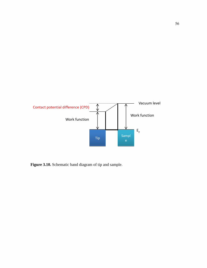
56
Figure 3.10. Schematic band diagram of tip and sample.
Tip Sampl
e
EF
Work function
Vacuum level Contact potential difference (CPD)
Work function

57
directly measured by adjusting the potential offset on the tip and keeping the first
harmonic response at zero. It is noteworthy that the signal is independent of the
geometric properties of tip-surface system and the modulation voltage [16].
3.4 Scanning Tunneling Microscopy
Scanning Tunneling Microscopy (STM) is widely used to obtain atomic-
resolution images of surfaces. It provides a three-dimensional topographic profile of a
surface, and the image inherently contains a local electronic structure of the surface. STM
operates on a phenomenon known as quantum tunneling. When a sharp metal tip, often
made of Pt or W, is brought sufficiently close to the sample surface, the electrons in the
sample can tunnel into or out of a tip to the application of a bias voltage. The resulting
current, I, is given in
∗
(3.8)
where z is the sample-tip separation, ρt is the density of state of tip, ρs is the density of
state of sample, and C is a constant [14]. The tunneling current is directly proportional to
the number of states on the sample surface. This number depends on the local density of
states of states (LDOS) at the Fermi level [17]. The LDOS is the number of electrons per
unit volume per unit energy, at a given point in space and at a given energy. To produce
images, the STM can be operated in two modes as shown in Figure 3.11. In constant
current imaging, a feedback mechanism is enabled that maintains a constant current while
a constant bias is applied between the sample and tip. These conditions require a constant
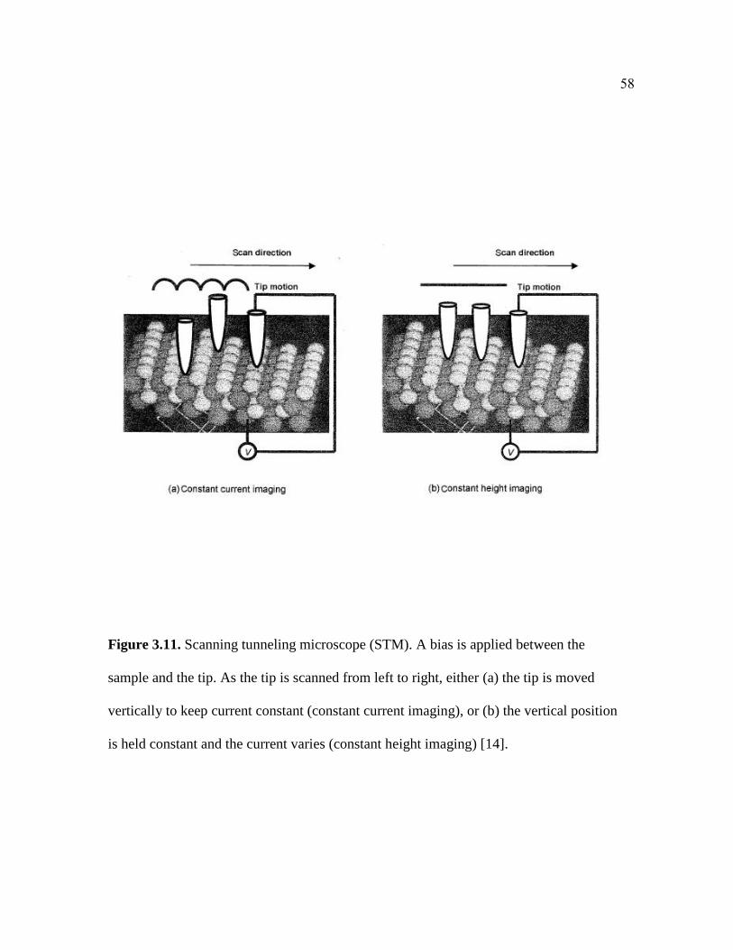
58
Figure 3.11. Scanning tunneling microscope (STM). A bias is applied between the
sample and the tip. As the tip is scanned from left to right, either (a) the tip is moved
vertically to keep current constant (constant current imaging), or (b) the vertical position
is held constant and the current varies (constant height imaging) [14].

59
sample-tip separation when the material is of constant composition. The voltage signal
required to alter the vertical tip position is used to form the image, which represents a
constant charge density contour of the surface. An alternative imaging mode is constant
height operation, in which constant tip height and constant applied bias are
simultaneously maintained. Only constant current imaging was used in this study [18].
3.4.1 Scanning Tunneling Spectroscopy
Constant-current topographs are often utilized to reveal electronic structure
information, but separating the contributions of electronic and geometric structure is not
straight-forward. The most common way of obtaining quantitative spectroscopic
information in the STM is scanning tunneling spectroscopy (STS) [17]. The STS
technique provides information about the electronic structure of the sample by probing
the sample density of states as a function of energy with atomic spatial resolution. STS
involves superimposing a small, high-frequency sinusoidal modulation voltage Vmodωmod
on top of the constant dc bias Vdc between sample and tip. The ac component of the
tunneling current is measured with a lock-in amplifier, with the in-phase component
directly giving dI/dV simultaneously with the sample topography. At lower bias voltages
(when Vdc is lower than the sample and tip work functions), structure in dI/dV as a
function of Vdc is associated with the surface density of states. The interpretation of these
low-bias dI/dV measurements is generally based on the Wentzel-Kramers Brillouin
(WKB) approximation [19]. The WKB theory predicts that the tunneling current is given
by
(3.9)

60
where ρs(r, E) and ρt(r, E) are the density of states of the sample and tip at location r and
energy E, measured with respect to their individual Fermi levels [19]. Differentiating that
equation with respect to voltage gives
(3.10)
The first term in Eq.(3.10) is the product of the density of states of the sample, the density
of states of the tip, and the tunneling transmission probability T. Although the tunneling
transmission probability, T, is usually unknown, at any fixed location T increases
smoothly and monotonically with the applied voltage V in the WKB approximation [19].
Therefore, the measured dI/dV is directly proportional to the density of states of the
sample as a function of energy at any particular location on the surface.

61
References
[1] S. Hufner, Photoelectron Spectroscopy: Principles and Applications, 3rd. ed.
Springer, 2003.
[2] D. Briggs and M. P. Seah, Practical Surface Analysis, 2nd ed. New Delhi:
Thomson Press, 1990, pp. 51–59.
[3] Z. Liu, “Modifications of Electronic and Chemical Properties of GaSb for Device
Applications,” University of Wisconsin, 2004.
[4] B. Feuerbacher, B. Fitton, and R. F. Willis, Photoemission and the Electronic
Properties of Surface. New Tork: Wiley, 1978.
[5] M. P. Seah and W. A. Dench, “Quantitative electron spectroscopy of surface: A
standard data base for electron inelastic mean free paths in solids,” Surface and
interface analysis, vol. 1, pp. 2–11, 1979.
[6] R. T. Poole, J. Liesegang, R. C. G. Leckey, and J. G. Jenkin, “A high intensity U.V.
source for photoelectron spectroscopy,” Journal of electron spectroscopy and
related phenomena, vol. 5, no. 1, pp. 773–782, 1974.
[7] J. J. Uhlrich, “Surface Chemistry and Electronic Properties of GaN and ZnO for
use in Organic/Inorganic Hybrid Electronic Devices,” University of Wisconsin-
Madison, 2009.
[8] E. I. Toh, M. I. Wamoto, M. B. Urghard, and S. R. Oth, “Ultraviolet Photoelectron
Spectroscopy and Surface Potential of π -conjugated Langmuir-Blodgett Films on
Gold Metal Electrode,” Applied Physics, vol. 39, no. 9, pp. 5146–5150, 2000.
[9] D. M. Delongchamp, E. K. Lin, and D. A. Fischer, “Organic semiconductor
structure and chemistry from Near-edge X-ray absorption fine structure
( NEXAFS ) spectroscopy .”
[10] K. Kummer, D. V. Vyalikh, G. Gavrila, A. B. Preobrajenski, A. Kick, M. Bönsch,
M. Mertig, and S. L. Molodtsov, “Electronic structure of genomic DNA: a
photoemission and X-ray absorption study.,” The journal of physical chemistry. B,
vol. 114, no. 29, pp. 9645–52, Jul. 2010.
[11] J. Stohr, NEXAFS spectroscopy. Springer-Verlag, 1996.

62
[12] D. Solomon, J. Lehmann, J. Kinyangi, B. Liang, K. Heymann, L. Dathe, K. Hanley,
S. Wirick, and C. Jacobsen, “Carbon (1s) NEXAFS Spectroscopy of
Biogeochemically Relevant Reference Organic Compounds,” Soil Science Society
of America Journal, vol. 73, no. 6, p. 1817, 2009.
[13] H. J. Butt, K. Graf, and M. Kappl, Physics and Chemistry of Interfaces. Weinheim:
Wiley-VCH, 2003.
[14] D. A. Bonnell and B. D. Huey, “Basic Principles of Scanning Probe Microscopy,”
in Scanning Probe Microscopy and Spectroscopy: Theory, Techniques, and
Applications, 2nd ed., D. Bonnell, Ed. Wiley-VCH, 2001, pp. 7–42.
[15] W. Melitz, J. Shen, A. C. Kummel, and S. Lee, “Kelvin probe force microscopy
and its application,” Surface Science Reports, vol. 66, no. 1, pp. 1–27, Jan. 2011.
[16] S. V. Kalinin and D. A. Bonnell, “Electrostatic and Magnetic Force Microscopy,”
in Scanning Probe Microscopy and Spectroscopy: Theory, Techniques, and
Applications, 2nd ed., D. A. Bonnell, Ed. Wiley-VCH, 2001, pp. 205–251.
[17] H. J. W. Zandvliet and A. van Houselt, “Scanning tunneling spectroscopy.,”
Annual review of analytical chemistry, vol. 2, pp. 37–55, Jan. 2009.
[18] C. J. Chen, Introduction to Scanning Tunneling Microscopy. Oxford: Oxford
University Press, 1993.
[19] R. J. Hamers and D. F. Padowitz, “Methods of Tunneling Spectroscopy with the
STM,” in Scanning Probe Microscopy and Spectroscopy: Theory, Techniques, and
Applications, 2nd ed., D. Bonnell, Ed. Wiley-VCH, 2001, pp. 59–110.
[20] S. M. Sze and K. K. Ng, Physics of semiconductor devices, 3rd ed. Wiley-
interscience, 2007, pp. 33–35.
[21] L. Van der Pauw, “A method of measuring specific resistivity and Hall effect of
discs of arbitrary shape,” Philips Research Reports, vol. 13, pp. 1–9, 1958.

63
Chapter 4
DNA immobilization on sulfur-passivated InAs
surfaces
4.1 Introduction
Single-stranded DNA (ssDNA) immobilized on solid surfaces has become
important in biotechnology applications such as DNA microarrays [1,2] and biosensors
[1,3]. Previous research on DNA-modified surfaces has largely explored functionalized
gold [4–7], oxidized silicon or glass surfaces [8–10]. The desire to integrate biosensors,
based on surface DNA, with preexisting electronic devices and circuits [11] requires the
immobilization of DNA on various semiconducting materials [12]. III-V semiconductors,
such as GaAs and InAs, can provide advantages in such applications over Si due to their
differing surface chemistry, band structure and electronic properties [13]. Recent studies
have shown that such III-V semiconductors can be effectively used in chemical and
biological sensing applications [14–16]. Among III-V materials, indium arsenide (InAs)
has a number of potential advantages as a substrate for DNA immobilization. InAs

64
possesses a Fermi level at the surface typically positioned above the conduction band
edge. This Fermi level position leads to the presence of a two-dimensional electron gas
(2DEG) or electron accumulation layer at the surface. This electron accumulation layer
can be modulated by surface treatments allowing InAs to serve as a useful and sensitive
sensing platform [17,18]. A variety of specific experimental stimuli can lead to changes
in the surface band bending that alter electron accumulation or depletion, including
surface defects [19,20], surface adsorption of gas molecules [21], or surface treatments
with inorganic [14,22,23] and organic molecules [24,25]. This sensitivity suggests that
InAs could be an excellent sensing platform.
Recently, surface passivation of InAs has been investigated using ammonium
sulfide ((NH4)2Sx) [26], thioacetamide [27] and methyl-terminated alkane thiols [24].
Such passivation techniques, which can change or alter service dates or provide a
chemical layer which prevents reaction with an ambient, can remove surface oxides and
other contaminants by creating a covalently bonded sulfur layer with good short-term
stability in ambient air and aqueous solutions. Although aspects of InAs surface
passivation have been investigated, functionalization with single-stranded DNA (ssDNA)
has been left unexamined on InAs surfaces despite its potential utility as an electronic
biosensor. In this chapter, a study of the immobilization of DNA on sulfur-passivated
InAs surface is presented as the basis of a nucleic-acid affinity-based sensing platform.
The sulfur passivation removes the native oxide layer of InAs and produces a stable
substrate for DNA functionalization. A comparison of the chemical characteristics of the
DNA immobilized InAs surfaces with and without sulfur-passivation using XPS

65
measurements is presented. The fluorescence measurements are used in order to
determine the effect of sulfur passivation on DNA immobilization. The electronic
properties of a ‘clean’ surface and sulfur-passivated surface are also presented.
4.2 Experimental
An aqueous solution of 20% ammonium sulfide ((NH4)2S) was used to prepare
the sulfur-passivation solutions. The solution was diluted by two parts of water for sulfur
passivation. Prior to passivation, InAs (100) samples (S-doped, n-type) were degreased in
trichloroethylene, acetone, and methanol, and cleaned with buffered oxide etch (BOE).
The etched InAs was rinsed with deionized water and soaked in the diluted ammonium
sulfide solution for 15 min at 35 °C. The samples were then rinsed under flowing
deionized water and blown dry under nitrogen. The thiolated ssDNA probe used in this
study consists of a 25-base oligonucleotide with the following sequence:
CCTCTGACTTCAACAGCGACACCCA. To verify the existence of DNA on the
surface, the 3’ end of the ssDNA was modified with fluorinated adenosine (A). The
fluorine atom at the end of the DNA probes can be detected by XPS. For fluorescence
measurements, the 3’ end of the DNA probe was modified with fluorescence dye Cy3.
The surface functionalized with ssDNA was prepared by soaking the sulfur-passivated
InAs in 2.0µM solution of DNA probes in tris-ethylenediaminetetraacetic acid(EDTA)
(TE) buffer for 20 hours. Before analysis, each sample was rinsed with deionized water
and dried with nitrogen. XPS and UPS scans were taken once the sample was transferred
into the vacuum chamber. A survey scan, as well as individual scans of the In 3d, As 3d,

66
S 2p, N 1s and F 1s core levels, were measured using the Al Kα (1486.6 eV) as an
excitation source. The measurements were performed at 15° off from the normal to the
surface (take off angle (TOA) is 75°). The core level positions and intensities were
acquired by background subtraction and fitting to a Gaussian line shape. Valence band
spectra were acquired using the He I (21.21 eV). The position of the valence band
maximum (VBM) was determined with respect to the Fermi level by linear regression at
the high kinetic energy spectral edge. The Fermi level energy of the system had
previously been located using a similar method using a sputtered gold sample.
4.3 Results and Discussion
4.3.1 Sulfur passivation
We have initially prepared sulfur passivation of InAs using ammonium sulfide
solutions ((NH4)2S) before functionalization with thiolated DNA probes. The electronic
properties of clean and sulfur-passivated InAs surfaces were investigated using ultraviolet
photoelectron spectroscopy (UPS). The surface states originate from atoms on the surface
of a crystal that cannot achieve their full coordination, leaving potentially unsaturated or
‘dangling’ bonds at the surface. Clean InAs shows surface accumulation layers that are
induced by the donor-like surface defects and the density of states are drastically
modulated by the surface reconstructions [21]. Surface treatments such as passivation
would have a large effect on the surface state energies and densities and the resultant
surface band-bending of samples. Figure 4.1 shows the UPS valence band spectra for
clean and sulfur-passivated InAs surfaces. The position of the valence band maximum

67
(VBM) was determined with respect to the Fermi level by linear regression at the high
kinetic energy spectral edge. A clean InAs surface was prepared for comparison by Ar+
sputtering at 300 eV followed by annealing at 320 °C, resulting in the InAs(100)-4x2
surface [20,26]. The Fermi level for the clean surface is located ~0.6 eV above the VBM.
Considering the band gap of InAs is 0.36 eV at room temperature, the bands of the InAs
surface are bent downward, implying formation of surface electron accumulation layer.
King et al [28] has reported that a surface band gap differs from its value in the bulk of
the material due to many-body interactions, however it was measured on the InAs (111)B
surface. The generalization of this value to the InAs (100) In-terminated surface is
uncertain. Therefore, EF is located ~0.24 eV or more above the CBM, assuming a
potentially smaller surface band gap, which is good agreement with the position derived
from core level analysis [20,29]. A small peak is seen at the same as Fermi level, and this
had been identified elsewhere [30] as emission from filled states at the conduction band
minimum. For the sulfur-adsorbed InAs surface, the strong bands disappeared around 2.0
eV below EF. The peak would be ascribed to dangling bonds on In atoms and this result
implies that the ‘dangling’ bonds on In atoms react with the sulfur and such states are no
longer at the same position relative to the band edges [26].
Quantitative chemical characterization was obtained from XPS measurement.
Table 4.1. shows the resulting normalized peak intensities of XPS analysis for sulfur-
passivated InAs. The core-level peaks have been normalized to the bulk component of As
3d peak. The observed sulfur peak of the passivated sample indicates that the sulfur
passivation was accomplished. The In-S bond was observed with negligible amount of
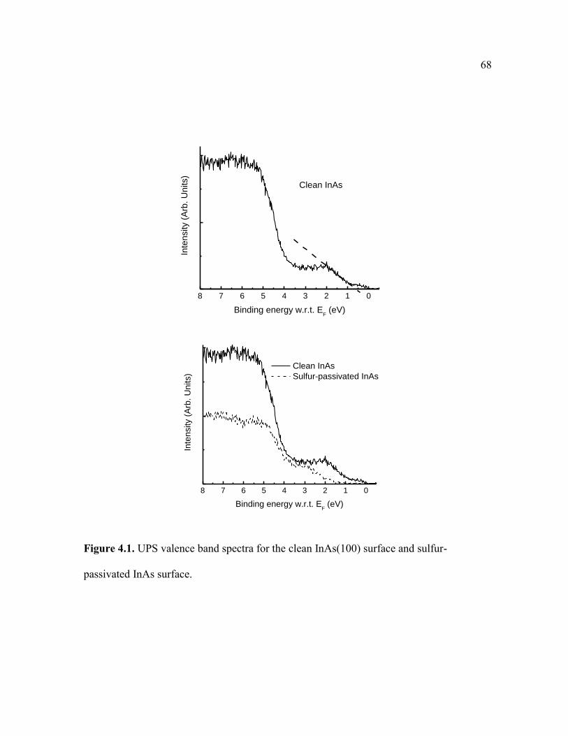
68
8 7 6 5 4 3 2 1 0
Inte
nsity (
Arb
. U
nits)
Binding energy w.r.t. EF (eV)
Clean InAs
8 7 6 5 4 3 2 1 0
Inte
nsity (
Arb
. U
nits)
Binding energy w.r.t. EF (eV)
Clean InAs
Sulfur-passivated InAs
Figure 4.1. UPS valence band spectra for the clean InAs(100) surface and sulfur-
passivated InAs surface.

69
Table 4.1. Normalized* intensities of XPS peaks for the sulfur-passivated InAs.
Core-levels Components S-passivated InAs
In 3d
In-As 1.5
In-S 0.12
In-Ox 0.13
As 3d
As-In 1.0
As-Ox -
N 1s
0.56
S 2p
0.27
F 1s
-
*For each sample, the peaks have been normalized to the bulk component of As 3d.

70
As-S bond on the passivated surface. Along the (100) direction, InAs is composed of
alternating In and As planes. In XPS data of sulfur-passivated sample, In-S bonding is
clearly observed, with no As-S. Also, it is noted that the sulfur passivation resulted the
In-rich surface. These results imply that the S displaces the surface As which may be
understandable given the substantially higher bond strength of the In-S bond [4]. This can
also be rationalized by solubility of components. AsOx and AsSx are more soluble at high
pH and InSx, AsOx and InOx are soluble at low pH [14]. Since the pH of ammonium
sulfide solution is around 10, AsOx and AsSx should be dissolved in the solution. In
addition, a nitrogen peak was observed on the sulfur-passivated InAs surface. The
nitrogen peak is due to the residual chemical of ammonium sulfide which was used for
the passivation.
4.3.2 Effect of Sulfur passivation on DNA immobilization
We have explored the functionalization with DNA probes after sulfur passivation
of the InAs surface. For comparison, we also examine a sample functionalized with DNA
probe without sulfur passivation. For fluorinated DNA probes, the fluorine signal is of
interest. Ideally, the thiolated DNA molecules interact with the surface exclusively
through the sulfur atom of the thiol group, and are vertically positioned on the surface
presenting the fluorine at the outermost surface. Table 4.2. shows the resulting
normalized peak intensities of XPS analysis for DNA-functionalized samples without and
with sulfur passivation. The observed fluorine and nitrogen peaks indicate the presence of
the DNA probes on the surface. While a small fluorine 1s XPS peak was observed for
functionalization without sulfur passivation, the signal-to-noise associated with this peak
71
is too low to allow any chemical shifts or quantitative measurement of the peak intensity
to be determined. In contrast, the XPS data obtained from samples functionalized sample
after sulfur passivation reveals a clearly resolved fluorine peak. Since DNA probes
contain large numbers of nitrogen atoms, an increase in the nitrogen peak intensity was
observed as well on the surface. These observations imply that a higher density of DNA
probes were present on the surface as compared with the sample without passivation.
In the XPS data for the functionalized InAs with sulfur passivation (Table 4.2) the In-S
bonding is clearly observed with little or no As-S. Note that the In-S bonding can be
originated either elemental sulfur from sulfur passivation or thiol of DNA probe. Even
though the sulfur passivation results in higher surface coverage of DNA probes, the S 2p
peak and In-S peak intensities were comparable to those obtained from the sulfur
passivated InAs sample. The observation of these peaks indicates that the DNA probes
are not vertically oriented with respect to the surface but may lie parallel to the InAs
surface. If DNA probes are vertically oriented on the surface, there would be a reduced
sulfur signal due to signal attenuation by the attached ssDNA.
Additional information on the functionalized sample was obtained from XPS
spectra of As 3d core-levels, shown in Figure 4.2. The corresponding As 3d XPS
spectrum immediately after passivation (Fig. 4.2 (a)) shows that there is a negligible
amount of As-Ox (BE ˜ 44-45 eV) and As-S (BE ˜ 42 eV). However, a measurable As-
Ox component, indicated by the dashed line in Fig. 4.2 (b), was observed after exposure
to the aqueous DNA functionalization solution for 20 hours. The result indicates that the
sulfur passivation does not completely suppress the oxidation of InAs during the

72
Table 4.2. Normalized intensities of XPS peaks for the functionalized InAs without and
with sulfur passivation.
Peak
Normalized Intensity*
Functionalization
w/o sulfur passivation
Functionalization
after sulfur passivation
In 3d
In-As 1.1 1.9
In-S 0.05 0.14
In-Ox 0.08 0.10
As 3d
As-In 1.0 1.0
As-Ox - 0.21
N 1s 0.18 2.5
S 2p 0.08 0.26
F 1s 0.02 0.50
*For each sample, the peaks have been normalized to the bulk component of As 3d.

73
functionalization procedure. While the DNA functionalization occurs, the sample is
soaked in the aqueous solution. Such condition may cause the oxidation of As.
The fluorescence measurements also confirm a higher coverage of ssDNA on the sulfur-
passivated surfaces as compared to the sample without passivation. The image of
functionalized samples was processed with ‘ImageJ’ software [9] to subtract the
background signal. The images of etched and non-functionalized InAs surface were taken
under the same magnification and exposure time, and were used as a measure of the
background signal. The population and distribution of DNA probes on the surface was
significantly more uniform by sulfur passivation before functionalization. Quantitatively,
the mean fluorescent intensity is a measure of the areal concentration of DNA probes on
surface. The mean intensity of the functionalized sample without passivation is 59.43
with standard deviation of 4.83, and that with passivation is 67.32 with standard deviation
of 5.29. The higher intensity value confirms that the DNA probes were immobilized on
the surface with high areal density when the surface was passivated with sulfur prior to
DNA functionalization.

74
(a)
34 36 38 40 42 44 46 48
Binding energy (eV)
(b)
34 36 38 40 42 44 46 48
Binding energy (eV)
Figure 4.2. XPS of As 3d core-level spectra for InAs surfaces. (a) The sample after sulfur
passivation shows As-In (BE = 40.9 eV) peak with negligible amount of As-Ox (BE = 44-
45 eV) and As-S (BE ≈ 42 eV). (b) The sample after functionalization of passivated
surface shows not only As-In but also As-Ox, indicated by the dashed line.

75
4.4 Conclusions
The surface chemical composition and electronic states of InAs(100) passivated
with sulfur were investigated using XPS, UPS and fluorescence measurements. UPS
spectra show that the Fermi level of the clean InAs surface is ~0.24 eV above the CBM,
implying formation of the accumulation layer. The surface states were changed by sulfur
passivation and it suggested that the In-based surface states participate in the sulfur
reaction leading to its incorporation into the surface layer. The DNA-functionalized InAs
surface with and without sulfur passivation were compared using XPS and fluorescence
measurements. These measurements suggest that the sulfur-adsorbed InAs surface
possess a higher density of DNA immobilized on the surface when compared with the
functionalized sample without sulfur passivation. The functionalized surfaces showed the
sulfur peak as much as that observed on the sulfur-passivated surface indicating that the
DNA probe is not vertically oriented on the surface. Also some oxidation of surface As
after DNA functionalization was found indicating that the passivated surface could not
perfectly restrain the surface from re-oxidation while the functionalization occurs.

76
References
[1] J. Wang, Nucleic acids research 2000, 28, 3011–6.
[2] B. P. Nelson, T. E. Grimsrud, M. R. Liles, R. M. Goodman, R. M. Corn, Analytical
chemistry 2001, 73, 1–7.
[3] N. Chaniotakis, N. Sofikiti, Analytica chimica acta 2008, 615, 1–9.
[4] D. Y. Petrovykh, H. Kimura-Suda, L. J. Whitman, M. J. Tarlov, Journal of the
American Chemical Society 2003, 125, 5219–26.
[5] a G. Frutos, Q. Liu, a J. Thiel, a M. Sanner, a E. Condon, L. M. Smith, R. M. Corn,
Nucleic acids research 1997, 25, 4748–57.
[6] D.-W. Pang, M. Zhang, Z.-L. Wang, Y.-P. Qi, J.-K. Cheng, Z.-Y. Liu, Journal of
Electroanalytical Chemistry 1996, 403, 183–188.
[7] K. Hashimoto, K. Ito, Y. Ishimori, Analytical chemistry 1994, 66, 3830–3.
[8] M. Yang, R. Y. C. Kong, N. Kazmi, A. K. C. Leung, Chemistry Letters 1998, 257–
258.
[9] E. Souteyrand, J. P. Cloarec, J. R. Martin, C. Wilson, I. Lawrence, S. Mikkelsen,
M. F. Lawrence, The Journal of Physical Chemistry B 1997, 101, 2980–2985.
[10] J. B. Lamture, K. L. Beattie, B. E. Burke, M. D. Eggers, D. J. Ehrlich, R. Fowler,
M. a Hollis, B. B. Kosicki, R. K. Reich, S. R. Smith, Nucleic acids research 1994,
22, 2121–5.
[11] T. Vo-Dinh, J. P. Alarie, N. Isola, D. Landis, a L. Wintenberg, M. N. Ericson,
Analytical chemistry 1999, 71, 358–63.
[12] T. Strother, R. J. Hamers, L. M. Smith, Nucleic acids research 2000, 28, 3535–41.
[13] F. Seker, K. Meeker, T. F. Kuech, A. B. Ellis, Chemical reviews 2000, 100, 2505–
2536.
[14] D. Y. Petrovykh, M. J. Yang, L. J. Whitman, Surface Science 2003, 523, 231–240.
[15] R. Flores-Perez, D. Y. Zemlyanov, A. Ivanisevic, Chemphyschem: a European
journal of chemical physics and physical chemistry 2008, 9, 1528–30.

77
[16] L. Mohaddes-Ardabili, Journal of Applied Physics 2004, 95, 6021.
[17] D. Tsui, Physical Review Letters 1970, 24, 303–306.
[18] S. Bhargava, H.-R. Blank, V. Narayanamurti, H. Kroemer, Applied Physics Letters
1997, 70, 759.
[19] L. Piper, T. Veal, M. Lowe, Physical Review B 2006, 73, 195321.
[20] M. Håkansson, L. Johansson, C. Andersson, U. Karlsson, L. Ö. Olsson, J. Kanski,
L. Ilver, P. Nilsson, Surface science 1997, 374, 73–79.
[21] M. Lowe, T. Veal, C. McConville, G. Bell, S. Tsukamoto, N. Koguchi, Surface
science 2003, 523, 179–188.
[22] Y. Watanabe, F. Maeda, Applied surface science 1997, 117, 735–738.
[23] L. Giovanelli, N. Papageorgiou, G. Terzian, J. M. Layet, J. C. Mossoyan, M.
Mossoyan-Deneux, M. Göthelid, G. Le Lay, Journal of Electron Spectroscopy and
Related Phenomena 2001, 114-116, 375–381.
[24] D. Y. Petrovykh, J. C. Smith, T. D. Clark, R. Stine, L. a Baker, L. J. Whitman,
Langmuir 2009, 25, 12185–94.
[25] T. a. T. Tanzer, P. W. Bohn, I. V. Roshchin, L. H. Greene, J. F. Klem, Applied
physics letters 1999, 75, 2794.
[26] Y. Fukuda, Vacuum 2002, 67, 37–41.
[27] D. Y. Petrovykh, J. M. Sullivan, L. J. Whitman, Surface and Interface Analysis
2005, 37, 989–997.
[28] P. King, T. Veal, C. McConville, J. Zúñiga-Pérez, V. Muñoz-Sanjosé, M.
Hopkinson, E. Rienks, M. Jensen, P. Hofmann, Physical Review Letters 2010, 104,
1–4.
[29] L. Olsson, L. Ilver, J. Kanski, P. Nilsson, C. Andersson, U. Karlsson, M.
Håkansson, Physical review. B, Condensed matter 1996, 53, 4734–4740.
[30] L. Olsson, C. Andersson, M. Håkansson, J. Kanski, L. Ilver, U. Karlsson, Physical
review letters 1996, 76, 3626–3629.

78
Chapter 5
Chemical and Electrical Characterization of
DNA-immobilized InAs surfaces using XPS, UPS
and NEXAFS
Portions of this chapter were published in “Chemical characterization of DNA-
immobilized InAs surfaces using X-ray photoelectron spectroscopy and near-edge X-ray
absorption fine structure” , by EunKyung Cho, Thomas F. Kuech, and April Brown,
Langmuir, v 28, n 32, p 11890-11898, August14, 2012.
5.1 Introduction
DNA immobilization on solid surfaces is the basis of many biotechnical
applications, such as DNA microarrays [1,2] and biosensors [1,3]. The immobilization of
DNA on InAs is interesting because InAs is one of the few semiconductors that possess a

79
surface Fermi level typically positioned above the conduction band edge [4,5]. This leads
to the presence of a quasi-two-dimensional electron gas at the surface that can be
modulated by adsorbed species and other binding events. Thus, this material is an
excellent candidate for a variety of sensing applications. The use of InAs in an electronic
device or chemical and biological sensing application requires control over the InAs
surface properties [4–8]. Surface chemical passivation of InAs, using inorganic and
organic materials, has resulted in well-defined chemical and electronic properties which
are required for sensing applications [9–11]. For example, the surface structure and
electronic states of InAs treated with ammonium sulfide solutions ((NH4)2Sx) have been
investigated [6,12]. Sulfide-based passivation removes native oxides and other
contaminants leaving a covalently-bonded sulfur layer possessing good short-term
stability in ambient air and aqueous solutions compared with non-passivated InAs. Other
sulfur-based chemical preparations have used a weakly basic solution of thioacetamide as
an alternative to inorganic sulfide passivation [9]. A study on self-assembled monolayers
(SAMs) of methyl-terminated alkanethiols has shown that these molecules are bonded to
InAs through the thiol end-groups, which were found effective in chemically and
electronically passivating the surfaces in aqueous buffer such as phosphate buffered
saline (PBS) buffer (pH 7.4) [13]. The chemical bonding of amino acids onto InAs
surfaces has also been studied and the amino acids were shown to block subsequent oxide
growth on the InAs surface depending on the type of oxides present on the surfaces as
well as the amine functional groups [14,15].

80
In this study, we have investigated the immobilization of thiolated ssDNA probes
on n-type InAs(100) surfaces. The immobilized ssDNA/InAs serves as the basis of a
nucleic acid affinity-based sensing platform. Aqueous-based chemical etches using a
weakly basic solution or diluted hydrogen fluoride were used to remove the InAs surface
oxide. The ssDNA probe was subsequently immobilized on the InAs surface using two
different functionalization approaches. X-ray photoelectron spectroscopy (XPS),
ultraviolet photoelectron spectroscopy (UPS) and near-edge X-ray absorption fine
structure spectroscopy (NEXAFS) were used to characterize the interfacial chemistry
between DNA probe and InAs substrate and polarization dependence of the ssDNA
immobilized on the InAs substrate.
5.2 Experimental
5.2.1 Materials
InAs(100) n-type, S-doped samples were cut from a single-side polished wafer
(WaferTech). The InAs samples were sequentially degreased in trichloroethylene (TCE),
acetone and methanol for 3 min. each. The samples were initially etched by soaking into
either a HF- or an NH4OH-based solution. The HF solution consisted of as-received HF
(49% HF, Honeywell) diluted in methanol to 5% volume concentration. The NH4OH
solution was prepared by 1:1 volume mixture of the 29.7% NH4OH stock solution (Fisher
Scientific) and deionized water. The InAs samples were rinsed in deionized water and

81
dried with flowing nitrogen before being transferred into an ultra-high vacuum (UHV)
chamber.
The ssDNA probes (Integrated DNA Technologies, Inc.) contained 25-base
oligonucleotides with the following sequence: 5’-HO(CH2)6-S-S-(CH2)6-
CCTCTGACTTCAACAGCGACACCCA-F-3’. The 5’ end of the probes was modified
with a C6 thiol as an anchor to the InAs surface and the 3’ end of the probe was modified
with fluoro-adenosine to verify the existence of DNA on the surface. The as-received
thiolated probes were treated with tris(2-carboxyethyl)phosphine (TCEP) solution that
served to cleave the S-S bond at the 5’ end modifier. In this case, the thiolated ssDNA
probe (HS-ssDNA) as well as HO-(CH2)6-SH (mercaptohexanol, MCH) existed in the
functionalization solution.
5.2.2 Sample preparation
The sample labeling, ‘Cxy’, in this paper is used to designate the surface
preparation, ‘x’, and functionalization procedure, ‘y’. Samples were prepared with an
etching and annealing process. All of the prepared samples are summarized in Table 1.
The as-received InAs which was rinsed with TCE, acetone, and methanol before the
etching procedure is referred to as C0, C1 and C2 samples were NH4OH etched for 10
min. or HF etched for 3 min., respectively. Both etching procedures left ~2.5 nm residual
oxide on the surface as measured through ellipsometry. C3 samples were HF etched for 3
min. and annealed at 380 °C for 10 min. in an UHV system. As a result of the annealing
process, an InAs(100)-(4x2) reconstruction was observed using reflection high-energy
electron diffraction (RHEED). The C0, C1, C2, and C3-designated samples received no

82
additional DNA treatments. To prepare the DNA-immobilized InAs, the etched InAs
samples were immersed in the functionalization solution. The functionalization solution
for CxA samples was prepared with 2μ DNA and 200μ TCEP solution in a 1:9
mixture of NH4OH (29% stock solution) in tris-ethylenediaminetetraacetic acid (EDTA)
(TE) buffer (Fluka, pH 7.4). The CxA samples were exposed to this solution for 1 hr.
with the temperature of the DNA-based solution held at 55 °C. The CxB samples were
functionalized with a solution consisting of 2μ DNA and 200μ TCEP, diluted in TE
buffer, for 17 hr. at room temperature. Each sample was rinsed with deionized water and
dried under flowing nitrogen before analysis. The prepared samples were transported and
stored in a VWR® Desi-VacTM container with automatic vacuum pump before inserting
into the XPS analysis chamber. The container provides a clean, dry environment, but
some reoxidation of the sample is expected since the vacuum in the container is ~380
Torr, which is not sufficient to keep the surface completely oxide-free. The samples were
inserted into the XPS chamber within 10 min with the exception of C3. The C3 sample
had been stored for an hour in the container before inserting into the UHV chamber.
5.2.3 XPS and UPS characterization
The surfaces were characterized using X-ray Photoelectron Spectroscopy (XPS)
with Al Kα monochromatic source and UPS with He I source (21.2 eV). XPS and UPS
measurements were carried out at room temperature in a UHV system with base pressure
of < 1 x 10⁻⁹
Torr. The background chamber was monitored using a residual gas analyzer
(Inficon Transpector), and was found to be comprised of mostly hydrogen with small
traces of nitrogen (< 5%) and water (< 2%). The high-resolution XPS scans were

83
acquired using a 30° take-off angle for the In 3d, As 3d, As 2p, C 1s, O 1s, N 1s, F 1s, P
2p and S 2p spectral regions with 20 eV pass energy. Charge correction was performed
using the adventitious C 1s peak at 285.0 eV. The peaks in the core-level spectra were fit
using the Casa XPS software, version 2.3.15 [16]. A convolution of Lorentzian and
Gaussian line shapes was used to fit the peaks. Shirley and linear functions were used to
the model the signal background [9,10,13].
5.2.4 NEXAFS characterization
Near-edge X-ray absorption fine structure (NEXAFS) spectra were taken at the
Synchrotron Radiation Center in Madison, Wisconsin using the HERMON beamline with
total electron yield detection. The base pressure of the measurement chamber was < 2 x
10-10
Torr. The X-rays were > 90% linearly polarized. For each sample, scans were taken
at the carbon K-edge region. All NEXAFS spectra were normalized by the signal from a
gold-coated 90% transmission grid placed in the path of the X-rays to eliminate the effect
of incident beam intensity fluctuations.

84
Table 5.1. Sample nomenclature
Cleaning method Functionalization solution
C0 -
-
C1 NH4OH etch
C2 HF etch
C3 HF etch and anneal at
380 °C
C1A NH4OH etch
HS-ssDNA/MCH in a 1:9 mixture of NH4OH
in TE C2A HF etch
C3A HF etch and anneal at
380 °C
C1B NH4OH etch
HS-ssDNA/MCH in TE C2B HF etch
C3B HF etch and anneal at
380 °C

85
5.3 Results and Discussion
5.3.1 XPS analysis of clean InAs surfaces
Prior to functionalization, the native oxide was removed. The C0, C1, C2, C3
samples were prepared as summarized in Table 5.1 and were characterized as a reference
for the DNA-functionalized InAs surfaces. Figure 5.1 presents the As 3d and In 3d
spectra of the as-received and differentially-cleaned surfaces. The As 3d spectrum of the
as-received sample (C0) was resolved into As-In (40.6 eV), elemental arsenic (41.2 eV),
As2O3 (43.7 eV) and As2O5 (45.1 eV) peaks. The In 3d spectrum of sample C0 contains
contributions from the In-As (444.1 eV) and In-Ox (445.0 eV) peaks. The separation of
binding energies (BE) between the In-As and In-oxide components is found to be ~0.85
eV for sample C0. In fitting the spectra of C1, C2 and C3, the same BE separation was
used to deconvolve the spectral features. As shown in Fig. 5.1, the area under the oxide
components in the As 3d and In 3d XPS spectra was significantly lower for both etched
samples (C1 and C2) when compared to the native InAs sample (C0), indicating that
there was substantial removal of the outer oxide layer. The HF-etching (C2) was found
to be the most effective in oxide removal. The as-received sample, C0, possessed two
forms of arsenic oxide: As2O3 and As2O5. The As2O5 peak was not observed after use of
either etching procedures (C1 and C2), but a small amount of As2O3 remained on the
surface. Since the samples were exposed to air (less than 5 min.) between etching and
XPS analysis, some re-oxidation of the etched samples could be expected. After
annealing, the As2O5 peak at ~ 45 eV reappeared, in addition to the previously found
As2O3 component in the As 3d spectrum of C3, with overall increases in the residual

86
oxides noted in the In 3d and As 3d spectra. Although the annealing procedure was
carried out at 380 °C under UHV conditions and a InAs(100)-(4x2) reconstruction was
observed, the annealing temperature was not high enough to desorb all the residual
arsenic oxide on the surface [17]. Considering the reaction, As2O5 → As2O3 + O2, occurs
below 300 °C [18], the As2O5 should not be have been found after the annealing
procedure. However, an increase in the As2O5 and indium oxide was observed in the XPS
spectra of the C3 sample may be attributed to the longer air-exposure of the sample as
compared to the C1 and C2 samples. A thicker initial oxide is therefore not completely
removed. In addition, higher annealing temperatures, while desorbing the oxide, leads to
preferential As loss and a resulting In-rich surface. The In-to-As ratio calculated based on
the area of In 3d and As 3d spectra was found to be 1.2 for C1 and C2 and 1.3 for C3.
The As loss was not therefore not considered significant at the employed annealing
temperature of 380 °C.
5.3.2 Immobilized DNA on InAs surfaces
The chemically prepared substrates, C1, C2, and C3, were soaked in the DNA
solution to immobilize the DNA probes on InAs surface. Samples of C1A, C2A, C3A,
C1B, C2B, and C3B were differed by the functionalization method. InAs substrate
elements (In 3d and As 3d) and ssDNA probe components (F 1s, N 1s, and P 2p) were
examined using high-resolution XPS. Figure 5.2 presents the F 1s, N 1s, and P 2p core
level spectra of the functionalized InAs. The fluorine peak is not attenuated by the
deposited molecules on the surface since fluorine exists in the 3’ end of DNA probe,
indicating that the ssDNA was immobilized and attachment was through the thiol.

87
38 40 42 44 46 48
C3
C2
C1
As3d
C0
BE (eV)
442 444 446 448
C3
C2
C1
C0
In3d5/2
BE (eV)
Figure 5.1. As 3d and In3d5/2 spectrum of as-received and cleaned InAs samples: as-
received InAs sample (C0); NH4OH-etched InAs (C1); HF-etched InAs (C2); HF-etched
and annealed InAs (C3). The annealing step was carried out in UHV at 380oC. A doublet
separation of 0.69 eV for As 3d region and 7.55 eV for In 3d region was used and spin-
orbit splitting intensity ratio was 0.67 for both spectra.

88
DNA immobilization on the surfaces can also be confirmed by the presence of nitrogen
from the nucleobases and phosphorus from the phosphate backbone. The N 1s spectrum
was resolved into two peak components with BEs of ~399.3 eV and ~400.8 eV. The BE
of the N 1s peaks is consistent with published results [19] found for immobilized ssDNA
with a mixture of 4 bases (A, T, C, G) on gold. The N 1s component with higher BE is
attributed to bases containing an NH2 group, while the lower BE peak is due to the imino
species which include N=C bonds [20]. The P 2p core level was observed at a BE of
~134.0 eV. Since the P 2p region is adjacent to the As 3p region of the InAs, we used a
‘Tougaard’ background estimation for the P 2p peak. The experimental P-to-N atomic
ratios, calculated from the XPS peak area of N 1s and P 2p, were found to be 0.3-0.4. The
stoichiometric ratio of P/N based on the DNA probe molecule is 0.3 and is similar to the
experimentally derived values. The higher experimental ratio of P/N could be due to an
over-estimation of the area of P 2p spectrum. It is interesting to note that the amount of
DNA immobilized on the surface was not affected by the cleaning method prior to the
functionalization.
Previous reports indicate that immobilized DNA can suffer x-ray radiation
damage during XPS examination, potentially affecting the present measurements and
subsequent conclusions. S. Ptasinska et al. reported that DNA can be modified under
magnesium Kα X-ray exposure leading to nucleobase damage and/or strand breaks in the
DNA molecule.[20] A strong, 50%, degradation of nucleobases as well as DNA stand
breakage was found by monitoring the O 1s, C 1s, and P 2p regions over the course of a 5
hr exposure. In the present study, breakage of the N-glycosidic bond and/or the DNA

89
675 680 685 690
BE (eV)
B3
B2
B1
A3
A2
A1
396 399 402 405
B3
B2
B1
A3
A2
A1
BE (eV)
130 132 134 136 138
B3
B2
B1
A3
A2
A1
BE (eV)
Figure 5.2. High-resolution XPS spectra of the (a) F 1s, (b) N 1s and (c) P 2p core levels
from the functionalized samples (C1A, C2A, C3A, C1B, C2B, and C3B). The N 1s
region was deconvoled into two components associated with the primary amine and
imino groups. Peak binding energies for the spectra were referenced to the adventitious C
1s component at 285.0 eV.

90
backbone would have led to a decrease in the F 1s peak area with X-ray exposure. No
decrease in the F 1s peak area was noted after continual exposure for ~10 hrs of continual
X-ray exposure. The combined use of the monochromatic Al Kα source and a resulting
lower photon flux, when compared to the conventional unmonochromatized source [21],
leads to a reduced or negligible damage to the DNA probe.
5.3.3 Interface Chemistry
The ideal truncated InAs (100) surface is terminated with either an In- plane or
As- plane possessing unsaturated or dangling bonds. Ideally, without reconstruction, the
dangling bonds of In would be empty, while those of the more electronegative As would
contain 2 electrons each. A variety of surface reconstructions will occur, however,
depending on the surface stoichiometry and temperature [22]. Many such reconstructions
provide both In and As binding sites to adsorbed molecules. Thiolate adsorption via
formation of a single covalent bond to the surface brings a single electron to the surface
altering the existing electronic balance. This adsorption event can result in new surface
states corresponding to the interaction of the thiolate and the surface atoms. The exact
nature of the S-substrate bonds formed by thiolates to III-V semiconductor surfaces has
been of continuing interest in the literature [23,24].
XPS spectra of the As 3d and In 3d peaks from the DNA-functionalized InAs
surfaces are shown in Figure 5.3. The binding energies of substrate components are
summarized in Table 5.2. The In 3d spectrum consists of peaks associated with In-As,
and In-S and/or In-Ox bonds. The BE difference between the In-S and In-Ox peaks is
~0.35 eV [10,25] which is at the limit of the resolution of the XPS measurements in this

91
39 42 45 48
C3A
C2A
C1A
BE (eV)
(a) As 3d
440 442 444 446 448
(b) In 3d
C3A
C2A
C1A
BE (eV)
39 42 45 48
C3B
C2B
C1B
BE (eV)
440 442 444 446 448
C3B
C2B
C1B
BE (eV)
Figure 5.3. High-resolution XPS spectra of the (a) As 3d and (b) In 3d5/2 region for the
functionalized InAs. A doublet separation of 0.69 eV and intensity ratio of 0.67 was used
for As 3d5/2 and As 3d3/2 peak components. Spin-orbit splitting of In 3d peaks was 7.55
eV and intensity ratio was 0.67 for the doublet.

92
Table 5.2. Binding Energy of main components for As 3d and In 3d5/2 core levels.
Binding Energy (eV)
In-As As0 As-S As2O3 As2O5 In-S In2O3
As 3d 40.7±0.1 41.2±0.1 41.6±0.1 44.0±0.1 45.3±0.1
In 3d5/2 444.2±0.1 444.7±0.1 445.0±0.1

93
study and leads to difficulties in the resolution of the individual peaks. A fixed BE
separation of 0.5 eV between the In-S and In-As components was therefore used to
deconvolve the In 3d spectrum of the functionalized samples [10]. A comparison of the
As 3d core level spectrum of the functionalized sample (Fig. 5.3) with that of clean
sample (Fig. 5.1) indicates that a significant peak appears as a shoulder on the high BE
side of the As 3d peak after DNA functionalization. This shoulder is attributed to an As-S
derived peak. The observed BE difference between the As-In and As-S component is 0.9
± 0.1 eV, consistent with other reports [10,24]. Given the reported 0.5 eV BE separation
between As-In and elemental As component [13], this As-S component is an additional
0.4 eV higher BE than the elemental As component. Therefore, the As 3d spectrum
clearly demonstrates that the BE separation of functionalized samples are characteristic
of As-S.
The In 3d and As 3d core level peaks contain both In-S and As-S components on the
functionalized surface. The ratio of (In-S)-to-(In-As) and (As-S)-to-(As-In) is
summarized in Table 5.3. These data indicate that the surface preferentially possesses As-
S bonds on CxA samples. In contrast, As-S and In-S bonds were similar amount on CxB
samples. The functionalized InAs substrates have a different surface chemistry, or bond
formation which is primarily determined by functionalization environment and not the
cleaning methods prior to DNA immobilization. Surface composition is found to play an
important role on formation of the thiolate-surface bond [26]. A difference in the type of
surface bond made by the thiolate can be expected on In versus As terminated surfaces
resulting in In-S or As-S bonds. The DNA functionalization was carried out in an

94
NH4OH solution in cases of C1A, C2A, and C3A and result in preference of As-S
bonding over In-S bonding. The reaction with a chemical environment can lead to the
disruption of a surface termination (In vs As) since the NH4OH solution strips the native
oxide from the InAs sample during functionalization [10,13]. The surface stoichiometry,
represented by the ratio of As-to-In, was calculated based on the As 3d and In 3d XPS
spectra as summarized in Table 5.3. In the case of the CxA samples, the As-to-In ratio is
larger than 1.5 showing an As-rich surface, while CxB samples possess approximately
equal atomic concentrations of As and In on the functionalized surface. The weakly basic
NH4OH solution used for the CxA samples appears to generate an As-rich surface. This
surface stoichiometry leads to the presence of dominant As atoms on the surface provides
the higher probability of binding between the thiol and As atoms, rather than In atoms. It
is worth noting that the study of alkanethiol SAMs on GaAs with predominant As-S
bonding also used NH4OH-based solution [24].
5.3.4 NEXAFS Studies
Even though the In 3d and As 3d core level peaks contain both In-S and As-S
components on the functionalized surfaces, it is unclear whether this S-substrate bond
originates uniquely from DNA probe alone. The 5’ end of DNA probe was modified with
HO(CH2)6-S-S-(CH2)6-, and the S-S bond was cleaved by TCEP into HO(CH2)6-SH
(hereafter mercaptohexanol, MCH) and HS-(CH2)6-ssDNA (hereafter HS-ssDNA). The
mercaptohexanol was not removed from the functionalization solution, and was present
along with the HS-ssDNA. NEXAFS was used to verify which molecule was
immobilized on the surface as shown in Figure 5.4. The C K-edge spectra consist of a

95
Table 5.3. XPS compositional Data for functionalized samples
Sample As-S/As-In In-S/In-As As/In
C1A 1.05 0.17 1.7
C2A 1.07 0.19 1.5
C3A 1.03 0.19 1.8
C1B 0.22 0.20 1.0
C2B 0.24 0.21 1.0
C3B 0.31 0.18 1.1

96
series of features originating from HS-ssDNA and MCH. The peak at 287.3 eV was
assigned to σ*CH [19], the peak at 288.5 eV was attributed to the σ
*CO [27,28] which is
characteristic of the MCH. The σ*CNH peak was found at 289 eV [19,29] and is
characteristic of the ssDNA alone. The C1A and C1B samples possessed σ*CH and σ
*CO
with negligible σ*CNH transition which indicates that the MCH is the dominant species
immobilized on the surface. This result was also confirmed with the NEXAFS spectrum
of C1M sample, which is treated with a MCH solution without HS-ssDNA probe. These
data indicate that both MCH and HS-ssDNA compete for the In and As bonds during
functionalization resulting in the immobilization of MCH on the surface rather than HS-
ssDNA probe.
5.3.5 Electronic Properties
Although it is generally accepted that there is a two-dimensional electron gas
(2DEG) at the InAs surface, the nature of the electronic states responsible for a Fermi
level (EF) pinning above the conduction band minimum (ECB, CBM) is a subject of
ongoing debate [30–32]. It has been reported that the EF pinning may differ for
differently prepared surfaces. For instance, the In-rich surface prepared by ion
bombardment followed by annealing showed a Fermi level pinning at 0.25 eV above the
CBM, while the molecular beam epitaxy (MBE)-prepared In-rich surface was pinned just
below the CBM.38
Moreover, the changes in the electronic state of InAs with surface
treatment had been studied. For example, the (NH4)2Sx-passivated InAs(001) grown by
MBE showed an As 3d5/2 core-level shift to a higher binding energy of about 75 meV
(downward band bending) for the passivated surface as compared with as-grown film [6].

97
288 292 296 300 304 308
Photon Energy (eV)
C1B
C1A
C1M
Figure 5.4. Carbon K-edge NEXAFS spectra for the C1A and C1B samples. The C1M
sample was only treated with MCH without DNA probe in the functionalization solution.
The σ*CH peak is positioned at 287.3 eV, the peak at 288.5 eV is attributed to the
σ*CO ,and the σ
*CNH peak is found at 289 eV.

98
The InAs(001)-(2x1) surface showed 400 meV downward band bending upon selenium
passivation demonstrated by valence band spectra in the In 4d and As 3d spectra, where
the EF position is located at about 0.15 eV above the CBM for the clean InAs(001)-(2x1)
surface [33]. The change in surface band bending or binding energy shifts upon the
treatment of InAs surfaces with organic molecules has not been reported.
The surface band bending was determined through changes in core level position
and is attributed to the changes in the surface electronic structure [33,34]. The BE of the
As-In peak in the As 3d5/2 spectra was used to determine the electronic structure of the
functionalized InAs samples. It is interesting to note that the As 3d5/2 core level position
appears to be determined by the specific DNA functionalization method (A or B)
regardless of the prior surface etching procedure as shown in Figure. 5.5. The A samples
possess a greater surface band bending by 0.13 eV when compared with the B samples.
The work function of the functionalized samples were determined from the UPS spectra.
The work function is defined as the energy needed to remove an electron from the sample
Fermi level to the vacuum level. The work function was determined through the
difference between photon energy (He I, 21.2 eV) and the secondary electron emission
edge (high energy cutoff) of UPS spectra. Figure 5.6 shows the UPS spectra and
secondary electron emission edge of the spectra for the C1A and C1B samples. The high
energy cutoff was found at similar BE for both samples implying that the work function
did not change under either functionalization procedure, A or B, and had a value of 4.95
eV.

99
A surface dipole associated with In-S and As-S bonds can lead to a variation in
electron affinity as well as in the surface state density and position. Surface states can
generally arise from changes in the surface composition, surface defects, and introduced
states by adsorbed species [6]. It is therefore often difficult to ascribe a specific
underlying cause of the changes attributed to surface states. Since the work function is
similar for both C1A and C1B samples, any electron affinity change caused by a surface
dipole layer must be negligible. The realized surface band bending was therefore
primarily determined by the DNA functionalization method.
Two factors impact the dependence of surface state density on the DNA
functionalization process. The functionalization process can change surface composition.
The surface stoichiometry, represented by the ratio of As-to-In, was shown in Table 5.2.
In the case of the A samples, the As-to-In ratio is larger than 1.5 indicating an As-rich
surface, while the B samples possess approximately equal atomic concentrations of As
and In on the functionalized surface. The charge density of the As-terminated surface has
been reported to be an order of magnitude higher than on the In-terminated surface [31].
L. O. Olsson et al. confirmed this observation by showing that the EF pinning position is
different on the InAs(001)-(4x2) and -(2x4) surfaces, which are terminated by In and As,
respectively [32]. The EF on the 2x4 surface was pinned well above the CBM, but the EF
on the 4x2 surface was very close to the CBM. The As-rich surface is expected to be a
disordered surface after the wet procedure used in the type ‘A’ DNA functionalization.
The comparison of the absolute charge density of these samples with a well-ordered InAs
surface may therefore not be meaningful. The various changes in surface composition,

100
Figure 5.5. The binding energy of As-In component in the As 3d5/2 core-level for DNA
functionalized InAs samples.
40.50
40.55
40.60
40.65
40.70
40.75
40.80
40.85
40.90
40.95
41.00
C1A C2A C3A C1B C2B C3B
Bin
din
g E
ner
gy o
f A
s 3d
5/2

101
18 15 12 9 6 3 0 18 17 16 15
Inte
nsity [a.u
.]
BE w.r.t. EF (eV)
C1A
C1B
(a)
Inte
nsity [a.u
.]
BE w.r.t. EF (eV)
(b)
Figure 5.6. (a) UPS spectra and (b) secondary electron emission edge of the spectra for
the C1A and C1B. The high energy cutoff was found at 16.25 eV for the C1A and C1B
samples.

102
resulting from the type of functionalization procedure, can be one of the reasons for the
changes in surface band bending.
The surface roughness can also affect the surface band bending [35]. The surface
roughness of C1A and C1B was measured by AFM. The root-mean-square (rms)
roughness of the C1A and C1B surfaces was 1.2-1.3 nm. This measured surface
roughness results from a combination of both the etch-preparation and the DNA
immobilization process. Samples were also examined that were treated under the same
conditions as C1A and C1B but without the DNA probe in the solution in order to gauge
the contribution of the DNA itself to the observed surface morphology. The C1A sample,
so treated, exhibited a smoother surface morphology than the C1B sample. The rms
roughness was 2.6 nm for the C1A surface and 3.1nm for the C1B surface both without
DNA. The surface roughness can alter the density and distribution of surface states
resulting in localized surface charges [36]. Since the surface roughness is directly related
to the surface functionalization method, the trend observed in the electronic properties of
C1A and C1B samples may be due, in part, to such roughness-derived trapped charges in
combination with the DNA attachment.

103
5.4 Conclusions
The chemical and electronic characterization of DNA immobilized InAs surfaces
was studied by XPS, UPS and NEXAFS measurements. Before the DNA
functionalization, the effect of HF- and NH4OH- based etches on the surface oxide
removal and pre-functionalization surface chemistry was determined. The DNA
functionalization was compared using two methods, method ‘A’ used a DNA solution
containing ammonium hydroxide and method ‘B’ used a TE-based DNA solution. The
interface chemistry of the functionalized surfaces revealed that both As-S and In-S
bonding formed on the surface. The As 3d and In 3d core level spectra showed that the
CxA samples have predominant As-S bonding on the As-rich surface, while the CxB
samples had similar amount of In-S and As-S components on the surface. The NEXAFS
study demonstrated that many of As-S and In-S bonds on the surface do not originate
from the thiolated DNA probe, but from the mercaptohexanol molecule that is also
present in the functionalization solution. The functionalization environment also affected
the electronic properties of the functionalized surfaces. The BE of As 3d core-level of the
CxA samples was 0.13 eV higher compared with the CxB samples, and work function for
both samples were found to be the same which was determined by UPS spectra. The CxA
samples showed more surface charges than the CxB samples that may be attributed by the
arsenic rich surface and/or surface roughness achieved while DNA functionalization
occurs.

104
References
[1] J. Wang, Nucleic acids research 2000, 28, 3011-6.
[2] B. P. Nelson, T. E. Grimsrud, M. R. Liles, R. M. Goodman, R. M. Corn, Analytical
chemistry 2001, 73, 1-7.
[3] M. J. Tarlov, A. B. Steel, In Biomolecular Films: Design, Function and
Applications, Marcel Dekker, New York, 2003.
[4] D. Tsui, Physical Review Letters 1970, 24, 303-306.
[5] S. Bhargava, H.-R. Blank, V. Narayanamurti, H. Kroemer, Applied Physics Letters
1997, 70, 759.
[6] D. Y. Petrovykh, M. J. Yang, L. J. Whitman, Surface Science 2003, 523, 231-240.
[7] R. Flores-Perez, D. Y. Zemlyanov, A. Ivanisevic, Chemphyschem: a European
journal of chemical physics and physical chemistry 2008, 9, 1528-30.
[8] L. Mohaddes-Ardabili, Journal of Applied Physics 2004, 95, 6021.
[9] D. Y. Petrovykh, J. M. Sullivan, L. J. Whitman, Surface and Interface Analysis
2005, 37, 989-997.
[10] R. Stine, D. Y. Petrovykh, Journal of Electron Spectroscopy and Related
Phenomena 2009, 172, 42-46.
[11] A. Dedigama, M. Angelo, P. Torrione, T.-H. Kim, S. Wolter, W. Lampert, A.
Atewologun, M. Edirisoorya, L. Collins, T. F. Kuech, M. Losurdo, G. Bruno, A.
Brown, The Journal of Physical Chemistry C 2012, 116, 826-833.
[12] Y. Fukuda, Vacuum 2002, 67, 37-41.
[13] D. Y. Petrovykh, J. C. Smith, T. D. Clark, R. Stine, L. a Baker, L. J. Whitman,
Langmuir 2009, 25, 12185-94.
[14] J. W. J. Slavin, U. Jarori, D. Zemlyanov, A. Ivanisevic, Journal of Electron
Spectroscopy and Related Phenomena 2009, 172, 47-53.
[15] S. Jewett, D. Zemlyanov, A. Ivanisevic, Langmuir 2011, 27, 3774-82.

105
[16] N. Fairley, CasaXPS Manual:2.3.15 Spectroscopy, Casa Software Ltd., n.d.
[17] W. Lau, R. Sodhi, S. Jin, S. Ingrey, Journal of Vacuum Science & Technology A:
Vacuum, Surfaces, and Films 1990, 8, 1899–1906.
[18] L. Helsen, E. Van den Bulck, M. K. Van Bael, G. Vanhoyland, J. Mullens,
Thermochimica Acta 2004, 414, 145-153.
[19] C.-Y. Lee, P. Gong, G. M. Harbers, D. W. Grainger, D. G. Castner, L. J. Gamble,
Analytical chemistry 2006, 78, 3316-25.
[20] S. Ptasińska, A. Stypczyńska, T. Nixon, N. J. Mason, D. V. Klyachko, L. Sanche,
The Journal of chemical physics 2008, 129, 065102.
[21] D. Briggs, M. P. Seah, Practical Surface Analysis, Thomson Press, New Delhi,
1990.
[22] Q. K. Xue, T. Hashizume, T. Sakurai, Progress in surface science 1997, 56, 1–131.
[23] O. Voznyy, J. J. Dubowski, Langmuir 2008, 24, 13299-305.
[24] C. L. McGuiness, a. Shaporenko, M. Zharnikov, a. V. Walker, D. L. Allara,
Journal of Physical Chemistry C 2007, 111, 4226-4234.
[25] S. Jewett, D. Zemlyanov, A. Ivanisevic, The Journal of Physical Chemistry C 2011,
14244-14252.
[26] J. J. Dubowski, O. Voznyy, G. M. Marshall, Applied Surface Science 2010, 256,
5714-5721.
[27] O. Dannenberger, K. Weiss, H.-J. Himmel, B. Jäger, M. Buck, C. Wöll, Thin Solid
Films 1997, 307, 183-191.
[28] Y. Zubavichus, a. Shaporenko, M. Grunze, M. Zharnikov, Nuclear Instruments
and Methods in Physics Research Section A: Accelerators, Spectrometers,
Detectors and Associated Equipment 2009, 603, 111-114.
[29] K. Kaznacheyev, A. Osanna, C. Jacobsen, V. Moruzzi, Society 2002, 3153-3168.
[30] M. Håkansson, L. Johansson, C. Andersson, U. Karlsson, L. Ö. Olsson, J. Kanski,
L. Ilver, P. Nilsson, Surface science 1997, 374, 73–79.
[31] M. Noguchi, K. Hirakawa, T. Ikoma, Physical review letters 1991, 66, 2243–2246.

106
[32] L. Olsson, C. Andersson, M. Håkansson, J. Kanski, L. Ilver, U. Karlsson, Physical
review letters 1996, 76, 3626-3629.
[33] Y. Watanabe, F. Maeda, Applied surface science 1997, 117, 735–738.
[34] Y.-H. Chang, Y.-S. Lu, Y.-L. Hong, C.-T. Kuo, S. Gwo, J. A. Yeh, Journal of
Applied Physics 2010, 107, 043710.
[35] C. a. Hacker, Solid-State Electronics 2010, 54, 1657-1664.
[36] F. Seker, K. Meeker, T. F. Kuech, A. B. Ellis, Chemical reviews 2000, 100, 2505-
2536.

107
Chapter 6
Effect of Salt on DNA immobilization
6.1 Introduction
Most n-type semiconductor surfaces possess a surface depletion layer due to
Fermi level pinning at the surface within the band gap [1]. However, InAs has a surface
electron accumulation layer because of the donor-like surface states which are degenerate
with the conduction band. These surface states pin the Fermi level above the conduction
band minimum leading to the formation of a surface two-dimensional electron gas
(2DEG). This 2DEG at the InAs surface can be modulated by surface treatments allowing
InAs to serve as a useful bio-sensing platform [2,3]. In the case of DNA biosensor
applications the surface binding of immobilized DNA probes and the coverage of DNA
on InAs surface can both influence the electrical behavior of the device. In the previous
chapter, the chemical and electrical characterization of immobilized DNA on InAs
surfaces prepared by various functionalization methods were investigated. It was shown

108
that most of As-S and In-S bonds on the surface regardless of the specific surface
chemical treatment did not originate from the thiolated DNA probe, but from the
mercaptohexanol molecule that was also present in the functionalization solution. The
DNA surface density is a controlling factor for the efficiency of target capture and can
determine the kinetics of the target/probe hybridization [4]. The DNA density on InAs
substrate should be maximized with a final goal of a controllable high DNA coverage.
For a given functionalization method allows that for a high DNA coverage on the surface,
duration of the exposure of the substrate or platform to the DNA functionalization
solution should control the DNA surface density [4,5].
The addition of salt, NaCl, to the functionalization solution during DNA
immobilization on gold has been studied and has led to increased DNA attachment to the
gold surface [5,6]. Since the phosphate backbone of ssDNA is negatively charged, the
intermolecular electrostatic repulsion between neighboring strands of ssDNA is
minimized in the salt solution allowing higher DNA surface density[5]. The local
electrostatic environment at the InAs surface should be different from that observed for a
gold surface. However, if we consider only the repulsive electrostatic interaction due to
charge along the backbone of ssDNA, the immobilization of DNA on InAs should be
similarly affected by salt addition. In this chapter, salt addition was used to increase the
DNA coverage on InAs substrate. Surface chemistry and electronic properties of the
prepared samples were thoroughly characterized using X-ray photoelectron spectroscopy
(XPS), ultraviolet photoelectron spectroscopy (UPS), and Kelvin probe force microscopy

109
(KPFM). In addition, the orientation of immobilized DNA on InAs is examined by
polarization dependence of near-edge X-ray absorption fine structure (NEXAFS) spectra.
6.2 Experimental
S-doped InAs(100) samples (WaferTech) were sequentially degreased in
trichloroethylene (TCE), acetone, and methanol for 3 min each. The pre-
functionalization surface chemical treatment did not affect the density of DNA
immobilized on the InAs surface. Therefore the NH4OH-etch (C1) preparation was used
to minimize the total number of chemicals involved in this investigation of the effect of
salt addition. The NH4OH-based solution was a 1:1, by volume, mixture of the 29.7%
NH4OH stock solution (Fisher Scientific) and deionized water. The DNA probe sequence
was 5′-HO(CH2)6−S−S−(CH2)6−CCTCTGACTTCAACAGCGACACCCA−F-3′
(Integrated DNA Technologies, Inc.). The as-received DNA probes were treated with
TCEP solution that served to cleave the S−S bond at the 5′-end modifier. The thiolated
ssDNA probe as well as HO−(CH2)6−SH (mercaptohexanol) exists in the
functionalization solution. The C1A sample was prepared with a 2μM DNA + 200μM
tris(2-carboxyethyl)phosphine (TCEP) solution in a 1:9 mixture of NH4OH in tris-
ethylenediaminetetraacetic acid (EDTA) (TE) buffer for 1 h at 55 °C. The C1B sample
was immersed in the functionalization solution consisting of 2μM DNA and 200μM
TCEP, which was diluted in TE buffer for 17 hr at room temperature. The C1A – NaCl
and C1B – NaCl samples were treated in a similar manner as the C1A and C1B samples,
respectively, except the functionalization solution consisted of 1M NaCl-TE buffer

110
instead of TE-only buffer. Each sample was rinsed with deionized water and dried under
flowing nitrogen before analysis. The surfaces were characterized using XPS with an Al
Kα monochromatic source and UPS with He I source (21.2 eV). XPS and UPS
measurements were carried out at room temperature in a UHV system with a base
pressure of <1 × 10− 9
Torr. The high-resolution XPS scans were acquired using a 30°
take-off angle with 20 eV pass energy. Charge correction was performed using the
adventitious C 1s peak at 285.0 eV. KPFM was used to measure the contact potential
difference (CPD) between an atomic force microscope (AFM) probe tip and the InAs
treated surface. The KPFM characterization was conducted with the Veeco Multimode
AFM and a tip purchased from Bruker (Product No. MESP). The tip work function was
calculated by determining the CPD between the tip and a clean gold surface. The sample
work function was then calculated through the relation . Near-
edge X-ray absorption fine structure (NEXAFS) spectra were taken at the Synchrotron
Radiation Center in Madison, Wisconsin using the HERMON beamline with total
electron yield detection. The base pressure of the measurement chamber was <2 x 10⁻¹⁰
Torr. The X-rays were >90% linearly polarized. For each sample, scans were taken at the
carbon K-edge region and nitrogen K-edge region at varying angles of the polarization
vector with respect to the sample normal, between 90o (normal incidence) and 20
o
(grazing incidence). All NEXAFS spectra were normalized by the signal from a gold-
coated 90% transmission grid placed in the path of the X-rays to eliminate the effect of
incident beam intensity fluctuations. To account for the angle-dependent spot size, the
spectra were normalized by the intensity in the pre-edge and post-edge of the spectra.

111
6.3 Results and Discussion
6.3.1 Effect of Salt on DNA immobilization efficiency
XPS data obtained from samples immersed in 2.0µM DNA solutions with and
without NaCl are shown in Figure 6.1. We have picked 1.0M NaCl-TE buffer to
maximize the DNA coverage on InAs substrate. A. Peterson et al. have showed that DNA
functionalization in either 1M KH2PO4 or 1M NaCl show similar kinetics to the DNA
immobilization yielding similar DNA probe densities[4]. The maximum DNA coverage
was achieved when the salt concentration was greater than 0.4M [5]. The ionic strength
of the salt solution is expected to play a role in determining surface coverage of DNA,
since the ssDNA is a negatively-charged molecule with 25 ionizable phosphate groups.
As a result, the XPS N 1s peak areas of C1A and C1B samples prepared from 1M NaCl-
TE buffer exhibited a 4-6 fold increase when compared to the C1A and C1B prepared
samples without salt, indicating that the salt in the solution enhances DNA
immobilization on InAs. The intermolecular electrostatic repulsion between neighboring
strands of DNA should be minimized under the high ionic strength conditions, thus
allowing a higher surface coverage of ssDNA to be achieved [5,6]. In addition to the
observed changes in the N 1s spectra, significant differences in the C 1s spectra were also
observed. Table 6.1 compares the high-resolution C 1s spectra for the functionalized
samples with and without salt addition to the functionalization solution. The C 1s spectra
were resolved into four peaks as summarized in Table 6.1: C-C and C-H (285 eV), C-N
and C-O (287 eV), N-C(=O)-C, N-C(=N)-N, N=C-N, and N-C-O (288 eV), and N-
C(=O)-N (289 eV) [7,8]. The relative concentrations of the different carbon species

112
390 395 400 405 410 130 132 134 136
B E (eV)
C1A
C1B
C1A -
NaCl
C1B -
NaCl
(a)
C1A
C1B
C1A -
NaCl
C1B -
NaCl
B E (eV)
(b)
Figure 6.1. High-resolution XPS spectra of the (a) N 1s and (b) P 2p region for the
functionalized InAs obtained from C1A and C1B prepared with and without salt.

113
Table 6.1. XPS High-resolution C 1s chemical species of the functionalized samples
C 1s
components
(BE, eV)
Percentage (%)
C-C,C-H
(285.0)
C-N,C-O
(286.5-286.8)
N-C(=O)-C, N-
C(=N)-N, N=C-
N, N-C-O
(288.0-288.4)
N-C(=O)-N
(289.4-289.9)
C1A 77.34 14.68 4.57 3.41
C1B 73.48 16.16 7.13 3.23
C1A – NaCl 66.77 20.81 8.42 4.01
C1B – NaCl 62.36 22.84 10.04 4.76

114
indicate that with increasing DNA-related carbon peaks at ~287, ~288, ~289 eV, there is
a corresponding decrease in percentage of C-C and C-H species. The increased DNA
density on the surface leads to an attenuation of the signal of DNA segments near the
InAs surface. This attenuation of the signal supports the conclusion obtained from the N
1s and P 2p core level spectra that the C1A – NaCl, C1B – NaCl samples have a higher
density of DNA probes immobilized on the InAs surface.
6.3.2 Interface Chemistry
XPS spectra of the As 3d, As 2p3/2, and In 3d peaks from the DNA-functionalized
InAs surfaces are shown in Figure 6.2. Spectra in both in the As 2p3/2 (~1322 eV) and As
3d (~41 eV) regions were acquired. The sampling depth for As 2p at a 30° take-off angle
is ~1 nm [9]. The As peak components are assigned to As-In, As-S and Arsenic oxides.
The In 3d spectrum consists of peaks associated with In-As, In-S and/or In-Ox bonds. The
binding energies of substrate components are summarized in Table 6.2 and are in
agreement with literature values [10–12]. Comparison of these In 3d spectra to the In 3d
spectra obtained from the C1 surface demonstrate that the In2O3 component was reduced
through interaction with the functionalization solution, leaving the In-S component on the
surface. A comparison of the As 3d core level spectrum of the functionalized sample with
that of the C1 sample (Fig. 6.2(a)) indicates that a significant peak appears as a shoulder
on the high BE side of the As 3d peak after functionalization. This shoulder is attributed
to an As-S derived peak. This is more clearly seen by examining the As 2p3/2 region. As
shown in Figure 6.2(b), the As-S component is clearly observed at 1323.5 eV in the As

115
2p3/2 region. Therefore, the As 3d and As 2p3/2 spectra demonstrate that that As-S bonds
are formed during functionalization.
The ratios of peak intensities of the In−S to In−As peaks and the As−S to In−As
peaks and the surface stoichiometry, represented by the ratio of As 3d to In 3d peaks,
were calculated for C1X and C1X−NaCl samples as summarized in Table 6.3.
Preferential In-S bond formation, with a small fraction of As-S bonds, was observed for
the C1B – NaCl sample. The C1B – NaCl surface chemistry is consistent with most of
the previous InAs (100) studies that have shown that the thiolate species bond
predominantly to In atoms, with only a small amount of As-S bonds present [11–15].
This preferred In-S bonding has also been observed on InP (100) surfaces [11,16,17]. The
C1A – NaCl sample possessed in nearly equivalent amounts of In-S and As-S surface
bonds (Table 6.3). Similar interfacial chemistry has been reported in cysteamine
attachment on InAs [9]. The cysteamine was immobilized on the substrates via In-S and
As-S bonds. The authors rationalized their results in terms of a model wherein the
functionalization of InAs is kinetically limited and the predominance of In-S and As-S
bonds depends on the relative rates of formation of those bonds. From these observations,
it is clear that the binding depends significantly on the solution chemistry through direct
reaction with the InAs surface: either through the III-V elements present and/or their
oxides.
It is worth noting that the mercaptohexanol molecule is also present in the
functionalization solution during exposure to the the DNA fuctionalization solution. Both
As-S or In-S bonds are observed here and can only originate from either the thiolated

116
38 40 42 44 46 442 444 446 4481316 1320 1324 1328 1332
B E (eV)
C1
C1A -
NaCl
C1B -
NaCl
B E (eV)
C1
C1A -
NaCl
C1B -
NaCl
B E (eV)
C1
C1A -
NaCl
C1B -
NaCl
(a) As 3d (b) As 2p3/2
(c) In 3d5/2
Figure 6.2. High-resolution XPS spectra of the (a) As 3d, (b) As 2p3/2, and (c) In 3d5/2
region for the clean and functionalized InAs.

117
Table 6.2. Binding Energy of main components for As 3d, As 2p3/2 and In 3d5/2 core
levels.
Binding Energy (eV)
In-As As0 As-S As2O3 As2O5 In-S In2O3
As 2p3/2 1322.3
±0.1
1324.0
±0.1
1323.5
±0.1
1325.3
±0.2
1326.6
±0.2
As 3d 40.7
±0.1
41.2
±0.1
41.6
±0.1
44.0
±0.1
45.3
±0.1
In 3d5/2 444.2
±0.1
444.7
±0.1
445.0
±0.1

118
Table 6.3. XPS compositional Data for functionalized samples
Sample As-S/In-As In-S/In-As As/In
C1A 1.05 0.17 1.7
C1B 0.22 0.20 1.0
C1A – NaCl 0.25 0.25 1.1
C1B – NaCl 0.07 0.19 0.93

119
DNA probe or mercaptohexanol molecule. Comparing C1X sample with and without
NaCl, a decrease in As-S bond density was observed on the C1X – NaCl treated samples.
Since the density of immobilized DNA increases with the introduction of NaCl into the
solution, most of As−S bonding originated from the MCH molecule on the surface and
not from the HS−ssDNA probe. In addition, the A method using the NH4OH-based
solution resulted in a higher surface density of As-S bond as compared to the B method
regardless of presence of salt in the functionalization solution. The mercaptohexanol
present in the basic functionalization solution therefore preferentially binds with the As
atoms on the surface. This was also confirmed with C K-edge NEXAFS spectra as shown
in Figure 6.3. The peaks at 287.3 eV, 288.5 eV and 289 eV were attributed to the σ*
CH [8],
the σ*
CO [18,19], and the σ*
CNH [8,20], respectively. The σ*
CO is characteristic of the MCH
and the σ*
CNH is characteristic of the ssDNA. Both MCH and HS-ssDNA were
immobilized on the C1A – NaCl. In comparison, the C1B – NaCl sample possessed σ*
CNH
with negligible σ*
CO transition which indicates that the HS-ssDNA is the dominant
species immobilized on the surface. These data indicate that the MCH present in the basic
functionalization solution (B method) preferentially binds to the As atoms on the surface.
Thiol is a very weak acid having pKa, 8-10 and the pKa of alkanethiol has strong
dependence on alkanethiol chain length [21]. The thiol group in mercaptohexanol may be
deprotonated in the NH4OH based functionalization solution (pH 10.7) because the pKa
of hexanethiol is 9.43 [22]. Also, considering the substantially higher bond strength of the
As-S bond (114 kcal/mol) in comparison to the In-S bond (69 ± 4 kcal/mol) [9], preferred
As-S bonding on the surface is predicted. It is worth noting that alkanethiol SAMs on

120
285 290 295 300 305 310
Photon Energy (eV)
C1B-
NaCl
C1A-
NaCl
Figure 6.3. Carbon K-edge NEXAFS spectra for the C1A – NaCl and C1B – NaCl
samples. The σ*CH peak is positioned at 287.3 eV, the peak at 288.5 eV is attributed to
the σ*CO ,and the σ
*CNH peak is found at 289 eV.

121
GaAs also exhibit preferential As-S bonding when using a NH4OH-based solution [23].
6.3.3 NEXAFS Orientation Studies
Molecular orientation can be determined from the polarization dependence of
NEXAFS intensity. X-ray absorption by molecular orbitals is strongly dependent on the
favorable overlap of antibonding orbitals with the electric field (E) vector of the incident
X-rays [8]. As a result, the polarized X-ray absorption spectra will show differences with
X-ray incident angle for oriented and ordered molecules at surfaces. DNA immobilization
is subject to strong mutual electrostatic repulsion rather than van der Waals attraction
[24]. Since strands of ssDNA are longer and more flexible than typical molecules used in
self-assembled monolayers, long-range lateral ordering is not observed in DNA
monolayers [8,24]. The main type of local ordering that may be present in a DNA
molecule is nucleobase stacking on average. Figure 6.4 presents the NEXAFS N K-edge
spectra for the C1B – NaCl sample measured at 4 different incident angles. The spectra
contained two major features: a splitting of π* orbitals in the 399-402 eV region and a
broader peak above 405 eV due to σ* transition. We assume that the π* doublet
represents an average signal over the four different nucleotide bases. The π* doublet at
lower energy is attributed to nitrogen atoms in the ring structures, and the peak at high
energy is consistent with the nitrogen atoms in the nucleobases located next to carbonyl
groups. Previous studies on nucleobases [25–28] and DNA oligomers [8,29–31] have
shown similar doublet features. The π* resonances are weakest at normal incidence and
strongest at grazing incidence indicating that the DNA bases in the ssDNA were oriented

122
parallel to the surface on average. Since the π* orbitals lie along the axis of the DNA, the
data imply that the axis of the DNA strand tends to project away from the surface.
In the NEXAFS spectra, the intensities of the π* resonance increase as the angle of the
beam relative to the substrate decreases, indicating that the local structure of the DNA
molecules possess specific orientation on the surface. The angle-dependent transition
intensity of the π* resonance is given by [25]:
2 2 21 (1 )1 3cos 1 3cos 1 sin
3 2 2
P PI A
(6.1)
where P is the degree of linear polarization of the X-rays, A is the constant describing the
angle-integrated cross section, θ is the angle of the beam relative to the substrate plane,
and α is the polar angle between the surface normal and the vector of the π* molecular
orbital. Since the employed X-ray beam line was more than 90% linearly polarized, we
assume P≈1 to ignore the last term of the eqn.(6.1) for a simpler calculation. Eqn.(6.1)
can simplified as [32],
2cosI a b (6.2)
yielding values of a = 0.5120.051 and b = 0.5250.095. Plots of the peak intensity
versus polarization angle for the lower energy component of the π* peak are shown in
Figure 6.5. A value of α is determined by comparing the coefficients of eqn.(6.1) and
eqn.(6.2), suggesting an average tilt of the DNA axis of ~452° away from the normal
combined with a random azimuthal orientation. It is worth noting that the underlying
distribution of orientations usually cannot be determined, only an average. This result is
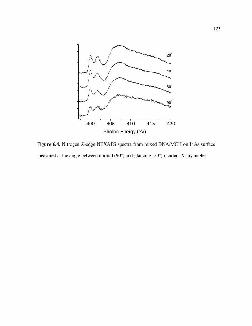
123
400 405 410 415 420
Photon Energy (eV)
20o
40o
60o
90o
Figure 6.4. Nitrogen K-edge NEXAFS spectra from mixed DNA/MCH on InAs surface
measured at the angle between normal (90°) and glancing (20°) incident X-ray angles.

124
0 30 60 900.4
0.6
0.8
1.0
Inte
nsity (
arb
. u
nits)
Polarization angle (theta)
Figure 6.5. Polarization dependence of the intensities of the π* resonance in the N K-
edge NEXAFS spectra of C1B – NaCl sample.

125
consistent with earlier NEXAFS studies of DNA absorbed on Au surface [24] and on
glass and silicon substrate [32].
6.3.4 Electronic Properties
The immobilized DNA density was effectively increased by adding 1M NaCl in
the functionalization solution as discussed previously. Comparison of the C1B sample
with the C1B-NaCl sample allows determination of the dependence of the InAs surface
electronic properties on the surface density of immobilized DNA. The binding energy is
sensitive to the interfacial electron environment and the adsorbate-induced charge
transfer associated with surface states density and the energy distribution at the interface
[33]. The BE of As-In peak in the As 3d5/2 spectrum was found at 40.73 eV for the C1B-
NaCl sample from the XPS spectra as compared to 40.69 eV for the C1B sample (Fig.
6.2.). The surface band bending of two samples is similar within the experimental error of
± 0.02 eV. We speculate that the similar surface band bending results from similar As/In
ratio on the surface of two samples as discussed previously. The ratio of As-to-In was
found to be 0.93 for the C1B-NaCl sample and 1.0 for the C1B sample (Table 6.3.). The
surface stoichiometry can determine the type and density of surface states which lead to
the pinning of the Fermi level. The work function was determined through the difference
between photon energy (He I, 21.2 eV) and the secondary electron emission edge (high
energy cutoff) of UPS spectra. The work function determined from the UPS spectra was
4.95 eV for the C1B sample and 5.10 eV for the C1B-NaCl sample as shown in Figure
6.6. The work function was increased by 0.15 eV on samples with the addition of salt to
the functionalization solution. Based on these XPS and UPS results, surface band

126
diagrams for these samples were constructed and are shown in Figure 6.7. Given the
similar interfacial band bending found on the C1B and C1B-NaCl samples, the difference
in work function may not arise from interface charge transfer. The work function is a
combination of the electron affinity and the position of the Fermi level at the surface as
well as the presence of any surface dipole layers formed across the functionalized or
absorbed layer. The changes noted here could be arise from the presence of such a
surface potential or dipole across the molecular interface. The size of the surface potential
is related to the magnitude of the molecular dipole, its direction and orientation at the
surface, and the density of molecules within this dipole layer [33]. The density of
immobilized DNA on the surface can also change the orientation of the molecular dipole.
For example, the molecule may lay parallel to the surface at a low surface coverage. The
molecule would be at a vertical angle to the surface when the molecules are densely
packed on the surface. This molecular orientation can change the surface potential
leading different measured work functions. The surface potential for the C1B and C1B-
NaCl samples was also measured using KPFM. The measured surface potentials at the
C1B and C1B-NaCl samples were 4.80 V and 4.93 V, respectively. The measured surface
potential difference was 0.13 V, which is in agreement with the value deduced from UPS
measurements with experimental error (± 0.02 eV).

127
18 15 12 9 6 3 0 18 17 16 15
Inte
nsity [
a.u
.]
BE w.r.t. EF (eV)
C1B
C1B-NaCl
(a)
Inte
nsity [
a.u
.]
BE w.r.t. EF (eV)
(b)
Figure 6.6. (a) UPS spectra and (b) secondary electron emission edge of the spectra for
the C1B and C1B-NaCl. The high energy cutoff was found at 16.25 eV for the C1B
sample and 16.10 eV for the C1B-NaCl sample.

128
Figure 6.7. Surface band diagrams at the surface. The left side of diagram is C1B, and
right side of diagram is C1B-NaCl sample.
C1B C1B-NaCl
BE(As3d5/2
) Δ BE =0.04eV
Eva
Work Function
≈
E
Δ WF =0.13eV

129
6.4 Conclusions
The effect of salt on DNA immobilization was studied by XPS, UPS and
NEXAFS measurements. The DNA functionalization was compared using two methods
(‘A’ and ‘B’ methods) with and without NaCl salt in the functionalization solution. The
NaCl-based functionalization solutions strongly increased the density of immobilized
DNA. The presence of DNA was confirmed by N 1s, P 2p, and C 1s high-resolution XPS.
When both MCH and HS-ssDNA were present in the functionalization solutions, the
interface chemistry was modified due to the preferential MCH absorption onto As atoms.
The polarization dependence of NEXAFS N K-edge spectra was used to determine the
orbital orientation. The π* orbitals of nucleobases with a random azimuthal orientation
has an average tilt of 45° away from the substrate normal. The work function associated
with surface potential increases with the increase in DNA surface density. These results
imply that the electronic properties of the InAs surfaces can be sensitively modified with
surface treatment.

130
References
[1] M. V. Lebedev, Progress in surface science 2002, 70, 153–186.
[2] D. Tsui, Physical Review Letters 1970, 24, 303–306.
[3] S. Bhargava, H.-R. Blank, V. Narayanamurti, H. Kroemer, Applied Physics Letters
1997, 70, 759.
[4] A. W. Peterson, R. J. Heaton, R. M. Georgiadis, Nucleic acids research 2001, 29,
5163–8.
[5] T. M. Herne, M. J. Tarlov, Journal of the American Chemical Society 1997, 119,
8916–8920.
[6] D. Y. Petrovykh, H. Kimura-Suda, L. J. Whitman, M. J. Tarlov, Journal of the
American Chemical Society 2003, 125, 5219–26.
[7] C. J. May, H. E. Canavan, D. G. Castner, Analytical chemistry 2004, 76, 1114–
1122.
[8] C.-Y. Lee, P. Gong, G. M. Harbers, D. W. Grainger, D. G. Castner, L. J. Gamble,
Analytical chemistry 2006, 78, 3316–25.
[9] M. Losurdo, P. C. Wu, T.-H. Kim, G. Bruno, A. S. Brown, Langmuir 2012, 28,
1235–45.
[10] E. Cho, P. Wu, M. Ahmed, A. Brown, T. F. Kuech, mater. res. soc. symp. proc.
2011, 1301, DOI 10.1557/opl.2011.75.
[11] D. Y. Petrovykh, J. C. Smith, T. D. Clark, R. Stine, L. a Baker, L. J. Whitman,
Langmuir 2009, 25, 12185–94.
[12] R. Stine, D. Y. Petrovykh, Journal of Electron Spectroscopy and Related
Phenomena 2009, 172, 42–46.
[13] D. Y. Petrovykh, M. J. Yang, L. J. Whitman, Surface Science 2003, 523, 231–240.
[14] D. Y. Petrovykh, J. M. Sullivan, L. J. Whitman, Surface and Interface Analysis
2005, 37, 989–997.

131
[15] W. Knoben, S. H. Brongersma, M. Crego-Calama, The Journal of Physical
Chemistry C 2009, 113, 18331–18340.
[16] H. Lim, C. Carraro, R. Maboudian, M. W. Pruessner, R. Ghodssi, Langmuir 2004,
20, 743–7.
[17] H. H. Park, A. Ivanisevic, The Journal of Physical Chemistry C 2007, 111, 3710–
3718.
[18] O. Dannenberger, K. Weiss, H.-J. Himmel, B. Jäger, M. Buck, C. Wöll, Thin Solid
Films 1997, 307, 183–191.
[19] Y. Zubavichus, a. Shaporenko, M. Grunze, M. Zharnikov, Nuclear Instruments
and Methods in Physics Research Section A: Accelerators, Spectrometers,
Detectors and Associated Equipment 2009, 603, 111–114.
[20] K. Kaznacheyev, A. Osanna, C. Jacobsen, V. Moruzzi, Society 2002, 3153–3168.
[21] S. E. Creager, J. Clarke, Langmuir 1994, 10, 3675–3683.
[22] M. M. Kreevoy, E. T. Harper, R. E. Duvall, H. S. Wilgus III, L. T. Ditsch, Journal
of the American Chemical Society 1960, 82, 4899–4902.
[23] C. L. McGuiness, a. Shaporenko, M. Zharnikov, a. V. Walker, D. L. Allara,
Journal of Physical Chemistry C 2007, 111, 4226–4234.
[24] D. Y. Petrovykh, V. Pérez-Dieste, A. Opdahl, H. Kimura-Suda, J. M. Sullivan, M.
J. Tarlov, F. J. Himpsel, L. J. Whitman, Journal of the American Chemical Society
2006, 128, 2–3.
[25] K. Fujii, K. Akamatsu, a. Yokoya, The Journal of Physical Chemistry B 2004, 108,
8031–8035.
[26] M. Furukawa, H. Fujisawa, S. Katano, H. Ogasawara, Y. Kim, T. Komeda, a.
Nilsson, M. Kawai, Surface Science 2003, 532-535, 261–266.
[27] K. Fujii, K. Akamatsu, Y. Muramatsu, A. Yokoya, Nuclear Instruments and
Methods in Physics Research Section B: Beam Interactions with Materials and
Atoms 2003, 199, 249–254.
[28] S. M. Kirtley, O. C. Mullins, J. Chen, J. van Elp, S. J. George, C. T. Chen, T.
O’Halloran, S. P. Cramer, Biochimica et biophysica acta 1992, 1132, 249–54.
[29] a Veareyroberts, Applied Surface Science 2004, 234, 131–137.

132
[30] J. N. Crain, a. Kirakosian, J.-L. Lin, Y. Gu, R. R. Shah, N. L. Abbott, F. J.
Himpsel, Journal of Applied Physics 2001, 90, 3291.
[31] S. M. Kirtley, O. C. Mullins, J. Chen, J. van Elp, S. J. George, C. T. Chen, T.
O’Halloran, S. P. Cramer, Biochimica et biophysica acta 1992, 1132, 249–54.
[32] J. N. Crain, a. Kirakosian, J.-L. Lin, Y. Gu, R. R. Shah, N. L. Abbott, F. J.
Himpsel, Journal of Applied Physics 2001, 90, 3291.
[33] C. A. Hacker, Solid-State Electronics 2010, 54, 1657–1664.

133
Chapter 7
Platinum Nanoclusters on Graphene grown
on SiC(0001)
This chapter was published in “Atomic-scale investigation of highly stable Pt clusters
synthesized on a graphene support for catalytic application” , by EunKyung Cho et al.,
Journal of Physical Chemistry C, v xx, n xx, p x, xx, 2012.
7.1 Introduction
Graphene exhibits a unique structure of hexagonally packed sp2-bonded carbon
atoms with single atomic thickness [1]. Graphene has been extensively studied for its
unique two-dimensional electronic structure and its extremely high mechanical and
chemical stability. Such properties make graphene an attractive supporting material for
metal particle based catalysis. Preliminary studies utilizing graphene for catalysis have
revealed the tremendous promise of graphene-based catalyst systems, but were limited to
multilayer graphene sheets and graphene-metal-oxide materials, which are not considered
ideal graphene systems [2,3]. In addition, metal adsorption on graphene is of interest in

134
the fabrication of graphene-based transistors [4,5], since metal atom adsorption can be
used to change the carrier density and tune the graphene Fermi level. For these
applications, it is critical to understand the key factors that govern the growth and
distribution of metal particles on graphene as well as the electronic and chemical
interactions of the metal atoms with graphene. Even though there is a strong motivation
to examine the metal-graphene system, the work has been limited, especially for catalysis
[4–6]. With that said, Pt nanoparticles supported on carbon materials are considered one
of the best catalysts for hydrogen oxidation and oxygen reduction in a proton-exchange
membrane fuel cell (PEMFC) [7]. Here, we have characterized the growth of platinum
nanoparticles formed on “ideal” graphene surfaces at the atomic-scale.
This chapter describes the preparation of the epitaxial graphene layers on the
silicon face of 6H-SiC(0001) and the subsequent thermal deposition of Pt atoms on these
surfaces. The evolution of the surface morphology with increasing Pt coverage and
tunneling conductance spectra are presented. These measurements are used to develop the
deposition mechanism and to study the electronic properties of the Pt clusters and their
interaction with the graphene support. A 5 min deposition of Pt resulted in a 13 %
surface coverage of Pt clusters. This sample was used in thermal annealing studies to
determine the thermal stability of the nanoparticles, which remain up to 700 °C without
any morphological changes. The surface features and cluster size were observed as a
function of thermal annealing. The Pt electronic structure, measured from the Pt clusters
before and after annealing, provides additional insight into the interaction between Pt and
the graphene substrate.

135
7.2 Experimental
The 6H-SiC(0001) single crystal samples were commercially purchased (Cree)
and degassed at 600 °C overnight in a UHV system. Both mono- and bilayer graphene
were prepared by the thermal decomposition of the SiC(0001) substrate surface through a
series of annealing steps at a temperature of 1250 °C using direct heating within the UHV
chamber. Pt atoms were thermally evaporated onto the sample at room temperature
through the e-beam heating of a Pt crucible located in the UHV chamber. After each Pt
deposition sequence, the sample was transferred and examined in situ by UHV STM and
STS at 300 K. The thermal stability of the Pt clusters on the graphene/SiC(0001) surface
was investigated by annealing. The annealing was done in situ by resistive heating in the
UHV chamber. The surface was characterized with STM and STS using an
electrochemically etched W tip. In some cases, liquid helium was used to cool the sample
to 55 K, otherwise all measurements were conducted at 300 K.
7.3 Results and Discussion
7.3.1. Deposition of Pt on Graphene
A topographic STM image of an area containing bare SiC(0001), as well as
regions of monolayer and bilayer graphene is shown in Figure 7.1(a). It is known that the
SiC(0001) surface starts to form the 30)3636( Rx reconstruction at about 1100 °C
during annealing [8], and the growth of one to three layers of graphene can be induced by

136
further heating to 1200-1350 °C. The prepared sample principally exhibits regions of
either monolayer and/or bilayer graphene on the surface. The two regions can be
distinguished via atomic resolution imaging depending on the voltage dependence and
via signatures in the scanning tunneling spectroscopy (STS) [9,10]. The first layer of
graphene was observed with higher resolution, and the characteristic hexagonal structure
is clearly seen with atomic resolution at low bias (Fig. 7.1(a), inset).
Once formation of clean graphene was confirmed by STM imaging, Pt was
deposited on the prepared graphene/SiC(0001) sample in order to study the growth
behavior of Pt nanoparticles on graphene. Figures 7.1.(b - f) display the STM images of
Pt atoms deposited onto graphene for steadily increasing deposition times of 1 min., 3
min., 5 min., 10 min., and 30 min., respectively. All of the prepared surfaces had regions
of the epitaxial graphene and the bare reconstructed SiC substrate. Initially, it is clear that
the Pt clusters are highly dispersed on the graphene surface, with a few Pt clusters
observed on the bare SiC areas. On the graphene surface, the Pt assembles into
nanoclusters indicating that the Pt atoms have sufficient mobility at room temperature to
aggregate and form the clusters. The surface coverage of Pt clusters on one layer of
graphene and on bilayer graphene appears to be similar. As expected, the Pt coverage
increases with deposition time. The cluster growth becomes a competitive process
between single atom adsorption on graphene versus attachment onto an already formed
cluster. The size distribution of Pt clusters for 5 min doses of Pt deposited on
graphene/SiC(0001) is shown in Figure 7.2. The Pt clusters are predominantly below 3
nm in diameter and 0.1 nm to 0.3 nm in height. There is a linear correlation between

137
Figure 7.1. STM images of (a) clean graphene/SiC(0001), (b) 1 min, (c) 3 min, (d) 5 min,
(e) 10 min, and (f) 30 min doses of Pt deposited on graphene/SiC(0001) at sample bias
V= –1.0 V and tunneling current I=100 pA at 300 K ((a)-(f) 100x100 nm2, scale bar in (a)
= 25 nm (a) insert 2.5 nm2).

138
Figure 7.2. Cluter height distrubution as a function of the corresponding cluster diameter
for 5 min doses of Pt deposited on graphene/SiC(0001).
0
0.1
0.2
0.3
0.4
0.5
0.6
0.0 1.0 2.0 3.0 4.0 5.0 6.0
Clu
ster
hei
gh
t [
nm
]
Cluster diameter [nm]
139
cluster diameter and height with following equation: y = 0.094 x + 0.08 (R2 = 0.75). The
Pt atoms form relatively flat clusters meaning that the Pt atoms prefer to maximize their
interactions with the C surface, instead with other Pt atoms. This may imply that the Pt-C
interactions are stronger than the Pt-Pt interactions. It should be noted that different
metals studied on graphene on SiC have exhibited different morphologies. For example,
Cobalt (Co) preferentially decorates the 30)3636( Rx reconstructed SiC surface,
rather than the monolayer graphene [6].
7.3.2. Electronic Properties of Pt/Graphene surface
Given these differing observations among metals on graphene, it is of interest to
further develop an understanding of the deposition mechanism and the interaction
between adsorbed metals and the graphene surface. Several theoretical studies [2,11,12]
have shown that Pt atoms, possessing a nearly filled d-shell, principally bind to the bridge
(B) site of the graphene surface at the midpoint of a carbon-carbon bond. Adsorption on
the B site involves hybridization between the C atom and the metal atom, and it is likely
that the graphene sp2-like orbital character partially shifts to the more covalently reactive
sp3-like character [12–14]. The schematic structure of the Pt-deposited graphene surface
is shown in Figure 7.3(a). If Pt adsorption involves the hybridization of a Pt atom and a C
atom, the electronic structure of the graphene would be significantly altered. Such
changes in the graphene electronic structure were suggested in the STM images which
exhibit a modulation of the electronic state of the graphene in the vicinity of a Pt cluster.
The modulation is almost identical to previously observed electron scattering from lattice
defects in graphene [15]. This hybridization can be used to rationalize the different

140
behaviors of Co and Pt on graphene/SiC(0001) in terms of the metal-carbon (M-C) bond
dissociation energies. It has been reported that the bond dissociation energy of Pt-C is
150 kJ/mol [16] and that of Co-C is 37 kJ/mol [17]. The stronger M-C bond would inhibit
surface diffusion at a given temperature and flux on the graphene surface [18]. The
reduced surface transport, resulting from the reduction in the diffusion coefficient, leads
to enhanced dispersion of the Pt clusters on graphene having stronger Pt-C bonds than Pt-
Pt bonds. Therefore, Pt forms small, highly dispersed clusters on graphene in contrast to
Co which forms a lower density of larger clusters.
In order to confirm the modulation of the electronic behavior of the graphene,
STS spectra were taken on the monolayer graphene and Pt clusters (points indicated in
Fig. 7.3(c)) for a graphene/SiC(0001) sample after a 5 min deposition of Pt and are
shown in Figure 7.3(d-e). Each spectrum was obtained by averaging several bias sweeps
with an initial tunneling current and bias voltage of 200 pA and 0.3 V, respectively. Fig.
3(d) shows the dI
dV spectrum taken on the monolayer graphene region away from any Pt
clusters. The spectrum is a minimum at zero bias and is similar to previously reported
STS of monolayer graphene/SiC(0001) systems [9,10]. From this similarity, we assume
that the Pt deposition did not introduce Pt atoms below the first layer of epitaxial
graphene. Figure 7.3(e) presents dI
dV curves taken and averaged on each Pt cluster as
labeled in the corresponding STM image (Fig. 7.3(c)). The peaks at the positive and
negative bias voltages are attributed to the resonant electron transfer between the STM tip
and the unoccupied and occupied electronic states of the Pt clusters, respectively. A peak

141
in the positive bias voltage range appears at 0.49 V, and this peak is common to all Pt
clusters, although the peak positions differ from cluster to cluster in the negative bias
voltage range. The various peaks have their maxima at –0.26 V, –0.37 V, or –0.66 V. The
height of the clusters named Pt1, Pt2 and Pt3 are ~ 0.23 nm and that of Pt4 is ~ 0.35 nm
with a ~ 1.5 nm width for both groups. Clusters with the same size on the surface do not
necessarily possess the same electronic structure [19]. This variation is likely to originate
from the different atomic arrangements of the clusters and the different adsorption sites
on the graphene surface below. A. Battac et al. studied deposited Pt atoms on highly-
oriented pyrolytic graphite (HOPG) and reported sharp peaks at –0.20 V and –0.40 V in
the 0 to ~ –0.5 V range of the tunneling conductance spectra [20]. They stated that the
discrete peaks in the STS spectra are due to quantum size effects. T. Kondo et al.
observed a peak in the 0 to ~ –0.08 V range in the vicinity of Pt clusters on HOPG [21].
They proposed that the peak is evidence of the nonbonding π electronic states due to the
Pt-C hybridization. Since Pt atoms have no energy levels in the range investigated [20],
the electronic structure observed in the present study could arise from either (i)
quantization of the electronic density of states due to the reduced dimensions of the
cluster [20], or (ii) states associated with the carbon atoms due to the interaction between
the Pt clusters and the graphene substrate [21].

142
Figure 7.3. (a) Schematic structure and STM topographic image of a Pt-deposited
graphene/SiC(0001) sample, (b)-(c) STM topographic images of the surface after a 5 min
deposition of Pt at sample bias V= –1.0 V and tunneling current I=200 pA, imaged at 300
K (scale bar = 5 nm in (b), 2 nm in (c), respectively), (d) STS spectrum of clean
monolayer graphene, and (e) STS spectra of various Pt clusters. The corresponding
measurement points are shown in (c).

143
7.3.3. Thermal Stability of Pt clusters on Graphene
The thermal stability of the Pt clusters on the graphene/SiC(0001) surface was
investigated by annealing the 5 min Pt-deposited sample at elevated temperatures of 400
°C, 500 °C, 600 °C, and 700 °C for one hour. The annealing was done in situ by resistive
heating in the UHV chamber. After annealing, the sample was cooled down with liquid
helium and examined by STM at 55 K with the resulting images shown in Figure 7.4. The
images are characterized by terraces of mono- and bilayer graphene decorated with the Pt
clusters. Regions of mono- and bilayer graphene are distinguished by the imaging of the
SiC surface reconstruction features. The SiC reconstruction is observed beneath single
layer graphene, but not beneath bilayer graphene when imaged at high tunneling bias as
shown in Fig. 7.4. The graphene lattice structure is superimposed on the surface
reconstruction of SiC(0001) with pyramidal clusters and hexagonal rings observed in the
STM image at low tunneling bias (Fig. 7.4(a)). These observed adatom features beneath
the first graphene layer were reported previously [9]. Interestingly, the STM images do
not show any obvious increase in the Pt cluster size over the annealing range employed
(up to 700 °C). This observation implies that there is no significant ripening or
appreciable atom detachment from the Pt clusters at high temperatures. Quantitative
analysis of Pt clusters performed on randomly selected STM images of the
graphene/SiC(0001) sample after a 5 min deposition of Pt, after annealing at 400 °C and
at 700 °C, yielded size histograms shown in Figure 7.5. The size interval of 0.2 nm was
used in the histogram. A 90% of the Pt clusters was observed in the range of 0.1 - 2.4 nm
for the as-deposited sample as well as the samples after annealing at 400 °C and at 700°C.

144
Figure 7.4. STM images of the graphene/SiC(0001) sample after a 5 min deposition of Pt
and anneal at (a) 400 °C, (b) 500 °C, (c) 600 °C, and (d) 700 °C each for one hour and
imaged at sample bias V= –0.3 V and tunneling current I=100 pA at 55 K. (Scale bar =
10 nm)

145
0.0 0.4 0.8 1.2 1.6 2.0 2.4 2.8 3.2 3.6 4.00
10
20
30
40
50N
um
ber
of
clu
ste
rs [
%]
Cluster diameter (nm)
A
0.0 0.4 0.8 1.2 1.6 2.0 2.4 2.8 3.2 3.6 4.00
5
10
15
20
25
30
Num
ber
of
clu
ste
rs [
%]
Cluster diameter (nm)
B
0.0 0.4 0.8 1.2 1.6 2.0 2.4 2.8 3.2 3.6 4.00
5
10
15
20
25
30
Num
ber
of
clu
ste
rs [
%]
Cluster diameter (nm)
C
Figure 7.5. Size distribution of the graphene/SiC(0001) sample after a 5 min deposition
of Pt (a) as-deposited, (b) after anealing at 400 °C, and (c) after annealing at 700 °C.

146
The Pt cluster size of the as-deposited sample generally shows a bimodal distribution and
two maxima at the cluster diameters of 0.1 nm and 1.5 nm. After annealing, the size
distribution of small Pt clusters (< 0.4 nm) shows some agglomeration. The median of the
Pt size distribution, the diameter separating the higher half population of the Pt clusters
from the lower half, was found at 0.20 nm before annealing, 0.49 nm after annealing at
400 °C and 700 °C. The agglomeration of Pt clusters observed on graphene is negligible
compared with the previous study on Pt supported on other carbon materials. E. Antolini
et al. have shown that Pt supported on Vulcan XC-72R carbon (VC) grew from 1 nm to
20 nm after annealing at 300 - 400 °C.[22] The absence of cluster growth or ripening is
also consistent with the strong, covalent metal-graphene bond as suggested for the
surface adsorption mechanism. Hence, these clusters are highly stable well beyond the
temperature range of several catalytic applications [23].
Additional annealing steps were carried out at 1250 °C for 30 sec, which was
repeated several times. The annealing at 1250 °C led to dramatic morphological changes
as presented in Figure 7.6. The resulting surface possesses an inhomogeneous distribution
of Pt clusters on certain terraces. The Pt clusters are only found on the bilayer graphene
and not on the monolayer graphene or the clean SiC(0001) surface. The Pt clusters on the
first layer of graphene were detached from the surface after annealing at 1250 °C. Fig. 7.6
(b) shows higher magnification topographic images of the monolayer of graphene and of
the bilayer composed of Pt/graphene after annealing at 1250 °C. No Pt clusters were
observed on the monolayer graphene, and the observed corrugation corresponds to the
underlying SiC 30)3636( Rx reconstruction. In contrast, randomly distributed clusters

147
are found on the bilayer graphene. The coverage of Pt clusters on the post-annealed
surface is ~ 8% of the overall area, which is a lower surface coverage than found on the
surface prior to annealing at 1250 °C (13% of surface coverage). The Pt clusters observed
on the post-annealed sample exhibit smooth morphology compared with the clusters
before annealing (Fig. 7.3 and Fig. 7.4). The sublimation energy of Pt is ~565 kJ/mol
[24] and the Pt-C bond dissociation energy is ~150 kJ/mol [16]. The breaking of the Pt-C
bonds is thermodynamically favored over than the sublimation of Pt. We have observed
that most of the Pt clusters on the monolayer graphene were desorbed after the annealing
procedure, implying that the annealing temperature was high enough to trigger the
breaking of Pt-C bonds and the sublimation of the Pt clusters. In addition, we have seen
Pt clusters remaining on the bilayer graphene terrace as shown in Fig. 7.6. Our
interpretation is that the Pt is intercalating in the bilayer graphene region between the two
sheets of carbon. Possible intercalation routes can be suggested by the observation of
some etch pits in the bilayer area (pointed out with arrows in Fig. 7.6(b)). This
observation indicates that the Pt is breaking bonds in the graphene leaving behind etch
pits when the sample was flashed at 1250 °C. In addition, small Pt particles seated around
the hole of the etch pits in the bilayer graphene indicate the preferential binding sites due
to presence of undercoordinated carbon atoms at edges of the pits. The breaking of the
graphene bonds indicates a sp2 sp
3 rehybridization of C on the step edge with Pt-C
bond formation. Based on these observations, we have proposed the structure of the
flashed sample schematically as shown in Fig. 7.6 (c).

148
Figure 7.6. (a-b) STM topographic images of the graphene/SiC(0001) sample after a 5
min deposition of Pt annealed at 1250 °C and imaged at sample bias V = –1.0 V,
tunneling current I = 100 pA at 300 K. (scale bar = 50 nm in (a), 25 nm in (b)), (c)
schematic structure of the Pt-deposited graphene/SiC(0001) surface after flashing
indicating the intercalation of Pt.

149
7.4 Conclusions
In summary, the morphological and electronic structure of Pt clusters formed on a
graphene/SiC(0001) substrate was determined through UHV STM and STS
measurements. The uniformly distributed, small Pt clusters were preferentially formed on
the graphene rather than on the bare reconstructed SiC(0001) surface indicating that Pt
has a stronger interaction with graphene. The electronic structure of the graphene near a
Pt cluster was modified and distinct STS peaks were observed on the Pt clusters on the
graphene surface. These STM and STS observations of both the topographical and
electronic perturbation suggested that the Pt atoms were covalently bound to the
graphene. The clusters were stable upon thermal annealing to 700 °C without significant
changes in size or distribution. The STM images of the Pt/graphene sample post-
annealing at 1250 °C indicates that the Pt may break some of the carbon bonds in
graphene and penetrate the graphene overlayer, resulting in metal intercalation in this
system. These finds suggest promising applications for graphene as catalyst supports.

150
References
[1] A. K. Geim, K. S. Novoselov, Nature materials 2007, 6, 183–91.
[2] B. F. Machado, P. Serp, Catalysis Science & Technology 2012, 2, 54.
[3] I. V. Lightcap, T. H. Kosel, P. V. Kamat, Nano letters 2010, 10, 577–83.
[4] M. Hupalo, S. Binz, M. C. Tringides, Journal of physics. Condensed matter 2011,
23, 045005.
[5] M. Hupalo, X. Liu, C.-Z. Wang, W.-C. Lu, Y.-X. Yao, K.-M. Ho, M. C. Tringides,
Advanced materials 2011, 23, 2082–7.
[6] S. W. Poon, W. Chen, E. S. Tok, A. T. S. Wee, Applied Physics Letters 2008, 92,
104102.
[7] B. Seger, P. V. Kamat, The Journal of Physical Chemistry C 2009, 113, 7990–
7995.
[8] U. Starke, C. Riedl, Journal of Physics: Condensed Matter 2009, 21, 134016.
[9] G. M. Rutter, N. P. Guisinger, J. N. Crain, E. a. a. Jarvis, M. D. Stiles, T. Li, P. N.
First, J. a. Stroscio, Physical Review B 2007, 76, 1–6.
[10] P. Lauffer, K. Emtsev, R. Graupner, T. Seyller, L. Ley, S. Reshanov, H. Weber,
Physical Review B 2008, 77, 155426.
[11] K. Nakada, a. Ishii, Solid State Communications 2011, 151, 13–16.
[12] L. Hu, X. Hu, X. Wu, C. Du, Y. Dai, J. Deng, Physica B: Condensed Matter 2010,
405, 3337–3341.
[13] P. Feibelman, Physical Review B 2009, 80, 1–4.
[14] A. T. N’Diaye, T. Gerber, C. Busse, J. Mysliveček, J. Coraux, T. Michely, New
Journal of Physics 2009, 11, 103045.
[15] G. M. Rutter, J. N. Crain, N. P. Guisinger, T. Li, P. N. First, J. A. Stroscio, Science
2007, 317, 219–22.
[16] J. Simoes, J. Beauchamp, Chemical Reviews 1990, 90, 629–688.

151
[17] B. D. Martin, R. G. Finke, J. Am. Chem. Soc. 1990, 112, 2419–2420.
[18] Z. Zhou, F. Gao, D. W. Goodman, Surface Science 2010, 604, L31–L38.
[19] H. Yasumatsu, T. Hayakawa, T. Kondow, The Journal of chemical physics 2006,
124, 14701.
[20] A. Bettac, L. Koller, V. Rank, K. Meiwes-Broer, Surface science 1998, 402, 475–
479.
[21] T. Kondo, Y. Iwasaki, Y. Honma, Y. Takagi, S. Okada, J. Nakamura, Physical
Review B 2009, 80, 2–5.
[22] E. Antolini, F. Cardellini, E. Giacometti, G. Squadrito, Journal of materials
science 2002, 37, 133–139.
[23] L. Dong, R. R. S. Gari, Z. Li, M. M. Craig, S. Hou, Carbon 2010, 48, 781–787.
[24] J. W. Arblaster, Platinum Metals Review 2005, 49, 141–149.

152
Chapter 8
Conclusions and Recommendations
8.1 Conclusions
This thesis focused on the chemical and electronic properties of InAs (100)
surfaces functionalized with single-stranded DNA probes using a variety of chemical
approaches. The principal characterization techniques were x-ray and ultraviolet
photoelectron spectroscopy (XPS and UPS) and near-edge x-ray adsorption fine structure
(NEXAFS).
Prior to DNA functionalization, various chemical procedures were used to alter
the surface chemistry and remove the native oxide from the InAs surface. The initial
chemical state of the surface resulting from the surface chemical processing was
characterized prior to functionalization. Firstly, InAs surfaces were treated with (NH4)2S
solution for sulfur passivation. The chemical and electronic studies of sulfur-passivated
InAs demonstrated that In-S bonds were formed on the surface causing changes in the
surface electronic structure. DNA functionalization on sulfur-passivated InAs and non-
passivated InAs was compared. The DNA-exposed surfaces were characterized using

153
XPS and fluorescence measurements. The DNA immobilization was observed by the
presence of fluorine and nitrogen peaks. The XPS and fluorescence measurements
indicate that the sulfur-passivated InAs surface can have a higher density of DNA
immobilized on the surface as compared to the functionalized sample without prior sulfur
passivation. However, the change in the InAs interfacial or surface chemistry upon DNA
functionalization was not clearly discerned as to whether the thiolated DNA attached onto
the sulfur present due to the prior sulfur-passivation process or had replaced the surface
bound sulfur. This result suggested that additional studies of the DNA functionalization
onto chemically prepared InAs surfaces without prior sulfur passivation were required.
To achieve direct DNA functionalization on InAs surfaces without sulfur
passivation, the effects of various chemical preparations and functionalization methods
were investigated. Before DNA functionalization, HF- and NH4OH- based aqueous
etchants and annealing procedure were used to remove the native oxide from the InAs
surface. The XPS studies of chemically-treated InAs substrates indicated that the
different cleaning methods result in different compositions of the surface oxides. Using
these chemically prepared InAs substrates, with varying compositions of surface oxides,
DNA functionalization was performed using two approaches; one used a DNA solution
containing ammonium hydroxide (‘A’ method) and the other used a Tris-EDTA (TE)
buffer-based DNA solution (‘B’ method). The interface chemistry of the functionalized
surfaces, using DNA probes which contained a thiol end group, was studied by XPS and
revealed that both As-S and In-S bonding occurred on the surface and the specific surface
or interfacial chemistry was determined by the functionalization method regardless of

154
prior chemical treatment. The ‘A’ method resulted predominantly in As-S bonding on an
As-rich surface, while the samples treated with the ‘B’ method had similar amounts of In-
S and As-S components on the treated InAs surface. The functionalization method also
affected the electronic properties of the functionalized surfaces. The CxA samples
(defined in chapter 5) showed an increased downward surface band bandings over the
CxB samples. This increased band bending was attributed to the arsenic-rich surface
and/or surface roughness, leading to different density and distribution of surface states
and surface charge, resulting from the complete chemical treatment and DNA
functionalization process. Since both thiolated DNA probes (HS-ssDNA) and
mercaptohexanol (MCH) were present in the functionalization solution, NEXAFS C K-
edge spectrum was used to determine which molecule is dominantly immobilized on the
surface. The NEXAFS study demonstrated that most of the As-S and In-S bonds on the
functionalized surfaces did not originate from the thiolated DNA probe, but rather from
the mercaptohexanol molecule. A higher DNA density is desired since the DNA density
controls the efficiency and the kinetics of the hybridization with target sequences.
The effect of NaCl in the functionalization solution on DNA immobilization was
then studied as a means to increase the immobilized DNA density. The DNA
functionalization was compared using two methods (‘A’ and ‘B’ methods) with and
without NaCl salt in the functionalization solution. The analysis of N 1s, In 3d, and As 3d
XPS core-levels found that a ten-fold increase in the density of surface-attached DNA
was achieved by the addition of salt within the DNA functionalization solution compared
with the samples prepared without salt. When both MCH and HS-ssDNA were present in

155
the functionalization solutions, the interface chemistry was characterized by the
preferential MCH absorption onto As atoms with a high pH functionalization solution.
The InAs work function increased with an increased immobilized DNA density while the
surface band bending was not affected by the DNA density on the surface. This change in
work function was attributed to the change in surface potential caused by differing DNA
molecular orientation which was dependent on the DNA coverage. These results imply
that the electronic properties of the InAs surfaces can be sensitively modified with
surface treatment. In addition, the polarization dependence of NEXAFS N K-edge spectra
was used to determine the DNA orbital orientation. The π* orbitals of nucleobases with a
random azimuthal orientation have an average tilt of 45° away from the substrate normal.
The results of this study provide a fundamental understanding of surface
chemistry and electronic properties as a function of surface treatment. The interfacial
chemistry as well as electronic properties show drastically different behavior in response
to the functionalization condition regardless of the prior cleaning procedure. This result
shows that the influence of functionalization procedure must be taken into account when
designing potential DNA biosensors devices. This work also demonstrates that the
density of DNA probe can be significantly altered by introducing NaCl into the
functionalization solution. This result may suggest that the DNA density can be
sensitively modified with functionalization chemistry. The electronic properties of the
functionalized surfaces are modified by the DNA surface coverage as well as specific
functionalization chemistry. This result suggests that there is promise in electronically
detecting the molecular adsorption on InAs substrate and DNA binding events in

156
particular. Overall, the study on the chemical and electronic structure of functionalized
InAs surfaces provides insight into how the chemical and electronic properties of the
InAs surfaces sensitively modulated by surface chemical processing and with the DNA
immobilization.
In the latter part of the thesis, the morphological and electronic structure of
platinum deposited on graphene was investigated using scanning tunneling microscopy
and spectroscopy (STM and STS) as an ancillary study. The study demonstrates that the
Pt nanoclusters can be uniformly deposited on both mono- and bilayer graphene rather
than on the bare SiC surface. The deposited Pt atoms were covalently bound to graphene
surface based on the observation of electronic scattering and high thermal stability. The
study on thermal stability of the deposited Pt atoms shows that the Pt clusters were stable
on the surface and did not by agglomerate or suffer atom detachment. The finding of this
study suggested the utilization of graphene as a support for nanoparticle catalysts.

157
8.2 Recommendations for Future Work
The field of InAs-based biosensors, or III-V semiconductor-based biosensor in
general, is still in its infancy and there are many fundamental aspects to be understood
with regards to the surface chemistry and electronic properties of the surface upon
functionalization. With this understanding, the surfaces can be engineered with a desired
molecule and the well-defined interface can be used as a biosensor platform. In addition,
the electrical signal from the functionalized substrate should be understood through
correlation of the chemical and electronic properties of the functionalized surfaces. Some
suggestions for future work are:
The work described in this thesis is focused on DNA functionalization of InAs.
Understanding the hybridization process with the target sequence is required to
employ the functionalized surface as a biosensor platform. It would be useful to
now study the effect of the hybridization process at different DNA density on the
surface electronic properties of the InAs. The immobilization density can be
determined by controlling the exposure time of the substrate to the
functionalization solution [1]. The performance of the DNA biosensor is strongly
dependent upon the hybridization efficiency. The hybridization efficiency on gold
may behave in an analogous way, suggesting that the hybridization efficiency and
the kinetics of target capture are a function of DNA immobilization density [2].
A complete set of electrical measurements upon DNA immobilization and
hybridization with target sequences would show the sensitivity and specificity of
InAs-based DNA biosensors. For sensing applications, the functionalization and

158
hybridization events must be converted into a useable electronic signal. Since the
InAs-based sensor utilizes the InAs surface electron gas, which is modified upon
molecular absorption, the modulation can have a direct impact on carrier density
and mobility of the substrate. Therefore the sensitivity of the DNA biosensor can
be monitored by a Hall measurement or other suitable measurement of the surface
conductivity or mobility. Additionally, a high specificity of the DNA biosensor is
clearly desired for the diagnosis of disease. Despite the stringently controlled
hybridization efficiency, most DNA biosensors are not capable of selectively
distinguishing single-base mismatches [3]. The specificity of the biosensor can be
determined by using target sequences that have one or more base mismatches. In
this way, the sensitivity and specificity of the InAs-based biosensor could be
determined. Some work in this area has already been completed in collaboration
with the group of Professor April Brown at Duke University.
The use of graphene as a catalytic support for platinum nanoclusters has been
studied in this thesis. Even though the morphology and electronic structures as well as
thermal stability have been studied, the catalytic activity using the Pt/graphene system
has not been investigated. It would be useful to investigate the electrocatalytic activity of
the Pt/graphene system, such as by cyclic voltammetry. In addition, other catalytic metals,
such as Au, Pd, Ag, Re, Ir and etc., could be studied to produce other metal-graphene
systems to show the potential of graphene as a catalytic support. Depending on the metal,
the dispersion and morphology of the metal on the graphene surface would be different

159
[4]. Furthermore, the metal-decorated graphene surface is attractive not only in catalytic
applications, but also in many other applications such as hydrogen storage [5] and sensors
[6,7]. Therefore fundamental studies of metal dispersed on graphene could have
widespread technological impact.
160
REFERENCES
[1] A. B. Steel, T. M. Herne, M. J. Tarlov, Analytical Chemistry 1998, 70, 4670–7.
[2] A. W. Peterson, R. J. Heaton, R. M. Georgiadis, Nucleic Acids Research 2001, 29,
5163–8.
[3] J. Wang, E. Palecek, P. Nielsen, G. Rivas, X. Cai, H. Shiraish, Na. Dontha, D. Luo,
F. Percio A.M., Journal of the American Chemical Society 1996, 118, 7667–7670.
[4] B. F. Machado, P. Serp, Catalysis Science & Technology 2012, 2, 54.
[5] H. Lee, J. Ihm, M. L. Cohen, S. G. Louie, Nano Letters 2010, 10, 793–8.
[6] A. Kaniyoor, R. Imran Jafri, T. Arockiadoss, S. Ramaprabhu, Nanoscale 2009, 1,
382–6.
[7] T. T. Baby, S. S. J. Aravind, T. Arockiadoss, R. B. Rakhi, S. Ramaprabhu, Sensors
and Actuators B: Chemical 2010, 145, 71–77.