Embed Size (px)
Citation preview
342 Chem. Soc. Rev., 2013, 42, 342--365 This journal is c The Royal Society of Chemistry 2013
Cite this: Chem. Soc. Rev.,2013, 42, 342
Scalable synthesis and device integration ofself-registered one-dimensional zinc oxidenanostructures and related materials
Babak Nikoobakht,*a Xudong Wang,*b Andrew Herzinga and Jian Shib
On integrating one-dimensional (1D) nanocrystals (nanowires) to useful devices, in this review article, we
provide a background on vapor-based growth processes and how they impact device integration strategies.
Successful integration of nanowires to devices and their scalability simply rely on where and how nanowires
are formed, how they are interfaced to other device components and how they function. In this direction,
we will provide a discussion on developed growth strategies for lateral and standing growth of
semiconductor nanostructures and assess their success in addressing current challenges of nanotechnology
such as mass integration of nanowires, and the necessary accuracy in their positioning and alignment. In
this regard, we highlight some of our recent work on formation of two-dimensional (2D)- and three-
dimensional (3D)- nanowire and nanowall arrays and provide an overview of their structural and electro-
optical properties. This will be followed by discussing potential applications of such hierarchical assemblies
in light generation, photocatalysis and conversion of motion to electricity.
1. Introduction
Optical lithography continues to be the most prevalent technique forfurther miniaturization of electronic circuitry and its components.However, as device miniaturization continues, both complexityof pattern generation and its cost increase,1 limiting the use ofsuch techniques to high-end applications, such as micro-processor manufacturing. As an alternative, nanomaterials and
a Surface and Microanalysis Science Division, 100 Bureau Dr Stop 8372, National
Institute of Standards and Technology, Gaithersburg, MD, USA 20899.
E-mail: [email protected]; Fax: +1 30 1926 6689; Tel: +1 30 19753230b Materials Science and Engineering Department, University of Wisconsin-Madison,
Madison, WI, USA 53706. E-mail: [email protected]; Fax: +1 608 262 8353;
Tel: +1 608 890 2667
Babak Nikoobakht
Babak Nikoobakht is a physicalchemist at the MaterialMeasurement Laboratory of theNational Institute of Standardsand Technology in Gaithersburg,MD. He also holds an adjunctfaculty position at the chemistryand biochemistry department ofUniversity of Maryland-CollegePark. He received his PhD fromGeorgia Institute of Technologyin 2002. His research interestsinclude anisotropic growth ofnanocrystals and exploring
relation between structure, property and function of ensemble ofone-dimensional nanocrystals.
Xudong Wang
Dr Xudong Wang is an assistantprofessor in the department ofMaterials Science and Engineeringat University of Wisconsin –Madison. He received his PhDdegree from Georgia Tech in 2005.His current research interestsinclude studying the growth andassembly of oxide nanostructuresfor mechanical and solar energyharvesting, and understanding thecoupling effect of semiconductorproperties and piezoelectricpolarization.
Received 30th April 2012
DOI: 10.1039/c2cs35164a
www.rsc.org/csr
Chem Soc Rev
REVIEW ARTICLE
Dow
nloa
ded
on 1
0 D
ecem
ber
2012
Publ
ishe
d on
28
Sept
embe
r 20
12 o
n ht
tp://
pubs
.rsc
.org
| do
i:10.
1039
/C2C
S351
64A
View Article OnlineView Journal | View Issue
This journal is c The Royal Society of Chemistry 2013 Chem. Soc. Rev., 2013, 42, 342--365 343
non-conventional nanofabrication methods such as ‘‘bottom-up’’chemical approaches could offer platforms to fill the technologicalgaps with potential advantages in terms of performance and/or cost.
Foreseen for many applications, the expected function of ananostructure in a given device is not the only specification onthe quality assurance check list. There are other requirementsincluding structural and performance reliabilities that must beunderstood and modeled in order for the nanodevice to beconsidered industrially and commercially viable. In this regard,mass interfacing of semiconductor nanostructures with othersemiconductors or metals remains among the technical barriersthat must be addressed for realization of platforms that enablecontrol over circuit topology and devices therein. Furthermore,chemical, physical and structural properties of these junctionsas well as the device functions must be predictable.
In this review article, we provide readers an account on theprogress, challenges and underlying problems in developing use-ful architectures for nanodevice fabrication via vapor depositiontechniques. This overview also provides examples on popularsemiconductor oxides such as ZnO and TiO2 and discussesimportant elements needed in the process of materials design todevice innovation, though, the underlying emphasis remains onthe directed assembly and interfacing of 1D-nanostructures. Thisis an important topic, which has to be addressed in any nanowiredevice integration regardless of the nanowire growth method. Theevaluation of candidate materials, their applications and thecritical issues related to producing practical devices, both in planarand free-standing formats will be discussed as well.
2. Significance of 1D-semiconductors andthe need for alignment techniques
1D-nanostructures share some common characteristics withtheir 0D- and 2D- counterparts, such as quantum size effects,but geometrically offer advantages that are absent or difficult to
realize using the other two categories.2 By definition, nanowiresoffer a unique combination of dimensionality, where thelongitudinal direction exceeds hundreds of nanometers or evenmicrometers in length while the transverse direction is con-fined to a few tens of nanometers or less. Since the former isaccessible using current microfabrication techniques, the topo-graphies and architectures of nanowire-based devices offer thepotential for probing materials at the sub-100 nm dimension.
In addition, due to their larger surface area, they are moresusceptible in sensing the variation in their immediate sur-roundings. This has led to realization of novel platforms, forinstance, in biosensing.3 2D-film growth typically requirescumbersome growth chambers while high quality nanowirescan be formed using inexpensive vapor phase transport orsolution-based methods. As discussed in the following sections,nanowires offer the ability to form unconventional crystals, e.g.,by extending their anisotropic growth to a 3D network such ashyperbranched nanowires. Using such nanosystems, it is alsopossible to realize crystal facets that are not thermodynamicallyobservable in thin films; for instance, the formation of non-polar facets in wurtzite crystals important in light emittingdevices. Other benefits exhibited by nanowires, compared to a2D film, could include more degrees of freedom in managingtheir defects, lattice constant, lattice strain, and doping profile.Owing to their small volume and interfacial areas, the aboveproperties are expected to result in novel material combina-tions and device concepts.
Some of the earliest reports on the growth of nanowires orwhiskers dates back to the 1960s4,5 and 1970s.6–8 However,research on 1D-nanostructures was limited until the late 1990sboom of research on this topic,9–11 perhaps due to the rise indemand for alternative nanosystems to silicon microelectronics.Nowadays, research on nanowires has deeply penetrated variousdisciplines including chemistry, materials science, physics, biologyand engineering with emerging applications in clean energy,sensors, catalysis, electronics and digital displays.
Andrew Herzing
Andrew Herzing received his PhDin Materials Science from LehighUniversity in 2007 under thesupervision of Prof. ChristopherKiely. He was subsequentlyawarded a National ResearchCouncil postdoctoral fellowshipto study the nano- and atomic-scale characterization ofmaterials using transmissionelectron microscopy andmicroanalysis techniques at theNational Institute of Standardsand Technology (NIST) in
Gaithersburg, MD. Currently a staff scientist in NIST’s MaterialMeasurement Laboratory, he is developing techniques to enablethe structural and chemical analysis of nanomaterials at ultrahighspatial resolution.
Jian Shi
Jian Shi obtained his BS degreein Materials Science andEngineering at Xi’an JiaotongUniversity in 2006, MS Degree inMechanical Engineering at theUniversity of Missouri-Columbiain 2008, and is currentlyfinishing his PhD degree underthe supervision of Prof. XudongWang in Materials ScienceProgram at the University ofWisconsin-Madison. Hisresearch focuses on thenucleation and growth of oxide
nanomaterials, photovoltaics, photoelectrochemical cells,nanogenerators and piezotronics.
Review Article Chem Soc Rev
Dow
nloa
ded
on 1
0 D
ecem
ber
2012
Publ
ishe
d on
28
Sept
embe
r 20
12 o
n ht
tp://
pubs
.rsc
.org
| do
i:10.
1039
/C2C
S351
64A
View Article Online
344 Chem. Soc. Rev., 2013, 42, 342--365 This journal is c The Royal Society of Chemistry 2013
One of the fundamental challenges in integrating free-standingsemiconductor nanowires with the highly ordered components ofan electro-optical or electro-mechanical device is being able tocontrol the overall hierarchy of nanowires either in planar orstanding format.12–14 Another issue is how to accurately positionthe active area of the individual nanowires between the necessaryelectrodes within a device. An ideal method for controlling theseparameters should enable the reproducible placement of nanowireson a large scale such that their position and orientation arepredictable. In recent years, several methods have been devisedfor incorporating free-standing nanowires into planar devices. Thecommon feature in these methods is the need for a substrateto receive the nanowires and an external force to drive the transferand alignment of nanowires onto this substrate. A variety ofdriving forces such as capillary forces,15,16 shear stress,17 adhesionforces,18–20 inertial forces21 and nanopatterning18,22 have beenutilized to control the orientation of an ensemble of nanowires ona given surface. Among them, nanoimprint lithography and patterntransfer techniques23,24 demonstrate the most promise in terms ofprecision and control. However, their use becomes challenging andcostly as the relevant object sizes drop below 100 nm or asnanoobject number per site is reduced. Overall, current techno-logies are more suited to the collective integration of monolayersof nanowires with devices; for instance, in flexible electronics,25
transistors,13 and sensory applications.12 For applications thatrequire electrically addressing single or small groups of nanowiresin a scalable fashion, the inherent uncertainties of the availabletechniques make them incapable of competing with top-downstrategies for the realization of complex architectures and circuitries.
3. Growth mechanisms of nanowires andchallenges in scalable interfacing
In general the synthesis of nanowires can be classified into twogroups of growth processes: metal-catalyzed, and metal-free7 thatcan take place in solution and in the gas phase. In the first group,also known as vapour–liquid–solid (VLS), vapor–solid–solid (VSS)and solution–liquid–solid (SLS) growth techniques, a metal catalystacting as a nanoscale solution, dissolves the incoming semi-conductor precursors from the gaseous (or solution) phase andconfines the nanocrystal growth, resulting in the formation of free-standing nanowires. Such nanowires can typically be distinguishedfrom those produced via other growth processes by the observationof a solidified droplet at their tip. In contrast, metal-free nanowiregrowth is generally considered to be a vapor–solid (VS) or solution–solid (SS) growth process. Among the factors that are known toinitiate this type of growth are surface defects in the substrate suchas impurities or screw-type dislocations.7,26 In addition, imbal-ances in the stoichiometric ratio of the precursors during crystalgrowth could also result in precipitation of an excess componenton some crystal facets, thus stimulating the VS or SS growth.27 Insolution phase, nanowires are generally grown in colloidalform28,29 or on a solid surface.30,31 In this case, analogues to theVS growth, nucleation sites are typically necessary to initiate thegrowth. Examples include growth of ZnO or TiO2 nanowires in
which a seed layer is first deposited on the surface of interest tostart the growth. Similar to gas phase techniques, this method isalso shown to be capable of forming well-aligned and high qualityfree-standing nanowires32–34 with applications in hydrogen gen-eration,35 dye-sensitized solar cells,36 and energy generation.37
Site selectivity of the growth in both gas phase and solutionphase methods have been controlled using natural surface defectssuch as screw dislocations of the underlying substrate26 or usingsurface patterning techniques. Although the first approach isinherently scalable, its main drawback is the lack of site specifi-city. The surface patterning can predictably control the position ofthe nanowires and has been shown on small scales via highresolution patterning,38 and on larger scales using interferencephotolithography.39 Masking a surface with 1D nanopatterns hasalso been used for horizontal growth of nanowires in which theyare either grown nearly parallel to the surface, but in a suspendedform,37 or grown laterally in full-contact with the substrate.22 Inthe latter group of approaches, the width of the opening in themask determines the nanowire width. As such, to grow smalldiameter nanostructures, it becomes necessary to use high resolu-tion lithography for nanopattern generation.22
ZnO and TiO2 are the two most intensively studied semi-conductor oxide materials and many of their methods of synthesishave been successfully applied for 1D-growth of other nanostructuressuch as SnO2 (catalytic VLS, Molecular Beam Epitaxy, Pulsed LaserDeposition),40–43 V2O5 (thermal evaporation, hydrothermal, sol–geland electrodeposition),44–47 WO3 (CVD, hydrothermal, electro-deposition),48–50 and Fe2O3 (CVD, flame synthesis).51–53 As it canbe seen, nanowire growth strategies including VLS, SLS, VS or SSare well-developed and offer unique capabilities such as simpli-city, scalability, site specificity, control over composition andcontrol over morphology. These methods can be utilized sepa-rately or combined to prepare nanostructures with unprece-dented form factors such as homo- and heterojunctions,tubular quantum wells, and shells with axial or radial config-urations.54–62 Diversity in device shape is one of the uniquedistinctions of 1D-nanocrystals that cannot be achieved in2D-films due to geometrical constrains.
In interfacing nanowires, it is the nature of an application or adevice function that determines the method of integration andthe necessary hierarchy of nanowires in a device. For instance, if a2D-network of nanowires is needed to form an electrically con-ductive layer, then control over the registration of the nanowiresmay not be as important as their electrical connectivity within thenetwork. However, if the application requires charge transportthrough a single nanowire or a particular group of nanowires,without intercepting each other, then control over their relativeposition and orientation becomes crucial. One of the existingchallenges is that most of the methods highlighted above yieldrandomly distributed nanowire networks which their interfacingto outside world is a daunting task. One quick fix to this limitationhas been the use of bulk of nanowires in randomly distributednanowire networks, however, this arrangement typically do notexhibit the performance of original nanowires.
In addition to the use of alignment techniques discussed inSection 2 for building 2D- or 3D-nanoarchitectures, intrinsic
Chem Soc Rev Review Article
Dow
nloa
ded
on 1
0 D
ecem
ber
2012
Publ
ishe
d on
28
Sept
embe
r 20
12 o
n ht
tp://
pubs
.rsc
.org
| do
i:10.
1039
/C2C
S351
64A
View Article Online
This journal is c The Royal Society of Chemistry 2013 Chem. Soc. Rev., 2013, 42, 342--365 345
structural relationship between a substrate and nanowires canbe used to control their overall hierarchy. These approachesnaturally enable control of the organization of nanostructureson a wafer scale, leading to more facile device integration. Oneof the requirements of this methodology is the ability topredictably guide the growth of 1D-nanostructure from a specificsite and facet. In the following sections the focus is given to themutual interactions between substrate and nanowires and factorsthat guide the nanocrystal growth on or from a single crystalsubstrate. Well known examples of these processes are free-standing and lateral growth of semiconductor nanowires, whichare discussed in the following sections.
3.1 In-plane and out-of plane directed growth of nanowires
The anisotropy of a crystal, in general, is a result of the varyinggrowth kinetics of different crystal faces. One of the fundamentalneeds in anisotropic crystal growth is the development of methodsto selectively grow a nanocrystal facet in a certain direction. Free-standing nanowires are great examples of this as growth occursonly along a selective facet, and thus in a specific crystallographicdirection. The particular direction in which a given nanowire willgrow is strongly influenced by the crystal structure of the nanowireitself, as well as by the surface free-energy of the metal andsemiconductor interface. For example, nanowires with cubicstructures typically grow in the h111i direction, while those withwurtzite-type crystal structure tend to grow in the h001i direction.63
The substrate is also considered one of the factors determining thegrowth direction of free-standing nanowires. In the case of latticematched epitaxies, they can be chosen to guide the growth in adirection which is either normal to or inclined with respect to thesurface; for instance, the growth of Si nanowires on a Si (001)substrate, which takes place in the h111i direction.11 Even in latticemismatched systems, it has been shown that the substrate impactsthe growth direction of the nanowires. Examples include thepreference for epitaxial and upright growth of InAs and InPnanowires to occur in the h111i directions on a Si (111) surface.As the diameter of such nanowires increases, population of thetilted nanowires increases, most likely to reduce the misfitstrain between the two crystals.64 In these examples, the growthis no longer epitaxial above a critical diameter due to theincrease in strain energy at the interface and the formation ofmisfit dislocations.65
In addition to the role played by the substrate, the interfacialenergy and surface tension from the edge of the interface betweenthe metal catalyst and a nanowire are found to be importantfactors in determining the growth direction of nanowires. In thecase of Si nanowires, as the diameter increases the plane of growthchanges in order to lower the interface energies between metalcatalyst and the semiconductor.66,67 For instance, the growthdirection of a population of nanowires has been shown to changefrom the h111i to the h110i direction as their diameter increasesabove 20 nm.68 Other factors affecting the diversity in nanowiregrowth directions include the growth temperature, concentrationof precursors in the gas phase11 and degree of the supersaturationinside the metal catalyst.63 Although the origin of the multiplicityof nanowire growth direction is fairly well understood, factors that
can selectively initiate or abort growth of a specific facet remainelusive. In this regard, we will discuss how the inherent informa-tion present on the surface of a single crystal substrate has beenutilized as a scaffold to promote growth of 1D- and 2D-epilayers ofother materials. This is followed by a discussion on weaknessesand strengths of available approaches in planar growth of nano-wires with higher precision and predictability.
Reports on the planar or lateral growth of 1D-nanostructureshave been very limited relative to those focused on free standingnanowires. The planar growth can be linked to the original workon the self-assembled epitaxial growth of quantum dots, whereepitaxially grown films undergo a transformation to arrays of 3Dislands.69 The island formation is typically accompanied bygeneration of misfit dislocations depending on the extent of latticemismatch. In the case of Ge on Si (E4% lattice mismatch),Eaglesham and Cerullo discovered dislocation-free island for-mation at the expense of elastic deformation of the surroundingsubstrate. As the islands are overgrown above a critical thickness,misfit dislocations appear as a stress-relief mechanism.70 If thestress is anisotropic, as in the case of Ge on Si, the island alignsitself perpendicularly to the direction of maximum stress. As thelattice mismatch increases, the anisotropy in the island shapebecomes more pronounced. Anisotropy in crystal lattice match ona cubic substrate, such as silicon, has been used to transform thinfilms of rare earth silicides into metal silicide nanowires under athermal annealing process. As a result of this heat treatment metalsilicide nanowires are formed that are approximately 1 mm inlength and 2 nm in height.71 Such growth methods typicallyrequire dissociation and reconstruction of surface deposited atomson the heated silicon surface in order to drive the formationof nanowires or quantum wires. In these cases, as the latticemismatch along the width of the nanowires increases, both thewidth and height of the nanowires tends to decrease.72 The widthdistribution of such nanowires is very broad indicating that theirformation takes place far from equilibrium. In most of these cases,nanowires tend to grow from both ends and nucleate in closely-spaced groups, with no control over their location or orientation.
Lateral growth of nanowires is also shown to be driven byanisotropy in surface energy73 and symmetry breakdown of theunderlying substrate.74 In the latter approach, also called ‘‘endo-taxial’’ growth, transition metals are deposited on a Si surface atelevated temperatures. The epitaxial growth of nanowires con-tinues into the substrate such that two of their long facets becomeembedded in the underlying silicon. The anisotropy driving thenanowire shape has been attributed to the varying growth rates ofthe nanowire end facets versus its embedded side facets. Thissynthetic route is applicable to a variety of transition metals, butlacks the necessary control of the overall nanowire morphology.Lower temperatures have been used to increase the aspect ratio ofthe resulting nanowires, but this also increases the nucleationsites, i.e., their surface density, which decreases their spacing.75
Self-organization of 1D-nanostructures has been also shownusing surface defects or structures on a single crystal surface.These approaches can be considered part of the graphoepitaxymethodologies (a.k.a artificial epitaxy) in which artificial micro-patterns on a surface are used for growth of oriented crystals.
Review Article Chem Soc Rev
Dow
nloa
ded
on 1
0 D
ecem
ber
2012
Publ
ishe
d on
28
Sept
embe
r 20
12 o
n ht
tp://
pubs
.rsc
.org
| do
i:10.
1039
/C2C
S351
64A
View Article Online
346 Chem. Soc. Rev., 2013, 42, 342--365 This journal is c The Royal Society of Chemistry 2013
Developed in the early 1970s, this approach was originallyproposed for epitaxial thin film growth on amorphous surfaces.76
The created surface patterns must have a symmetry analogous tothat of the material to be crystallized on the surface.76 Foranisotropic nanostructure growth, single crystal surfaces deco-rated with surface reconstructions or atomic steps have been usedin order to control the directionality or alignment of the grown1D-nanostructures. Examples include the use of arrays of Al atomof a-plane sapphire,77 atomic steps78 for the alignment of single-walled carbon nanotubes, or the growth of Ge nanowires on stepdefects on a silicon (113) substrate.79 These approaches offer low-level control of orientation of the resulting nanowires in theformed hierarchy. However, they do not allow for any control overthe reproducibility of the surface nanopatterns. The use ofarrangement of atoms on a crystal surface potentially is one ofthe ultimate mechanisms to precisely guide 1D-planar growth;however, the homogeneity of substrate surface energy causes theovergrown islands to lack site-specificity and thus grow randomly.To break this surface degeneracy, metal nanodroplets used in theVLS growth process are found to be very unique, as they preciselydefine the nucleation sites and confine the nanocrystals growth.
3.2 Surface-directed growth of nanowires
The surface-directed vapour–liquid–solid (SVLS) growth process isnearly identical to the VLS growth of standing nanowires. In thelatter, a metal nanodroplet as a solution captures the incomingprecursors from the gas phase, reaches a state of supersaturation,and allows precipitation of a semiconductor nanocrystal on thesubstrate. The metal nanodroplet positioned atop the formedresulting nanocrystal gradually grows upward.5,7 In the SVLSprocess, the metal nanodroplet partially wets the semiconductornanocrystal and also forms an interface with the substrate.Continuation of this process results in the lateral growth of asemiconductor nanocrystal in a specific direction with the metalnanodroplet at the leading end of the nanowire.80,81
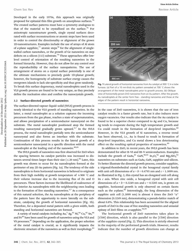
The SVLS growth of nanowires was first observed for ZnO whenthe spacing between Au catalyst particles was increased to dis-tances several times larger than their size (r20 nm).82 Later, thisgrowth was shown to occur for Au nanodroplets formed at theperimeter of any 2D Au pattern (Fig. 1a). The tendency of the sidenanodroplets to form horizontal nanowires is believed to originatefrom their high mobility at growth temperature of E900 1C andtheir volume increase due to the incoming flux of Zn and Oprecursors. These factors increase the likelihood of coalescence ofthe interior Au nanodroplets with the neighbouring ones leadingto the formation of free standing nanowires.3,7 As a consequenceof this natural selection, the Au nanodroplets at the periphery ofthe pattern have the opportunity to move laterally on the sub-strate, catalysing the growth of horizontal nanowires (Fig. 1b).Therefore, for a deposited metal pattern with a given width, bothstanding and horizontal nanowires are formed.
A variety of metal catalysts including Au,5 Ag,83 Ni,84 Cu,85 Sn,86
and Fe84 have been used for growth of nanowires using the VLS andVS processes.87 Depending on the application, the proper selectionof the metal catalyst is crucial, as it significantly impacts theelectronic structure of the nanowires as well as their morphology.83
In the case of ZnO nanowires, it is shown that the use of ironcatalyst results in a faster growth rate, but it also induces moreoxygen vacancies. Our results also indicate that the Au catalyst isfound to be a superior choice compared to Ag and Cu, becauseAg tends to evaporate during the high temperature growth andCu could result in the formation of deep-level impurities.88
However, in the VLS growth of Si nanowires, a reverse trendhas been observed, i.e., Au is found to result in formation ofdeep-level impurities, and Cu metal shows a less deterioratingeffect on the resulting optical properties of nanowires.89
In addition to ZnO, in recent years, the SVLS growth has beendemonstrated for other II–VI and III–V semiconductors. Examplesinclude the growth of GaAs,81 GaN,90,91 In2O3
92 and Mg2SiO493
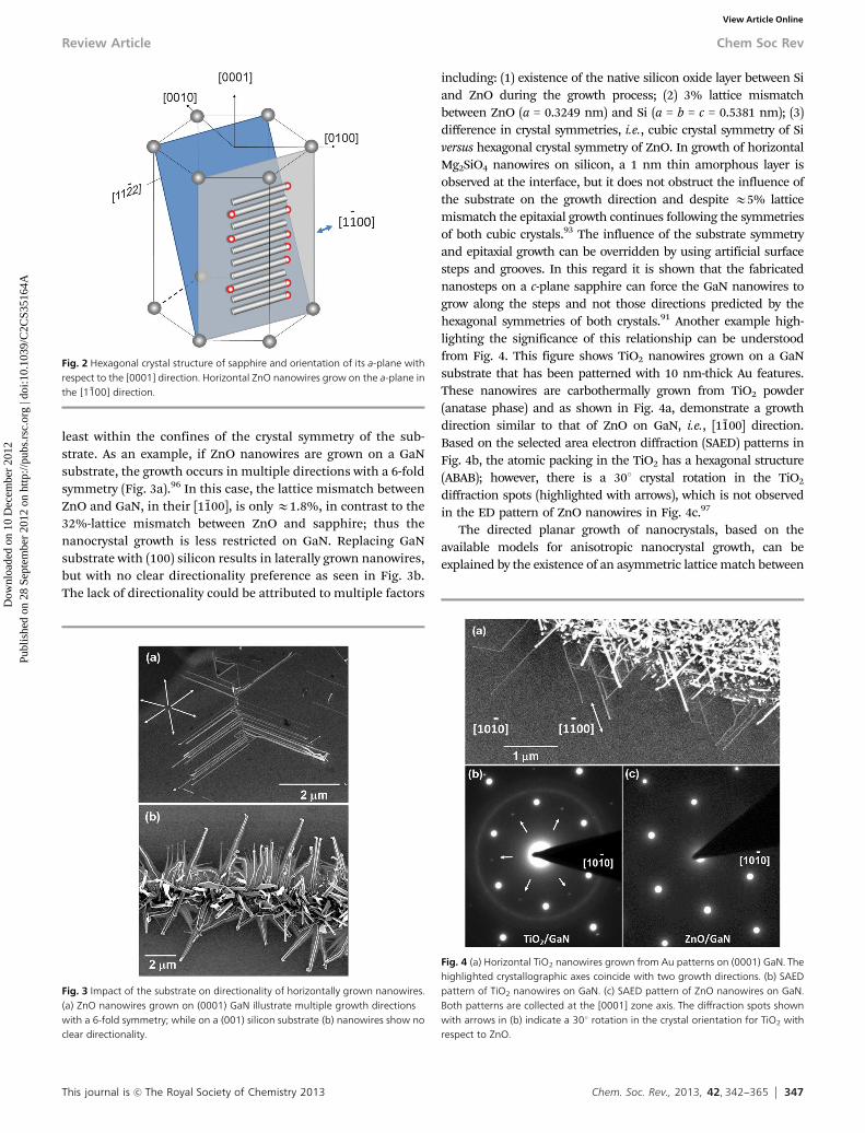
nanowires on substrates such as GaAs, GaN, sapphire and silicon.To better illustrate the directed growth process, consider sapphire,a trigonal/rhombohedral crystal in the hexagonal crystal familywith unit cell dimensions of a = b = 0.4795 nm and c = 1.3099 nm.As illustrated in Fig. 2, this crystal has an elongated unit cell alongits c axis. When zinc oxide, a hexagonal crystal with unit celldimensions of a = b = 0.3249 nm and c = 0.5205 nm, is grown onsapphire, horizontal growth is only observed on certain facetssuch as the a-plane.82 Interestingly, the long dimension of thesapphire unit cell (1.3099 nm) is almost 4 times the ZnO ‘‘a’’dimension (0.3249 nm), demonstrating a pseudo-lattice match ofabout 0.8%. This relationship has been accounted for the alignedgrowth of ZnO in the case of free standing nanowires and uniaxialepitaxy of ZnO films on a-sapphire.94,95
The horizontal growth of ZnO nanowires takes place in[1%100] direction, which is also parallel to the [1%100] directionof the sapphire crystal (Fig. 2). This direction is strictly observedin the majority of the performed growth trials. However, resultsindicate that the number of growth directions can change at
Fig. 1 Lateral growth of horizontal nanowires from Au catalyst at 900 1C in a tubefurnace. (a) Part of a 10 nm-thick Au pattern annealed at 700 1C shows thearrangement of the metal nanodroplets prior to growth process. (b) Obliqueview of horizontally grown ZnO nanowires from an Au pattern. After the growth,Au nanodroplets at the center form free – standing nanowires and those at theedges of the pattern result in horizontal nanowires.
Chem Soc Rev Review Article
Dow
nloa
ded
on 1
0 D
ecem
ber
2012
Publ
ishe
d on
28
Sept
embe
r 20
12 o
n ht
tp://
pubs
.rsc
.org
| do
i:10.
1039
/C2C
S351
64A
View Article Online
This journal is c The Royal Society of Chemistry 2013 Chem. Soc. Rev., 2013, 42, 342--365 347
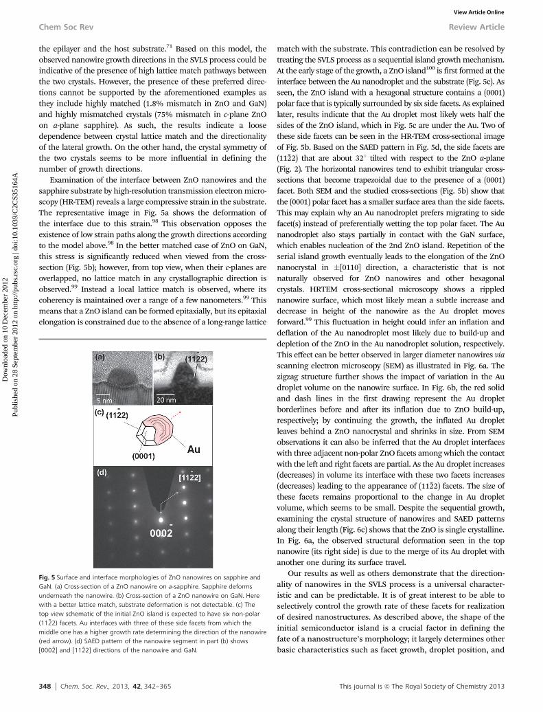
least within the confines of the crystal symmetry of the sub-strate. As an example, if ZnO nanowires are grown on a GaNsubstrate, the growth occurs in multiple directions with a 6-foldsymmetry (Fig. 3a).96 In this case, the lattice mismatch betweenZnO and GaN, in their [1%100], is only E1.8%, in contrast to the32%-lattice mismatch between ZnO and sapphire; thus thenanocrystal growth is less restricted on GaN. Replacing GaNsubstrate with (100) silicon results in laterally grown nanowires,but with no clear directionality preference as seen in Fig. 3b.The lack of directionality could be attributed to multiple factors
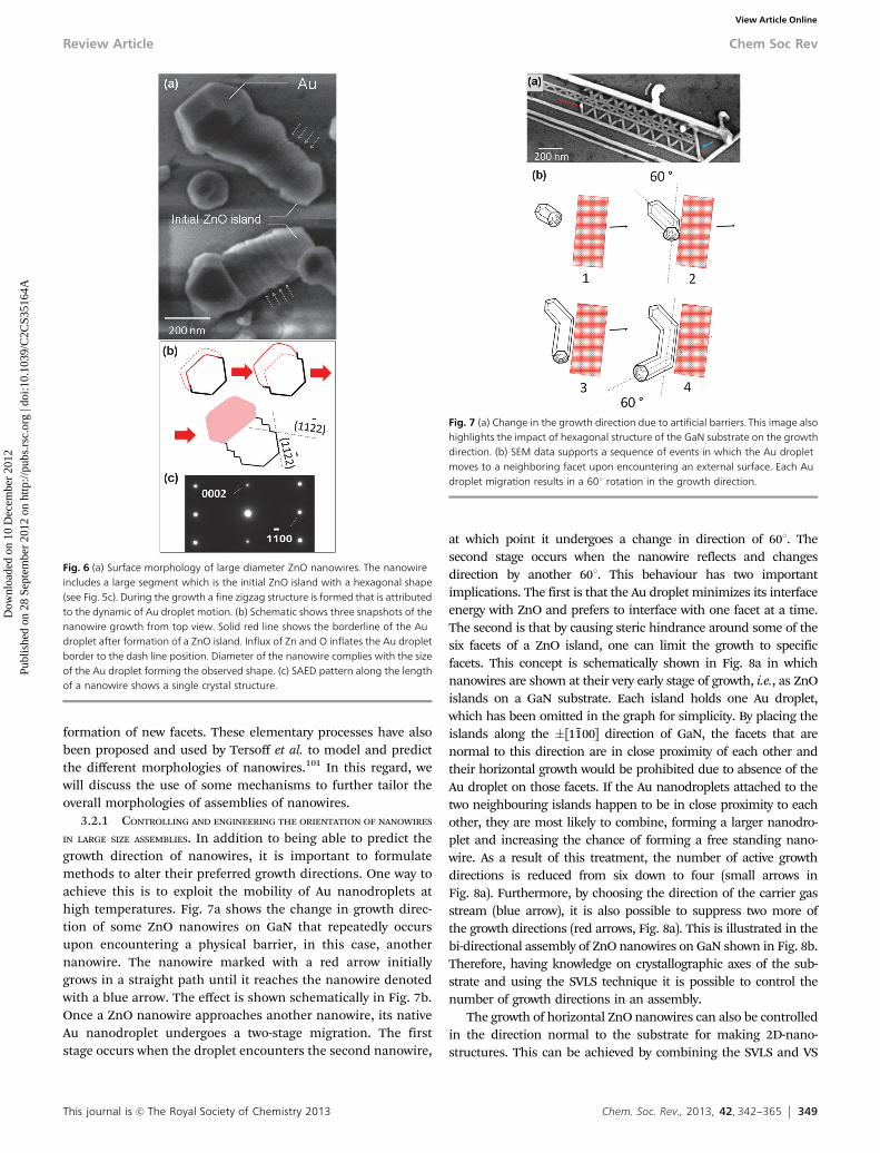
including: (1) existence of the native silicon oxide layer between Siand ZnO during the growth process; (2) 3% lattice mismatchbetween ZnO (a = 0.3249 nm) and Si (a = b = c = 0.5381 nm); (3)difference in crystal symmetries, i.e., cubic crystal symmetry of Siversus hexagonal crystal symmetry of ZnO. In growth of horizontalMg2SiO4 nanowires on silicon, a 1 nm thin amorphous layer isobserved at the interface, but it does not obstruct the influence ofthe substrate on the growth direction and despite E5% latticemismatch the epitaxial growth continues following the symmetriesof both cubic crystals.93 The influence of the substrate symmetryand epitaxial growth can be overridden by using artificial surfacesteps and grooves. In this regard it is shown that the fabricatednanosteps on a c-plane sapphire can force the GaN nanowires togrow along the steps and not those directions predicted by thehexagonal symmetries of both crystals.91 Another example high-lighting the significance of this relationship can be understoodfrom Fig. 4. This figure shows TiO2 nanowires grown on a GaNsubstrate that has been patterned with 10 nm-thick Au features.These nanowires are carbothermally grown from TiO2 powder(anatase phase) and as shown in Fig. 4a, demonstrate a growthdirection similar to that of ZnO on GaN, i.e., [1%100] direction.Based on the selected area electron diffraction (SAED) patterns inFig. 4b, the atomic packing in the TiO2 has a hexagonal structure(ABAB); however, there is a 301 crystal rotation in the TiO2
diffraction spots (highlighted with arrows), which is not observedin the ED pattern of ZnO nanowires in Fig. 4c.97
The directed planar growth of nanocrystals, based on theavailable models for anisotropic nanocrystal growth, can beexplained by the existence of an asymmetric lattice match between
Fig. 2 Hexagonal crystal structure of sapphire and orientation of its a-plane withrespect to the [0001] direction. Horizontal ZnO nanowires grow on the a-plane inthe [1 %100] direction.
Fig. 3 Impact of the substrate on directionality of horizontally grown nanowires.(a) ZnO nanowires grown on (0001) GaN illustrate multiple growth directionswith a 6-fold symmetry; while on a (001) silicon substrate (b) nanowires show noclear directionality.
Fig. 4 (a) Horizontal TiO2 nanowires grown from Au patterns on (0001) GaN. Thehighlighted crystallographic axes coincide with two growth directions. (b) SAEDpattern of TiO2 nanowires on GaN. (c) SAED pattern of ZnO nanowires on GaN.Both patterns are collected at the [0001] zone axis. The diffraction spots shownwith arrows in (b) indicate a 301 rotation in the crystal orientation for TiO2 withrespect to ZnO.
Review Article Chem Soc Rev
Dow
nloa
ded
on 1
0 D
ecem
ber
2012
Publ
ishe
d on
28
Sept
embe
r 20
12 o
n ht
tp://
pubs
.rsc
.org
| do
i:10.
1039
/C2C
S351
64A
View Article Online
348 Chem. Soc. Rev., 2013, 42, 342--365 This journal is c The Royal Society of Chemistry 2013
the epilayer and the host substrate.71 Based on this model, theobserved nanowire growth directions in the SVLS process could beindicative of the presence of high lattice match pathways betweenthe two crystals. However, the presence of these preferred direc-tions cannot be supported by the aforementioned examples asthey include highly matched (1.8% mismatch in ZnO and GaN)and highly mismatched crystals (75% mismatch in c-plane ZnOon a-plane sapphire). As such, the results indicate a loosedependence between crystal lattice match and the directionalityof the lateral growth. On the other hand, the crystal symmetry ofthe two crystals seems to be more influential in defining thenumber of growth directions.
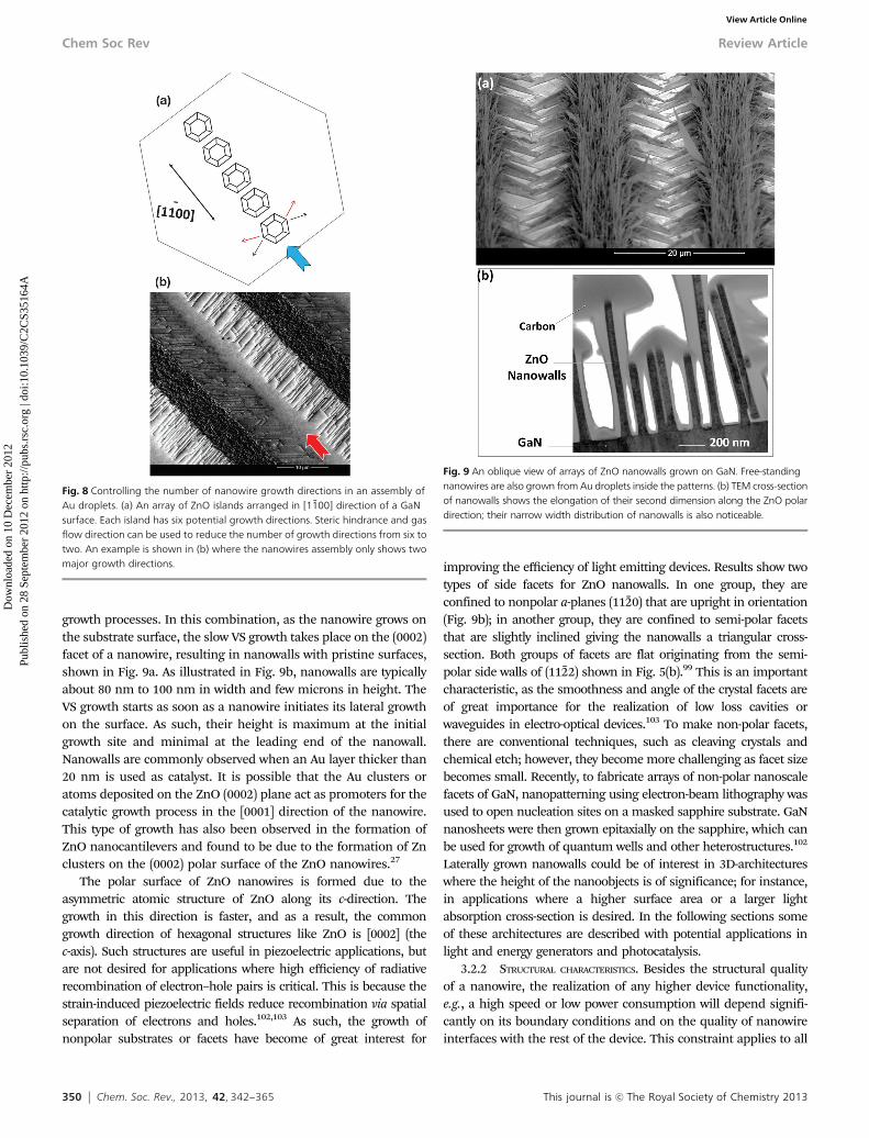
Examination of the interface between ZnO nanowires and thesapphire substrate by high-resolution transmission electron micro-scopy (HR-TEM) reveals a large compressive strain in the substrate.The representative image in Fig. 5a shows the deformation ofthe interface due to this strain.98 This observation opposes theexistence of low strain paths along the growth directions accordingto the model above.98 In the better matched case of ZnO on GaN,this stress is significantly reduced when viewed from the cross-section (Fig. 5b); however, from top view, when their c-planes areoverlapped, no lattice match in any crystallographic direction isobserved.99 Instead a local lattice match is observed, where itscoherency is maintained over a range of a few nanometers.99 Thismeans that a ZnO island can be formed epitaxially, but its epitaxialelongation is constrained due to the absence of a long-range lattice
match with the substrate. This contradiction can be resolved bytreating the SVLS process as a sequential island growth mechanism.At the early stage of the growth, a ZnO island100 is first formed at theinterface between the Au nanodroplet and the substrate (Fig. 5c). Asseen, the ZnO island with a hexagonal structure contains a (0001)polar face that is typically surrounded by six side facets. As explainedlater, results indicate that the Au droplet most likely wets half thesides of the ZnO island, which in Fig. 5c are under the Au. Two ofthese side facets can be seen in the HR-TEM cross-sectional imageof Fig. 5b. Based on the SAED pattern in Fig. 5d, the side facets are(11%22) that are about 321 tilted with respect to the ZnO a-plane(Fig. 2). The horizontal nanowires tend to exhibit triangular cross-sections that become trapezoidal due to the presence of a (0001)facet. Both SEM and the studied cross-sections (Fig. 5b) show thatthe (0001) polar facet has a smaller surface area than the side facets.This may explain why an Au nanodroplet prefers migrating to sidefacet(s) instead of preferentially wetting the top polar facet. The Aunanodroplet also stays partially in contact with the GaN surface,which enables nucleation of the 2nd ZnO island. Repetition of theserial island growth eventually leads to the elongation of the ZnOnanocrystal in �[0110] direction, a characteristic that is notnaturally observed for ZnO nanowires and other hexagonalcrystals. HRTEM cross-sectional microscopy shows a ripplednanowire surface, which most likely mean a subtle increase anddecrease in height of the nanowire as the Au droplet movesforward.99 This fluctuation in height could infer an inflation anddeflation of the Au nanodroplet most likely due to build-up anddepletion of the ZnO in the Au nanodroplet solution, respectively.This effect can be better observed in larger diameter nanowires viascanning electron microscopy (SEM) as illustrated in Fig. 6a. Thezigzag structure further shows the impact of variation in the Audroplet volume on the nanowire surface. In Fig. 6b, the red solidand dash lines in the first drawing represent the Au dropletborderlines before and after its inflation due to ZnO build-up,respectively; by continuing the growth, the inflated Au dropletleaves behind a ZnO nanocrystal and shrinks in size. From SEMobservations it can also be inferred that the Au droplet interfaceswith three adjacent non-polar ZnO facets among which the contactwith the left and right facets are partial. As the Au droplet increases(decreases) in volume its interface with these two facets increases(decreases) leading to the appearance of (11%22) facets. The size ofthese facets remains proportional to the change in Au dropletvolume, which seems to be small. Despite the sequential growth,examining the crystal structure of nanowires and SAED patternsalong their length (Fig. 6c) shows that the ZnO is single crystalline.In Fig. 6a, the observed structural deformation seen in the topnanowire (its right side) is due to the merge of its Au droplet withanother one during its surface travel.
Our results as well as others demonstrate that the direction-ality of nanowires in the SVLS process is a universal character-istic and can be predictable. It is of great interest to be able toselectively control the growth rate of these facets for realizationof desired nanostructures. As described above, the shape of theinitial semiconductor island is a crucial factor in defining thefate of a nanostructure’s morphology; it largely determines otherbasic characteristics such as facet growth, droplet position, and
Fig. 5 Surface and interface morphologies of ZnO nanowires on sapphire andGaN. (a) Cross-section of a ZnO nanowire on a-sapphire. Sapphire deformsunderneath the nanowire. (b) Cross-section of a ZnO nanowire on GaN. Herewith a better lattice match, substrate deformation is not detectable. (c) Thetop view schematic of the initial ZnO island is expected to have six non-polar(11 %22) facets. Au interfaces with three of these side facets from which themiddle one has a higher growth rate determining the direction of the nanowire(red arrow). (d) SAED pattern of the nanowire segment in part (b) shows[000 %2] and [11 %22] directions of the nanowire and GaN.
Chem Soc Rev Review Article
Dow
nloa
ded
on 1
0 D
ecem
ber
2012
Publ
ishe
d on
28
Sept
embe
r 20
12 o
n ht
tp://
pubs
.rsc
.org
| do
i:10.
1039
/C2C
S351
64A
View Article Online
This journal is c The Royal Society of Chemistry 2013 Chem. Soc. Rev., 2013, 42, 342--365 349
formation of new facets. These elementary processes have alsobeen proposed and used by Tersoff et al. to model and predictthe different morphologies of nanowires.101 In this regard, wewill discuss the use of some mechanisms to further tailor theoverall morphologies of assemblies of nanowires.
3.2.1 CONTROLLING AND ENGINEERING THE ORIENTATION OF NANOWIRES
IN LARGE SIZE ASSEMBLIES. In addition to being able to predict thegrowth direction of nanowires, it is important to formulatemethods to alter their preferred growth directions. One way toachieve this is to exploit the mobility of Au nanodroplets athigh temperatures. Fig. 7a shows the change in growth direc-tion of some ZnO nanowires on GaN that repeatedly occursupon encountering a physical barrier, in this case, anothernanowire. The nanowire marked with a red arrow initiallygrows in a straight path until it reaches the nanowire denotedwith a blue arrow. The effect is shown schematically in Fig. 7b.Once a ZnO nanowire approaches another nanowire, its nativeAu nanodroplet undergoes a two-stage migration. The firststage occurs when the droplet encounters the second nanowire,
at which point it undergoes a change in direction of 601. Thesecond stage occurs when the nanowire reflects and changesdirection by another 601. This behaviour has two importantimplications. The first is that the Au droplet minimizes its interfaceenergy with ZnO and prefers to interface with one facet at a time.The second is that by causing steric hindrance around some of thesix facets of a ZnO island, one can limit the growth to specificfacets. This concept is schematically shown in Fig. 8a in whichnanowires are shown at their very early stage of growth, i.e., as ZnOislands on a GaN substrate. Each island holds one Au droplet,which has been omitted in the graph for simplicity. By placing theislands along the �[1%100] direction of GaN, the facets that arenormal to this direction are in close proximity of each other andtheir horizontal growth would be prohibited due to absence of theAu droplet on those facets. If the Au nanodroplets attached to thetwo neighbouring islands happen to be in close proximity to eachother, they are most likely to combine, forming a larger nanodro-plet and increasing the chance of forming a free standing nano-wire. As a result of this treatment, the number of active growthdirections is reduced from six down to four (small arrows inFig. 8a). Furthermore, by choosing the direction of the carrier gasstream (blue arrow), it is also possible to suppress two more ofthe growth directions (red arrows, Fig. 8a). This is illustrated in thebi-directional assembly of ZnO nanowires on GaN shown in Fig. 8b.Therefore, having knowledge on crystallographic axes of the sub-strate and using the SVLS technique it is possible to control thenumber of growth directions in an assembly.
The growth of horizontal ZnO nanowires can also be controlledin the direction normal to the substrate for making 2D-nano-structures. This can be achieved by combining the SVLS and VS
Fig. 7 (a) Change in the growth direction due to artificial barriers. This image alsohighlights the impact of hexagonal structure of the GaN substrate on the growthdirection. (b) SEM data supports a sequence of events in which the Au dropletmoves to a neighboring facet upon encountering an external surface. Each Audroplet migration results in a 601 rotation in the growth direction.
Fig. 6 (a) Surface morphology of large diameter ZnO nanowires. The nanowireincludes a large segment which is the initial ZnO island with a hexagonal shape(see Fig. 5c). During the growth a fine zigzag structure is formed that is attributedto the dynamic of Au droplet motion. (b) Schematic shows three snapshots of thenanowire growth from top view. Solid red line shows the borderline of the Audroplet after formation of a ZnO island. Influx of Zn and O inflates the Au dropletborder to the dash line position. Diameter of the nanowire complies with the sizeof the Au droplet forming the observed shape. (c) SAED pattern along the lengthof a nanowire shows a single crystal structure.
Review Article Chem Soc Rev
Dow
nloa
ded
on 1
0 D
ecem
ber
2012
Publ
ishe
d on
28
Sept
embe
r 20
12 o
n ht
tp://
pubs
.rsc
.org
| do
i:10.
1039
/C2C
S351
64A
View Article Online
350 Chem. Soc. Rev., 2013, 42, 342--365 This journal is c The Royal Society of Chemistry 2013
growth processes. In this combination, as the nanowire grows onthe substrate surface, the slow VS growth takes place on the (0002)facet of a nanowire, resulting in nanowalls with pristine surfaces,shown in Fig. 9a. As illustrated in Fig. 9b, nanowalls are typicallyabout 80 nm to 100 nm in width and few microns in height. TheVS growth starts as soon as a nanowire initiates its lateral growthon the surface. As such, their height is maximum at the initialgrowth site and minimal at the leading end of the nanowall.Nanowalls are commonly observed when an Au layer thicker than20 nm is used as catalyst. It is possible that the Au clusters oratoms deposited on the ZnO (0002) plane act as promoters for thecatalytic growth process in the [0001] direction of the nanowire.This type of growth has also been observed in the formation ofZnO nanocantilevers and found to be due to the formation of Znclusters on the (0002) polar surface of the ZnO nanowires.27
The polar surface of ZnO nanowires is formed due to theasymmetric atomic structure of ZnO along its c-direction. Thegrowth in this direction is faster, and as a result, the commongrowth direction of hexagonal structures like ZnO is [0002] (thec-axis). Such structures are useful in piezoelectric applications, butare not desired for applications where high efficiency of radiativerecombination of electron–hole pairs is critical. This is because thestrain-induced piezoelectric fields reduce recombination via spatialseparation of electrons and holes.102,103 As such, the growth ofnonpolar substrates or facets have become of great interest for
improving the efficiency of light emitting devices. Results show twotypes of side facets for ZnO nanowalls. In one group, they areconfined to nonpolar a-planes (11%20) that are upright in orientation(Fig. 9b); in another group, they are confined to semi-polar facetsthat are slightly inclined giving the nanowalls a triangular cross-section. Both groups of facets are flat originating from the semi-polar side walls of (11%22) shown in Fig. 5(b).99 This is an importantcharacteristic, as the smoothness and angle of the crystal facets areof great importance for the realization of low loss cavities orwaveguides in electro-optical devices.103 To make non-polar facets,there are conventional techniques, such as cleaving crystals andchemical etch; however, they become more challenging as facet sizebecomes small. Recently, to fabricate arrays of non-polar nanoscalefacets of GaN, nanopatterning using electron-beam lithography wasused to open nucleation sites on a masked sapphire substrate. GaNnanosheets were then grown epitaxially on the sapphire, which canbe used for growth of quantum wells and other heterostructures.102
Laterally grown nanowalls could be of interest in 3D-architectureswhere the height of the nanoobjects is of significance; for instance,in applications where a higher surface area or a larger lightabsorption cross-section is desired. In the following sections someof these architectures are described with potential applications inlight and energy generators and photocatalysis.
3.2.2 STRUCTURAL CHARACTERISTICS. Besides the structural qualityof a nanowire, the realization of any higher device functionality,e.g., a high speed or low power consumption will depend signifi-cantly on its boundary conditions and on the quality of nanowireinterfaces with the rest of the device. This constraint applies to all
Fig. 9 An oblique view of arrays of ZnO nanowalls grown on GaN. Free-standingnanowires are also grown from Au droplets inside the patterns. (b) TEM cross-sectionof nanowalls shows the elongation of their second dimension along the ZnO polardirection; their narrow width distribution of nanowalls is also noticeable.
Fig. 8 Controlling the number of nanowire growth directions in an assembly ofAu droplets. (a) An array of ZnO islands arranged in [1 %100] direction of a GaNsurface. Each island has six potential growth directions. Steric hindrance and gasflow direction can be used to reduce the number of growth directions from six totwo. An example is shown in (b) where the nanowires assembly only shows twomajor growth directions.
Chem Soc Rev Review Article
Dow
nloa
ded
on 1
0 D
ecem
ber
2012
Publ
ishe
d on
28
Sept
embe
r 20
12 o
n ht
tp://
pubs
.rsc
.org
| do
i:10.
1039
/C2C
S351
64A
View Article Online
This journal is c The Royal Society of Chemistry 2013 Chem. Soc. Rev., 2013, 42, 342--365 351
the nanowires active in a device; as such it is important to be ableto reproduce similar interfaces as well as to control and predict theextent of their defects. In the in situ growth of horizontal nanowiresusing the SVLS method, since the interfaces of horizontal nano-wires are formed simultaneously, their structures are expected to bequite similar. This is an important feature that could enable qualitycontrol of a massive number of nanowire devices such as p–njunctions, quantum wells, or transistors in a short period of time.In this section we will describe some of our results on the crystalquality of laterally grown nanowires and nanowalls and theirinterfaces with substrates such as sapphire and GaN.
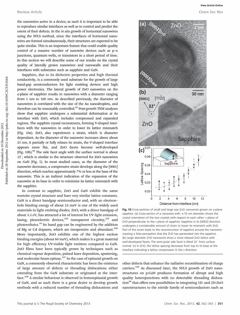
Sapphire, due to its dielectric properties and high thermalconductivity, is a commonly used substrate for the growth of largeband-gap semiconductors for light emitting devices and highpower electronics. The lateral growth of ZnO nanowires on thea-plane of sapphire results in nanowires with a diameter rangingfrom 1 nm to 100 nm. As described previously, the diameter ofnanowires is correlated with the size of the Au nanodroplets, andtherefore can be reasonably controlled.82 Post-growth TEM analysesshow that sapphire undergoes a substantial deformation at itsinterface with ZnO, which includes compressed and expandedregions. The sapphire crystal reconstructs, forming V-shaped inter-faces with the nanowires in order to lower its lattice mismatch(Fig. 10a). ZnO, also experiences a strain, which is diameterdependant. As the diameter of the nanowire increases above about25 nm, it partially or fully relaxes its strain, the V-shaped interfaceappears more flat, and ZnO facets become well-developed(Fig. 10b).99 The side facet angle with the surface normal is about321, which is similar to the structure observed for ZnO nanowireson GaN (Fig. 5). In most studied cases, as the diameter of thenanowire decreases, a compressive strain develops along the [0001]direction, which reaches approximately 7% or less at the base of thenanowire. This is an indirect indication of the expansion of thenanowire at its base in order to minimize its lattice mismatch withthe sapphire.
In contrast to sapphire, ZnO and GaN exhibit the samewurtzite crystal structure and have very similar lattice constants.GaN is a direct bandgap semiconductor and, with an electron–hole binding energy of about 24 meV is one of the widely usedmaterials in light emitting diodes. ZnO, with a direct bandgap ofabout 3.3 eV, has attracted a lot of interest for UV light emission,lasing, piezoelectric devices,104 transparent circuitry,105 andphotovoltaics.30 Its band gap can be engineered by the additionof Mg or Cd dopants, which are inexpensive and abundant.106
More importantly, ZnO exhibits one of the highest excitonbinding energies (about 60 meV), which makes it a great materialfor high efficiency UV-visible light emitters compared to GaN.ZnO films have been typically grown by techniques such aschemical vapour deposition, pulsed laser deposition, sputtering,and molecular beam epitaxy.107 In the case of epitaxial growth onGaN, a commonly observed characteristic has been the existenceof large amount of defects or threading dislocations eitherextending from the GaN substrate or originated at the inter-face.108 A similar behaviour is observed in homoepitaxial growthof GaN, and as such there is a great desire to develop growthmethods with a reduced number of threading dislocations and
other defects that enhance the radiative recombination of chargecarriers.109 As discussed later, the SVLS growth of ZnO nano-structures on p-GaN produces formation of abrupt and highquality heterojunctions with no detectable threading disloca-tion96 that offers new possibilities in integrating 1D- and 2D-ZnOnanostructures to the nitride family of semiconductors such as
Fig. 10 Cross-sections of small and large size ZnO nanowires grown on a-planesapphire. (a) Cross-section of a nanowire with E10 nm diameter shows thecrystal orientation of the two crystals with respect to each other: c-plane ofZnO perpendicular to the c-plane of sapphire. Sapphire in its [0003] directionundergoes a considerable amount of strain to lower its mismatch with ZnO.Part of this strain leads to the reconstruction of sapphire around the nanowirecreating a false perception that the ZnO has penetrated into the sapphire.(b) Large diameter ZnO nanowires show a more relaxed ZnO lattice withwell-developed facets. The semi-polar side facet is tilted 321 from surfacenormal. (c) In ZnO, the lattice spacing decreases from top to its base at theinterface indicating a lattice compression in the c-direction.
Review Article Chem Soc Rev
Dow
nloa
ded
on 1
0 D
ecem
ber
2012
Publ
ishe
d on
28
Sept
embe
r 20
12 o
n ht
tp://
pubs
.rsc
.org
| do
i:10.
1039
/C2C
S351
64A
View Article Online
352 Chem. Soc. Rev., 2013, 42, 342--365 This journal is c The Royal Society of Chemistry 2013
GaN or InGaN for realization of multi-color light sources at large- ornanoscales.
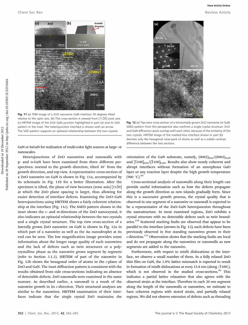
Heterojunctions of ZnO nanowires and nanowalls withp- and n-GaN have been examined from three different per-spectives: normal to the growth direction, tilted 301 from thegrowth direction, and top view. A representative cross-section ofa ZnO nanowire on GaN is shown in Fig. 11a, accompanied byits schematic in Fig. 11b for a better illustration. After thespecimen is tilted, the plane of view becomes (zone axis) [11%20]at which the ZnO plane spacing is larger, thus allowing foreasier detection of interface defects. Examining the ZnO–GaNheterojunctions using HRTEM shows a fairly coherent relation-ship at the interface (Fig. 11c). The SAED pattern shown in theinset shows the c- and m-directions of the ZnO nanocrystal; italso indicates an epitaxial relationship between the two crystalsand a single crystal structure. The top view cross-section of alaterally grown ZnO nanowire on GaN is shown in Fig. 12a inwhich part of a nanowire as well as the Au nanodroplet at itsend can be seen. The low magnification image provides someinformation about the longer range quality of such nanowiresand the lack of defects such as twin structures or a poly-crystalline phase as the nanowire grows segment by segment(refer to Section 3.1.3). HRTEM of part of the nanowire inFig. 12b shows the hexagonal order of atoms in the c-plane ofZnO and GaN. The inset diffraction pattern is consistent with theresults obtained from side cross-sections indicating an absenceof detectable defects. ZnO nanowalls were examined in the samemanner. As described earlier, a nanowall is a result of thenanowire growth in its c-direction. Their structural analyses aresimilar to the nanowires. HRTEM examination of their inter-faces indicate that the single crystal ZnO maintains the
orientation of the GaN substrate, namely, (0002)ZnOJ(0002)GaN
and [%1100]ZnOJ[%1100]GaN. Results also show nearly coherent andabrupt interfaces without formation of an amorphous GaOlayer or any reaction layer despite the high growth temperature(900 1C).99
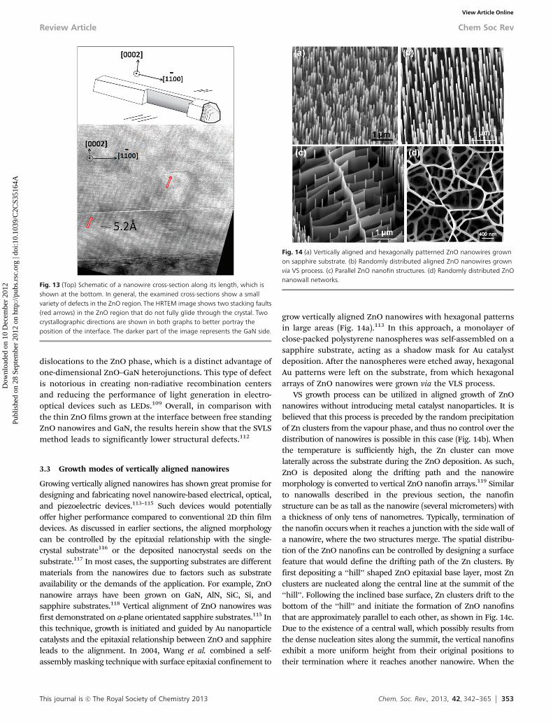
Cross-sectional analysis of nanowalls along their length canprovide useful information such as how the defects propagatealong the growth direction as new islands gradually form. Sincethis is a successive growth process, the crystal quality that isobserved in one segment of a nanowire or nanowall is expected tobe a representative of the ZnO–GaN heterojunction throughoutthe nanostructure. In most examined regions, ZnO exhibits acrystal structure with no detectable defects such as twin bound-aries.110 Scattered stacking faults are observed that appear to beparallel to the interface (arrows in Fig. 13); such defects have beenpreviously observed in free standing nanowires grown in theirc-direction.111 Observation shows that the stacking faults are localand do not propagate along the nanowires or nanowalls as newsegments are added to the nanowire.
Furthermore, with respect to misfit dislocations at the inter-face, we observe a small number of them. In a fully relaxed ZnOthin film on GaN, the 1.8% lattice mismatch is expected to resultin formation of misfit dislocations at every 15.8 nm (along h%1100i),which is not observed in the studied cross-sections.99 Thisindicates a partial lattice relaxation that also agrees with theobserved strain at the interface. Therefore in each 20 nm segmentalong the length of the nanowalls or nanowires, we estimate tohave coherent regions with stored strain, and partially relaxedregions. We did not observe extension of defects such as threading
Fig. 11 (a) TEM image of a ZnO nanowire–GaN interface 30 degrees tiltedrelative to the optic axis. (b) This cross-section is viewed from [11 %20] zone axis.(c) HRTEM image of the ZnO–GaN junction highlighted in part (a) and its SADpattern in the inset. The heterojunction interface is shown with an arrow.The SAD pattern supports an epitaxial relationship between the two crystals.
Fig. 12 (a) Top-view cross-section of a horizontally grown ZnO nanowire on GaN.SAED pattern from this perspective also confirms a single crystal structure. ZnOand GaN diffraction spots overlap with each other, because of the similarity of thetwo crystals. HRTEM image of the marked box interface shown in part (b)denotes only the hexagonal close-pack of atoms as well as a subtle contrastdifference between the two sections.
Chem Soc Rev Review Article
Dow
nloa
ded
on 1
0 D
ecem
ber
2012
Publ
ishe
d on
28
Sept
embe
r 20
12 o
n ht
tp://
pubs
.rsc
.org
| do
i:10.
1039
/C2C
S351
64A
View Article Online
This journal is c The Royal Society of Chemistry 2013 Chem. Soc. Rev., 2013, 42, 342--365 353
dislocations to the ZnO phase, which is a distinct advantage ofone-dimensional ZnO–GaN heterojunctions. This type of defectis notorious in creating non-radiative recombination centersand reducing the performance of light generation in electro-optical devices such as LEDs.109 Overall, in comparison withthe thin ZnO films grown at the interface between free standingZnO nanowires and GaN, the results herein show that the SVLSmethod leads to significantly lower structural defects.112
3.3 Growth modes of vertically aligned nanowires
Growing vertically aligned nanowires has shown great promise fordesigning and fabricating novel nanowire-based electrical, optical,and piezoelectric devices.113–115 Such devices would potentiallyoffer higher performance compared to conventional 2D thin filmdevices. As discussed in earlier sections, the aligned morphologycan be controlled by the epitaxial relationship with the single-crystal substrate116 or the deposited nanocrystal seeds on thesubstrate.117 In most cases, the supporting substrates are differentmaterials from the nanowires due to factors such as substrateavailability or the demands of the application. For example, ZnOnanowire arrays have been grown on GaN, AlN, SiC, Si, andsapphire substrates.118 Vertical alignment of ZnO nanowires wasfirst demonstrated on a-plane orientated sapphire substrates.115 Inthis technique, growth is initiated and guided by Au nanoparticlecatalysts and the epitaxial relationship between ZnO and sapphireleads to the alignment. In 2004, Wang et al. combined a self-assembly masking technique with surface epitaxial confinement to
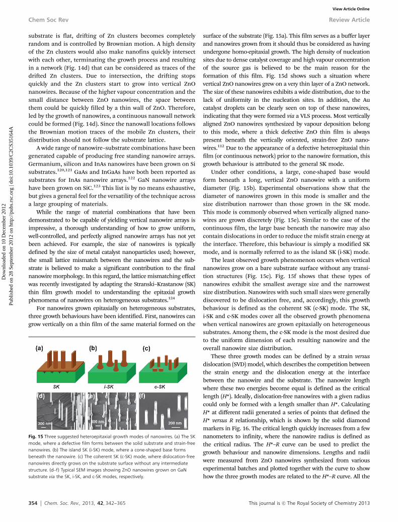
grow vertically aligned ZnO nanowires with hexagonal patternsin large areas (Fig. 14a).113 In this approach, a monolayer ofclose-packed polystyrene nanospheres was self-assembled on asapphire substrate, acting as a shadow mask for Au catalystdeposition. After the nanospheres were etched away, hexagonalAu patterns were left on the substrate, from which hexagonalarrays of ZnO nanowires were grown via the VLS process.
VS growth process can be utilized in aligned growth of ZnOnanowires without introducing metal catalyst nanoparticles. It isbelieved that this process is preceded by the random precipitationof Zn clusters from the vapour phase, and thus no control over thedistribution of nanowires is possible in this case (Fig. 14b). Whenthe temperature is sufficiently high, the Zn cluster can movelaterally across the substrate during the ZnO deposition. As such,ZnO is deposited along the drifting path and the nanowiremorphology is converted to vertical ZnO nanofin arrays.119 Similarto nanowalls described in the previous section, the nanofinstructure can be as tall as the nanowire (several micrometers) witha thickness of only tens of nanometres. Typically, termination ofthe nanofin occurs when it reaches a junction with the side wall ofa nanowire, where the two structures merge. The spatial distribu-tion of the ZnO nanofins can be controlled by designing a surfacefeature that would define the drifting path of the Zn clusters. Byfirst depositing a ‘‘hill’’ shaped ZnO epitaxial base layer, most Znclusters are nucleated along the central line at the summit of the‘‘hill’’. Following the inclined base surface, Zn clusters drift to thebottom of the ‘‘hill’’ and initiate the formation of ZnO nanofinsthat are approximately parallel to each other, as shown in Fig. 14c.Due to the existence of a central wall, which possibly results fromthe dense nucleation sites along the summit, the vertical nanofinsexhibit a more uniform height from their original positions totheir termination where it reaches another nanowire. When the
Fig. 13 (Top) Schematic of a nanowire cross-section along its length, which isshown at the bottom. In general, the examined cross-sections show a smallvariety of defects in the ZnO region. The HRTEM image shows two stacking faults(red arrows) in the ZnO region that do not fully glide through the crystal. Twocrystallographic directions are shown in both graphs to better portray theposition of the interface. The darker part of the image represents the GaN side.
Fig. 14 (a) Vertically aligned and hexagonally patterned ZnO nanowires grownon sapphire substrate. (b) Randomly distributed aligned ZnO nanowires grownvia VS process. (c) Parallel ZnO nanofin structures. (d) Randomly distributed ZnOnanowall networks.
Review Article Chem Soc Rev
Dow
nloa
ded
on 1
0 D
ecem
ber
2012
Publ
ishe
d on
28
Sept
embe
r 20
12 o
n ht
tp://
pubs
.rsc
.org
| do
i:10.
1039
/C2C
S351
64A
View Article Online
354 Chem. Soc. Rev., 2013, 42, 342--365 This journal is c The Royal Society of Chemistry 2013
substrate is flat, drifting of Zn clusters becomes completelyrandom and is controlled by Brownian motion. A high densityof the Zn clusters would also make nanofins quickly intersectwith each other, terminating the growth process and resultingin a network (Fig. 14d) that can be considered as traces of thedrifted Zn clusters. Due to intersection, the drifting stopsquickly and the Zn clusters start to grow into vertical ZnOnanowires. Because of the higher vapour concentration and thesmall distance between ZnO nanowires, the space betweenthem could be quickly filled by a thin wall of ZnO. Therefore,led by the growth of nanowires, a continuous nanowall networkcould be formed (Fig. 14d). Since the nanowall locations followsthe Brownian motion traces of the mobile Zn clusters, theirdistribution should not follow the substrate lattice.
A wide range of nanowire–substrate combinations have beengenerated capable of producing free standing nanowire arrays.Germanium, silicon and InAs nanowires have been grown on Sisubstrates.120,121 GaAs and InGaAs have both been reported assubstrates for InAs nanowire arrays.122 GaN nanowire arrayshave been grown on SiC.123 This list is by no means exhaustive,but gives a general feel for the versatility of the technique acrossa large grouping of materials.
While the range of material combinations that have beendemonstrated to be capable of yielding vertical nanowire arrays isimpressive, a thorough understanding of how to grow uniform,well-controlled, and perfectly aligned nanowire arrays has not yetbeen achieved. For example, the size of nanowires is typicallydefined by the size of metal catalyst nanoparticles used; however,the small lattice mismatch between the nanowires and the sub-strate is believed to make a significant contribution to the finalnanowire morphology. In this regard, the lattice mismatching effectwas recently investigated by adapting the Stranski–Krastanow (SK)thin film growth model to understanding the epitaxial growthphenomena of nanowires on heterogeneous substrates.124
For nanowires grown epitaxially on heterogeneous substrates,three growth behaviours have been identified. First, nanowires cangrow vertically on a thin film of the same material formed on the
surface of the substrate (Fig. 15a). This film serves as a buffer layerand nanowires grown from it should thus be considered as havingundergone homo-epitaxial growth. The high density of nucleationsites due to dense catalyst coverage and high vapour concentrationof the source gas is believed to be the main reason for theformation of this film. Fig. 15d shows such a situation wherevertical ZnO nanowires grew on a very thin layer of a ZnO network.The size of these nanowires exhibits a wide distribution, due to thelack of uniformity in the nucleation sites. In addition, the Aucatalyst droplets can be clearly seen on top of these nanowires,indicating that they were formed via a VLS process. Most verticallyaligned ZnO nanowires synthesized by vapour deposition belongto this mode, where a thick defective ZnO thin film is alwayspresent beneath the vertically oriented, strain-free ZnO nano-wires.112 Due to the appearance of a defective heteroepitaxial thinfilm (or continuous network) prior to the nanowire formation, thisgrowth behaviour is attributed to the general SK mode.
Under other conditions, a large, cone-shaped base wouldform beneath a long, vertical ZnO nanowire with a uniformdiameter (Fig. 15b). Experimental observations show that thediameter of nanowires grown in this mode is smaller and thesize distribution narrower than those grown in the SK mode.This mode is commonly observed when vertically aligned nano-wires are grown discretely (Fig. 15e). Similar to the case of thecontinuous film, the large base beneath the nanowire may alsocontain dislocations in order to reduce the misfit strain energy atthe interface. Therefore, this behaviour is simply a modified SKmode, and is normally referred to as the island SK (i-SK) mode.
The least observed growth phenomenon occurs when verticalnanowires grow on a bare substrate surface without any transi-tion structures (Fig. 15c). Fig. 15f shows that these types ofnanowires exhibit the smallest average size and the narrowestsize distribution. Nanowires with such small sizes were generallydiscovered to be dislocation free, and, accordingly, this growthbehaviour is defined as the coherent SK (c-SK) mode. The SK,i-SK and c-SK modes cover all the observed growth phenomenawhen vertical nanowires are grown epitaxially on heterogeneoussubstrates. Among them, the c-SK mode is the most desired dueto the uniform dimension of each resulting nanowire and theoverall nanowire size distribution.
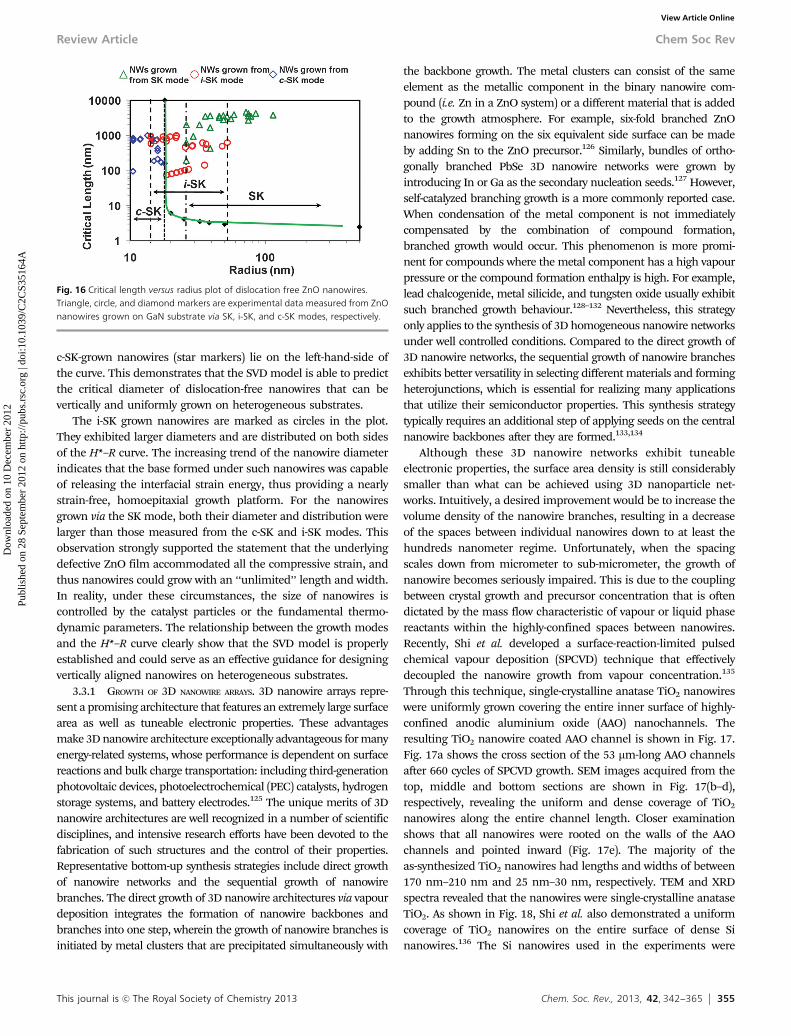
These three growth modes can be defined by a strain versusdislocation (SVD) model, which describes the competition betweenthe strain energy and the dislocation energy at the interfacebetween the nanowire and the substrate. The nanowire lengthwhere these two energies become equal is defined as the criticallength (H*). Ideally, dislocation-free nanowires with a given radiuscould only be formed with a length smaller than H*. CalculatingH* at different radii generated a series of points that defined theH* versus R relationship, which is shown by the solid diamondmarkers in Fig. 16. The critical length quickly increases from a fewnanometers to infinity, where the nanowire radius is defined asthe critical radius. The H*–R curve can be used to predict thegrowth behaviour and nanowire dimensions. Lengths and radiiwere measured from ZnO nanowires synthesized from variousexperimental batches and plotted together with the curve to showhow the three growth modes are related to the H*–R curve. All the
Fig. 15 Three suggested heteroepitaxial growth modes of nanowires. (a) The SKmode, where a defective film forms between the solid substrate and strain-freenanowires. (b) The island SK (i-SK) mode, where a cone-shaped base formsbeneath the nanowire. (c) The coherent SK (c-SK) mode, where dislocation-freenanowires directly grows on the substrate surface without any intermediatestructure. (d–f) Typical SEM images showing ZnO nanowires grown on GaNsubstrate via the SK, i-SK, and c-SK modes, respectively.
Chem Soc Rev Review Article
Dow
nloa
ded
on 1
0 D
ecem
ber
2012
Publ
ishe
d on
28
Sept
embe
r 20
12 o
n ht
tp://
pubs
.rsc
.org
| do
i:10.
1039
/C2C
S351
64A
View Article Online
This journal is c The Royal Society of Chemistry 2013 Chem. Soc. Rev., 2013, 42, 342--365 355
c-SK-grown nanowires (star markers) lie on the left-hand-side ofthe curve. This demonstrates that the SVD model is able to predictthe critical diameter of dislocation-free nanowires that can bevertically and uniformly grown on heterogeneous substrates.
The i-SK grown nanowires are marked as circles in the plot.They exhibited larger diameters and are distributed on both sidesof the H*–R curve. The increasing trend of the nanowire diameterindicates that the base formed under such nanowires was capableof releasing the interfacial strain energy, thus providing a nearlystrain-free, homoepitaxial growth platform. For the nanowiresgrown via the SK mode, both their diameter and distribution werelarger than those measured from the c-SK and i-SK modes. Thisobservation strongly supported the statement that the underlyingdefective ZnO film accommodated all the compressive strain, andthus nanowires could grow with an ‘‘unlimited’’ length and width.In reality, under these circumstances, the size of nanowires iscontrolled by the catalyst particles or the fundamental thermo-dynamic parameters. The relationship between the growth modesand the H*–R curve clearly show that the SVD model is properlyestablished and could serve as an effective guidance for designingvertically aligned nanowires on heterogeneous substrates.
3.3.1 GROWTH OF 3D NANOWIRE ARRAYS. 3D nanowire arrays repre-sent a promising architecture that features an extremely large surfacearea as well as tuneable electronic properties. These advantagesmake 3D nanowire architecture exceptionally advantageous for manyenergy-related systems, whose performance is dependent on surfacereactions and bulk charge transportation: including third-generationphotovoltaic devices, photoelectrochemical (PEC) catalysts, hydrogenstorage systems, and battery electrodes.125 The unique merits of 3Dnanowire architectures are well recognized in a number of scientificdisciplines, and intensive research efforts have been devoted to thefabrication of such structures and the control of their properties.Representative bottom-up synthesis strategies include direct growthof nanowire networks and the sequential growth of nanowirebranches. The direct growth of 3D nanowire architectures via vapourdeposition integrates the formation of nanowire backbones andbranches into one step, wherein the growth of nanowire branches isinitiated by metal clusters that are precipitated simultaneously with
the backbone growth. The metal clusters can consist of the sameelement as the metallic component in the binary nanowire com-pound (i.e. Zn in a ZnO system) or a different material that is addedto the growth atmosphere. For example, six-fold branched ZnOnanowires forming on the six equivalent side surface can be madeby adding Sn to the ZnO precursor.126 Similarly, bundles of ortho-gonally branched PbSe 3D nanowire networks were grown byintroducing In or Ga as the secondary nucleation seeds.127 However,self-catalyzed branching growth is a more commonly reported case.When condensation of the metal component is not immediatelycompensated by the combination of compound formation,branched growth would occur. This phenomenon is more promi-nent for compounds where the metal component has a high vapourpressure or the compound formation enthalpy is high. For example,lead chalcogenide, metal silicide, and tungsten oxide usually exhibitsuch branched growth behaviour.128–132 Nevertheless, this strategyonly applies to the synthesis of 3D homogeneous nanowire networksunder well controlled conditions. Compared to the direct growth of3D nanowire networks, the sequential growth of nanowire branchesexhibits better versatility in selecting different materials and formingheterojunctions, which is essential for realizing many applicationsthat utilize their semiconductor properties. This synthesis strategytypically requires an additional step of applying seeds on the centralnanowire backbones after they are formed.133,134
Although these 3D nanowire networks exhibit tuneableelectronic properties, the surface area density is still considerablysmaller than what can be achieved using 3D nanoparticle net-works. Intuitively, a desired improvement would be to increase thevolume density of the nanowire branches, resulting in a decreaseof the spaces between individual nanowires down to at least thehundreds nanometer regime. Unfortunately, when the spacingscales down from micrometer to sub-micrometer, the growth ofnanowire becomes seriously impaired. This is due to the couplingbetween crystal growth and precursor concentration that is oftendictated by the mass flow characteristic of vapour or liquid phasereactants within the highly-confined spaces between nanowires.Recently, Shi et al. developed a surface-reaction-limited pulsedchemical vapour deposition (SPCVD) technique that effectivelydecoupled the nanowire growth from vapour concentration.135
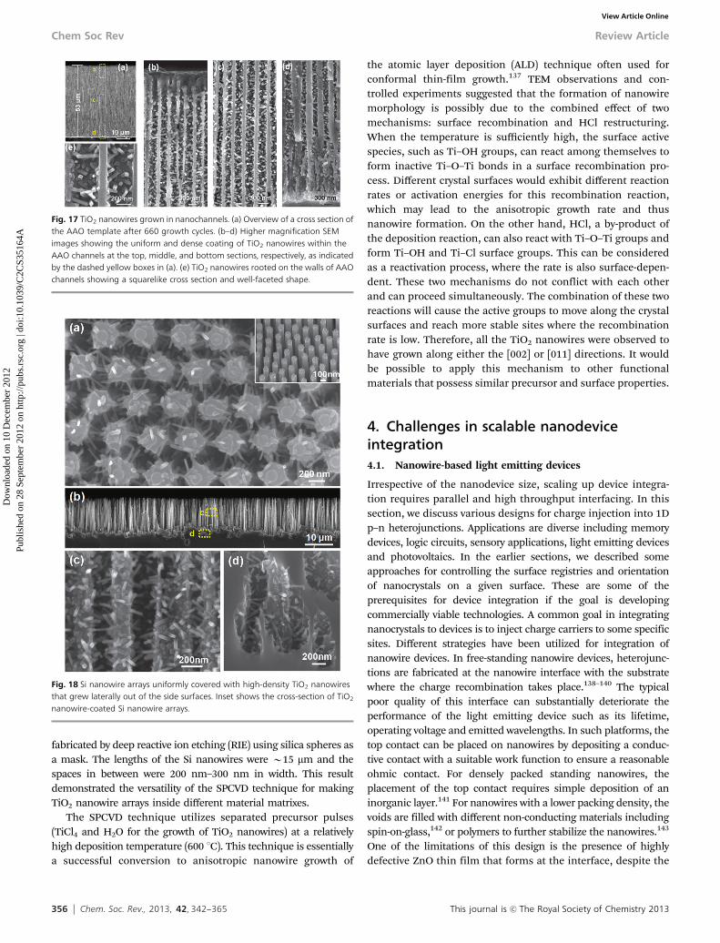
Through this technique, single-crystalline anatase TiO2 nanowireswere uniformly grown covering the entire inner surface of highly-confined anodic aluminium oxide (AAO) nanochannels. Theresulting TiO2 nanowire coated AAO channel is shown in Fig. 17.Fig. 17a shows the cross section of the 53 mm-long AAO channelsafter 660 cycles of SPCVD growth. SEM images acquired from thetop, middle and bottom sections are shown in Fig. 17(b–d),respectively, revealing the uniform and dense coverage of TiO2
nanowires along the entire channel length. Closer examinationshows that all nanowires were rooted on the walls of the AAOchannels and pointed inward (Fig. 17e). The majority of theas-synthesized TiO2 nanowires had lengths and widths of between170 nm–210 nm and 25 nm–30 nm, respectively. TEM and XRDspectra revealed that the nanowires were single-crystalline anataseTiO2. As shown in Fig. 18, Shi et al. also demonstrated a uniformcoverage of TiO2 nanowires on the entire surface of dense Sinanowires.136 The Si nanowires used in the experiments were
Fig. 16 Critical length versus radius plot of dislocation free ZnO nanowires.Triangle, circle, and diamond markers are experimental data measured from ZnOnanowires grown on GaN substrate via SK, i-SK, and c-SK modes, respectively.
Review Article Chem Soc Rev
Dow
nloa
ded
on 1
0 D
ecem
ber
2012
Publ
ishe
d on
28
Sept
embe
r 20
12 o
n ht
tp://
pubs
.rsc
.org
| do
i:10.
1039
/C2C
S351
64A
View Article Online
356 Chem. Soc. Rev., 2013, 42, 342--365 This journal is c The Royal Society of Chemistry 2013
fabricated by deep reactive ion etching (RIE) using silica spheres asa mask. The lengths of the Si nanowires were B15 mm and thespaces in between were 200 nm–300 nm in width. This resultdemonstrated the versatility of the SPCVD technique for makingTiO2 nanowire arrays inside different material matrixes.
The SPCVD technique utilizes separated precursor pulses(TiCl4 and H2O for the growth of TiO2 nanowires) at a relativelyhigh deposition temperature (600 1C). This technique is essentiallya successful conversion to anisotropic nanowire growth of
the atomic layer deposition (ALD) technique often used forconformal thin-film growth.137 TEM observations and con-trolled experiments suggested that the formation of nanowiremorphology is possibly due to the combined effect of twomechanisms: surface recombination and HCl restructuring.When the temperature is sufficiently high, the surface activespecies, such as Ti–OH groups, can react among themselves toform inactive Ti–O–Ti bonds in a surface recombination pro-cess. Different crystal surfaces would exhibit different reactionrates or activation energies for this recombination reaction,which may lead to the anisotropic growth rate and thusnanowire formation. On the other hand, HCl, a by-product ofthe deposition reaction, can also react with Ti–O–Ti groups andform Ti–OH and Ti–Cl surface groups. This can be consideredas a reactivation process, where the rate is also surface-depen-dent. These two mechanisms do not conflict with each otherand can proceed simultaneously. The combination of these tworeactions will cause the active groups to move along the crystalsurfaces and reach more stable sites where the recombinationrate is low. Therefore, all the TiO2 nanowires were observed tohave grown along either the [002] or [011] directions. It wouldbe possible to apply this mechanism to other functionalmaterials that possess similar precursor and surface properties.
4. Challenges in scalable nanodeviceintegration4.1. Nanowire-based light emitting devices
Irrespective of the nanodevice size, scaling up device integra-tion requires parallel and high throughput interfacing. In thissection, we discuss various designs for charge injection into 1Dp–n heterojunctions. Applications are diverse including memorydevices, logic circuits, sensory applications, light emitting devicesand photovoltaics. In the earlier sections, we described someapproaches for controlling the surface registries and orientationof nanocrystals on a given surface. These are some of theprerequisites for device integration if the goal is developingcommercially viable technologies. A common goal in integratingnanocrystals to devices is to inject charge carriers to some specificsites. Different strategies have been utilized for integration ofnanowire devices. In free-standing nanowire devices, heterojunc-tions are fabricated at the nanowire interface with the substratewhere the charge recombination takes place.138–140 The typicalpoor quality of this interface can substantially deteriorate theperformance of the light emitting device such as its lifetime,operating voltage and emitted wavelengths. In such platforms, thetop contact can be placed on nanowires by depositing a conduc-tive contact with a suitable work function to ensure a reasonableohmic contact. For densely packed standing nanowires, theplacement of the top contact requires simple deposition of aninorganic layer.141 For nanowires with a lower packing density, thevoids are filled with different non-conducting materials includingspin-on-glass,142 or polymers to further stabilize the nanowires.143
One of the limitations of this design is the presence of highlydefective ZnO thin film that forms at the interface, despite the
Fig. 18 Si nanowire arrays uniformly covered with high-density TiO2 nanowiresthat grew laterally out of the side surfaces. Inset shows the cross-section of TiO2
nanowire-coated Si nanowire arrays.
Fig. 17 TiO2 nanowires grown in nanochannels. (a) Overview of a cross section ofthe AAO template after 660 growth cycles. (b–d) Higher magnification SEMimages showing the uniform and dense coating of TiO2 nanowires within theAAO channels at the top, middle, and bottom sections, respectively, as indicatedby the dashed yellow boxes in (a). (e) TiO2 nanowires rooted on the walls of AAOchannels showing a squarelike cross section and well-faceted shape.
Chem Soc Rev Review Article
Dow
nloa
ded
on 1
0 D
ecem
ber
2012
Publ
ishe
d on
28
Sept
embe
r 20
12 o
n ht
tp://
pubs
.rsc
.org
| do
i:10.
1039
/C2C
S351
64A
View Article Online
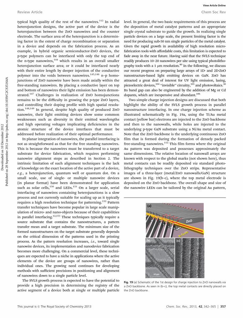
This journal is c The Royal Society of Chemistry 2013 Chem. Soc. Rev., 2013, 42, 342--365 357
typical high quality of the rest of the nanowires.112 In radialheterojunction designs, the active part of the device is theheterojunction between the ZnO nanowires and the counterelectrode. The surface area of the heterojunction is a determin-ing factor in the extent of charge recombination or separationin a device and depends on the fabrication process. As anexample, in hybrid organic semiconductor-ZnO devices, thep-type polymers can be interfaced with only the top end ofthe n-type nanowires,144 which results in an overall smallerheterojunction surface area; or it could be interfaced nearlywith their entire length by deeper injection of the conductivepolymer into the voids between nanowires.145,146 n–p homo-junctions of ZnO nanowire have been made axially within thefree-standing nanowires. By placing a conductive layer on topand bottom of nanowires their light emission has been demon-strated.147 Challenges in realization of ZnO homojunctionsremains to be the difficulty in growing the p-type ZnO layers,and controlling their doping profile with high spatial resolu-tion.148,149 In general, despite high quality of produced ZnOnanowire, their light emitting devices show some commonweaknesses such as diversity in their emitted wavelengthsand high operating voltages implicating deficiencies in theatomic structure of the device interfaces that must beaddressed before realization of their optimal performance.
In planar integration of nanowires, the parallel interfacing isnot as straightforward as that for the free standing nanowires.This is because the nanowires must be transferred to a targetsubstrate for device fabrication, which requires performingnanowire alignment steps as described in Section 2. Theintrinsic limitation of such alignment techniques is the lackof knowledge on the exact location of the active part of a device,e.g., a heterojunction, quantum well or quantum dot. On asmall scale, use of single- or multiple nanowire devices(in planar format) have been demonstrated for applicationsuch as solar cells,150 and LEDs.151 On a larger scale, serialinterfacing of nanowires containing heterojunctions is a slowprocess and not currently suitable for scaling up as it typicallyrequires a high resolution technique for patterning.152 Patterntransfer techniques have become popular in large scale manip-ulation of micro- and nano-objects because of their capabilitiesin parallel interfacing.12,153 These techniques typically require asource substrate that contains the nanostructures, a patterntransfer mean and a target substrate. The minimum size of theformed nanostructures on the target substrate generally dependson the critical dimension of the patterns used in the printingprocess. As the pattern resolution increases, i.e., toward singlenanowire devices, its implementation and nanodevice fabricationbecomes more challenging. On a commercial level, these techni-ques are expected to have a niche in applications where the activeelements of the device are groups of nanowires, rather thanindividual ones. The growing need continues for developingmethods with sufficient precisions in positioning and alignmentof nanowires down to a single particle level.
The SVLS growth process is expected to have the potential toprovide a high precision in determining the registry of theactive segment of a device both at single or multiple particle
level. In general, the two basic requirements of this process arethe deposition of metal catalyst patterns and an appropriatesingle crystal substrate to guide the growth. In realizing singleparticle devices on a large scale, the present limiting factor is theneed for producing sub-50 nm single particles of the metal catalyst.Given the rapid growth in availability of high resolution micro-fabrication tools with affordable costs, this limitation is expected tofade away in the near future. Having said that the SVLS techniquereadily produces 10–20 nanowires per site using typical photolitho-graphy tools with a 1 mm resolution.80 In the following, we discussour recent progress on preparing large arrays of 1D- and 2D-ZnOnanostructure-based light emitting devices on GaN. ZnO hasattracted a great deal of interest for UV light emission, lasing,piezoelectric devices,104 ‘‘invisible’’ circuitry,105 and photovoltaics.30
Its band gap can also be engineered by the addition of Mg or Cddopants, which are inexpensive and abundant.106
Two simple charge injection designs are discussed that bothhighlight the ability of the SVLS growth process in parallelnanostructure interfacing. In one charge injection scheme asillustrated schematically in Fig. 19a, using the Ti/Au metalcontact (yellow bar) electrons are injected to the ZnO backboneand then to the nanowalls, while holes are injected to theunderlying p-type GaN substrate using a Ni/Au metal contact.Note that the ZnO backbone is the underlying continuous ZnOfilm that is formed during the formation of densely packedfree-standing nanowires.112 This film forms where the originalAu pattern was deposited and possesses approximately thesame dimensions. The relative location of nanowall arrays areknown with respect to the global marks (not shown here), thusmetal contacts can be readily deposited via standard photo-lithography techniques over the ZnO strips. Representativeimages of a three-layer (metal/ZnO nanowalls/GaN) structureare shown in Fig. 19(b–c), where the top metal electrode isdeposited on the ZnO backbone. The overall shape and size ofthe nanowire LEDs can be tailored by the original Au pattern,
Fig. 19 (a) Schematic of the 1st design for charge injection to ZnO nanowalls viaa ZnO backbone. As seen in (b–c), the top metal contacts are directly placed onthe ZnO backbone.
Review Article Chem Soc Rev
Dow
nloa
ded
on 1
0 D
ecem
ber
2012
Publ
ishe
d on
28
Sept
embe
r 20
12 o
n ht
tp://
pubs
.rsc
.org
| do
i:10.
1039
/C2C
S351
64A
View Article Online
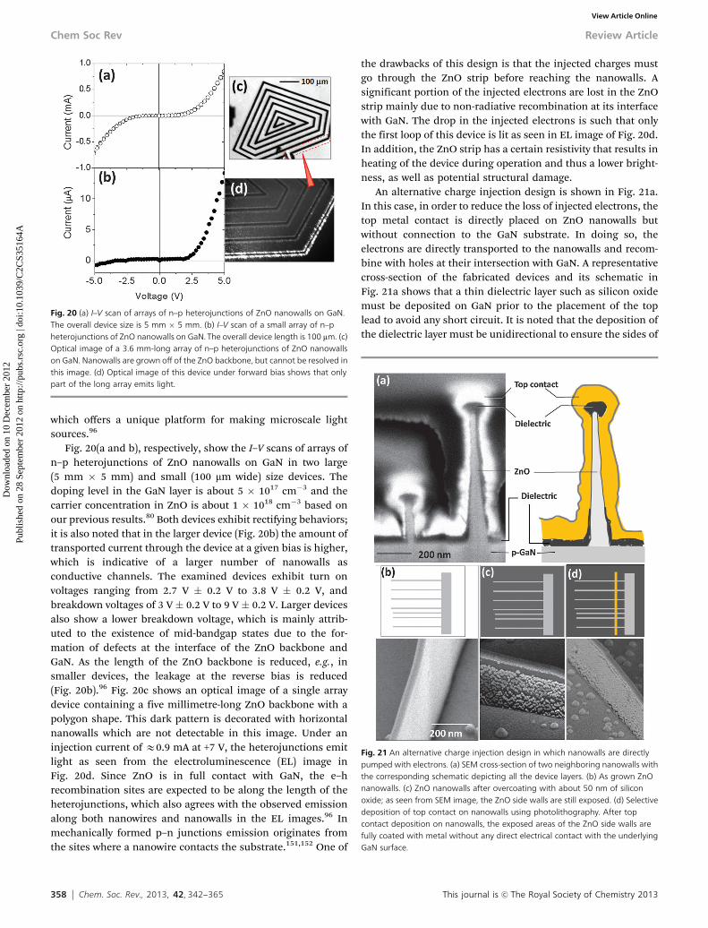
358 Chem. Soc. Rev., 2013, 42, 342--365 This journal is c The Royal Society of Chemistry 2013
which offers a unique platform for making microscale lightsources.96
Fig. 20(a and b), respectively, show the I–V scans of arrays ofn–p heterojunctions of ZnO nanowalls on GaN in two large(5 mm � 5 mm) and small (100 mm wide) size devices. Thedoping level in the GaN layer is about 5 � 1017 cm�3 and thecarrier concentration in ZnO is about 1 � 1018 cm�3 based onour previous results.80 Both devices exhibit rectifying behaviors;it is also noted that in the larger device (Fig. 20b) the amount oftransported current through the device at a given bias is higher,which is indicative of a larger number of nanowalls asconductive channels. The examined devices exhibit turn onvoltages ranging from 2.7 V � 0.2 V to 3.8 V � 0.2 V, andbreakdown voltages of 3 V � 0.2 V to 9 V � 0.2 V. Larger devicesalso show a lower breakdown voltage, which is mainly attrib-uted to the existence of mid-bandgap states due to the for-mation of defects at the interface of the ZnO backbone andGaN. As the length of the ZnO backbone is reduced, e.g., insmaller devices, the leakage at the reverse bias is reduced(Fig. 20b).96 Fig. 20c shows an optical image of a single arraydevice containing a five millimetre-long ZnO backbone with apolygon shape. This dark pattern is decorated with horizontalnanowalls which are not detectable in this image. Under aninjection current of E0.9 mA at +7 V, the heterojunctions emitlight as seen from the electroluminescence (EL) image inFig. 20d. Since ZnO is in full contact with GaN, the e–hrecombination sites are expected to be along the length of theheterojunctions, which also agrees with the observed emissionalong both nanowires and nanowalls in the EL images.96 Inmechanically formed p–n junctions emission originates fromthe sites where a nanowire contacts the substrate.151,152 One of
the drawbacks of this design is that the injected charges mustgo through the ZnO strip before reaching the nanowalls. Asignificant portion of the injected electrons are lost in the ZnOstrip mainly due to non-radiative recombination at its interfacewith GaN. The drop in the injected electrons is such that onlythe first loop of this device is lit as seen in EL image of Fig. 20d.In addition, the ZnO strip has a certain resistivity that results inheating of the device during operation and thus a lower bright-ness, as well as potential structural damage.
An alternative charge injection design is shown in Fig. 21a.In this case, in order to reduce the loss of injected electrons, thetop metal contact is directly placed on ZnO nanowalls butwithout connection to the GaN substrate. In doing so, theelectrons are directly transported to the nanowalls and recom-bine with holes at their intersection with GaN. A representativecross-section of the fabricated devices and its schematic inFig. 21a shows that a thin dielectric layer such as silicon oxidemust be deposited on GaN prior to the placement of the toplead to avoid any short circuit. It is noted that the deposition ofthe dielectric layer must be unidirectional to ensure the sides of
Fig. 20 (a) I–V scan of arrays of n–p heterojunctions of ZnO nanowalls on GaN.The overall device size is 5 mm � 5 mm. (b) I–V scan of a small array of n–pheterojunctions of ZnO nanowalls on GaN. The overall device length is 100 mm. (c)Optical image of a 3.6 mm-long array of n–p heterojunctions of ZnO nanowallson GaN. Nanowalls are grown off of the ZnO backbone, but cannot be resolved inthis image. (d) Optical image of this device under forward bias shows that onlypart of the long array emits light.
Fig. 21 An alternative charge injection design in which nanowalls are directlypumped with electrons. (a) SEM cross-section of two neighboring nanowalls withthe corresponding schematic depicting all the device layers. (b) As grown ZnOnanowalls. (c) ZnO nanowalls after overcoating with about 50 nm of siliconoxide; as seen from SEM image, the ZnO side walls are still exposed. (d) Selectivedeposition of top contact on nanowalls using photolithography. After topcontact deposition on nanowalls, the exposed areas of the ZnO side walls arefully coated with metal without any direct electrical contact with the underlyingGaN surface.
Chem Soc Rev Review Article
Dow
nloa
ded
on 1
0 D
ecem
ber
2012
Publ
ishe
d on
28
Sept
embe
r 20
12 o
n ht
tp://
pubs
.rsc
.org
| do
i:10.
1039
/C2C
S351
64A
View Article Online
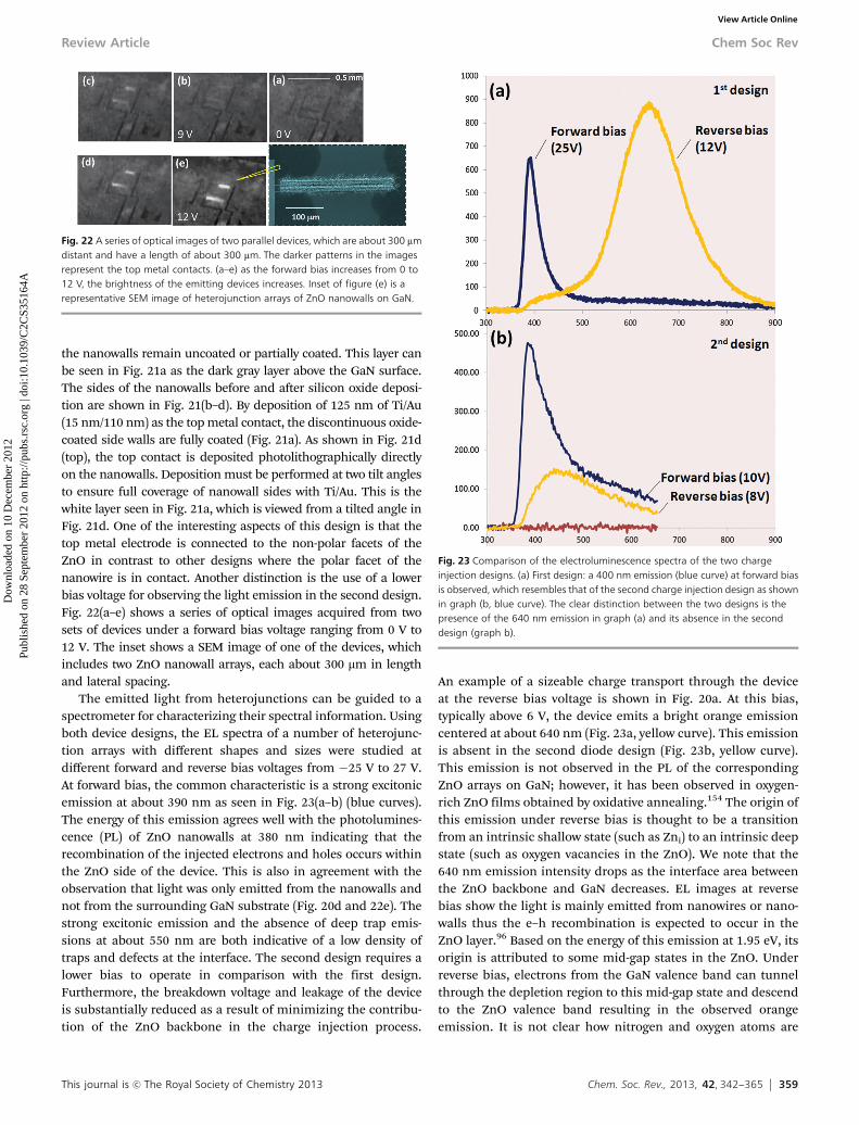
This journal is c The Royal Society of Chemistry 2013 Chem. Soc. Rev., 2013, 42, 342--365 359
the nanowalls remain uncoated or partially coated. This layer canbe seen in Fig. 21a as the dark gray layer above the GaN surface.The sides of the nanowalls before and after silicon oxide deposi-tion are shown in Fig. 21(b–d). By deposition of 125 nm of Ti/Au(15 nm/110 nm) as the top metal contact, the discontinuous oxide-coated side walls are fully coated (Fig. 21a). As shown in Fig. 21d(top), the top contact is deposited photolithographically directlyon the nanowalls. Deposition must be performed at two tilt anglesto ensure full coverage of nanowall sides with Ti/Au. This is thewhite layer seen in Fig. 21a, which is viewed from a tilted angle inFig. 21d. One of the interesting aspects of this design is that thetop metal electrode is connected to the non-polar facets of theZnO in contrast to other designs where the polar facet of thenanowire is in contact. Another distinction is the use of a lowerbias voltage for observing the light emission in the second design.Fig. 22(a–e) shows a series of optical images acquired from twosets of devices under a forward bias voltage ranging from 0 V to12 V. The inset shows a SEM image of one of the devices, whichincludes two ZnO nanowall arrays, each about 300 mm in lengthand lateral spacing.
The emitted light from heterojunctions can be guided to aspectrometer for characterizing their spectral information. Usingboth device designs, the EL spectra of a number of heterojunc-tion arrays with different shapes and sizes were studied atdifferent forward and reverse bias voltages from �25 V to 27 V.At forward bias, the common characteristic is a strong excitonicemission at about 390 nm as seen in Fig. 23(a–b) (blue curves).The energy of this emission agrees well with the photolumines-cence (PL) of ZnO nanowalls at 380 nm indicating that therecombination of the injected electrons and holes occurs withinthe ZnO side of the device. This is also in agreement with theobservation that light was only emitted from the nanowalls andnot from the surrounding GaN substrate (Fig. 20d and 22e). Thestrong excitonic emission and the absence of deep trap emis-sions at about 550 nm are both indicative of a low density oftraps and defects at the interface. The second design requires alower bias to operate in comparison with the first design.Furthermore, the breakdown voltage and leakage of the deviceis substantially reduced as a result of minimizing the contribu-tion of the ZnO backbone in the charge injection process.
An example of a sizeable charge transport through the deviceat the reverse bias voltage is shown in Fig. 20a. At this bias,typically above 6 V, the device emits a bright orange emissioncentered at about 640 nm (Fig. 23a, yellow curve). This emissionis absent in the second diode design (Fig. 23b, yellow curve).This emission is not observed in the PL of the correspondingZnO arrays on GaN; however, it has been observed in oxygen-rich ZnO films obtained by oxidative annealing.154 The origin ofthis emission under reverse bias is thought to be a transitionfrom an intrinsic shallow state (such as Zni) to an intrinsic deepstate (such as oxygen vacancies in the ZnO). We note that the640 nm emission intensity drops as the interface area betweenthe ZnO backbone and GaN decreases. EL images at reversebias show the light is mainly emitted from nanowires or nano-walls thus the e–h recombination is expected to occur in theZnO layer.96 Based on the energy of this emission at 1.95 eV, itsorigin is attributed to some mid-gap states in the ZnO. Underreverse bias, electrons from the GaN valence band can tunnelthrough the depletion region to this mid-gap state and descendto the ZnO valence band resulting in the observed orangeemission. It is not clear how nitrogen and oxygen atoms are
Fig. 22 A series of optical images of two parallel devices, which are about 300 mmdistant and have a length of about 300 mm. The darker patterns in the imagesrepresent the top metal contacts. (a–e) as the forward bias increases from 0 to12 V, the brightness of the emitting devices increases. Inset of figure (e) is arepresentative SEM image of heterojunction arrays of ZnO nanowalls on GaN.
Fig. 23 Comparison of the electroluminescence spectra of the two chargeinjection designs. (a) First design: a 400 nm emission (blue curve) at forward biasis observed, which resembles that of the second charge injection design as shownin graph (b, blue curve). The clear distinction between the two designs is thepresence of the 640 nm emission in graph (a) and its absence in the seconddesign (graph b).
Review Article Chem Soc Rev
Dow
nloa
ded
on 1
0 D
ecem
ber
2012
Publ
ishe
d on
28
Sept
embe
r 20
12 o
n ht
tp://
pubs
.rsc
.org
| do
i:10.
1039
/C2C
S351
64A
View Article Online
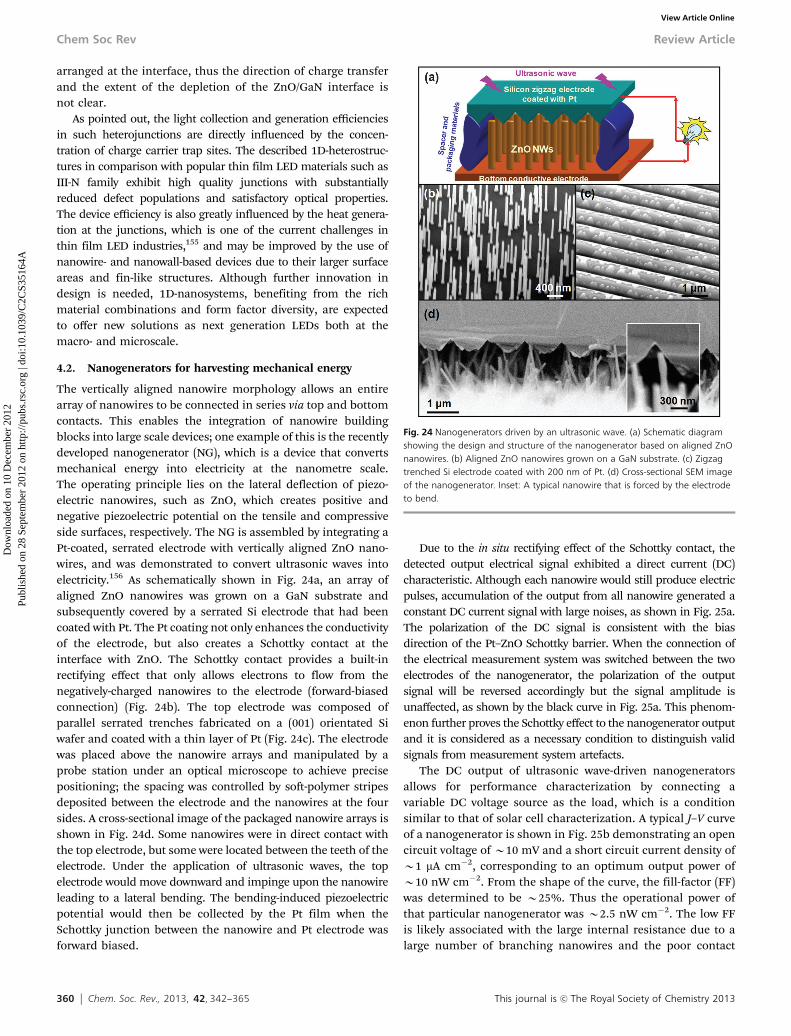
360 Chem. Soc. Rev., 2013, 42, 342--365 This journal is c The Royal Society of Chemistry 2013
arranged at the interface, thus the direction of charge transferand the extent of the depletion of the ZnO/GaN interface isnot clear.
As pointed out, the light collection and generation efficienciesin such heterojunctions are directly influenced by the concen-tration of charge carrier trap sites. The described 1D-heterostruc-tures in comparison with popular thin film LED materials such asIII-N family exhibit high quality junctions with substantiallyreduced defect populations and satisfactory optical properties.The device efficiency is also greatly influenced by the heat genera-tion at the junctions, which is one of the current challenges inthin film LED industries,155 and may be improved by the use ofnanowire- and nanowall-based devices due to their larger surfaceareas and fin-like structures. Although further innovation indesign is needed, 1D-nanosystems, benefiting from the richmaterial combinations and form factor diversity, are expectedto offer new solutions as next generation LEDs both at themacro- and microscale.
4.2. Nanogenerators for harvesting mechanical energy
The vertically aligned nanowire morphology allows an entirearray of nanowires to be connected in series via top and bottomcontacts. This enables the integration of nanowire buildingblocks into large scale devices; one example of this is the recentlydeveloped nanogenerator (NG), which is a device that convertsmechanical energy into electricity at the nanometre scale.The operating principle lies on the lateral deflection of piezo-electric nanowires, such as ZnO, which creates positive andnegative piezoelectric potential on the tensile and compressiveside surfaces, respectively. The NG is assembled by integrating aPt-coated, serrated electrode with vertically aligned ZnO nano-wires, and was demonstrated to convert ultrasonic waves intoelectricity.156 As schematically shown in Fig. 24a, an array ofaligned ZnO nanowires was grown on a GaN substrate andsubsequently covered by a serrated Si electrode that had beencoated with Pt. The Pt coating not only enhances the conductivityof the electrode, but also creates a Schottky contact at theinterface with ZnO. The Schottky contact provides a built-inrectifying effect that only allows electrons to flow from thenegatively-charged nanowires to the electrode (forward-biasedconnection) (Fig. 24b). The top electrode was composed ofparallel serrated trenches fabricated on a (001) orientated Siwafer and coated with a thin layer of Pt (Fig. 24c). The electrodewas placed above the nanowire arrays and manipulated by aprobe station under an optical microscope to achieve precisepositioning; the spacing was controlled by soft-polymer stripesdeposited between the electrode and the nanowires at the foursides. A cross-sectional image of the packaged nanowire arrays isshown in Fig. 24d. Some nanowires were in direct contact withthe top electrode, but some were located between the teeth of theelectrode. Under the application of ultrasonic waves, the topelectrode would move downward and impinge upon the nanowireleading to a lateral bending. The bending-induced piezoelectricpotential would then be collected by the Pt film when theSchottky junction between the nanowire and Pt electrode wasforward biased.
Due to the in situ rectifying effect of the Schottky contact, thedetected output electrical signal exhibited a direct current (DC)characteristic. Although each nanowire would still produce electricpulses, accumulation of the output from all nanowire generated aconstant DC current signal with large noises, as shown in Fig. 25a.The polarization of the DC signal is consistent with the biasdirection of the Pt–ZnO Schottky barrier. When the connection ofthe electrical measurement system was switched between the twoelectrodes of the nanogenerator, the polarization of the outputsignal will be reversed accordingly but the signal amplitude isunaffected, as shown by the black curve in Fig. 25a. This phenom-enon further proves the Schottky effect to the nanogenerator outputand it is considered as a necessary condition to distinguish validsignals from measurement system artefacts.
The DC output of ultrasonic wave-driven nanogeneratorsallows for performance characterization by connecting avariable DC voltage source as the load, which is a conditionsimilar to that of solar cell characterization. A typical J–V curveof a nanogenerator is shown in Fig. 25b demonstrating an opencircuit voltage of B10 mV and a short circuit current density ofB1 mA cm�2, corresponding to an optimum output power ofB10 nW cm�2. From the shape of the curve, the fill-factor (FF)was determined to be B25%. Thus the operational power ofthat particular nanogenerator was B2.5 nW cm�2. The low FFis likely associated with the large internal resistance due to alarge number of branching nanowires and the poor contact
Fig. 24 Nanogenerators driven by an ultrasonic wave. (a) Schematic diagramshowing the design and structure of the nanogenerator based on aligned ZnOnanowires. (b) Aligned ZnO nanowires grown on a GaN substrate. (c) Zigzagtrenched Si electrode coated with 200 nm of Pt. (d) Cross-sectional SEM imageof the nanogenerator. Inset: A typical nanowire that is forced by the electrodeto bend.
Chem Soc Rev Review Article
Dow
nloa
ded
on 1
0 D
ecem
ber
2012
Publ
ishe
d on
28
Sept
embe
r 20
12 o
n ht
tp://
pubs
.rsc
.org
| do
i:10.
1039
/C2C
S351
64A
View Article Online
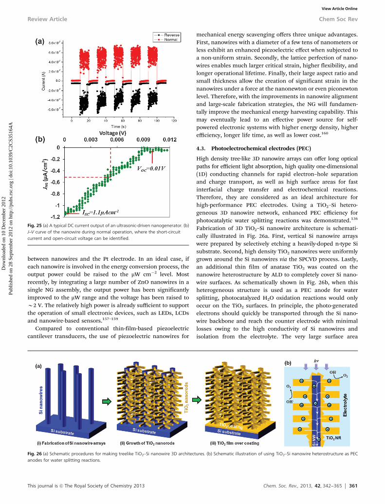
This journal is c The Royal Society of Chemistry 2013 Chem. Soc. Rev., 2013, 42, 342--365 361
between nanowires and the Pt electrode. In an ideal case, ifeach nanowire is involved in the energy conversion process, theoutput power could be raised to the mW cm�2 level. Mostrecently, by integrating a large number of ZnO nanowires in asingle NG assembly, the output power has been significantlyimproved to the mW range and the voltage has been raised toB2 V. The relatively high power is already sufficient to supportthe operation of small electronic devices, such as LEDs, LCDsand nanowire-based sensors.157–159
Compared to conventional thin-film-based piezoelectriccantilever transducers, the use of piezoelectric nanowires for
mechanical energy scavenging offers three unique advantages.First, nanowires with a diameter of a few tens of nanometers orless exhibit an enhanced piezoelectric effect when subjected toa non-uniform strain. Secondly, the lattice perfection of nano-wires enables much larger critical strain, higher flexibility, andlonger operational lifetime. Finally, their large aspect ratio andsmall thickness allow the creation of significant strain in thenanowires under a force at the nanonewton or even piconewtonlevel. Therefore, with the improvements in nanowire alignmentand large-scale fabrication strategies, the NG will fundamen-tally improve the mechanical energy harvesting capability. Thismay eventually lead to an effective power source for self-powered electronic systems with higher energy density, higherefficiency, longer life time, as well as lower cost.160
4.3. Photoelectrochemical electrodes (PEC)
High density tree-like 3D nanowire arrays can offer long opticalpaths for efficient light absorption, high quality one-dimensional(1D) conducting channels for rapid electron–hole separationand charge transport, as well as high surface areas for fastinterfacial charge transfer and electrochemical reactions.Therefore, they are considered as an ideal architecture forhigh-performance PEC electrodes. Using a TiO2–Si hetero-geneous 3D nanowire network, enhanced PEC efficiency forphotocatalytic water splitting reactions was demonstrated.136
Fabrication of 3D TiO2–Si nanowire architecture is schemati-cally illustrated in Fig. 26a. First, vertical Si nanowire arrayswere prepared by selectively etching a heavily-doped n-type Sisubstrate. Second, high density TiO2 nanowires were uniformlygrown around the Si nanowires via the SPCVD process. Lastly,an additional thin film of anatase TiO2 was coated on thenanowire heterostructure by ALD to completely cover Si nano-wire surfaces. As schematically shown in Fig. 26b, when thisheterogeneous structure is used as a PEC anode for watersplitting, photocatalyzed H2O oxidation reactions would onlyoccur on the TiO2 surfaces. In principle, the photo-generatedelectrons should quickly be transported through the Si nano-wire backbone and reach the counter electrode with minimallosses owing to the high conductivity of Si nanowires andisolation from the electrolyte. The very large surface area
Fig. 26 (a) Schematic procedures for making treelike TiO2–Si nanowire 3D architectures. (b) Schematic illustration of using TiO2–Si nanowire heterostructure as PECanodes for water splitting reactions.
Fig. 25 (a) A typical DC current output of an ultrasonic-driven nanogenerator. (b)J–V curve of the nanowire during normal operation, where the short-circuitcurrent and open-circuit voltage can be identified.
Review Article Chem Soc Rev
Dow
nloa
ded
on 1
0 D
ecem
ber
2012
Publ
ishe
d on
28
Sept
embe
r 20
12 o
n ht
tp://
pubs
.rsc
.org
| do
i:10.
1039
/C2C
S351
64A
View Article Online
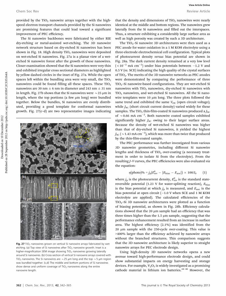
362 Chem. Soc. Rev., 2013, 42, 342--365 This journal is c The Royal Society of Chemistry 2013
provided by the TiO2 nanowire arrays together with the high-speed electron transport channels provided by the Si nanowiresare promising features that could lead toward a significantimprovement of PEC efficiency.
The Si nanowire backbones were fabricated by either RIEdry-etching or metal-assisted wet-etching. The 3D nanowirenetwork structure based on dry-etched Si nanowires has beenshown in Fig. 18. High density TiO2 nanowires were depositedon wet-etched Si nanowires. Fig. 27a is a planar view of a wet-etched Si nanowire forest after the growth of these nanowires.Closer examination showed that the Si nanowires were very thinand exhibited irregular cross sectional diameters as highlightedby yellow dashed circles in the inset of Fig. 27a. While the openspaces left within the bundling area were very small, the TiO2
nanowires could be found filling all these spaces. These TiO2
nanowires are 30 nm � 6 nm in diameter and 243 nm � 31 nmin length. Fig. 27b shows that the Si nanowires were B25 mm inlength, where the top portions (a few mm long) were bundledtogether. Below the bundles, Si nanowires are evenly distrib-uted, providing a good template for conformal nanowiresgrowth. Fig. 27(c–d) are two representative images indicating
that the density and dimensions of TiO2 nanowires were nearlyidentical at the middle and bottom regions. The nanowires grewlaterally from the Si nanowires and filled out the interspaces.Thus, a structure exhibiting a considerably large surface area aswell as high porosity was created by such a 3D architecture.
The TiO2–Si nanowire 3D architectures were then used as aPEC anode for water oxidation in a 1 M KOH electrolyte using athree-electrode electrochemical cell configuration. Typical plotsof photocurrent density versus bias potential are shown inFig. 28a. The dark current density remained at a very low level(o10�2 mA cm�2) under bias potentials between �1.2 V and0.5 V (vs. SCE) indicating the high quality of the crystal surfacesof TiO2. The merits of the 3D nanowire networks as PEC anodeswere demonstrated by comparing the performance of threeTiO2–Si nanowire-based configurations. They are wet-etched Sinanowires with TiO2 nanowires, dry-etched Si nanowires withTiO2 nanowires, and wet-etched Si nanowires. All the Si nano-wire templates were 10 mm long. The three plots followed thesame trend and exhibited the same VOC (open circuit voltage);while JSC (short circuit current density) varied widely for thesesamples. The TiO2 thin-film-coated Si nanowires produced a JSC
of B0.66 mA cm�2. Both nanowire coated samples exhibitedsignificantly higher JSC owing to their larger surface areas.Because the density of wet-etched Si nanowires was higherthan that of dry-etched Si nanowires, it yielded the highestJSC (B1.43 mA cm�2), which was more than twice that producedby the thin-film-coated sample.
The PEC performance was further investigated from various3D nanowire geometries, including different Si nanowirelengths and thickness of TiO2 over-coating (a necessary treat-ment in order to isolate Si from the electrolyte). From theresulting J–V curves, the PEC efficiencies were also evaluated viathe equation:
Z(photo)% = jp(E0rev � |Ebias � Eaoc|) � 100/I0 (1)
where jp is the photocurrent density, E0rev is the standard state-
reversible potential (1.23 V for water-splitting reaction), Ebias
is the bias potential at which jp is measured, and Eaoc is thebias potential at open circuit (�1.0 V when SCE and 1 M KOHelectrolyte are applied). The calculated efficiencies of theTiO2–Si 3D nanowire architectures were plotted as a functionof biasing potential, as shown in Fig. 28b. Efficiency calcula-tions showed that the 20 mm sample had an efficiency that wasthree times higher than the 1.5 mm sample, suggesting that theperformance enhancement resulted from an increase in surfacearea. The highest efficiency (2.1%) was identified from the20 mm sample with the 250-cycle over-coating. This value is>400% larger than the efficiency achieved by nanowire arrayswithout the branched structures. This comparison suggeststhat the 3D nanowire architecture is likely superior to straightnanowire arrays for PEC electrode design.
Using high-density 3D nanowire networks opens a newavenue toward high-performance electrode design, and couldshow substantial impacts on energy harvesting and storagedevices. For example, V2O5 is widely investigated as a promisingcathode material in lithium ion batteries.44–46 However, the
Fig. 27 TiO2 nanowires grown on vertical Si nanowire arrays fabricated by wetetching. (a) Top view of Si nanowires after TiO2 nanowire growth. Inset is ahigher-magnification SEM image showing TiO2 nanowires growing laterallyaround Si nanowires. (b) Cross-section of vertical Si nanowire arrays covered withTiO2 nanowires. The Si nanowires are B25 mm long and the top B5 mm regionwas bundled together. (c,d) The middle and bottom portions of Si nanowiresshow dense and uniform coverage of TiO2 nanowires along the entirenanowire length.
Chem Soc Rev Review Article
Dow
nloa
ded
on 1
0 D
ecem
ber
2012
Publ
ishe
d on
28
Sept
embe
r 20
12 o
n ht
tp://
pubs
.rsc
.org
| do
i:10.
1039
/C2C
S351
64A
View Article Online
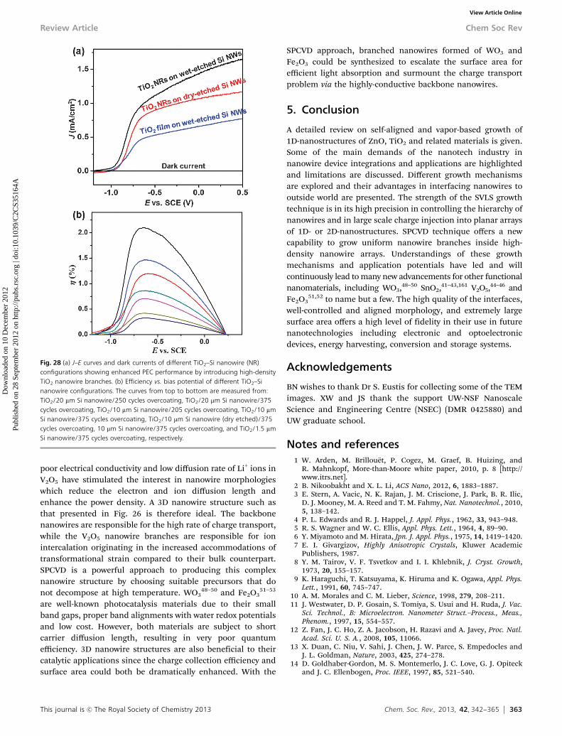
This journal is c The Royal Society of Chemistry 2013 Chem. Soc. Rev., 2013, 42, 342--365 363
poor electrical conductivity and low diffusion rate of Li+ ions inV2O5 have stimulated the interest in nanowire morphologieswhich reduce the electron and ion diffusion length andenhance the power density. A 3D nanowire structure such asthat presented in Fig. 26 is therefore ideal. The backbonenanowires are responsible for the high rate of charge transport,while the V2O5 nanowire branches are responsible for ionintercalation originating in the increased accommodations oftransformational strain compared to their bulk counterpart.SPCVD is a powerful approach to producing this complexnanowire structure by choosing suitable precursors that donot decompose at high temperature. WO3
48–50 and Fe2O351–53
are well-known photocatalysis materials due to their smallband gaps, proper band alignments with water redox potentialsand low cost. However, both materials are subject to shortcarrier diffusion length, resulting in very poor quantumefficiency. 3D nanowire structures are also beneficial to theircatalytic applications since the charge collection efficiency andsurface area could both be dramatically enhanced. With the
SPCVD approach, branched nanowires formed of WO3 andFe2O3 could be synthesized to escalate the surface area forefficient light absorption and surmount the charge transportproblem via the highly-conductive backbone nanowires.
5. Conclusion
A detailed review on self-aligned and vapor-based growth of1D-nanostructures of ZnO, TiO2 and related materials is given.Some of the main demands of the nanotech industry innanowire device integrations and applications are highlightedand limitations are discussed. Different growth mechanismsare explored and their advantages in interfacing nanowires tooutside world are presented. The strength of the SVLS growthtechnique is in its high precision in controlling the hierarchy ofnanowires and in large scale charge injection into planar arraysof 1D- or 2D-nanostructures. SPCVD technique offers a newcapability to grow uniform nanowire branches inside high-density nanowire arrays. Understandings of these growthmechanisms and application potentials have led and willcontinuously lead to many new advancements for other functionalnanomaterials, including WO3,48–50 SnO2,41–43,161 V2O5,44–46 andFe2O3
51,52 to name but a few. The high quality of the interfaces,well-controlled and aligned morphology, and extremely largesurface area offers a high level of fidelity in their use in futurenanotechnologies including electronic and optoelectronicdevices, energy harvesting, conversion and storage systems.
Acknowledgements
BN wishes to thank Dr S. Eustis for collecting some of the TEMimages. XW and JS thank the support UW-NSF NanoscaleScience and Engineering Centre (NSEC) (DMR 0425880) andUW graduate school.
Notes and references1 W. Arden, M. Brillouet, P. Cogez, M. Graef, B. Huizing, and
R. Mahnkopf, More-than-Moore white paper, 2010, p. 8 [http://www.itrs.net].
2 B. Nikoobakht and X. L. Li, ACS Nano, 2012, 6, 1883–1887.3 E. Stern, A. Vacic, N. K. Rajan, J. M. Criscione, J. Park, B. R. Ilic,
D. J. Mooney, M. A. Reed and T. M. Fahmy, Nat. Nanotechnol., 2010,5, 138–142.
4 P. L. Edwards and R. J. Happel, J. Appl. Phys., 1962, 33, 943–948.5 R. S. Wagner and W. C. Ellis, Appl. Phys. Lett., 1964, 4, 89–90.6 Y. Miyamoto and M. Hirata, Jpn. J. Appl. Phys., 1975, 14, 1419–1420.7 E. I. Givargizov, Highly Anisotropic Crystals, Kluwer Academic
Publishers, 1987.8 Y. M. Tairov, V. F. Tsvetkov and I. I. Khlebnik, J. Cryst. Growth,
1973, 20, 155–157.9 K. Haraguchi, T. Katsuyama, K. Hiruma and K. Ogawa, Appl. Phys.
Lett., 1991, 60, 745–747.10 A. M. Morales and C. M. Lieber, Science, 1998, 279, 208–211.11 J. Westwater, D. P. Gosain, S. Tomiya, S. Usui and H. Ruda, J. Vac.
Sci. Technol., B: Microelectron. Nanometer Struct.–Process., Meas.,Phenom., 1997, 15, 554–557.
12 Z. Fan, J. C. Ho, Z. A. Jacobson, H. Razavi and A. Javey, Proc. Natl.Acad. Sci. U. S. A., 2008, 105, 11066.
13 X. Duan, C. Niu, V. Sahi, J. Chen, J. W. Parce, S. Empedocles andJ. L. Goldman, Nature, 2003, 425, 274–278.
14 D. Goldhaber-Gordon, M. S. Montemerlo, J. C. Love, G. J. Opiteckand J. C. Ellenbogen, Proc. IEEE, 1997, 85, 521–540.
Fig. 28 (a) J–E curves and dark currents of different TiO2–Si nanowire (NR)configurations showing enhanced PEC performance by introducing high-densityTiO2 nanowire branches. (b) Efficiency vs. bias potential of different TiO2–Sinanowire configurations. The curves from top to bottom are measured from:TiO2/20 mm Si nanowire/250 cycles overcoating, TiO2/20 mm Si nanowire/375cycles overcoating, TiO2/10 mm Si nanowire/205 cycles overcoating, TiO2/10 mmSi nanowire/375 cycles overcoating, TiO2/10 mm Si nanowire (dry etched)/375cycles overcoating, 10 mm Si nanowire/375 cycles overcoating, and TiO2/1.5 mmSi nanowire/375 cycles overcoating, respectively.
Review Article Chem Soc Rev
Dow
nloa
ded
on 1
0 D
ecem
ber
2012
Publ
ishe
d on
28
Sept
embe
r 20
12 o
n ht
tp://
pubs
.rsc
.org
| do
i:10.
1039
/C2C
S351
64A
View Article Online
364 Chem. Soc. Rev., 2013, 42, 342--365 This journal is c The Royal Society of Chemistry 2013
15 F. Kim, S. Kwan, J. Akana and P. Yang, J. Am. Chem. Soc., 2001, 123,4360–4361.
16 B. Nikoobakht, Z. L. Wang and M. A. El-Sayed, J. Phys. Chem. B,2000, 104, 8635–8640.
17 G. Yu, A. Cao and C. M. Lieber, Nat. Nanotechnol., 2007, 2, 372–377.18 N. A. Melosh, A. Boukai, F. Diana, B. Gerardot, A. Badolato,
P. M. Petroff and J. R. Heath, Science, 2003, 300, 112–115.19 A. Javey, S. Woo, R. S. Friedman, H. Yan and C. M. Lieber, Nano
Lett., 2007, 7, 773–777.20 A. Pevzner, Y. Engel, R. Elnathan, T. Ducobni, M. Ben-Ishai,
K. Reddy, N. Shpaisman, A. Tsukernik, M. Oksman andF. Patolsky, Nano Lett., 2010, 10, 1202–1208.
21 E. Saeedi, C. Marcheselli, A. Shum and B. A. Parviz, Nanotechnology,2010, 21, 375604.
22 S. Xu, Y. Ding, Y. Wei, H. Fang, Y. Shen, A. K. Sood, D. L. Polla andZ. L. Wang, J. Am. Chem. Soc., 2009, 131, 6670–6671.
23 M. A. Meitl, Z. T. Zhu, V. Kumar, K. J. Lee, X. Feng, Y. Y. Huang,I. Adesida, R. G. Nuzzo and J. A. Rogers, Nat. Mater., 2006, 5, 33–38.
24 R. Yerushalmi, Z. A. Jacobson, J. C. Ho, Z. Fan and A. Javey, Appl.Phys. Lett., 2007, 91, 203104.
25 K. Takei, T. Takahashi, J. C. Ho, H. Ko, A. G. Gillies, P. W. Leu,R. S. Fearing and A. Javey, Nat. Mater., 2010, 9, 821–826.
26 S. A. Morin and S. Jin, Nano Lett., 2010, 10, 3459–3463.27 Z. L. Wang, X. Y. Kong and J. M. Zuo, Phys. Rev. Lett., 2003,
91, 185502.28 B. Gates, B. Mayers, B. Cattle and Y. N. Xia, Adv. Funct. Mater., 2002,
12, 219–227.29 H. Yu and W. E. Buhro, Adv. Mater., 2003, 15, 416–419.30 M. Law, L. E. Greene, J. C. Johnson, R. Saykally and P. Yang, Nat.
Mater., 2005, 4, 455–459.31 Y. Qin, R. Yang and Z. L. Wang, J. Phys. Chem. C, 2008, 112,
18734–18736.32 L. E. Greene, M. Law, D. H. Tan, M. Montano, J. Goldberger,
G. Somorjai and P. D. Yang, Nano Lett., 2005, 5, 1231–1236.33 X. J. Feng, K. Shankar, O. K. Varghese, M. Paulose, T. J. Latempa
and C. A. Grimes, Nano Lett., 2008, 8, 3781–3786.34 S. A. Morin, M. J. Bierman, J. Tong and S. Jin, Science, 2010, 328,
476–480.35 A. Fujishima and K. Honda, Nature, 1972, 238, 37–38.36 B. Oregan and M. Gratzel, Nature, 1991, 353, 737–740.37 S. Xu, Y. Qin, C. Xu, Y. G. Wei, R. S. Yang and Z. L. Wang, Nat.
Nanotechnol., 2010, 5, 366–373.38 S. Xu, Y. Wei, M. Kirkham, J. Liu, W. Mai, D. Davidovic, R. L. Snyder
and Z. L. Wang, J. Am. Chem. Soc., 2008, 130, 14958–14959.39 Y. G. Wei, W. Z. Wu, R. Guo, D. J. Yuan, S. M. Das and Z. L. Wang,
Nano Lett., 2010, 10, 3414–3419.40 J.-H. Ahn, Y.-J. Kim and G. Wang, J. Alloys Compd., 2009, 483, 422–424.41 A. Kolmakov, D. O. Klenov, Y. Lilach, S. Stemmer and
M. Moskovits, Nano Lett., 2005, 5, 667–673.42 S. H. Lee, G. Jo, W. Park, S. Lee, Y.-S. Kim, B. K. Cho, T. Lee and
W. B. Kim, ACS Nano, 2010, 4, 1829–1836.43 J. Pan, H. Shen, U. Werner, J. D. Prades, F. Hernandez-Ramirez,
F. Soldera, F. Mucklich and S. Mathur, J. Phys. Chem. C, 2011, 115,15191–15197.
44 H. Liu and W. Yang, Energy Environ. Sci., 2011, 4, 4000–4008.45 T. Zhai, H. Liu, H. Li, X. Fang, M. Liao, L. Li, H. Zhou, Y. Koide,
Y. Bando and D. Golberg, Adv. Mater., 2010, 22, 2547–2552.46 B. Yan, L. Liao, Y. You, X. Xu, Z. Zheng, Z. Shen, J. Ma, L. Tong and
T. Yu, Adv. Mater., 2009, 21, 2436–2440.47 C. Diaz-Guerra and J. Piqueras, J. Appl. Phys., 2007, 102,
084307–084304.48 H. Chen, N. Xu, S. Deng, J. Zhou, Z. Li, H. Ren, J. Chen and J. She,
J. Appl. Phys., 2007, 101, 114303–114305.49 Z. Gu, T. Zhai, B. Gao, X. Sheng, Y. Wang, H. Fu, Y. Ma and J. Yao,
J. Phys. Chem. B, 2006, 110, 23829–23836.50 J. Su, X. Feng, J. D. Sloppy, L. Guo and C. A. Grimes, Nano Lett.,
2010, 11, 203–208.51 Y. Fu, J. Chen and H. Zhang, Chem. Phys. Lett., 2001, 350, 491–494.52 G. Wang, X. Gou, J. Horvat and J. Park, J. Phys. Chem. C, 2008, 112,
15220–15225.53 P. M. Rao and X. Zheng, Nano Lett., 2009, 9, 3001–3006.54 M. T. Bjork, B. J. Ohlsson, T. Sass, A. I. Persson, C. Thelander,
M. H. Magnusson, K. Deppert, L. R. Wallenberg and L. Samuelson,Nano Lett., 2002, 2, 87–89.
55 F. Qian, Y. Li, S. Gradecak, H.-G. Park, Y. Dong, Y. Ding, Z. L. Wangand C. M. Lieber, Nat. Mater., 2008, 7, 701–706.
56 L. J. Lauhon, M. S. Gudiksen, D. Wang and C. M. Lieber, Nature,2002, 420, 57–61.
57 C. Yang, Z. Zhong and C. M. Lieber, Science, 2005, 310, 1304–1307.58 M. S. Gudiksen, L. J. Lauhon, J. Wang, D. C. Smith and
C. M. Lieber, Nature, 2002, 415, 617–620.59 X. Wang, J. Song, P. Li, J. H. Ryou, R. D. Dupuis, C. J. Summers and
Z. L. Wang, J. Am. Chem. Soc., 2005, 127, 7920–7923.60 B. Tian, P. Xie, T. J. Kempa, D. C. Bell and C. M. Lieber, Nat.
Nanotechnol., 2009, 4, 824–829.61 B. Xiang, P. Wang, X. Zhang, S. A. Dayeh, D. P. R. Aplin, C. Soci,
D. Yu and D. Wang, Nano Lett., 2006, 7, 323–328.62 Y. Wu, R. Fan and P. Yang, Nano Lett., 2002, 2, 83–86.63 S. A. Fortuna and X. L. Li, Semicond. Sci. Technol., 2010, 25, 24005.64 E. P. A. M. Bakkers, M. T. Borgstrom and M. A. Verheijen, MRS
Bull., 2007, 32, 5.65 L. C. Chuang, M. Moewe, C. Chase, N. P. Kobayashi, C. Chang-
Hasnain and S. Crankshaw, Appl. Phys. Lett., 2007, 90, 043115.66 Y. Wu, Y. Cui, L. Huynh, C. J. Barrelet, D. C. Bell and C. M. Lieber,
Nano Lett., 2004, 4, 433–436.67 C. X. Wang, M. Hirano and H. Hosono, Nano Lett., 2006, 6,
1552–1555.68 V. Schmidt, S. Senz and U. Gosele, Nano Lett., 2005, 5, 931–935.69 J. Stangl, V. Holy and G. Bauer, Rev. Mod. Phys., 2004, 76, 725–783.70 D. J. Eaglesham and M. Cerullo, Phys. Rev. Lett., 1990, 64, 1943.71 Y. Chen, D. A. A. Ohlberg, G. Medeiros-Ribeiro, Y. A. Chang and
R. S. Williams, Appl. Phys. Lett., 2000, 76, 4004–4006.72 Y. Chen, D. A. A. Ohlberg and R. S. Williams, J. Appl. Phys., 2002,
91, 3213–3218.73 D. Loretto, F. M. Ross and C. A. Lucas, Appl. Phys. Lett., 1996, 68,
2363–2365.74 Z. A. He, D. J. Smith and P. A. Bennett, Phys. Rev. Lett., 2004,
93, 256102.75 P. A. Bennett, Z. A. He, D. J. Smith and F. M. Ross, Thin Solid Films,
2011, 519, 8434–8440.76 E. I. Givargizov, J. Cryst. Growth, 2008, 310, 1686–1690.77 H. Ago, K. Nakamura, K. Ikeda, N. Uehara, N. Ishigami and
M. Tsuji, Chem. Phys. Lett., 2005, 408, 433–438.78 H. Ago, T. Nishi, K. Imamoto, N. Ishigami, M. Tsuji, T. Ikuta and
K. Takahashi, J. Phys. Chem. C, 114, 12925–12930.79 T. Ogino, H. Hibino, Y. Homma, Y. Kobayashi, K. Prabhakaran,
K. Sumitomo and H. Omi, Acc. Chem. Res., 1999, 32, 8.80 B. Nikoobakht, Chem. Mater., 2007, 19, 5279–5284.81 S. A. Fortuna, J. Wen, I. S. Chun and X. Li, Nano Lett., 2008, 8,
4421–4427.82 B. Nikoobakht, C. A. Michaels, S. J. Stranick and M. D. Vaudin,
Appl. Phys. Lett., 2004, 85, 3244–3246.83 Z. M. Zhu, T. L. Chen, Y. Gu, J. Warren and R. M. Osgood, Chem.
Mater., 2005, 17, 4227–4234.84 T. Kuykendall, P. Pauzauskie, S. K. Lee, Y. F. Zhang, J. Goldberger
and P. D. Yang, Nano Lett., 2003, 3, 1063–1066.85 S. Y. Li, C. Y. Lee and T. Y. Tseng, J. Cryst. Growth, 2003, 247,
357–362.86 P. X. Gao, Y. Ding and Z. L. Wang, Nano Lett., 2003, 3, 1315–1320.87 V. Schmidt, J. V. Wittemann and U. Gosele, Chem. Rev., 2010, 110,
361–388.88 S. Eustis, L. H. Robins and B. Nikoobakht, J. Phys. Chem. C, 2009,
113, 2277–2285.89 B. M. Kayes, M. A. Filler, M. C. Putnam, M. D. Kelzenberg,
N. S. Lewis and H. A. Atwater, Appl. Phys. Lett., 2007, 91, 103110.90 Z. Wu, M. G. Hahm, Y. J. Jung and L. Menon, J. Mater. Chem., 2009,
19, 463–467.91 D. Tsivion, M. Schvartzman, R. Popovitz-Biro, P. von Huth and
E. Joselevich, Science, 2011, 333, 1003–1007.92 J. Y. Lao, J. Y. Huang, D. Z. Wang and Z. F. Ren, Adv. Mater., 2004,
16, 65–69.93 Z. Zhang, L. M. Wong, H. X. Wang, Z. P. Wei, W. Zhou, S. J. Wang
and T. Wu, Adv. Funct. Mater., 2010, 20, 2511–2518.94 M. H. Huang, S. Mao, H. Feick, H. Q. Yan, Y. Y. Wu, H. Kind,
E. Weber, R. Russo and P. D. Yang, Science, 2001, 292, 1897–1899.95 P. Fons, K. Iwata, A. Yamada, K. Matsubara, S. Niki, K. Nakahara,
T. Tanabe and H. Takasu, Appl. Phys. Lett., 2000, 77, 1801–1803.96 B. Nikoobakht and A. Herzing, ACS Nano, 2010, 4, 5877–5886.
Chem Soc Rev Review Article
Dow
nloa
ded
on 1
0 D
ecem
ber
2012
Publ
ishe
d on
28
Sept
embe
r 20
12 o
n ht
tp://
pubs
.rsc
.org
| do
i:10.
1039
/C2C
S351
64A
View Article Online
This journal is c The Royal Society of Chemistry 2013 Chem. Soc. Rev., 2013, 42, 342--365 365
97 J. M. Zuo and J. C. Mabon, Web-based Electron MicroscopyApplication Software: Web-EMAPS, Microsc. Microanal. 10 (suppl2) , 2004, http://emaps.mrl.uiuc.edu/.
98 B. Nikoobakht, S. Eustis and A. Herzing, J. Phys. Chem. C, 2009,113, 7031–7037.
99 B. Nikoobakht, J. Bonevich and A. Herzing, J. Phys. Chem. C, 2011,115, 9961–9969.
100 L. F. Dong, J. Jiao, D. W. Tuggle, J. M. Petty, S. A. Elliff andM. Coulter, Appl. Phys. Lett., 2003, 82, 1096–1098.
101 K. W. Schwarz and J. Tersoff, Nano Lett., 2011, 11, 316–320.102 T. W. Yeh, Y. T. Lin, B. Ahn, L. S. Stewart, P. D. Dapkus and
S. R. Nutt, Appl. Phys. Lett., 2012, 100, 33119.103 J. Rass, T. Wernicke, R. Kremzow, W. John, S. Einfeldt, P. Vogt,
M. Weyers and M. Kneissl, Phys. Status Solidi A, 2010, 207, 1361–1364.104 Z. L. Wang and J. Song, Science, 2006, 312, 242–246.105 K. Nomura, H. Ohta, K. Ueda, T. Kamiya, M. Hirano and
H. Hosono, Science, 2003, 300, 1269–1272.106 S. J. Pearton, W. T. Lim, J. S. Wright, L. C. Tien, H. S. Kim,
D. P. Norton, H. T. Wang, B. S. Kang, F. Ren, J. Jun, J. Lin andA. Osinsky, J. Electron. Mater., 2008, 37, 1426–1432.
107 H.-J. Ko, S.-K. Hong, Y. Chen and T. Yao, Thin Solid Films, 2002,409, 153–160.
108 T. P. Smith, H. A. McLean, D. J. Smith, P. Q. Miraglia, A. M. Roskowskiand R. F. Davis, J. Electron. Mater., 2004, 33, 826–832.
109 P. Kozodoy, J. P. Ibbetson, H. Marchand, P. T. Fini, S. Keller,J. S. Speck, S. P. DenBaars and U. K. Mishra, Appl. Phys. Lett., 1998,73, 975–977.
110 F. M. Davidson, D. C. Lee, D. D. Fanfair and B. A. Korgel, J. Phys.Chem. C, 2007, 111, 2929–2935.
111 Y. Chen, B. Qu, Y. A. Barnkov, Q. Tang and J. Chen, J. Mater. Sci.:Mater. Electron., 2009, 20, 326–332.
112 I. Levin, A. Davydov, B. Nikoobakht, N. Sanford and P. Mogilevsky,Appl. Phys. Lett., 2005, 87, 103110–103113.
113 X. D. Wang, C. J. Summers and Z. L. Wang, Nano Lett., 2004, 4, 423–426.114 H. J. Fan, P. Werner and M. Zacharias, Small, 2006, 2, 700–717.115 M. Huang, S. Mao, H. Feick, H. Yan, Y. Wu, H. Kind, E. Weber,
R. Russo and P. Yang, Science, 2001, 292, 1897–1899.116 X. D. Wang, J. H. Song and Z. L. Wang, J. Mater. Chem., 2007, 17,
711–720.117 L. E. Greene, M. Law, J. Goldberger, F. Kim, J. C. Johnson,
Y. Zhang, R. J. Saykally and P. Yang, Angew. Chem., Int. Ed., 2003,42, 3031–3034.
118 X. D. Wang, J. H. Song, P. Li, J. H. Ryou, R. D. Dupuis, C. J. Summersand Z. L. Wang, J. Am. Chem. Soc., 2005, 127, 7920–7923.
119 J. Shi, S. Grutzik and X. D. Wang, ACS Nano, 2009, 3, 1594–1602.120 T. Martensson, C. P. T. Svensson, B. A. Wacaser, M. W. Larsson,
W. Seifert, K. Deppert, A. Gustafsson, L. R. Wallenberg andL. Samuelson, Nano Lett., 2004, 4, 1987–1990.
121 S. Krylyuk, A. V. Davydov and I. Levin, ACS Nano, 2011, 5, 656–664.122 H. Paetzelt, V. Gottschalch, J. Bauer, G. Benndorf and G. Wagner,
J. Cryst. Growth, 2008, 310, 5093–5097.123 M. Lei, H. Yang, P. G. Li and W. H. Tang, Appl. Surf. Sci., 2008, 254,
1947–1952.124 J. Shi and X. Wang, J. Phys. Chem. C, 2010, 114, 2082–2088.125 M. J. Bierman and S. Jin, Energy Environ. Sci., 2009, 2, 1050–1059.126 P. X. Gao and Z. L. Wang, Appl. Phys. Lett., 2004, 84, 2883–2885.127 J.-P. Ge, J. Wang, H.-X. Zhang, X. Wang, Q. Peng and Y.-D. Li,
Chem.–Eur. J., 2005, 11, 1889–1894.128 M. J. Bierman, Y. K. A. Lau and S. Jin, Nano Lett., 2007, 7, 2907–2912.129 J. Zhou, Y. Ding, S. Z. Deng, L. Gong, N. S. Xu and Z. L. Wang, Adv.
Mater., 2005, 17, 2107–2110.130 C.-I. Tsai, P.-H. Yeh, C.-Y. Wang, H.-W. Wu, U.-S. Chen, M.-Y. Lu,
W.-W. Wu, L.-J. Chen and Z.-L. Wang, Cryst. Growth Des., 2009, 9,4514–4518.
131 J. Zhu, H. Peng, A. F. Marshall, D. M. Barnett, W. D. Nix and Y. Cui,Nat. Nanotechnol., 2008, 3, 477–481.
132 M. J. Bierman, Y. K. A. Lau, A. V. Kvit, A. L. Schmitt and S. Jin,Science, 2008, 320, 1060–1063.
133 K. A. Dick, K. Deppert, M. W. Larsson, T. Martensson, W. Seifert,L. R. Wallenberg and L. Samuelson, Nat. Mater., 2004, 3, 380–384.
134 D. Wang, F. Qian, C. Yang, Z. Zhong and C. M. Lieber, Nano Lett.,2004, 4, 871–874.
135 J. Shi, C. Sun, M. B. Starr and X. D. Wang, Nano Lett., 2011, 11,624–631.
136 J. Shi, Y. Hara, C. Sun, M. A. Anderson and X. Wang, Nano Lett.,2011, 11, 3413–3419.
137 S. M. George, Chem. Rev., 2010, 110, 111–131.138 X. W. Sun, J. Z. Huang, J. X. Wang and Z. Xu, Nano Lett., 2008, 8,
1219–1223.139 X.-M. Zhang, M.-Y. Lu, Y. Zhang, L. J. Chen and Z. L. Wang, Adv.
Mater., 2009, 21, 2767–2770.140 A. M. C. Ng, Y. Y. Xi, Y. F. Hsu, A. B. Djurisic, W. K. Chan, S. Gwo,
H. L. Tam, K. W. Cheah, P. W. K. Fong, H. F. Lui and C. Surya,Nanotechnology, 2009, 20, 445201.
141 W. I. Park and G. C. Yi, Adv. Mater., 2004, 16, 4.142 H.-M. Kim, Y.-H. Cho, H. Lee, S. I. Kim, S. R. Ryu, D. Y. Kim,
T. W. Kang and K. S. Chung, Nano Lett., 2004, 4, 1059–1062.143 R. Konenkamp, R. C. Word and C. Schlegel, Appl. Phys. Lett., 2004,
85, 6004–6006.144 R. Konenkamp, R. C. Word and M. Godinez, Nano Lett., 2005, 5,
2005–2008.145 A. L. Briseno, T. W. Holcombe, A. I. Boukai, E. C. Garnett,
S. W. Shelton, J. J. M. Frechet and P. D. Yang, Nano Lett., 2010,10, 334–340.
146 C.-H. Chen, S.-J. Chang, S.-P. Chang, M.-J. Li, C. Chen, T.-J. Hsuehand C.-L. Hsu, Appl. Phys. Lett., 2009, 95, 223101.
147 M. T. Chen, M. P. Lu, Y. J. Wu, J. H. Song, C. Y. Lee, M. Y. Lu,Y. C. Chang, L. J. Chou, Z. L. Wang and L. J. Chen, Nano Lett., 2010,10, 4387–4393.
148 G. D. Yuan, W. J. Zhang, J. S. Jie, X. Fan, J. A. Zapien, Y. H. Leung,L. B. Luo, P. F. Wang, C. S. Lee and S. T. Lee, Nano Lett., 2008, 8,2591–2597.
149 B. Xiang, P. W. Wang, X. Z. Zhang, S. A. Dayeh, D. P. R. Aplin,C. Soci, D. P. Yu and D. L. Wang, Nano Lett., 2007, 7, 323–328.
150 Y. Dong, B. Tian, T. J. Kempa and C. M. Lieber, Nano Lett., 2009, 9,2183–2187.
151 S. K. Lee, T. H. Kim, S. Y. Lee, K. C. Choi and P. Yang, Philos. Mag.,2007, 87, 2105–2115.
152 M. A. Zimmler, D. Stichtenoth, C. Ronning, W. Yi, V. Narayanamurti,T. Voss and F. Capasso, Nano Lett., 2008, 8, 1695–1699.
153 J.-H. Ahn, H.-S. Kim, K. J. Lee, S. Jeon, S. J. Kang, Y. Sun,R. G. Nuzzo and J. A. Rogers, Science, 2006, 314, 1754–1757.
154 S. A. Studenikin, N. Golego and M. Cocivera, J. Appl. Phys., 1998, 84,2287–2294.
155 A. Christensen and S. Graham, Appl. Therm. Eng., 2009, 29, 364–371.156 X. D. Wang, J. H. Song, J. Liu and Z. L. Wang, Science, 2007, 316,
102–105.157 S. Xu, Y. Qin, C. Xu, Y. Wei, R. Yang and Z. L. Wang, Nat.
Nanotechnol., 2010, 5, 366–373.158 M. Lee, J. Bae, J. Lee, C.-S. Lee, S. Hong and Z. L. Wang, Energy
Environ. Sci., 2011, 4, 3359–3363.159 G. Zhu, R. Yang, S. Wang and Z. L. Wang, Nano Lett., 2010, 10,
3151–3155.160 R. F. Service, Science, 2010, 328, 304–305.161 J. Y. Huang, L. Zhong, C. M. Wang, J. P. Sullivan, W. Xu,
L. Q. Zhang, S. X. Mao, N. S. Hudak, X. H. Liu, A. Subramanian,H. Fan, L. Qi, A. Kushima and J. Li, Science, 2010, 330, 1515–1520.
Review Article Chem Soc Rev
Dow
nloa
ded
on 1
0 D
ecem
ber
2012
Publ
ishe
d on
28
Sept
embe
r 20
12 o
n ht
tp://
pubs
.rsc
.org
| do
i:10.
1039
/C2C
S351
64A
View Article Online