Embed Size (px)
Citation preview
ARTICLE
Chelating-agent-assisted control of CsPbBr3quantum well growth enables stable blueperovskite emittersYa-Kun Wang 1,2,5, Dongxin Ma 1,5, Fanglong Yuan1,3,5, Kamalpreet Singh 4, Joao M. Pina 1,
Andrew Johnston 1, Yitong Dong1, Chun Zhou 1, Bin Chen1, Bin Sun 1, Hinako Ebe1, James Fan1,
Meng-Jia Sun1, Yuan Gao1, Zheng-Hong Lu 3, Oleksandr Voznyy 4✉, Liang-Sheng Liao 2✉ &
Edward H. Sargent 1✉
Metal halide perovskites have emerged as promising candidates for solution-processed blue
light-emitting diodes (LEDs). However, halide phase segregation – and the resultant spectral
shift – at LED operating voltages hinders their application. Here we report true-blue LEDs
employing quasi-two-dimensional cesium lead bromide with a narrow size distribution of
quantum wells, achieved through the incorporation of a chelating additive. Ultrafast transient
absorption spectroscopy measurements reveal that the chelating agent helps to control the
quantum well thickness distribution. Density functional theory calculations show that the
chelating molecule destabilizes the lead species on the quantum well surface and that this in
turn suppresses the growth of thicker quantum wells. Treatment with γ-aminobutyric acid
passivates electronic traps and enables films to withstand 100 °C for 24 h without changes to
their emission spectrum. LEDs incorporating γ-aminobutyric acid-treated perovskites exhibit
blue emission with Commission Internationale de l'Éclairage coordinates of (0.12, 0.14) at an
external quantum efficiency of 6.3%.
https://doi.org/10.1038/s41467-020-17482-0 OPEN
1 Department of Electrical and Computer Engineering, University of Toronto, 10 King’s College Road, Toronto, Ontario M5S 3G4, Canada. 2 Institute ofFunctional Nano and Soft Materials (FUNSOM), Jiangsu Key Laboratory for Carbon-Based Functional Materials and Devices, Soochow University, 215123Suzhou, Jiangsu, PR China. 3Department of Materials Science and Engineering, University of Toronto, 184 College Street, Toronto, Ontario M5S 3G4, Canada.4Department of Physical and Environmental Sciences, University of Toronto Scarborough, 1065 Military Trail, Scarborough, Ontario M1C 1A4, Canada. 5Theseauthors contributed equally: Ya-Kun Wang, Dongxin Ma, Fanglong Yuan. ✉email: [email protected]; [email protected]; [email protected]
NATURE COMMUNICATIONS | (2020) 11:3674 | https://doi.org/10.1038/s41467-020-17482-0 |www.nature.com/naturecommunications 1
1234
5678
90():,;
Metal halide perovskites are promising materials for light-emitting diodes (LEDs) due to their high photo-luminescence quantum yields, narrow emission line-
widths and defect tolerance1–6. Perovskites are tuned across abroad spectral range via chemical composition, particularlythrough partial halide substitution7. Partial substitution of Br andCl results in the bandgap that achieves blue emission at thedesired CIE coordinates (CIEy < 0.16). However, mixed Cl/Brperovskites undergo halogen phase segregation during LEDoperation, which leads to a shift in the emission spectrum awayfrom the desired wavelength8–10.
Perovskite bandgaps can also be tuned through quantumconfinement7,11. Low-dimensional analogs of 3D perovskites areobtained by inserting large organic ligands that divide the latticeinto a finite number (n) of inorganic monolayers. Increasing theorganic ligand content decreases the average n value andincreases the bandgap12,13. Extra ligands (e.g., IPABr or PEABr)have been applied to achieve blue emission, but limited controlover the distribution of quantum well (QW) widths results in sky-blue emission (longer than 490 nm) and low device performance(EQE below 1.5%). Other strategies in controlling QW thicknessalso lead to wide n distributions: these films exhibit either redshiftof the TA signal wavelength or asymmetric emission peaks14,15.There is, as a result, significant interest in controlling the QWdistribution while keeping photoluminescence quantumyield high.
The dynamic nature of QW formation produces a distributionof differently-sized QWs with various bandgaps16. The thin (low-n) QWs funnel high-energy excitons to the lowest-bandgap(high-n) perovskite QWs, shifting the emission profile to green,even when the concentration of larger-n QWs is low. It is thuscritical to suppress n > 3 QW formation to ensure the emissionremains blue17,18. Previous reports of bromide-containingperovskites have revealed thermal instability: small-n QWsform during the spin-coating process but, grow into larger onesupon annealing (at 90 °C within 1 min), shifting emission togreen12.
We reasoned that a chemical strategy that controls thedynamics of CsPbBr3 QW growth—both limiting the n valuesformed during processing, and then stabilizing them—couldproduce blue emission from reduced-dimensional perovskitesthat is both efficient and stable. We employed a chelating aminoacid molecule, γ-aminobutyric acid (GABA). We hypothesizedthat lead bromide molecules could be coordinated by GABA,improving their solubility, and thereby inhibiting the growth ofthicker perovskite layers. In addition, GABA, a zwitterion, shouldpassivate undercoordinated Pb sites that are otherwise susceptibleto a reaction with oxygen.
By adding GABA, we achieve stable and tunable blue emissionin the 464–475 nm range. GABA-treated CsPbBr3 QWs exhibitgood thermal and emission stability with no spectral shift fol-lowing 24 h annealing at 100 °C. Levering the improved emission,we fabricate spectrally stable (under operating biases as high as12 V) blue LEDs that achieve external quantum efficiency of 6.3%with CIE coordinate of (0.12, 0.14).
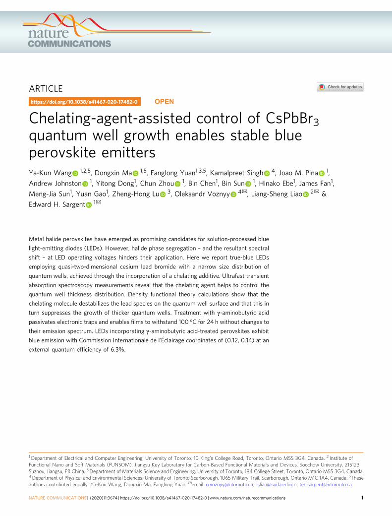
ResultsQuantum well size distribution analysis. We first examined theeffects of incorporating GABA on n QW distribution withabsorption and photoluminescence spectra (PL) measurements.Absorption of the control CsPbBr3 films—made with a precursorstoichiometry of <n>= 2 (<n> will henceforth refer to the pre-cursor stoichiometry, while n will refer to a specific QW)—exhibited an excitonic absorption peak at 425 nm, and had anemission peak at 495 nm (Fig. 1a, b). Adjusting the ligand
stoichiometry in the precursor solution to <n>= 3 redshifts theemission to around 510 nm while absorption becomes broad andfeatureless. The large Stokes shift indicates that there is a smallconcentration of larger n QWs into which created excitons arefunneled. In contrast, GABA-treated CsPbBr3 thin films of <n>= 2 and 3 both show an excitonic peak at around 450 nm andexhibit deep-blue PL emission centered at 464 and 475 nm withCIE coordinates of (0.13, 0.07) and (0.11, 0.13), respectively(Fig. 1c and Supplementary Fig. 1). This indicates that the for-mation of larger n QWs is suppressed with the inclusion ofGABA.
We sought further insight into the dynamics of photocarriersin both GABA-treated and pristine thin films. We employedfemtosecond transient absorption spectroscopy (TAS) to probethe exciton dynamics at ultrafast timescales (Fig. 1d, e). ControlCsPbBr3 thin films (<n>= 2 precursor solution) initially exhibittwo distinctive bleach peaks at 430 nm and 450 nm correspondingto n= 2 and 3 (Fig. 1d). The two bleach peaks show a slightredshift (around 2 nm), commensurate with the appearance of ann > 3 shoulder bleach peak at a longer wavelength (around 480nm) after 1 ps. <n>= 3 films show a broad bleach signal thatshifts to longer wavelengths as the delay time is increased(Fig. 1d).
In contrast, TAS for GABA-treated CsPbBr3 thin films (<n>=2) shows bleach peaks at 405, 430, and 450 nm, corresponding ton= 1, 2, 3, whose features are stable within the 100 ps timeframe(Fig. 1e). The TAS of larger CsPbBr3 QWs (<n>= 3) show nobleach peak at 405 nm, while the remaining bleach peaks aresimilar. For both <n>= 2 and <n>= 3 thin films, the GABA-treated films exhibit a narrower and more stable distributionof QWs.
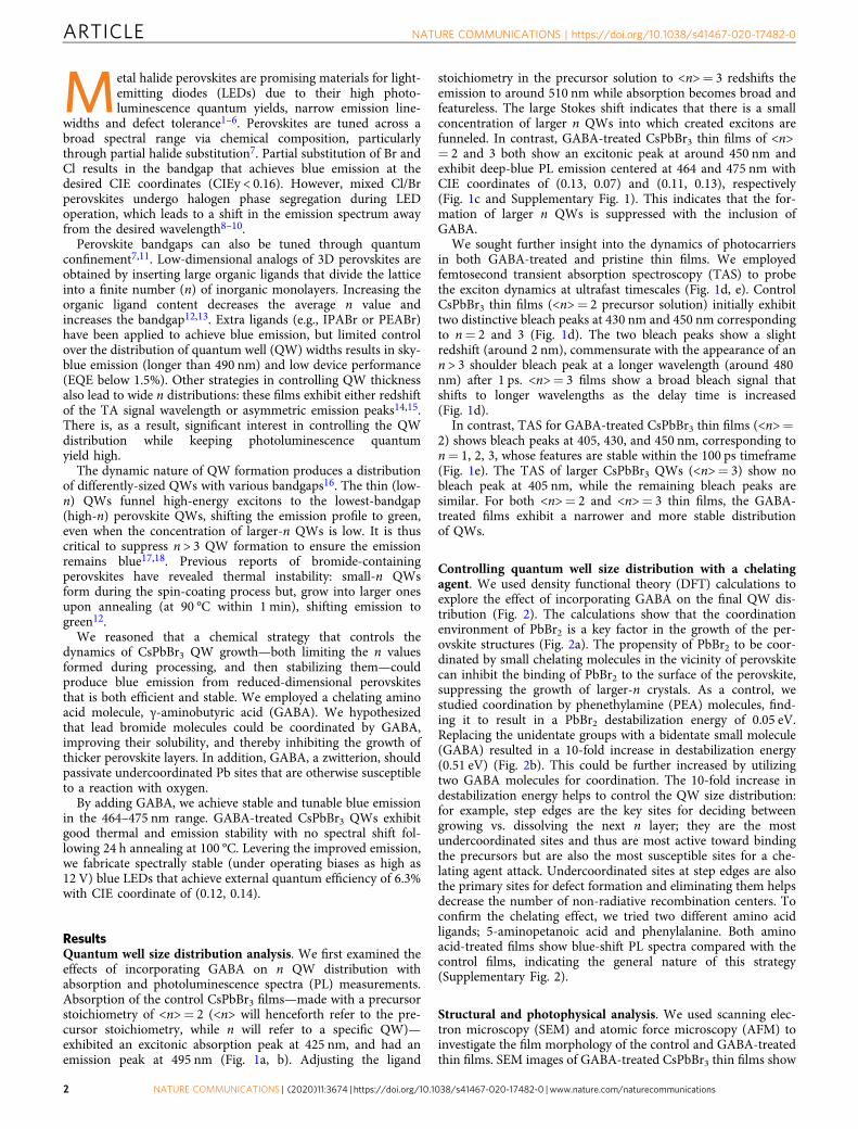
Controlling quantum well size distribution with a chelatingagent. We used density functional theory (DFT) calculations toexplore the effect of incorporating GABA on the final QW dis-tribution (Fig. 2). The calculations show that the coordinationenvironment of PbBr2 is a key factor in the growth of the per-ovskite structures (Fig. 2a). The propensity of PbBr2 to be coor-dinated by small chelating molecules in the vicinity of perovskitecan inhibit the binding of PbBr2 to the surface of the perovskite,suppressing the growth of larger-n crystals. As a control, westudied coordination by phenethylamine (PEA) molecules, find-ing it to result in a PbBr2 destabilization energy of 0.05 eV.Replacing the unidentate groups with a bidentate small molecule(GABA) resulted in a 10-fold increase in destabilization energy(0.51 eV) (Fig. 2b). This could be further increased by utilizingtwo GABA molecules for coordination. The 10-fold increase indestabilization energy helps to control the QW size distribution:for example, step edges are the key sites for deciding betweengrowing vs. dissolving the next n layer; they are the mostundercoordinated sites and thus are most active toward bindingthe precursors but are also the most susceptible sites for a che-lating agent attack. Undercoordinated sites at step edges are alsothe primary sites for defect formation and eliminating them helpsdecrease the number of non-radiative recombination centers. Toconfirm the chelating effect, we tried two different amino acidligands; 5-aminopetanoic acid and phenylalanine. Both aminoacid-treated films show blue-shift PL spectra compared with thecontrol films, indicating the general nature of this strategy(Supplementary Fig. 2).
Structural and photophysical analysis. We used scanning elec-tron microscopy (SEM) and atomic force microscopy (AFM) toinvestigate the film morphology of the control and GABA-treatedthin films. SEM images of GABA-treated CsPbBr3 thin films show
ARTICLE NATURE COMMUNICATIONS | https://doi.org/10.1038/s41467-020-17482-0
2 NATURE COMMUNICATIONS | (2020) 11:3674 | https://doi.org/10.1038/s41467-020-17482-0 | www.nature.com/naturecommunications
400 450 500 550 600
Wavelength (nm)
400 450 500 550 600
Wavelength (nm)400 450 500 550 600
Wavelength (nm)
450 500 550 600
Wavelength (nm)
–0.03
–0.02
–0.01
0
0
0.01
0.020.2 ps1 ps5 ps10 ps40 ps100 ps
0
0
a b
d
e
f
g
ΔOD
–0.03
–0.04
–0.02
–0.01
0.01
0.02
ΔOD
–0.03
–0.02
–0.02
–0.04
–0.06
–0.01
0.01
0.02
0.02
ΔOD
ΔO
D
n = 2n = 3
n > 3
n = 3
Mixture n
n = 2
n = 1
n = 2
n = 3
<n> = 2
<n> = 2
<n> = 3
<n> = 3
dynamic controlAmino-acid
H2N OH
O
γ-Aminobutyric acid
cGABA treated
400 450 500 550 600
0.0
0.5
1.0
0.0
0.5
1.0
Abs
orpt
ion
0.0
0.5
1.0
Abs
orpt
ion
Wavelength (nm)
400 450 500 550 600
Wavelength (nm)
400 450 500 550 600
Wavelength (nm)
400 450 500 550 600
Wavelength (nm)
Control
Pho
tolu
min
ance
0.0
0.5
1.0
Pho
tolu
min
ance
n = 4
n = 1
n = 3
n = 2
Photon
Photon
0.2 ps1 ps5 ps10 ps40 ps100 ps
0.2 ps1 ps5 ps10 ps40 ps100 ps
0.2 ps1 ps5 ps10 ps40 ps100 ps
Fig. 1 Photoexcited carrier dynamics of GABA-treated CsPbBr3 QWs. a Schematics depicting suppression by GABA of n < 2 and n > 3 QWs.b, c Absorption and photoluminescence spectra of the control (b) and GABA-treated (c) CsPbBr3 thin films. Inset: photograph of the perovskite films underexternal photoexcitation. d, e TAS of control (d) and GABA-treated (e) CsPbBr3 QWs with <n>= 2 and 3 at different delay times. f, g Schematics ofphotocarrier dynamics and recombination of the control (f) and GABA-treated (g) CsPbBr3 thin films.
a b
Des
tabi
lizat
ion
ener
gy (
eV)
0.0
0.8
0.4
0.2
0.6
Coordinating moleculeAA x 2 AA Control
Crystal growth
Cs
Pb
BrCNOH
Coordinationinduced
destabilization
Fig. 2 Control of 2D perovskite crystallization using a chelating agent. a Schematic of the chelating effect on PbBr2 binding to the surface. b DFT-calculated destabilization energy of PbBr2 on the surface of perovskite when coordinated with 2 GABA molecules, 1 GABA molecule, and PEA.
NATURE COMMUNICATIONS | https://doi.org/10.1038/s41467-020-17482-0 ARTICLE
NATURE COMMUNICATIONS | (2020) 11:3674 | https://doi.org/10.1038/s41467-020-17482-0 |www.nature.com/naturecommunications 3
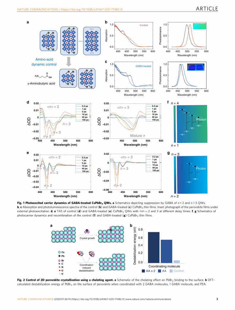
a flat and continuous film over a 2 μm area (Fig. 3a). In contrast,the control CsPbBr3 QWs shows a rougher film (Fig. 3b). Atomicforce microscopy (AFM) images of GABA-treated CsPbBr3 QWsshow a smoother morphology with an RMS of around 0.3 nm,which is much lower than that of control film (13.1 nm) (Fig. 3e,f). The better morphology of GABA-treated film is linked toimproved control of crystallization and QW size distribution, asevidenced by TAS19. Powder X-ray diffraction (PXRD) of controland GABA-treated films show typical perovskite diffraction sig-nals (Fig. 3c). Fourier transform infrared spectroscopy (FTIR)spectra of GABA-treated CsPbBr3 QWs show clear C=Oabsorption features at a 1500–1700 cm−1, which confirms that
GABA is incorporated in the films, while pristine films are fea-tureless in this range (Fig. 3d).
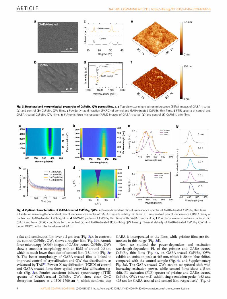
Next we studied the power-dependent and excitationwavelength-dependent PL of the pristine and GABA-treatedCsPbBr3 thin films (Fig. 4a, b). GABA-treated CsPbBr3 QWsexhibit an emission peak at 463 nm, which is 30 nm blue-shiftedcompared with the control sample (Fig. 4a and SupplementaryFig. 3a). The GABA-treated QWs exhibit no spectral shift withincreasing excitation power, while control films show a 5 nmshift. PL excitation (PLE) spectra of pristine and GABA-treatedCsPbBr3 QWs (<n>= 2) exhibit single emission peaks (463 and495 nm for GABA-treated and control film, respectively) (Fig. 4b
a ec
2 µm
2 µm
b
GABA-treated
Control
0 nm
2.5 nm
0 nm
150 nm fd
Degree (2�)
Wavenumber (cm–1)
10 20 20 µm 20 µm
20 µm 20 µm
30 40
Inte
nsity
(a.
u.)
Inte
nsity
(a.
u.)
Control
Control
NH
C=O
GABA-treated
GABA treated
1500 1600 1700 1800
Fig. 3 Structural and morphological properties of CsPbBr3 QW perovskites. a, b Top-view scanning electron microscope (SEM) images of GABA-treated(a) and control (b) CsPbBr3 QW films. c Powder X-ray diffraction (PXRD) of control and GABA-treated CsPbBr3 thin films. d FTIR spectra of control andGABA-treated CsPbBr3 QW films. e, f Atomic force microscope (AFM) images of GABA-treated (e) and control (f) CsPbBr3 thin films.
Inte
nsity
(a.
u.)
Inte
nsity
(a.
u.)
Ex
Wav
e le
ng
th (
nm
)
Inte
nsity
(a.
u.)
Time (ns)100 200 300 400
104
103
102
101
-1 -0.5 0 0.5 10
0.5
1
1.5
2
0
500
1000
1500
2000
2500
3000
3500
4000
Pristine+PEA
440 480 520 560 600
0.0
0.5
1.0
440 480 520 560 600
0.0
0.5
1.0
Wavelength (nm)
Wavelength (nm)
+BAC
GABA treated+PEA+BAC
Nor
mal
ized
inte
nsity
(a.
u.)
Wavelength (nm)400 450 500 550
5 min
1.5 h
3.0 h
5.0 h
24 hq z Å
–1)
qr Å–1)
a eb
c fd
g
n = 2 (GABA)n = 3 (GABA)n = 2 (pristine)n = 3 (pristine)
5000 3000460
450
440
430
420
410
400
2500
2000
1500
1000
500
0
–500
25
20
15
Flu
ence
(u
J cm
–2)
10
5
4000
3000
2000
1000
0
600 550 500Wavelength (nm)
450 400 600 550 500Wavelength (nm)
450 400
Fig. 4 Optical characteristics of GABA-treated CsPbBr3 QWs. a Power-dependent photoluminescence spectra of GABA-treated CsPbBr3 thin films.b Excitation wavelength-dependent photoluminescence spectra of GABA-treated CsPbBr3 thin films. c Time-resolved photoluminescence (TRPL) decay ofcontrol and GABA-treated CsPbBr3 films. d GIWAXS pattern of CsPbBr3 thin films with GABA treatment. e, f Photoluminescence features under acidic(BAC) and basic (PEA) conditions for the control (e) and GABA-treated (f) CsPbBr3 QW films. g Thermal stability of GABA-treated CsPbBr3 QW filmsunder 100 °C within the timeframe of 24 h.
ARTICLE NATURE COMMUNICATIONS | https://doi.org/10.1038/s41467-020-17482-0
4 NATURE COMMUNICATIONS | (2020) 11:3674 | https://doi.org/10.1038/s41467-020-17482-0 | www.nature.com/naturecommunications
and Supplementary Fig. 3b). This suggests that the energy transferfrom smaller to larger n QWs is efficient for both films.
Time-resolved photoluminescence (TRPL) decay of GABA-treated CsPbBr3 (<n>= 2 and 3) thin films show longer lifetimesof 13 and 15 ns, compared with 6 and 7 ns for control CsPbBr3QWs (Fig. 4c). The longer PL lifetime of GABA-treated filmssuggests its passivation effects due to the Lewis base property ofCOO− group, consistent with previous literature20. The longerlifetime of GABA-treated samples, taken with the higher PLQY(GABA-treated films of 82% and control of 40%), suggests thatGABA passivates traps and reduces the non-radiative recombina-tion rate in the films. We employed grazing-incidence wide-angleX-ray scattering (GIWAXS) to probe the orientation of thin films.The interlayer spacing between 2D perovskite layers (n= 1)is around 17 Å, and the corresponding diffraction peak is at0.37 Å−1 14. Diffraction peaks observed at smaller q values are theresult of higher (n= 2 and 3) n domains. These diffraction peaksare primarily observed as spots (instead of rings) along the qz axis.From this, we conclude that the quasi-2D perovskite layers arealigned parallel to the substrate.
Emission stability. We further investigated materials and emis-sion stability under heat/acid/base conditions of GABA-treatedCsPbBr3 films and control films. We choose benzoic acid (BAC)and phenethylamine (PEA) as acid and base sources to investigateCsPbBr3 QWs emission stability. Untreated CsPbBr3 QWs show abroadening of the emission after both treatments, suggesting thatthe QW distribution is unstable under these conditions (Fig. 4e),and consistent with DFT results that a chelating agent can dela-minate the QWs layer by layer. However, the chelating strength ofPEA and BAC is not sufficient to completely suppress n= 4layers, resulting in a broader thickness distribution. In contrast,the emission of GABA-treated CsPbBr3 QWs is largely unchan-ged after acid and base treatment, from which we conclude thatthe GABA-treated films are stable under both conditions (Fig. 4f).Similarly, GABA-treated CsPbBr3 QWs are also stable afterheating at 100 °C for 24 h (Fig. 4g).
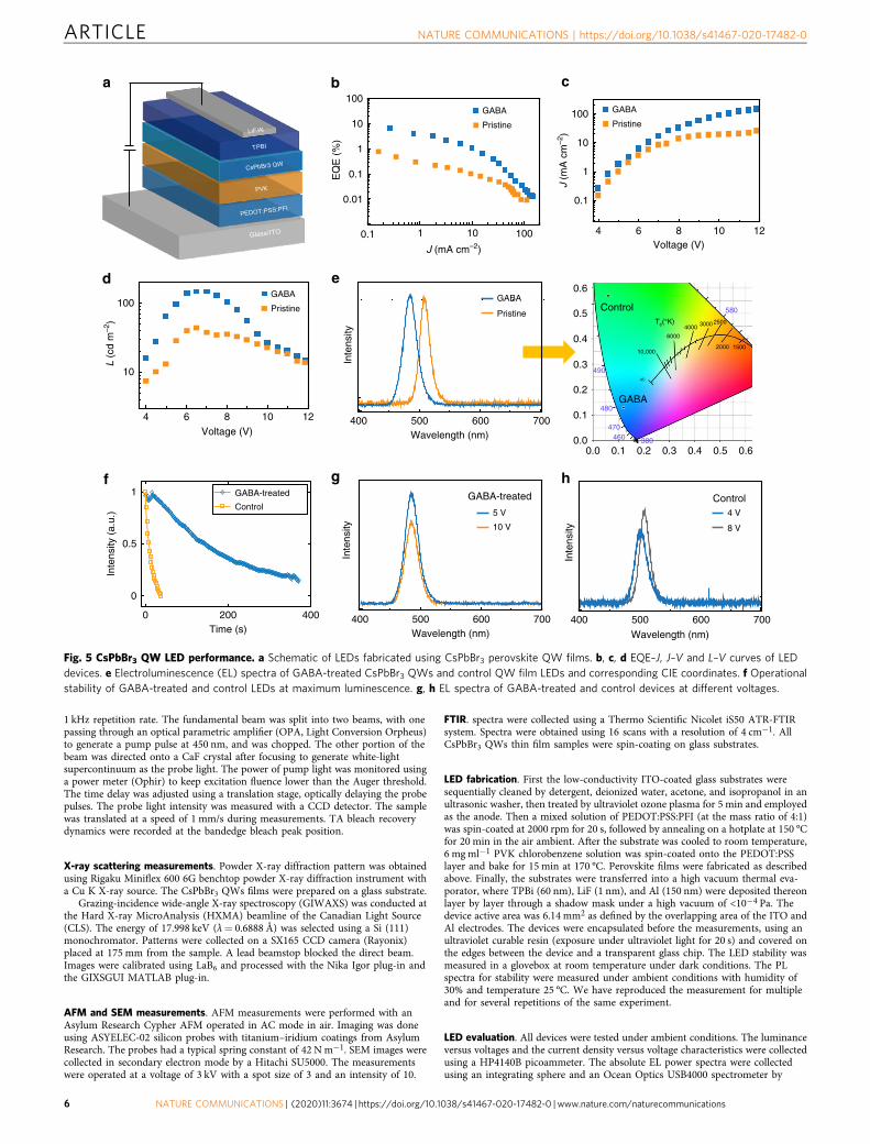
Device performance and operational stability. Levering theimproved stability and PLQYs, we incorporated the GABA-treated CsPbBr3 QWs in LEDs. We use an ITO glass substrateanode, a poly(3,4-ethylenedioxythiophene): poly(styrene-sulfo-nate) (PEDOT:PSS) mixed with Nafion hole injection layer (HIL),a poly(9-vinylcarbazole) (PVK) hole transport layer (HTL), aCsPbBr3 QW emission layer, a 1,3,5-tris(N-phenylbenzimidazol-2-yl) benzene (TPBI) electron transport layer (ETL), and a LiF/Aldouble-layered cathode, as shown in Fig. 5a and SupplementaryFig. 4. The CsPbBr3 QWs with GABA treatment exhibit true-blueemission (478 nm) with CIE coordinates of (0.12, 0.14), whereasuntreated devices emit at green wavelengths with CIE coordinatesof (0.06, 0.57) (Fig. 5e).
Luminescence (L) and current density (J) curves as a functionof voltage (V) for control and GABA-treated devices are shown inFig. 5b–d. The maximum luminescence of GABA-treated LEDs isaround 200 cd m−2, which is more than 2× higher thanthe pristine devices (Fig. 5d). The GABA-treated CsPbBr3 QWLEDs exhibit a maximum EQE of 6.3% (at 4 V, 0.26 mA, and17 cd m−2) (Fig. 5a and Supplementary Fig. 5), which is amongthe best reported blue perovskite LEDs13,17,18,21–24. We attributethe EQE and luminescence to the improved passivation ofuncoordinated Pb ions by GABA.
We investigated the device stability of GABA-treated andcontrol films under different operating conditions. The GABA-treated blue LEDs have a T50 of 150 s at 200 cd m−2, which is anorder of magnitude larger than the control device (Fig. 5f). To
determine if the improved device stability was a result of theimproved phase (and thermal) stability of the QW distribution,we check the EL spectrum under operating conditions. GABA-treated devices maintain consistent EL emission under differentvoltages (up to a bias of 12 V) and after stability tests (Fig. 5g andSupplementary Fig. 6), while the EL of the untreated films shiftedby 4 nm when the operating voltage reached to 8 V (Fig. 5h). Theimproved thermal stability of GABA-treated films inhibits thethermal degradation of the LEDs induced by device operation25.
DiscussionIn conclusion, we have demonstrated the use of chelating agentsto increase PLQY and to control CsPbBr3 QW distribution. Weincorporate γ-aminobutyric acid in the precursor solutions topassivate surfaces and destabilize the Pb sites to control thequantum well thickness distribution. Two additional amino acidligands also blue-shift PL spectra compared with control films.We fabricated a true-blue LED with CIE coordinates of (0.12,0.14) and an EQE of 6.3%. This strategy contributes in thedirection of more efficient, spectrally stable, blue LEDs.
MethodsMaterials and chemicals. Methylammonium bromide (MABr) and phenylethy-lammonium bromide (PEABr) were purchased from Dyesol. Lead bromide (PbBr2,99.998%) and cesium bromide (CsBr, 99.999%) were purchased from Alfa Aesar.Anhydrous dimethyl sulfoxide (DMSO), anhydrous chloroform, Nafion per-fluorinated resin solution (tetrafluoroethylene-perfluoro-3,6-dioxa-4-methyl-7-octenesulfonic acid copolymer, 5 wt% in a mixture of lower aliphatic alcohols andwater, containing 45% water), and lithium fluoride (LiF, >99.99%) were purchasedfrom Sigma-Aldrich. Poly(3,4-ethylenedioxythiophene)polystyrene sulfonate(PEDOT:PSS, CleviosTM PVP Al 4083) was purchased from Heraeus. 1,3,5-tris(N-phenylbenzimiazole-2-yl)benzene (TPBi) was purchased from Lumtec. All thechemicals were used directly as received.
Perovskite film fabrication. The precursor solution is prepared with equation ofPEA2Csn−1PbnBr3n+1. For GABA-treated solution, different molar ratio of GABA(0.05 and 0.1 M) is added in the precursor solution in DMSO under continuousstirring for 30 min in a nitrogen-filled glovebox at room temperature. The pre-cursor was spin-coated onto a glass substrate using a two-step method. Theresulted clear and colorless solution was dripped onto the substrates after filtration,pre-spun at 1000 rpm for 10 s, then spin-coated at 5000 rpm for 60 s. After 25 sduring the second step, 400 µL of chloroform dissolving TPPO (98%, Sigma-Aldrich) is deposited onto the perovskite film during the second step. Triphenyl-phosphine oxide (TPPO) is a passivating agent that has been reported in previousliterature26. The second step is key to the crystal growth process as this step utilizesthe antisolvent to form better film and control the perovskite growth27. Theresulting films were then annealed at 90 °C for 5 min to increase crystallization. The0.05 M for <n>= 3 is the best concentration for fabricating LEDs.
DFT calculations. Calculations were performed using the CP2K computationalpackage with the Quickstep module28. The calculations employed a grid cut-off of600 Ry, Goedecker–Teter–Hutter pseudopotentials29, Perdew–Burke–Ernzerhofexchange-correlation functional30 and MOLTOPT double-zeta plus polarizedorbital basis sets. The slabs were separated by 55 Å of vacuum in the y-directionand made periodic in the x and z direction. All geometries were relaxed until forceson atoms converged to below 40 meV Å−1. The destabilization energy was calcu-lated as the difference in energies of the structure with molecule-coordinated PbBr2and the structure with PbBr2 adsorbed on surface and non-coordinating moleculespresent within the same surface unit cell:
Edestabilization ¼ Enon�coordinated � Ecoordinated ð1Þ
Absorption, PL, PL lifetime, and PLQY measurements. Absorption spectra forCsPbBr3 QWs were collected using a fiber coupled modular spectrometer (USB2000+, ocean optics). PL spectra of CsPbBr3 QWs thin films were collected using aHoriba Fluorolog system with a xenon lamp as the excitation source. The samplewas placed at an incidence angle of 30°. The PL spectra were collected using acalibrated monochromator:single-photon-detector assembly. The PL lifetime datawas recorded on using a time-correlated single-photon counting (TCSPC) system(Horiba). PLQY is measured using an integrating sphere.
Transient absorption (TA) measurements. TA spectra were recorded using afemtosecond (fs) pump–probe spectroscopy setup. The fs laser pulses were pro-duced by a regeneratively amplified Yb:KGW laser (Light Conversion, Pharos) at
NATURE COMMUNICATIONS | https://doi.org/10.1038/s41467-020-17482-0 ARTICLE
NATURE COMMUNICATIONS | (2020) 11:3674 | https://doi.org/10.1038/s41467-020-17482-0 |www.nature.com/naturecommunications 5
1 kHz repetition rate. The fundamental beam was split into two beams, with onepassing through an optical parametric amplifier (OPA, Light Conversion Orpheus)to generate a pump pulse at 450 nm, and was chopped. The other portion of thebeam was directed onto a CaF crystal after focusing to generate white-lightsupercontinuum as the probe light. The power of pump light was monitored usinga power meter (Ophir) to keep excitation fluence lower than the Auger threshold.The time delay was adjusted using a translation stage, optically delaying the probepulses. The probe light intensity was measured with a CCD detector. The samplewas translated at a speed of 1 mm/s during measurements. TA bleach recoverydynamics were recorded at the bandedge bleach peak position.
X-ray scattering measurements. Powder X-ray diffraction pattern was obtainedusing Rigaku Miniflex 600 6G benchtop powder X-ray diffraction instrument witha Cu K X-ray source. The CsPbBr3 QWs films were prepared on a glass substrate.
Grazing-incidence wide-angle X-ray spectroscopy (GIWAXS) was conducted atthe Hard X-ray MicroAnalysis (HXMA) beamline of the Canadian Light Source(CLS). The energy of 17.998 keV (λ= 0.6888 Å) was selected using a Si (111)monochromator. Patterns were collected on a SX165 CCD camera (Rayonix)placed at 175 mm from the sample. A lead beamstop blocked the direct beam.Images were calibrated using LaB6 and processed with the Nika Igor plug-in andthe GIXSGUI MATLAB plug-in.
AFM and SEM measurements. AFM measurements were performed with anAsylum Research Cypher AFM operated in AC mode in air. Imaging was doneusing ASYELEC-02 silicon probes with titanium–iridium coatings from AsylumResearch. The probes had a typical spring constant of 42 Nm−1. SEM images werecollected in secondary electron mode by a Hitachi SU5000. The measurementswere operated at a voltage of 3 kV with a spot size of 3 and an intensity of 10.
FTIR. spectra were collected using a Thermo Scientific Nicolet iS50 ATR-FTIRsystem. Spectra were obtained using 16 scans with a resolution of 4 cm−1. AllCsPbBr3 QWs thin film samples were spin-coating on glass substrates.
LED fabrication. First the low-conductivity ITO-coated glass substrates weresequentially cleaned by detergent, deionized water, acetone, and isopropanol in anultrasonic washer, then treated by ultraviolet ozone plasma for 5 min and employedas the anode. Then a mixed solution of PEDOT:PSS:PFI (at the mass ratio of 4:1)was spin-coated at 2000 rpm for 20 s, followed by annealing on a hotplate at 150 °Cfor 20 min in the air ambient. After the substrate was cooled to room temperature,6 mgml−1 PVK chlorobenzene solution was spin-coated onto the PEDOT:PSSlayer and bake for 15 min at 170 °C. Perovskite films were fabricated as describedabove. Finally, the substrates were transferred into a high vacuum thermal eva-porator, where TPBi (60 nm), LiF (1 nm), and Al (150 nm) were deposited thereonlayer by layer through a shadow mask under a high vacuum of <10−4 Pa. Thedevice active area was 6.14 mm2 as defined by the overlapping area of the ITO andAl electrodes. The devices were encapsulated before the measurements, using anultraviolet curable resin (exposure under ultraviolet light for 20 s) and covered onthe edges between the device and a transparent glass chip. The LED stability wasmeasured in a glovebox at room temperature under dark conditions. The PLspectra for stability were measured under ambient conditions with humidity of30% and temperature 25 °C. We have reproduced the measurement for multipleand for several repetitions of the same experiment.
LED evaluation. All devices were tested under ambient conditions. The luminanceversus voltages and the current density versus voltage characteristics were collectedusing a HP4140B picoammeter. The absolute EL power spectra were collectedusing an integrating sphere and an Ocean Optics USB4000 spectrometer by
10
100GABA
Pristine
4 6 8 10 12Voltage (V)
GABA
Pristine
4 6 8 10 12
100
10
1
0.1
Voltage (V)1 10 100
100
10
1
0.1
0.01
EQ
E (
%)
GABA
Pristine
0.1
ControlTc(°K)
10,000
∞
6000
400025003000
2000 1500
GABA
0.1 0.2 0.3 0.4 0.5 0.60.0
0.1
0.2
490
580
480
470460 380
0.3
0.4
0.5
0.6
0.0
a cb
d e
f g h
J (mA cm–2)
J (m
A c
m–2
)
L (c
d m
–2)
Inte
nsity
Wavelength (nm)400 500 600 700
5 V
10 V
0 200 400Time (s)
0
0.5
1
Inte
nsity
(a.
u.)
GABA-treated
Control
Inte
nsity
Wavelength (nm)
400 500 600 700
Control4 V
8 V
400 500 600 700
Inte
nsity
Wavelength (nm)
GABA
Pristine
GABA-treated
Fig. 5 CsPbBr3 QW LED performance. a Schematic of LEDs fabricated using CsPbBr3 perovskite QW films. b, c, d EQE–J, J–V and L–V curves of LEDdevices. e Electroluminescence (EL) spectra of GABA-treated CsPbBr3 QWs and control QW film LEDs and corresponding CIE coordinates. f Operationalstability of GABA-treated and control LEDs at maximum luminescence. g, h EL spectra of GABA-treated and control devices at different voltages.
ARTICLE NATURE COMMUNICATIONS | https://doi.org/10.1038/s41467-020-17482-0
6 NATURE COMMUNICATIONS | (2020) 11:3674 | https://doi.org/10.1038/s41467-020-17482-0 | www.nature.com/naturecommunications
mounting of the devices on the wall of the integrating sphere. The EQEs were thencalculated through the measured absolute EL power spectra and the currentdensity.
Data availabilityThe data that support the findings of this study are available from the correspondingauthor upon reasonable request.
Received: 24 February 2020; Accepted: 2 July 2020;
References1. Tan, Z.-K. et al. Bright light-emitting diodes based on organometal halide
perovskite. Nat. Nanotechnol. 9, 687–692 (2014).2. Wang, J. et al. Interfacial control toward efficient and low-voltage perovskite
light-emitting diodes. Adv. Mater. 27, 2311–2316 (2015).3. Lin, K. et al. Perovskite light-emitting diodes with external quantum efficiency
exceeding 20 per cent. Nature 562, 245–248 (2018).4. MacLaughlin, C. M. Opportunities and challenges in perovskite-based display
technologies: a conversation with Andrey Rogach and Haibo Zeng. ACSEnergy Lett. 4, 977–979 (2019).
5. Chen, Q. et al. Controllable self-Induced passivation of hybrid lead iodideperovskites toward high performance solar cells. Nano. Lett. 14, 4158–4163(2014).
6. Cho, H. et al. Overcoming the electroluminescence efficiency limitations ofperovskite light-emitting diodes. Science 350, 1222–1225 (2015).
7. Protesescu, L. et al. Nanocrystals of cesium lead halide perovskites (CsPbX3, X= Cl, Br, and I): Novel optoelectronic materials showing bright emission withwide color gamut. Nano Lett. 15, 3692–3696 (2015).
8. Chiba, T. et al. Anion-exchange red perovskite quantum dots with ammoniumiodine salts for highly efficient light-emitting devices. Nat. Photonics. 12,681–687 (2018).
9. Zhang, H. et al. Phase segregation due to ion migration in all-inorganic mixed-halide perovskite nanocrystals. Nat. Commun. 10, 1088 (2019).
10. Li, G. et al. Highly efficient perovskite nanocrystal light-emitting diodesenabled by a universal crosslinking method. Adv. Mater. 28, 3528–3534(2016).
11. Tyagi, P., Arveson, S. M. & Tisdale, W. A. Colloidal organohalide perovskitenanoplatelets exhibiting quantum confinement. J. Phys. Chem. Lett. 6,1911–1916 (2015).
12. Xing, J. et al. Color-stable highly luminescent sky-blue perovskite light-emitting diodes. Nat. Commun. 9, 3541 (2018).
13. Pan, J. et al. Bidentate kigand-passivated CsPbI3 perovskite nanocrystals forstable near-unity photoluminescence quantum yield and efficient red light-emitting diodes. J. Am. Chem. Soc. 140, 562–565 (2018).
14. Jin, Y. et al. Synergistic effect of dual ligands on stable blue quasi-2Dperovskite light-emitting diodes. Adv. Funct. Mater. 30, 1908339 (2020).
15. Yantara, N. et al. Designing the perovskite structural landscape for efficientblue emission. ACS Energy Lett. 5, 1593–1600 (2020).
16. Quintero-Bermudez, R. et al. Compositional and orientational control in metalhalide perovskites of reduced dimensionality. Nat. Mater. 17, 900–907 (2018).
17. Jiang, Y. et al. Spectra stable blue perovskite light-emitting diodes. Nat.Commun. 10, 1868 (2019).
18. Liu, Y. et al. Efficient blue light-emitting diodes based on quantum-confinedbromide perovskite nanostructures. Nat. Photonics 13, 760–764 (2019).
19. Liang, Q. et al. Enhancing the crystallization and optimizing the orientation ofperovskite films via controlling nucleation dynamics. J. Mater. Chem. A 4,223–232 (2016).
20. Yang, S. et al. Tailoring passivation molecular structures for extremely smallopen-circuit voltage loss in perovskite solar cells. J. Am. Chem. Soc. 141,5781–5787 (2019).
21. Wang, Q. et al. Efficient sky-blue perovskite light-emitting diodes viaphotoluminescence enhancement. Nat. Commun. 10, 5633 (2019).
22. Hou, S. et al. Efficient blue and white perovskite light-emitting diodes viamanganese doping. Joule 2, 2421–2433 (2018).
23. Kumawat, N. K. et al. Blue perovskite light-emitting diodes: progress,challenges and future directions. Nanoscale 11, 2109–2120 (2019).
24. Li, Z. et al. Modulation of recombination zone position for quasi-two-dimensional blue perovskite light-emitting diodes with efficiency exceeding5%. Nat. Commun. 10, 1027 (2019).
25. Lee, W. et al. Ultralow thermal conductivity in all-inorganic halideperovskites. Proc. Natl Acad. Sci. USA 114, 8693–8697 (2017).
26. Quan, L. et al. Edge stabilization in reduced-dimensional perovskites. Nat.Commun. 11, 170 (2020).
27. Tavakoli, M. M. et al. Controllable perovskite crystallization via antisolventtechnique using chloride additives for highly efficient planar perovskite solarcells. Adv. Energy Mater. 9, 1803587 (2019).
28. VandeVondele, J. et al. QUICKSTEP: fast and accurate density functionalcalculations using a mixed Gaussian and plane waves approach. Comput. Phys.Commun. 167, 103–128 (2005).
29. Goedecker, S., Teter, M. & Hutter, J. Separable dual-space Gaussianpseudopotentials. Phys. Rev. B 54, 1703–1710 (1996).
30. Perdew, J. P., Burke, K. & Ernzerhof, M. Generalized gradient approximationmade simple. Phys. Rev. Lett. 77, 3865–3868 (1996).
AcknowledgementsThis work was supported by the Ontario Research Fund-Research Excellence Programand the Natural Sciences and Engineering Research Council of Canada (NSERC grantnumber 216956-12). We acknowledge financial support from Natural Science Founda-tion of China (Nos. 51821002, 91733301) and the Collaborative Innovation Center ofSuzhou Nano Science and Technology. Y.K. Wang acknowledges the financial support ofthe China Scholarship Council (No. 201806920067). Z.H.L. acknowledges the financialsupport of the National Natural Science Foundation of China (grant number 11774304).Computations were performed on the Niagara supercomputer at the SciNet HPCConsortium. SciNet is funded by the Canada Foundation for Innovation; the Govern-ment of Ontario; Ontario Research Fund - Research Excellence; and the University ofToronto.
Author contributionsE.H.S. supervised the project. E.H.S. and Y.W. wrote the paper. Y.W. conceived the study,designed the experiments. Y.W., D.M., and F.Y. fabricated the LED devices and per-formed characterization of LED devices. J.P. carried excitation and power-dependentphotoluminescence spectroscopy. Y.D. carried out the transient absorption spectroscopy.K.S. and O.V. conducted the density functional theory (DFT) calculations. A.J. per-formed GIWAXS measurements. C.Z. performed SEM imaging. J.F. performed FTIRspectroscopy measurements. B.C., B.S., H.E., Y.G., and M.S. contributed to device fab-rication and data analyses. Z.L. and L.L. helpd with discussions. All authors discussed theresults and assisted during manuscript preparation.
Competing interestsThe authors declare no competing interests.
Additional informationSupplementary information is available for this paper at https://doi.org/10.1038/s41467-020-17482-0.
Correspondence and requests for materials should be addressed to O.V., L.-S.L. or E.H.S.
Peer review information Nature Communications thanks Zhi-Kuang Tan and the other,anonymous, reviewer(s) for their contribution to the peer review of this work.
Reprints and permission information is available at http://www.nature.com/reprints
Publisher’s note Springer Nature remains neutral with regard to jurisdictional claims inpublished maps and institutional affiliations.
Open Access This article is licensed under a Creative CommonsAttribution 4.0 International License, which permits use, sharing,
adaptation, distribution and reproduction in any medium or format, as long as you giveappropriate credit to the original author(s) and the source, provide a link to the CreativeCommons license, and indicate if changes were made. The images or other third partymaterial in this article are included in the article’s Creative Commons license, unlessindicated otherwise in a credit line to the material. If material is not included in thearticle’s Creative Commons license and your intended use is not permitted by statutoryregulation or exceeds the permitted use, you will need to obtain permission directly fromthe copyright holder. To view a copy of this license, visit http://creativecommons.org/licenses/by/4.0/.
© The Author(s) 2020
NATURE COMMUNICATIONS | https://doi.org/10.1038/s41467-020-17482-0 ARTICLE
NATURE COMMUNICATIONS | (2020) 11:3674 | https://doi.org/10.1038/s41467-020-17482-0 |www.nature.com/naturecommunications 7