Embed Size (px)
Citation preview
Charge Extraction from Complex Morphologies in Bulk Heterojunctions
Michael L. Chabinyc Materials Department University of California, Santa Barbara
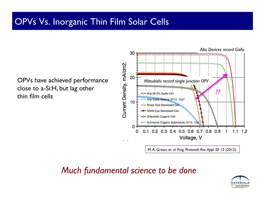
OPVs Vs. Inorganic Thin Film Solar Cells
M. A. Green, et. al. Prog. Photovolt: Res. Appl. 20 12 (2012)
Mitsubishi record single junction OPV
Alta Devices record GaAs
Much fundamental science to be done
??
OPVs have achieved performance close to a-Si:H, but lag other thin film cells

Single Phase Amorphous Semiconductors
R. A. Street Hydrogenated Amorphous Silicon (1991)
521J. Meier et al. / Thin Solid Films 451 –452 (2004) 518–524
Fig. 3. QE of the light-soaked 9.47% efficiency a-Si:H p-i-n solar cellof Figs. 2 and 4 (measurement by NREL).
Fig. 5. AM1.5 I–V characteristics of a micromorph tandem test celldeposited on glassyLP-CVD ZnO in the initial state and after 1000 hof light-exposure (1 sun at 50 8C). The mc-Si:H bottom cell has athickness of 2 mm.
Fig. 4. Light-soaking performance of the a-Si:H p-i-n cell in Figs. 2and 3. The stability experiment was performed under 1 sun AM1.5close conditions and 50 8C cell temperature. After 800 h of lightexposure the cell was sent to NREL for independent characterisation.
Fig. 6. Impact of the intermediate TCO layer on the QE of the a-Si:Htop and mc-Si:H bottom cells. The dashed lines show the tandemwithout the interlayer, the solid lines represent the one with the incor-porated intermediate TCO layer.
high open circuit voltages of 1.4 V. After the light-soaking stability test an efficiency of 10.8% could bemeasured.
3.3. Intermediate reflector in micromorph tandem cells
As already mentioned, Yamamoto et al. w9–11x havedemonstrated that the concept of an intermediate reflec-tor layer allows for an enhancement of the initial cellefficiency of micromorph tandem cells, close to 15%.IMT has observed that the intermediate layer betweenthe amorphous top and microcrystalline silicon bottomcell allows an increase in the a-Si:H top cell photocur-rent, at the cost of a reduction in the photocurrent ofthe mc-Si:H bottom cell. Nevertheless, the intermediateTCO layer allows a reduction of the top cell thicknesswhile keeping a high top photocurrent. A reduced topcell thickness, though, has the advantage of a better
stability. The impact of an intermediate TCO layer onthe QE of top and bottom cells is given in Fig. 6. Topa-Si:H cells of 0.18 mm thickness can easily achievesimilar photocurrents to top cells of 0.25 mm thicknesswithout internal TCO layers applied. However, as in ourcase, the bottom cell photocurrent is reduced. Nonethe-less, at a mc-Si:H bottom cell thickness of 2 mm short-circuit-current densities of over 11 mAycm can be2
achieved. The primary potential of this concept isimproved stability for comparable overall absorber cellthickness. Fig. 7 gives the AM1.5 I–V characteristics ofour most recent tandem cell with an intermediate TCOreflector applied leading to an initial efficiency of11.1%. The stability under light exposure of each newdevice needs to be checked; however, our fabricatedmicromorph tandems with intermediate reflectors reveala surprisingly high stable performance. As Table 1
J. Meier, et. al. Thin Solid Films 451 (2004)
Detailed study of a-Si:H revealed limits of performance and stability
Efficiency and Light Soaking
DOS

Molecular Order in Polymer:Fullerene BHJs
as-cast 90° C 120° C
150° C (010) more intense
N. D. Treat et. al. J. Mater. Chem. 21 15224 (2011)
P3HT (donor)
PCBM (acceptor)
(100)
(200)
(300)
(010)
a
Grazing Incidence X-ray Scattering of BHJ
GIWAXS of crystalline PCBM
Domain sizes small and significant disorder in both phases

Free
Ene
rgy
ground state
D + A
Charge Formation in Bulk Heterojunctions
D+ : A-
proximal carriers (~2 nm)
(D+ A-)
charge transfer electronic state
charge formation
Distance
free carriers
D+ + A-
free carriers ( > ~10 nm)
~ [I.E.(D)-E.A.(A)]
bulk heterojunction
exciton
D* + A
photon
excited state
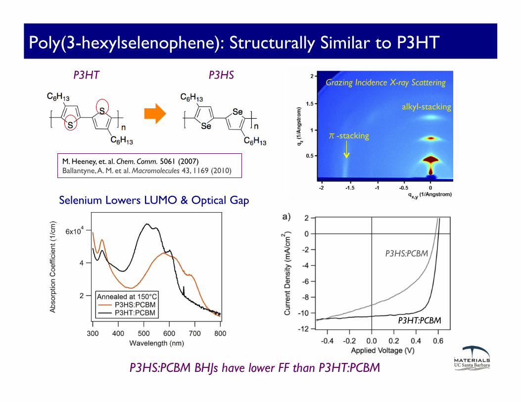
Poly(3-hexylselenophene): Structurally Similar to P3HT
Grazing Incidence X-ray Scattering
π-stacking
alkyl-stacking
Selenium Lowers LUMO & Optical Gap
P3HS:PCBM BHJs have lower FF than P3HT:PCBM
P3HT:PCBM
P3HS:PCBM
P3HS P3HT
M. Heeney, et. al. Chem. Comm. 5061 (2007) Ballantyne, A. M. et al. Macromolecules 43, 1169 (2010)

Fabricate pure bilayer Fullerene-polymer miscibility increases with temperature
P3HS-fullerene Miscibility Increases with Temperature
P3HS:fullerene
Fullerene
N. Treat, C. Takacs, et. al J. Am. Chem. Soc. http://dx.doi.org/10.1021/ja305875u
1,4-Fullerne Adducts
• PCBM is ~60% more miscible in P3HS than P3HT • Decreasing side chain length in1,4-adducts decreases miscibility
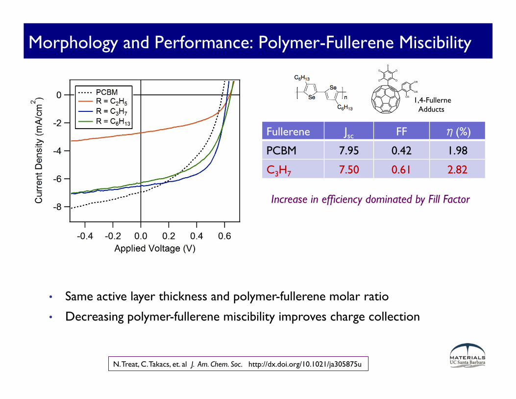
Morphology and Performance: Polymer-Fullerene Miscibility
• Same active layer thickness and polymer-fullerene molar ratio
• Decreasing polymer-fullerene miscibility improves charge collection
N. Treat, C. Takacs, et. al J. Am. Chem. Soc. http://dx.doi.org/10.1021/ja305875u
Fullerene Jsc FF η(%)
PCBM 7.95 0.42 1.98
C3H7 7.50 0.61 2.82
Increase in efficiency dominated by Fill Factor
1,4-Fullerne Adducts
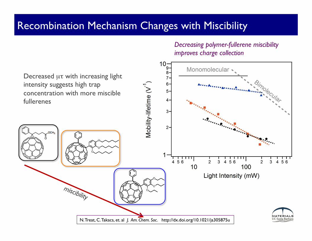
Recombination Mechanism Changes with Miscibility
Decreasing polymer-fullerene miscibility improves charge collection
Decreased µτ with increasing light intensity suggests high trap concentration with more miscible fullerenes
N. Treat, C. Takacs, et. al J. Am. Chem. Soc. http://dx.doi.org/10.1021/ja305875u
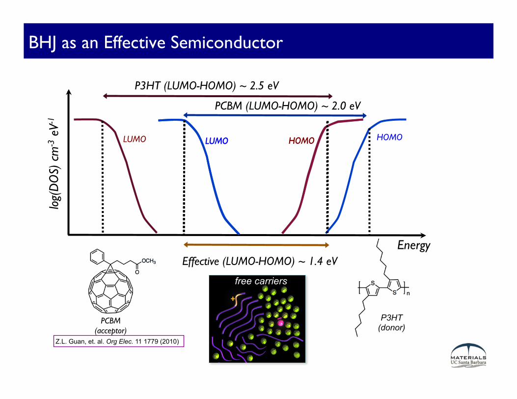
BHJ as an Effective Semiconductor
Energy
log(
DO
S) c
m-3 e
V-1
P3HT (donor)
Z.L. Guan, et. al. Org Elec. 11 1779 (2010)
PCBM (acceptor)
P3HT (LUMO-HOMO) ~ 2.5 eV
HOMO LUMO
PCBM (LUMO-HOMO) ~ 2.0 eV
LUMO HOMO
Effective (LUMO-HOMO) ~ 1.4 eV
HOMO LUMO
free carriers

Charge Transfer States Reveal Effective Gap
Significant recent progress in understanding tail of EQE revealing CT-states, disorder and minimum gap
a strong band gap absorption, which tails into the gap at lowenergies. The generated spectra are in accordance with thetheoretically8 and experimentally9 established picture of thedensity of states !DOS" distribution in disordered organicsemiconductors, describing the valence and conduction bandas being Gaussian shaped and broadened to generate an ex-ponential tail of states extending into the gap, in whichcharge carriers can be effectively trapped. Intermixing thesecompounds yields quite a different picture, with a more pro-nounced absorption tail. It is clear that mixing extends theexponential tail of valence and/or conduction band of one orboth constituting semiconductors deeper into the gap, yield-ing a more complex DOS distribution. To get more precisedata concerning this spectral region and to increase the ex-perimental relevance for solar cell research, a series of FTPSmeasurements were performed directly on solar cells.
FTPS spectra of solar cells with an active layer ofMDMO-PPV containing a PCBM percentage by weightranging from 70, 80–90 wt% are displayed in Fig. 2!a". Theabsorption peak at 2.30 eV can be assigned to the !!!*
transition in MDMO-PPV. The distinct peak at 1.77 eV isdue to the forbidden highest occupied molecular orbital-lowest unoccupied molecular orbital transition in PCBM.10
As expected, the absorption peak at 1.77 eV is more pro-nounced with increasing PCBM content. A broad spectralresponse was measured below the band gap of both semicon-ductors, similar to the obtained PDS data. This spectral re-gion is divided into two parts: !i" part E tentatively assignedto an exponential absorption tail !ii" part D tentatively as-signed to the defect absorption. Varying the composition ofthe active layer induces a change in the exponential distribu-tion of states, which could be related to the difference indisorder in the respective films. All the same, the defect ab-sorption increases with the PCBM content. To investigatewhether the absorption data in regions E and D reflect opticaltransitions due to structural defects, the cell was subjected toa sequence of “degradation” steps, involving a stepwise ex-
posure to UV light. After every step the FTPS spectrum wasrecorded and the open-circuit voltage !Voc" measured underthe low power illumination conditions of the spectrometer#Fig. 2!b"$. The absorption in region D is enhanced duringthe first series of steps !5 min". When subjecting the solarcell to longer exposure times !1 h", the absorption is stronglyincreased and has the tendency to saturate, while the E partstays unaltered. The Voc decreased in every step and stabi-lized after 1 h, 15 min of degradation. This indicates the cre-ation of !structural" defects, an intrinsic material property,rather than a difference in composition as erroneously couldbe concluded from Fig. 2!a".
More insight into the effect of film morphology on thespectral photocurrent response was provided by FTPS mea-surements on P3HT:PCBM !66%" solar cells. In Fig. 3!a",the spectrum of nonannealed and annealed cell !80 °C,5 min" is displayed. Two major effects are observed: !i" anincrease of spectral response by one order of magnitudearound 2 eV and !ii" a spectral shift of the exponential tail ofseveral tenths of meV to lower energy. The first effect is dueto a reestablishment of the ordering in the P3HT chain,which was lost during spin coating of the polymer in a com-posite film with PCBM.6 This spectral shift is accompaniedby a fourfold increase of the cell’s short circuit current, mea-sured under AM 1.5 illumination. The second effect can beexplained in terms of an exponential tail of states extendingdeeper into the gap when the cell is exposed to an annealingprocedure. This effect was investigated further, focusing onthe spectral region in question, applying a stepwise annealingprocedure !5 min" on a nonannealed cell #Fig. 3!b"$. A spec-tral shift towards lower energies is observed until a tempera-ture of 150 °C is reached. This effect can be a result of thedenser packing between the P3HT chains. Annealing the cellat 175 °C invokes an opposite shift, a possible consequenceof the deterioration of the packing at higher temperatures. It
FIG. 1. !a": PDS-spectrum of dropcast layers of MDMO-PPV !square",PCBM !star" and MDMO-PPV:PCBM !80 wt% " !pentagon". !b": PDS spec-tra of dropcast layers of P3HT !square", PCBM !star" and P3HT:PCBM!66.66 wt% " !pentagon". The full symbols !PCBM=star" correspond to dataobtained with transmittance and reflectance measurements.
FIG. 2. !a": FTPS spectrum of solar cells with an active layer of MDMO-PPV:PCBM !70% by weight" !full line", MDMO-PPV:PCBM !80% byweight" !dashed line", MDMO-PPV:PCBM !90% by weight" !dotted line".Figure 2!b": evolution of the absorption in the D region of MDMO-PPV:PCBM !80% by weight" with increasing exposure to UV illumination,fresh !square", 5 min !circle", 10 min !up triangle", 15 min !down triangle",1 h, 15 min !diamond", 2 h, 15 min !hexagon", 3 h, 15 min !star".
052113-2 Goris et al. Appl. Phys. Lett. 88, 052113 !2006"
L. Goris, et. al. Appl. Phys. Lett. 88 052113 (2006)
new states in BHJ
R. Street, et. al Phys. Rev. B.. 83, 165207 (2011)
Schematic of DOS of BHJ
tail states

Impact of Density Electronic States
• Origin of Voc - tail states and recombination mechanism •Operation at range of illumination - e.g. indoor to outdoor applications
Carrier density in OPVs is low; tail states are critical to operation
What about extrinsic states , i.e. impurities & degradation?
Energy lo
g(D
OS)
cm
-3 e
V-1 h+ e-

Chemical Nature of Electronic Traps
H. T. Nicolai, et. al. Nat. Mater. DOI: 10.1038/NMAT3384 (2012)
Water as an electron trap?
Street, Northrup, Krusor Phys. Rev. B. 85 205211 (2012)
Hydrogen induced defects?
2274
www.advmat.dewww.MaterialsViews.com
wileyonlinelibrary.com © 2012 WILEY-VCH Verlag GmbH & Co. KGaA, Weinheim
COM
MUN
ICATI
ON
Adv. Mater. 2012, 24, 2273–2277
with added PC 84 BM at concentrations (by weight with respect to PC 60 BM) of 0.1%, 1%, and 5%.
In agreement with earlier observations for polythiophene:fullerene composite, [ 14 ] the initial decay of the photocurrents which occurs during a time span on the order of
100 ps following pulsed excitation results from carrier localiza-tion at traps rather than carrier annihilation via recombination. This conclusion is supported by the demonstration of internal quantum effi ciency (IQE) in PCDTBT:PC 60 BM-based solar cells approaching 100%. [ 2 ]
The rate of carrier localization exhibited in Figure 1 for BHJ fi lms with added PC 84 BM impurities is higher compared that in the pristine PCDTBT:PC 60 BM fi lm, indicating that within a time comparable to the measuring system temporal resolu-tion ( ! 100 ps) the photoexcited electrons are localized at the PC 84 BM traps.
Figure 2 displays the transient photocurrent waveforms measured at various temperatures for pristine PCDTBT:PC 60 BM fi lm and for fi lm with 1% added concentration of PC 84 BM (by weight percent with respect to the PC 60 BM). The detailed data depicting various added concentration of PC 84 BM (0.1%–5%) are included in the Supporting Information (Figure S1). The data clearly exhibit a strong dependence on temperature of the photocurrent in the nanosecond time regime. The present data analysis indeed reveals thermally activated behavior in this time regime and yields the magnitude and time-dependence of the activation energy. We focus on delay times greater than 500 ps in order to examine the transport following the initial car-rier localization. Each of the measured transient photocurrent waveforms shown in Figure 2 was fi rst fi tted to a tri-exponen-tial function in order to reduce error due to photocurrent data fl uctuations. The Arrhenius plots of the fi tted photocurrent vs.
Scheme 1 . Schematic representation of the HOMO and LUMO level alignment of PCDTBT, PC 60 BM ( E LUMO = 4.3 eV), and PC 84 BM ( E LUMO = 4.65 eV), the profi le of the localizing states introduced by the PC 84 BM molecules, as well as the various excitation routes and hopping: (A) The transport of carriers occupying states near the HOMO and LUMO characterized by higher mobility, (B) Relaxation of carriers into progressively deeper localizing states, (C) Hopping of carriers within a band of localized states created by the PC 84 BM impurities, and (D) Carrier hopping between a localized state and states near the HOMO and LUMO characterized by higher mobility.
Figure 1 . Normalised transient photocurrent waveforms measured in a pristine PCDTBT:PC 60 BM composite fi lm and in fi lms prepared with added concentration of 0.1%, 1% and 5% of PC 84 BM with respect to the PC 60 BM in the pristine composite at room temperature.
0.0 1.0x10⁻⁹ 2.0x10⁻⁹ 3.0x10⁻⁹
0.0
0.5
1.0
Control 0.1wt% 1wt% 5wt%
Cur
rent
(a.u
.)
Time (s)
Intentional introduction of traps
Leong, et. al. Adv. Mater. 24 2273 (2012)
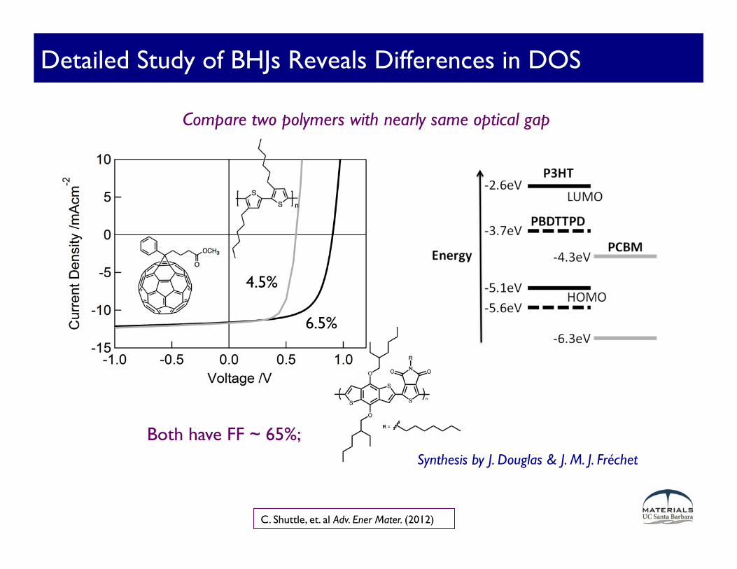
Detailed Study of BHJs Reveals Differences in DOS
6.5%
4.5%
Both have FF ~ 65%;
Compare two polymers with nearly same optical gap
Synthesis by J. Douglas & J. M. J. Fréchet
C. Shuttle, et. al Adv. Ener Mater. (2012)

Transient Measurements Reveal Dynamics (and Energetics)
Transient measurements probe the electronic density of states through transport and recombination
Charge Extraction in a Linearly Increasing Voltage CELIV
Charge Extraction or Sweep Out or Transient Photoconductivity
Transient Photovoltage
A. J. Mozer, et. al. Phys. Rev. B. 72 035217 (2005)
R. Street, et. al. Phys. Rev. B. 84 075208 (2011)
C. G. Shuttle, et. al. Appl. Phys. Lett.. 92 093311 (2008)

Charge Extraction from BHJ Photovoltaics
R. Street, et. al. Phys. Rev. B. 84 075208 (2011) C. Shuttle, et. al Adv. Ener. Mater. 2 111-119 (2012)
Transient photoconductivity provides timescale of transport and thereby energetics of electronic states
time
light
current
Charges travel to the electrode in dark and have the chance to
recombine
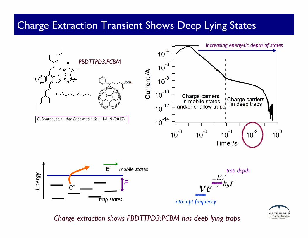
Charge Extraction Transient Shows Deep Lying States
e- Ener
gy mobile states
trap states
e-
E νe−E kbT
trap depth
attempt frequency
Increasing energetic depth of states
C. Shuttle, et. al Adv. Ener. Mater.. 2 111-119 (2012)
Charge extraction shows PBDTTPD3:PCBM has deep lying traps
PBDTTPD3:PCBM

Charge Extraction from BHJ Photovoltaics
PBDTTPD3 Increasing energetic depth of states
- possible that there are no deep states (unlikely)
No deep states observed for P3HT! C. Shuttle, et. al Adv. Ener. Mater.. 2 111-119 (2012)
P3HT
- most likely cause: doping of P3HT requires carrier concentration ~1015 cm-3 (confirmed by ESR)
HOMO ~ 5.6 eV HOMO ~ 5.1 eV

Can We Learn More from Transients?
Fit to combination of transient photocurrent measurements and steady state data
Downside: numerical simulation with many parameters must be very careful to vary measurements and fit all data self-consistently
Use 1-D model to examine transport, i.e. reduce BHJ to an amorphous semiconductor
R. MacKenzie, et. al. Adv. Ener. Mater. (2012)
1) Solve Poisson Equation 2) Recombination by Shockley-Reed-Hall
mechanism
3
COM
MUN
ICATIO
N
www.MaterialsViews.comwww.advenergymat.de
© 2012 WILEY-VCH Verlag GmbH & Co. KGaA, Weinheim wileyonlinelibrary.com
FULL PA
PER
holes. [ 23 ] A diagram of the DoS, trapping, de-trapping, and recombination model is given in Figure 1 . It can be seen that for the trapped carriers we have assumed an exponential DoS and for the free carriers we have assumed a parabolic band. We include 80 electron trap levels and 80 hole trap levels each of width 10 meV between the HOMO and LUMO. Considering one electron trap (Figure 1 ), the electron density ( n t ) of this trap is given by the rate equation;
!nt
!t= rec ! ree ! rhc + rhe
(6) where the rate r ec is the rate at which free electrons get trapped, r ee is the rate which electrons can escape from the trap back to the free electron population, r hc is the rate at which free holes get trapped and r he is the rate at which holes escape back to the free hole population. Thus recombination for an electron trap is defi ned as a free hole annihilating a trapped electron. The same equation can be written for a hole trap, in which case recombination would be defi ned as a free electron annihilating a trapped hole. The rates as derived by detailed balance are given in Table 1 . [ 24 ] The carrier escape rates for electrons and holes are given by
en = vth!n Ncex p
!E t ! E c
kT
"
(7)
and
ep = vth!p Nvex p
!E v ! E t
kT
"
(8)
respectively, where v th is the thermal emission velocity of the carriers, ! n,p are the trap cross sections and N c,v are the effec-tive density of states for free carriers. Thus, the energetically deeper a trap is, the harder it is for a carrier to escape. For the fi rst modeling exersise, the DoS of the trap states is defi ned as the exponential
"e /h(E ) = Ne /hex p(E /E e /h
u ) (9)
where E e/hU is characteristic tail slope energy and N e/h is the
magnitude of the trap DoS at the LUMO or HOMO band edge respectively. The value of N t (see Table 1 ) for a single trap is obtained by averaging the DoS function in equation 9 over the energy range " E assigned to that trap:
Nt(E ) =
# E + "E / 2E !"E/2 " e(E )d E
"E.
(10)
The electron recombination rate ( R e ) in equation 2 can then
be calculated by subtracting the total number of electrons which escape all traps into the carrier free electron population from the total number of electrons captured from the free car-rier population into all traps. An analogous procedure is carried out to calculate R h for free holes.
3. Electrical Measurements A P3HT:PCBM device was studied to provide data for the model. The device showed a short circuit current density of 11.4 mA cm # 2 , an open circuit voltage of 0.6 V, a fi ll factor of 0.64 and an effi ciency of 4.48% under simulated Air Mass 1.5 irradation. The fabrication of this device is described in the Supporting Information. Four different measurement tech-niques were employed to characterize the device: J – V measure-ments, charge-extraction measurements, transient photocurrent measurements, and transient photovoltage measurements. Both J – V and charge-extraction measurements are described elsewhere. [ 6 ]
Table 1. Shockley–Read–Hall trap capture and emission rates, where N t is the trap density of a single carrier trap and f is the fermi-Dirac occupa-tion function. [ 24 ]
Mechanism Label Description
Electron capture rate r ec nv th ! n N t (1 # f )
Electron escape rate r ee e n N t f
Hole capture rate r hc pv th ! p N t f
Hole escape rate r he e p N t (1 # f )
Figure 1 . A diagram of the density of states used in the model. The elec-tron/hole capture and escape processes are shown for a single electron trap, analogous processes happen for all electron and hole traps.
Adv. Energy Mater. 2012,DOI: 10.1002/aenm.201100709

Simulation Reveals Complex Density of States
free carriers
No reason to believe simple exponential or Gaussian is adequate to describe electronic landscape
Disorder in BHJ blends leads to distribution of electronic states P3HT:PCBM
Drift-Diffusion Model w/ SRH trapping
R. MacKenzie, et. al Adv. Ener. Mater. (2012)
Electron States
Hole States

Morphology?: Dynamics-based Methods Molecular level simulation
Simulated transport data
For > 1D model, either coarse morphologies are chosen or “molecular” level detail from simulation
In both cases, still difficult to understand molecular electronic coupling and electric DOS Simulation of morphology of BHJs with two (or more!) materials particularly difficult
J. J. Kwiatkowski, et. al. Phys. Chem. Chem. Phys. 10 1852 (2008)

Novel Approaches to Simulating Morphology
K. Delaney, H. Ceniceros, G. Fredrickson (UCSB)

Well Ordered Semiconducting Block Copolymers
Exciton diffusion length S.-Y. Ku, M. A. Brady, et. al. J. Am. Chem. Soc. DOI: 10.1021/ja307431k
Block Co-polymer Synthesis
[010]
[100]
Resonant Soft X-ray Scattering
AFM
200 nm
Model systems critical to understand models of operation and theory

Next Steps in Fundamental Science of BHJs
Transport and Device Physics - experimental methodologies to study energetics of states - transport models that capture essential physics with morphology - nature of defect states
Materials - structurally controlled BHJs
Impact: ultimate limits of performance and stability of OPVs and fundamental science of complex disordered materials


![Morphologies and separation characteristics of ... · degumming of vegetable oil [10], reuse of extraction solvent in the food industry [11] and purification of pharmaceutically active](https://img.pdfslide.us/doc/110x75/5e996f75ee9e7e093d596599/morphologies-and-separation-characteristics-of-degumming-of-vegetable-oil-10.jpg)