Embed Size (px)
Citation preview

This content has been downloaded from IOPscience. Please scroll down to see the full text.
Download details:
IP Address: 150.29.197.24
This content was downloaded on 02/06/2016 at 09:14
Please note that terms and conditions apply.
Characterization of Ultrathin Fe–Co Layer Grown on Amorphous Co–Fe–B by In situ
Reflective High-Energy Electron Diffraction
View the table of contents for this issue, or go to the journal homepage for more
2013 Appl. Phys. Express 6 063003
(http://iopscience.iop.org/1882-0786/6/6/063003)
Home Search Collections Journals About Contact us My IOPscience
Characterization of Ultrathin Fe–Co Layer Grown on Amorphous Co–Fe–B
by In situ Reflective High-Energy Electron Diffraction
Hiroyuki Hosoya1;3, Yoshinori Nagamine1;3, Koji Tsunekawa1;3, Vadym Zayets2, and Shinji Yuasa2;3�
1Process Development Center, Canon ANELVA Corporation, Kawasaki 215-8550, Japan2National Institute of Advanced Industrial Science and Technology (AIST), Spintronics Research Center, Tsukuba, Ibaraki 305-8568, Japan3CREST, Japan Science and Technology Agency (JST), Kawaguchi, Saitama 332-0012, Japan
E-mail: [email protected]
Received April 8, 2013; accepted May 8, 2013; published online May 23, 2013
The textured MgO(001) tunnel barrier grown on CoFeB is a fundamental building block for spintronic devices such as magnetic tunnel junctions.
Although the insertion of an ultrathin Fe–Co layer between an MgO layer and a bottom CoFeB layer is a common technique for improving the
magnetoresistance effect, the characteristics of this technique remain unclear. We systematically investigated the as-grown structure of Fe–Co by
reflective high-energy electron diffraction and found that a highly textured MgO(001) is formed only on an amorphous Fe–Co surface. The
diffusion of B atoms from underlying CoFeB into Fe–Co is what makes the as-grown Fe–Co layer amorphous.
# 2013 The Japan Society of Applied Physics
MgO-based magnetic tunnel junctions (MTJs) with a(001)-oriented single-crystalline or polycrystalline(textured) MgO tunnel barrier exhibit a giant
tunnel magnetoresistance (TMR) effect with magnetoresis-tance (MR) ratios of up to a few hundred percent at roomtemperature (RT).1–3) MTJs with a CoFeB/MgO/CoFeBstructure are especially useful for practical applicationssuch as magnetic sensors and spin-transfer-torque mag-netoresistive random access memory (STT-MRAM) due totheir compatibility with mass-manufacturing processes.4) InCoFeB/MgO/CoFeB MTJs, the CoFeB bottom electrodelayer is first formed as an amorphous phase and then atextured MgO(001) barrier layer is grown on the amorphousCoFeB surface at room temperature, usually by sputteringdeposition. By post-annealing the CoFeB/MgO/CoFeBstructure, the CoFeB electrode layers can be crystallizedfrom the interfaces with the MgO(001) layer due to solid-phase epitaxial growth.5,6) As a result, the MTJ struc-ture becomes textured bcc CoFeB(001)/MgO(001)/bccCoFeB(001), which is essential for the giant MR ratios.
The basic CoFeB/MgO/CoFeB structure is often mod-ified, for example, by inserting an ultrathin Fe–Co layerbetween the MgO and CoFeB layers to further optimize themagneto-transport properties.7–10) In our previous study,8)
we fabricated perpendicularly magnetized MTJs with thebottom electrode structure of CoPt/Co60Fe20B20 (1 nm)/Fe30Co70 (0.3 nm). Without the 0.3-nm-thick insertion layer,we observed a significant reduction in the MR ratio.Schreiber et al.9) observed an increase in the MR ratio from105 to 192% by inserting a 1.5-nm-thick Fe10Co90 layerbetween the bottom CoFeB electrode and MgO barrierlayers. Yoshida et al.10) observed a similar increase inthe MR ratio by inserting a 0.4-nm-thick Fe50Co50 layerbetween the bottom CoFeB electrode and MgO barrierlayers. The insertion of an ultrathin Fe–Co layer oftenimproves the MR ratio, especially in an ultralow resistance–area (RA) product region and/or when the post-annealingtemperature is relatively low (�250 �C) although thedetailed mechanism has been unclear. Note that the highMR ratio with ultra-low RA product is important for bothhigh-density STT-MRAM and read heads of hard disk drives(HDDs), and the low annealing temperature is important forthe HDD read heads, whose process temperature should bekept below about 250 �C.
To investigate the mechanism of the MR enhancement,Choi et al.7) investigated the growth and crystallizationprocesses of the CoFeB/Fe–Co/MgO structure by cross-sectional transmission electron microscopy (TEM) andconcluded that the Fe–Co layer deposited on an amorphousCoFeB crystallizes in the bcc(001) textured structure inthe as-grown state and acts as a template to crystallize theMgO layer in a highly (001)-oriented texture. This claimis, however, contradictory to previous works reporting thata highly oriented MgO(001) layer can be grown on anamorphous CoFeB surface.4–6) Although the insertion of anultrathin Fe–Co layer is a commonly used technique both inbasic research and device application, there have been nosystematic reports on the structure and functions of theinsertion layer. In this study, we systematically investigatedthe growth and crystallization processes of the CoFeB/Fe–Co/MgO structure by in situ reflective electron diffraction(RHEED) and obtained a phase diagram of the as-grownFe–Co layer with respect to the thickness and chemicalcomposition. We also investigated the diffusion of B atomsfrom the underlying CoFeB into the Fe–Co layer.
The thin films were deposited on thermally oxidizedSi(001) wafers of 200mm diameter using a magnetron-sputtering system (Canon ANELVA C-7100) developedfor the mass production of HDD read heads and MRAM.The stacking structure of the samples is shown in Fig. 1. Weused standard techniques and conditions for preparing theCoFeB/MgO/CoFeB MTJ films4,11–13) and deposited a 30-�A-thick Co60Fe20B20 layer that corresponds to the bottomferromagnetic electrode of MTJ onto a thermally oxidizedSi substrate with a Ta seed layer. On the CoFeB layer,we deposited a Fe–Co alloy layer with various thicknesses(0 to 30 �A) and chemical compositions (from Fe90Co10 toFe10Co90) at RT. Then, a 10- �A-thick MgO layer, whichcorresponds to the tunnel barrier of the MTJ, was depositedat RT by rf sputtering from an MgO target under practicalconditions for achieving giant MR ratios.12) We performedin situ RHEED observation to characterize the structureof each layer (see Fig. 1). A special RHEED observationchamber was attached to our manufacturing-type sputteringsystem for the in situ RHEED observations. In situ RHEEDis an ideal technique to observe the as-grown surfacestructure of ultrathin layers. Note that in the cross-sectionalTEM observations, the processes to prepare the TEM
Applied Physics Express 6 (2013) 063003
063003-1 # 2013 The Japan Society of Applied Physics
http://dx.doi.org/10.7567/APEX.6.063003
samples (ion milling, etc.) might damage the samples andchange the structure from the as-grown one.
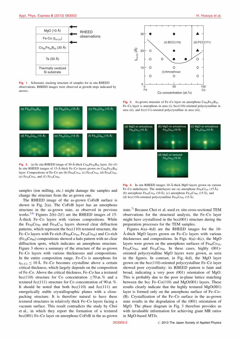
The RHEED image of the as-grown CoFeB surface isshown in Fig. 2(a). The CoFeB layer has an amorphousstructure in the as-grown state, as observed in previousworks.5,6) Figures 2(b)–2(f ) are the RHEED images of 15-�A-thick Fe–Co layers with various compositions. Whilethe Fe50Co50 and Fe30C70 layers showed clear diffractionpatterns, which represent the bcc(110) textured structure, theFe–Co layers with Fe-rich (Fe90Co10, Fe70Co30) and Co-rich(Fe10Co90) compositions showed a halo pattern with no cleardiffraction spots, which indicates an amorphous structure.Figure 3 shows a summary of the structure of the as-grownFe–Co layers with various thicknesses and compositions.In the entire composition range, Fe–Co is amorphous fortFe{Co � 10 �A. Fe–Co becomes crystalline above a certaincritical thickness, which largely depends on the compositionof Fe–Co. Above the critical thickness, Fe–Co has a texturedbcc(110) structure for Co concentration �70 at.% and atextured fcc(111) structure for Co concentration of 90 at.%.It should be noted that both bcc(110) and fcc(111) areenergetically stable crystallographic planes with a close-packing structure. It is therefore natural to have thesetextured structures in relatively thick Fe–Co layers facing avacuum surface. This result contradicts the study by Choiet al., in which they report the formation of a texturedbcc(001) Fe–Co layer on amorphous CoFeB in the as-grown
state.7) Because Choi et al. used ex situ cross-sectional TEMobservations for the structural analysis, the Fe–Co layermight have crystallized in the bcc(001) structure during thepreparation processes for the TEM samples.
Figures 4(a)–4(d) are the RHEED images for the 10-�A-thick MgO layers grown on Fe–Co layers with variousthicknesses and compositions. In Figs. 4(a)–4(c), the MgOlayers were grown on the amorphous surfaces of Fe90Co10,Fe50Co50, and Fe10Co90. In these cases, highly (001)-oriented polycrystalline MgO layers were grown, as seenin the figures. In contrast, in Fig. 4(d), the MgO layergrown on the bcc(110)-oriented polycrystalline Fe–Co layershowed poor crystallinity: its RHEED pattern is faint andbroad, indicating a very poor (001) orientation of MgO.This is probably due to the poor in-plane lattice matchingbetween the bcc Fe–Co(110) and MgO(001) layers. Theseresults clearly indicate that the highly textured MgO(001)layer is formed only on the amorphous surface of Fe–Co–(B). Crystallization of the Fe–Co surface in the as-grownstate results in the degradation of the (001) orientation ofMgO. The phase diagram in Fig. 3 therefore provides uswith invaluable information for achieving giant MR ratiosin MgO-based MTJs.
(b) Fe90Co10 (15 Å) (c) Fe70Co30 (15 Å)
(d) Fe50Co50 (15 Å) (e) Fe30Co70 (15 Å) (f) Fe10Co90 (15 Å)
(a) Fe20Co60B20
Fig. 2. (a) In situ RHEED image of 30- �A-thick Co60Fe20B20 layer. (b)–(f)
In situ RHEED images of 15- �A-thick Fe–Co layers grown on Co60Fe20B20
layer. Compositions of Fe–Co are (b) Fe90Co10, (c) Fe70Co30, (d) Fe50Co50,
(e) Fe30Co70, and (f) Fe10Co90.
0 50 100
Co concentration (at.%)
t Fe-
Co
(Å)
Fe Co
0
10
20
30
(i) Amorphous
(ii) BCC(110) (iii) FCC(111)
Fig. 3. As-grown structure of Fe–Co layer on amorphous Co60Fe20B20.
Fe–Co layer is amorphous in area (i), bcc(110)-oriented polycrystalline in
area (ii), and fcc(111)-oriented polycrystalline in area (iii).
Fe-Co (tFe-Co)
Co60Fe20B20 (30 Å)
Ta (50 Å)
Thermally oxidized Si substrate
MgO (10 Å) RHEEDobservations
Fig. 1. Schematic stacking structure of samples for in situ RHEED
observations. RHEED images were observed at growth steps indicated by
arrows.
(c) MgO on amorphousFe10Co90 (15 Å)
(d) MgO on textured Fe50Co50 (15 Å)
(a) MgO on amorphousFe90Co10 (15 Å)
(b) MgO on amorphous Fe50Co50 (10 Å)
Fig. 4. In situ RHEED images 10- �A-thick MgO layers grown on various
Fe–Co underlayers. The underlayers are (a) amorphous Fe90Co10 (15 �A),
(b) amorphous Fe50Co50 (10 �A), (c) amorphous Fe10Co90 (15 �A), and
(d) bcc(110)-oriented polycrystalline Fe50Co50 (15 �A).
H. Hosoya et al.Appl. Phys. Express 6 (2013) 063003
063003-2 # 2013 The Japan Society of Applied Physics

The relation between the MR ratio and the growth andcrystallization processes of the Fe–Co insertion layer isdiscussed below. We fabricated MTJs with Co60Fe20B20/Fe–Co/MgO/Co60Fe20B20 structure by varying the thick-ness and composition of Fe–Co and measured the magneto-transport properties. Figure 5(a) shows the tFe{Co depend-ence of the MR ratio for the MTJs with Fe30Co70 insertionlayer. The insertion of the Fe–Co layer initially increased theMR ratio, as observed in previous studies. For tFe{Co > 1 nm,a large reduction in the MR ratio was observed. This be-havior is well explained by the phase diagram (Fig. 3). FortFe{Co > 1 nm, the as-grown Fe30Co70 layer has bcc(110)structure, on which a high-quality MgO(001) cannot begrown. The behaviors observed in previous studies9,10) alsomatch with the phase diagram. Figure 5(b) shows the RA
dependence of MR ratio for MTJs with tFeCo ¼ 0 and 8 �A.The Fe–Co insertion is effective for improving the MR ratiowhen the RA product is below several � �m2, which is theimportant area for both the STT-MRAM and HDD read headapplications.
It is important to clarify why the Fe–Co layer hasan amorphous structure below the critical thickness. Onepossible explanation is the underlying amorphous CoFeBlayer, which acts as a template to make the Fe–Co layeramorphous. However, an amorphous underlying layer does
not always make the ultrathin Fe–Co layer amorphous.When a 10- �A-thick Fe–Co layer was deposited on anamorphous SiO2 layer, for example, the Fe–Co layer waspolycrystalline even in the as-grown state. Another possibleexplanation is the diffusion of B atoms from CoFeB intoFe–Co, which will stabilize the amorphous Fe–Co. To testthis hypothesis, we carried out an in situ Auger electronspectroscopy (AES) observation. We deposited a 10- �A-thickFe30Co70 layer on an amorphous Co60Fe20B20 layer (seeFig. 6) and then observed the surface composition by AESwhile etching the film from the surface by Ar-ion milling.The observed depth profile of the film composition is shownin Fig. 6. Here, zero etching time corresponds to the initialsurface of the 10- �A-thick Fe30Co70 layer. A certain numberof B atoms were clearly detected even when the CoFeB wascovered by the 10- �A-thick Fe30Co70 layer. Here, we shoulddiscuss the effect of the penetration of Auger electronsthrough the Fe–Co layer, since some of the Auger electronscould have originated from the underlying CoFeB layer.According to previous research,14) the attenuation length ofAuger electrons in 3d transition metals is about 4 �A at theenergy of 200 eV, which corresponds to the energy of Augerelectrons from B atoms. Because the thickness of the Fe–Colayer (10 �A) is more than twice the attenuation length (4 �A),most of the Auger electrons from the B atoms in the
0 5 10 150
50
100
150
200
MR
(%
)
tFe-Co (Å)
RA = 3 (Ω μm2)
(a) (b)
0 2 4 6 8 10 120
50
100
150
200
tFe-Co = 8 Å
tFe-Co = 0 Å
MR
(%
)
RA (Ω μm2)
Fig. 5. MR ratio at room temperature for Co60Fe20Co20/Fe30Co70/MgO/Co60Fe20B20 magnetic tunnel junctions. (a) Dependence of MR ratio on thickness
of Fe30Co70 layer (tFe{Co). (b) Dependence of MR ratio on RA product for MTJs with tFeCo ¼ 0 and 8 �A.
0 10 20 30 40 50 60 70 80 900
10
20
30
40
50
60
Fe
B
Co
Con
cent
ratio
(at
.%)
Etching time (s)
Co60Fe20B20
(100 Å)
Fe30Co70 (10 Å)
AES observation,Ar+ etching
Fe30Co70surface
Fig. 6. Depth profile of film composition investigated by AES for Co60Fe20B20 (10 �A)/Fe30Co70 (10 �A) bilayer structure. AES was observed while etching
the film by Ar-ion milling. Zero etching time corresponds to the surface of 10- �A-thick Fe30Co70.
H. Hosoya et al.Appl. Phys. Express 6 (2013) 063003
063003-3 # 2013 The Japan Society of Applied Physics
underlying CoFeB should be absorbed in the Fe–Co layerand cannot be emitted from the Fe–Co surface. Therefore,the large B signal detected in Fig. 6 at zero etching timeindicates that a certain number of B atoms diffused fromthe underlying CoFeB layer into the Fe–Co layer even inthe as-grown state, which made the as-grown Fe–Co layeramorphous. The Fe–Co insertion layer is actually a nano-scale ‘‘graded’’ material made of Fe, Co, and B, in which theB concentration is smaller (but not zero) at the interface withMgO. The smaller B concentration near the Fe–Co(B)/MgOinterface promotes the solid-phase epitaxial growth from theinterface by lowering the crystallization temperature fromthe MgO interface during post-annealing, thus improvingthe bcc(001) orientation in the Fe–Co(B) layer. This isconsidered to be the mechanism for the improvement of theMR ratio in previous studies.7–10)
In conclusion, we studied the growth of a CoFeB/Fe–Co/MgO structure by in situ RHEED observation and obtaineda phase diagram of the as-grown Fe–Co layer. Below thecritical thickness of the Fe–Co layer, Fe–Co becomesamorphous in the as-grown state. A highly orientedMgO(001) layer is grown only on the amorphous Fe–Cosurface. AES observation revealed that B atoms diffuse fromthe underlying CoFeB into Fe–Co layers, which is whatmakes the Fe–Co layer amorphous in the as-grown state.These results provide us with invaluable information forachieving giant MR ratios in MgO-based MTJs.
Acknowledgment We are grateful to Dr. Yoshishige Suzuki of Osaka
University for helpful discussion on AES.
1) S. Yuasa, A. Fukushima, T. Nagahama, K. Ando, and Y. Suzuki: Jpn. J.
Appl. Phys. 43 (2004) L588.
2) S. S. P. Parkin, C. Kaiser, A. Panchula, P. M. Rice, B. Hughes, M. Samant,
and S.-H. Yang: Nat. Mater. 3 (2004) 862.
3) S. Yuasa, T. Nagahama, A. Fukushima, Y. Suzuki, and K. Ando: Nat.
Mater. 3 (2004) 868.
4) D. D. Djayaprawira, K. Tsunekawa, M. Nagai, H. Maehara, S. Yamagata,
N. Watanabe, S. Yuasa, Y. Suzuki, and K. Ando: Appl. Phys. Lett. 86
(2005) 092502.
5) S. Yuasa, Y. Suzuki, T. Katayama, and K. Ando: Appl. Phys. Lett. 87
(2005) 242503.
6) S. Yuasa and D. D. Djayaprawira: J. Phys. D 40 (2007) R337.
7) Y.-S. Choi, H. Tsunematsu, S. Yamagata, H. Okuyama, Y. Nagamine, and
K. Tsunekawa: Jpn. J. Appl. Phys. 48 (2009) 120214.
8) K. Yakushiji, K. Noma, T. Saruya, H. Kubota, A. Fukushima, T.
Nagahama, S. Yuasa, and K. Ando: Appl. Phys. Express 3 (2010) 053003.
9) D. K. Schreiber, Y.-S. Choi, Y. Lin, A. N. Chiaramonti, D. N. Seidman,
and A. K. Petford-Long: Appl. Phys. Lett. 98 (2011) 232506.
10) C. Yoshida, T. Ochiai, and T. Sugii: J. Appl. Phys. 111 (2012) 07C716.
11) K. Tsunekawa, D. D. Djayaprawira, M. Nagai, H. Maehara, S. Yamagata,
N. Watanabe, S. Yuasa, Y. Suzuki, and K. Ando: Appl. Phys. Lett. 87
(2005) 072503.
12) Y. Nagamine, H. Maehara, K. Tsunekawa, D. D. Djayaprawira, N.
Watanabe, S. Yuasa, and K. Ando: Appl. Phys. Lett. 89 (2006) 162507.
13) H. Maehara, K. Nishimura, Y. Nagamine, K. Tsunekawa, T. Seki, H.
Kubota, A. Fukushima, K. Yakushiji, K. Ando, and S. Yuasa: Appl. Phys.
Express 4 (2011) 033002.
14) P. J. Cumpson and M. P. Seah: Surf. Interface Anal. 25 (1997) 430.
H. Hosoya et al.Appl. Phys. Express 6 (2013) 063003
063003-4 # 2013 The Japan Society of Applied Physics