Embed Size (px)
Citation preview
Characterization of Ultra-Thin Hafnium Oxide Films Grown onSilicon by Atomic Layer Deposition Using
Tetrakis(ethylmethyl-amino) Hafnium and Water Precursors
Y. Wang, M.-T. Ho, L. V. Goncharova, L. S. Wielunski, S. Rivillon-Amy,Y. J. Chabal,* and T. Gustafsson
Laboratory for Surface Modification, Rutgers UniVersity, Piscataway, New Jersey 08854
N. Moumen
SEMATECH, 2706 Montopolis DriVe, Austin, Texas 78741
M. Boleslawski
SAFC, 5485 Country Road, Sheboygan Falls, Wisconsin 53085
ReceiVed July 27, 2006. ReVised Manuscript ReceiVed April 16, 2007
The role and effectiveness of chemical pre-functionalization of silicon surfaces (with hydrogen, chlorine,and nitride) to minimize interfacial SiO2 formation during atomic layer deposition growth has beeninvestigated using in situ transmission infrared spectroscopy, ex situ Rutherford backscatteringspectroscopy, and ex situ medium energy ion scattering spectroscopy. No measurable SiO2 was formedduring growth at low temperatures (∼100°C) with tetrakis(ethylmethylamino) hafnium and heavy wateras precursors on H-, Cl-, and nitride-passivated silicon surfaces. Interfacial SiO2 appeared afterpostdeposition annealing, at the point when the initially amorphous HfO2 film crystallized, as reflectedby the appearance of a monoclinic HfO2 phonon peak at∼780 cm-1 and by a periodic arrangement ofatoms observed in high-resolution transmission electron microscopic images. Electrical characterizationof as-deposited HfO2 films showed that, while the interfacial defect density was reasonably low at growthtemperatures when interfacial hydrogen was still present (∼100°C), the leakage current was significantlyincreased after postdeposition annealing (∼700 °C in nitrogen).
Introduction
The growth of the silicon semiconductor industry in thepast few decades has largely been driven by the improvementof integrated circuits (IC) based on metal-oxide-semiconduc-tor field effect transistor (MOSFET) technology. Silicon hasremained the dominant material for MOSFET devices mainlydue to the stability and excellent dielectric and electricalproperties of its oxide,1 such as a wide band gap (9 eV),low interface state density (<5 × 10¹⁰ states/eV cm2), andstability over a wide range of thermal and electrical stressconditions. However, further scaling of the MOSFET gatedielectric (SiO2) thickness has now reached a point wherethe quantum mechanical tunneling current is unacceptable.2
To maintain a high MOSFET gate capacitance (i.e., gooddrive current) with minimal power loss, high-κ dielectricssuch as HfO2 (κ ) 25) and Al2O3 (κ ) 9)3 are beingconsidered seriously.4,5 Their use is, however, hindered by
the formation of an interfacial SiO2 layer in the high-κ/Sistack, significantly increasing the equivalent oxide thickness(EOT), and thus partially compromising the benefit of high-κ
oxide by reducing the effective gate capacitance.6,7 In thisarticle, we discuss efforts to minimize the SiO2 interfaciallayer for the HfO2/Si stack by chemical pretreatment ofsilicon surfaces prior to HfO2 deposition.
Atomic layer deposition (ALD) is a technique8 that allowsconformal growth of thin films over large surface areas, andeven for surfaces with high aspect ratio features, the use ofhigh-κ materials is a realistic possibility.9 Typically, high-κoxide ALD is based on the use of two precursors, such asmetal halogenides or organometallic molecules and anoxidizing agent, serving as the metal and oxygen sources,respectively.8 A distinctive feature of ALD as compared toother film deposition techniques is the self-limiting adsorp-
* Corresponding author. Tel.: (732) 445-8248; fax: (732) 445-4991;e-mail: [email protected].(1) Green, M. L.; Gusev, E. P.; Degraeve, R.; Garfunkel, E. L.J. Appl.
Phys.2001, 90, 2057.(2) Choi, C.-H.; Nam, K.-Y.; Yu, Z.; Dutton, R. W.IEEE Trans. Electron
DeVices2001, 48 (12), 2823.(3) Wilk, G. D.; Wallace, R. M.; Anthony, J. M.J. Appl. Phys.2001, 89,
5243.(4) Kingon, A. I.; Maria, J.-P.; Streiffer, S. K.Nature2000, 406, 1032.
(5) Park, D.-G.; Cho, H.-J.; Lim, K.-Y.; Lim, C.; Yeo, I.-S.; Roh, J.-S.;Park, J. W.J. Appl. Phys.2001, 89, 6275.
(6) Scarel, G.; Spiga, S.; Wiemer, C.; Tallarida, G.; Ferrari, S.; Fanciulli,M. Mater. Sci. Eng., B2004, 109, 11.
(7) Chowdhuri, A. R.; Takoudis, C. G.; Klie, R. F.; Browning, N. D.Appl.Phys. Lett.2002, 80, 4241.
(8) (a) Ritala, M.; Leskela¨, M. Atomic layer deposition. InHandbook ofThin Film Materials; Nalwa, H. S., Ed.; Academic Press: San Diego,2002; Vol. 1, Ch. 2, p 103. (b) Puurunen, R.J. Appl. Phys.2005, 97,121301.
(9) Hausmann, D.; Becker, J.; Wang, S.; Gordon, R. G.Science2002,298, 402.
3127Chem. Mater.2007,19, 3127-3138
10.1021/cm061761p CCC: $37.00 © 2007 American Chemical SocietyPublished on Web 06/05/2007
tion behavior of each precursor. This self-limiting propertymakes it possible to control the growth at the atomic layerlevel. To avoid cross-reactions between the two gas-phaseprecursors (as is the case for CVD processes), an inert gaspurge separates each precursor pulse. As a result, eachprecursor can only react with the chemisorbed species ofthe previous precursor, eliminating organic ligands in thereaction. A uniform film with its thickness controlled by thenumber of ALD cycles can thus be formed regardless of theinitial surface morphology. However, the chemical qualityof the film depends on the choice of precursor and growthconditions.
Despite the recent interest of ALD in the industry,10 thesurface and interface reaction mechanisms are not well-understood. This is partially due to the lack of in situ surfacecharacterization techniques to monitor the surface reactionsduring the initial stages of the ALD process.11 Transmissioninfrared (IR) spectroscopy is well-suited to study the surfacechemistry on single-crystal surfaces12 and has been used hereto identify the presence and formation mechanism ofinterfacial SiO2. Other ex situ surface/interface characteriza-tion techniques such as Rutherford backscattering spectros-copy (RBS), medium energy ion scattering spectroscopy(MEIS), and high-resolution transmission electron micros-copy (HRTEM) can also be used to provide elemental andstructural information not readily available with IR spec-troscopy.
In this paper, we explore the mechanisms involved ininterface formation during ALD growth of HfO2 on Si withdifferent chemical terminations, with a specific focus onunderstanding the formation of interfacial SiO2. We firstdescribe the methods used for functionalizing the surfaceprior to ALD growth that are believed to help minimizeinterfacial SiO2 growth. We then discuss the characterizationtechniques and the ALD growth experiments. In the case ofultra-thin film (<2 nm) deposition, we show that the startingsurface termination affects the film growth linearity and theoverall properties of the dielectric layer. Since the structureand composition of the interfacial layer depend on the earlystages of film growth, the focus of this work is therefore onthe surface evolution during the first 5 ALD cycles. Filmcontamination issues are also discussed since the electricalproperties of the high-κ dielectrics can be affected bycontaminants such as hydrocarbons, chlorine, and hydroxylgroups.13,14
Experimental Procedures
Silicon Surface Chemical Functionalization.Silicon substrates(3.8 cm × 1.5 cm) were cut from double-side polished, lightlydoped Si(111) and Si(100) wafers (Virginia Semiconductor,F )∼10 Ω cm). Prior to the HfO2 film deposition, all samples were
rinsed in acetone and ethanol followed by standard RCA cleaningto remove organic and metallic contaminants.15 The substrates weretherefore passivated with a thin oxide layer (referred to as RCASiO2) and acted as templates for HfO2 ALD. The oxidized(hydroxyl-terminated) Si wafers were mounted in the ALD reactor.For technical reasons, the surface hydroxyl groups were replacedby OD groups by D2O exposure prior to the ALD process.
H-terminated Si surfaces (H/Si) were prepared by 1 min HF(∼20%, J. T. Baker) etching for Si(100) and an additional 2 minNH4F (∼49%, J. T. Baker) etching for Si(111) surfaces.16,17 H/Si-(100) is atomically rough with at least one double layer (∼3-4 Å)roughness,18 while H/Si(111) is atomically flat, making it possibleto distinguish intrinsic surface reactions from extrinsic effects dueto surface defects.
Chlorination of atomically flat H/Si(111) was performed ex situat atmospheric pressure in a stainless steel reactor that wascontinuously purged with ultra-pure nitrogen (N2 (g), O2 impurities< 10-6 ppm). Chlorine gas (Cl2 (g), Matheson, 99.999%) wasintroduced with purified N2 carrier gas (Cl2/N2 ) 0.3%, total flowrate) 4.7 L/min), while the chlorination reactor was maintainedat 95 ( 2 °C for 1 h during Cl2 (g) exposure. After gas-phasechlorination, the reactor was purged with purified N2 (g) for 30min before unloading the sample from the reaction chamber. TheCl/Si substrate was immediately transferred into the N2 purged ALDchamber and examined with transmission IR prior to HfO2 filmdeposition.
An ultra-thin layer of silicon nitride (SixNy) for Si substratepassivation was prepared in situ in the ALD chamber by exposingH/Si to ammonia gas (NH3 (g), 99.999%, Messer) at 500°C for 2min at∼5 Torr. To minimize residual water and oxygen from thereactor chamber walls, a moderate temperature (∼200-300 °C)anneal was performed in NH3 for 2 min prior to the 500°Ctreatment.
Hafnium Oxide ALD and Postannealing.ALD of HfO2 wasperformed by introducing tetrakis(ethylmethyl-amino) hafnium (Hf-N4(CH3)4(C2H5)4 or TEMAH, 99.99%, Sigma-Aldrich) and deute-rium oxide (D2O, 99.990 atom % D, Sigma-Aldrich) vaporsalternately onto the prefunctionalized silicon substrates. D2O wasused in place of H2O to avoid interference in the IR spectrum fromH2O vapors in the spectrometer during IR measurements. Isotopeeffects were negligible for the ALD chemistry considered next.
HfO2 growth was carried out in a home-built ALD reactor asshown in Figure 1. Short pulses (10 s) of TEMAH (carried withpurified N2) and pure D2O vapor were delivered alternately to theALD chamber through stainless steel tubing with VCR fittings.After each precursor exposure, the ALD chamber was purged for5 min with purified N2 and pumped briefly to prevent contaminationfrom gas-phase products and cross-reaction with residual precursormolecules. To reduce oxygen impurities down to 10-6 ppm in theN2 carrier gas of TEMAH, a home-built prefilter and a commerciallyavailable N2 purifier (Centorr Vacuum Industries equipped withan oxygen sensor) were used. The exposure doses and pulse lengths(10 s) were electronically controlled by MKS mass flow controllersand diaphragm valves. During film deposition, the pressure of thereactor chamber was monitored with a Baratron (MKS) andmaintained at∼3 Torr by a throttle valve (MKS) located betweenthe reactor chamber and a drag-diaphragm dry pump unit (Alcatel).(10) See, for instance: http://www.intel.com/technology/silicon/45nm_tech-
nology.htm.(11) Note the pioneering work of George et al. on characterizing the ALD
growth: Dillon, A. C.; Ott, A. W.; George, S. M.; Way, J. D.Surf.Sci.1995, 322, 230.
(12) Stefanov, B. B.; Gurevich, A. B.; Weldon, M. K.; Raghavachari, K.;Chabal, Y. J.Phys. ReV. Lett. 1998, 81, 3908.
(13) Kand, S.-W.; Rhee, S.-W.J. Vac. Sci. Technol., A2004, 22, 2392.(14) Kelly, M. J.; Han, J. H.; Musgrave, C. B.; Parsons, G. N.Chem. Mater.
2005, 17, 5305.
(15) Kern, W.; Puotinen, D.RCA ReV. 1970, 31, 187.(16) Chabal, Y. J.; Higashi, G. S.; Raghavachari, K.; Burrows, V. A.J.
Vac. Sci. Technol., A1989, 7, 2104.(17) Higashi, G. S.; Becker, R. S.; Chabal, Y. J.; Becker, A. J.Appl. Phys.
Lett. 1991, 58, 1656.(18) Higashi, G. S.; Chabal, Y. J.; Trucks, G. W.; Raghavachari, K.Appl.
Phys. Lett. 1990, 56, 656.
3128 Chem. Mater., Vol. 19, No. 13, 2007 Wang et al.
The samples were mounted on a rotating manipulator withtantalum clips (for direct resistive heating). Samples were heatedup to 100( 2 °C for film deposition and maintained at 60( 0.1°Cfor IR data acquisition, as measured with a K-type (chromel-alumel) thermocouple. The chamber walls and all gas lines weremaintained at 60°C throughout the process. To avoid contaminationof the KBr windows by TEMAH or D2O during growth, two gatevalves separating the windows from the chamber were closed duringeach precursor exposure and opened during the purging cycle whendata were acquired. To investigate the thermal stability of the ALD-grown films, postannealing was performed immediately after HfO2
film deposition, either in situ (up to∼700 °C) in ultra-pure N2
purge for IR measurements or after an ex situ transfer into a UHVchamber (up to∼960 °C in a base pressure of∼10-10 Torr) forMEIS measurements.
Thin Film Characterization. In situ surface analysis wasperformed with a Nicolet Nexus 670 interferometer and a liquidnitrogen cooled MCT/B detector, providing submonolayer sensitiv-ity for most surface chemical species. All IR data were taken inthe 400-4000 cm-1 spectral range with 4 cm-1 resolution. Toobserve both the transverse and the longitudinal optical (TO andLO) phonon modes of surface chemical species in the spectralregion below 1500 cm-1, measurements were performed in single-pass transmission geometry with the IR beam incident at 70° withrespect to the surface normal (close to the Brewster angle).
The composition of the ALD-grown HfO2 films was measuredwith RBS. The SIMNRA simulation program19 was used to extractthe areal densities of relevant elements from the recorded RBSspectra. The thickness of the HfO2 layer was estimated using theHf RBS signal only, assuming that the HfO2 thin film density wasthat of bulk HfO2 (9.69 g/cm3 or 8.316× 10²² atoms/cm3). Forhighly contaminated films with significant carbon concentration (C/Hf atomic ratio∼1), the real physical thickness can be substantiallyhigher (about twice). To detect elements lighter than the Si substrate(e.g., C and O), the Si RBS signal was suppressed using ionchanneling and grazing emission detection (detector positioned at86° relative to the surface normal).
MEIS was used to determine the elemental depth distribution ofatoms present in multiple layer structures, such as HfO2/SixNy/Si.The MEIS experiments were performed with 130.8 keV H+ beamsusing a double alignment geometry in the (110) scattering plane,in which the incoming beam was aligned with the Si[100]channeling direction, and the detector axis was aligned with the[1h11] crystallographic axis. Such scattering geometries were veryuseful for reducing backscattered background signal from bulk Siand allowed a detailed study of the otherwise weak O signal.Backscattered ion energies were analyzed with a high-energyresolution toroidal electrostatic ion detector (∆E/E ) ∼0.1%).20
Depth profiles of the elements were obtained from simulations ofthe backscattered ion energy distribution (with the assumption thatfilm densities were known or could be extrapolated from films ofknown composition). Quantitative depth profiles for differentspecies can be extracted with a resolution as high as 3 Å in thenear-surface region. However, the depth resolution deteriorates fordeeper layers21 due to the statistical nature of the ion-solidinteraction. X-ray photoelectron spectroscopy (XPS) was also usedto detect chlorine impurities for HfO2 deposited on Cl/Si. Theatomic structure of the ALD-grown HfO2 film was characterizedwith high-resolution transmission electron microscopy (HRTEM).For capacitance (C-V) and leakage current (I-V) measurementsof the high-κ film, an Hg probe of 7.3× 10⁻⁴ cm2 was used forelectrical contact.
Results and Discussion
Stability of Prefunctionalized Silicon Surfaces duringInitial ALD. A detailed characterization of the startingsurfaces prior to ALD growth is crucial for understandingHfO2 film nucleation. In this section, we first present IRcharacterization of silicon surfaces passivated with hydrogen(H/Si), chlorine (Cl/Si), an ultra-thin layer of silicon oxides
(19) Mayer, M. SIMNRA, version 4.40; Forschungszentrum Ju¨lich Institutefur Plasmaphysik, Ju¨lich, Germany.
(20) Tromp, R. M.; Copel, M.; Reuter, M. C.; Horn von Hoegen, M.;Speidell, J.; Koudijs, R.ReV. Sci. Instrum. 1991, 62, 2679.
(21) Schulte, W. H.; Busch, B. W.; Garfunkel, E.; Gustafsson, T.; Schiwietz,G.; Grande, P. L.Nucl. Instrum. Methods Phys. Res., Sect. B2001,16, 1883.
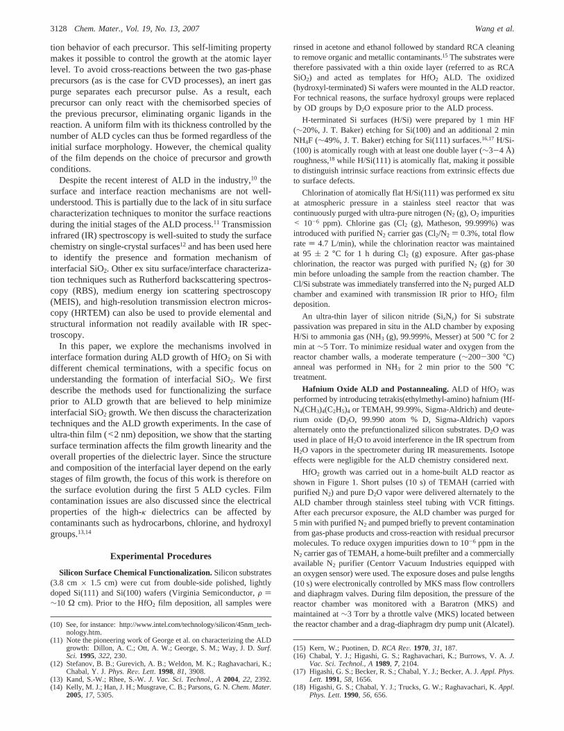
Figure 1. Schematic diagram of the ALD reactor (not to scale) with a transmission IR spectrometer for in situ surface characterization. The KBr windowsare protected by gate valves during ALD precursor exposures. During growth, the chamber was maintained at 60°C.
Ultra-Thin Hafnium Oxide Films Grown on Silicon by ALD Chem. Mater., Vol. 19, No. 13, 20073129
(O/Si), and silicon nitride (SixNy/Si). The ability to preventsilicon oxidation during HfO2 atomic layer growth is thenevaluated for these four surface terminations.
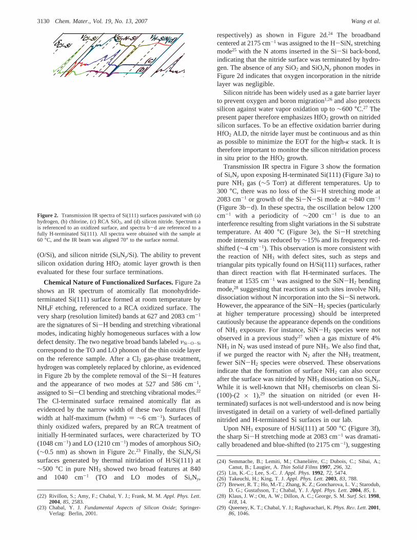
Chemical Nature of Functionalized Surfaces.Figure 2ashows an IR spectrum of atomically flat monohydride-terminated Si(111) surface formed at room temperature byNH4F etching, referenced to a RCA oxidized surface. Thevery sharp (resolution limited) bands at 627 and 2083 cm-1
are the signatures of Si-H bending and stretching vibrationalmodes, indicating highly homogeneous surfaces with a lowdefect density. The two negative broad bands labeledνSi-O-Si
correspond to the TO and LO phonon of the thin oxide layeron the reference sample. After a Cl2 gas-phase treatment,hydrogen was completely replaced by chlorine, as evidencedin Figure 2b by the complete removal of the Si-H featuresand the appearance of two modes at 527 and 586 cm-1,assigned to Si-Cl bending and stretching vibrational modes.22
The Cl-terminated surface remained atomically flat asevidenced by the narrow width of these two features (fullwidth at half-maximum (fwhm)) ∼6 cm-1). Surfaces ofthinly oxidized wafers, prepared by an RCA treatment ofinitially H-terminated surfaces, were characterized by TO(1048 cm-1) and LO (1210 cm-1) modes of amorphous SiO2(∼0.5 nm) as shown in Figure 2c.23 Finally, the SixNy/Sisurfaces generated by thermal nitridation of H/Si(111) at∼500 °C in pure NH3 showed two broad features at 840and 1040 cm-1 (TO and LO modes of SixNy,
respectively) as shown in Figure 2d.24 The broadbandcentered at 2175 cm-1 was assigned to the H-SiNx stretchingmode25 with the N atoms inserted in the Si-Si back-bond,indicating that the nitride surface was terminated by hydro-gen. The absence of any SiO2 and SiOxNy phonon modes inFigure 2d indicates that oxygen incorporation in the nitridelayer was negligible.
Silicon nitride has been widely used as a gate barrier layerto prevent oxygen and boron migration1,26 and also protectssilicon against water vapor oxidation up to∼600 °C.27 Thepresent paper therefore emphasizes HfO2 growth on nitridedsilicon surfaces. To be an effective oxidation barrier duringHfO2 ALD, the nitride layer must be continuous and as thinas possible to minimize the EOT for the high-κ stack. It istherefore important to monitor the silicon nitridation processin situ prior to the HfO2 growth.
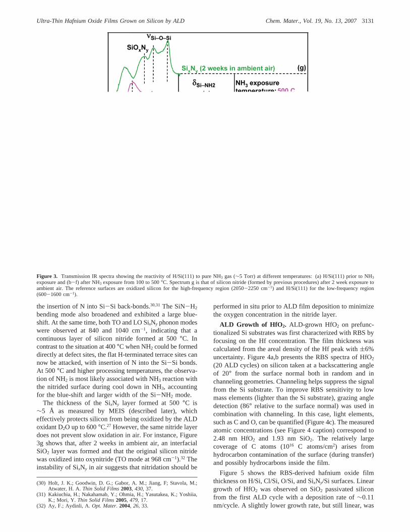
Transmission IR spectra in Figure 3 show the formationof SixNy upon exposing H-terminated Si(111) (Figure 3a) topure NH3 gas (∼5 Torr) at different temperatures. Up to300 °C, there was no loss of the Si-H stretching mode at2083 cm-1 or growth of the Si-N-Si mode at∼840 cm-1
(Figure 3b-d). In these spectra, the oscillation below 1200cm-1 with a periodicity of ∼200 cm-1 is due to aninterference resulting from slight variations in the Si substratetemperature. At 400°C (Figure 3e), the Si-H stretchingmode intensity was reduced by∼15% and its frequency red-shifted (∼4 cm-1). This observation is more consistent withthe reaction of NH3 with defect sites, such as steps andtriangular pits typically found on H/Si(111) surfaces, ratherthan direct reaction with flat H-terminated surfaces. Thefeature at 1535 cm-1 was assigned to the SiN-H2 bendingmode,28 suggesting that reactions at such sites involve NH3
dissociation without N incorporation into the Si-Si network.However, the appearance of the SiN-H2 species (particularlyat higher temperature processing) should be interpretedcautiously because the appearance depends on the conditionsof NH3 exposure. For instance, SiN-H2 species were notobserved in a previous study27 when a gas mixture of 4%NH3 in N2 was used instead of pure NH3. We also find that,if we purged the reactor with N2 after the NH3 treatment,fewer SiN-H2 species were observed. These observationsindicate that the formation of surface NH2 can also occurafter the surface was nitrided by NH3 dissociation on SixNy.While it is well-known that NH3 chemisorbs on clean Si-(100)-(2 × 1),29 the situation on nitrided (or even H-terminated) surfaces is not well-understood and is now beinginvestigated in detail on a variety of well-defined partiallynitrided and H-terminated Si surfaces in our lab.
Upon NH3 exposure of H/Si(111) at 500°C (Figure 3f),the sharp Si-H stretching mode at 2083 cm-1 was dramati-cally broadened and blue-shifted (to 2175 cm-1), suggesting
(22) Rivillon, S.; Amy, F.; Chabal, Y. J.; Frank, M. M.Appl. Phys. Lett.2004, 85, 2583.
(23) Chabal, Y. J.Fundamental Aspects of Silicon Oxide; Springer-Verlag: Berlin, 2001.
(24) Semmache, B.; Lemiti, M.; Chanelie´re, C.; Dubois, C.; Sibai, A.;Canut, B.; Laugier, A.Thin Solid Films1997, 296, 32.
(25) Lin, K.-C.; Lee, S.-C.J. Appl. Phys.1992, 72, 5474.(26) Takeuchi, H.; King, T. J.Appl. Phys. Lett.2003, 83, 788.(27) Brewer, R. T.; Ho, M.-T.; Zhang, K. Z.; Goncharova, L. V.; Starodub,
D. G.; Gustafsson, T.; Chabal, Y. J.Appl. Phys. Lett. 2004, 85, 1.(28) Klaus, J. W.; Ott, A. W.; Dillon, A. C.; George, S. M.Surf. Sci.1998,
418, 14.(29) Queeney, K. T.; Chabal, Y. J.; Raghavachari, K.Phys. ReV. Lett. 2001,
86, 1046.
Figure 2. Transmission IR spectra of Si(111) surfaces passivated with (a)hydrogen, (b) chlorine, (c) RCA SiO2, and (d) silicon nitride. Spectrum ais referenced to an oxidized surface, and spectra b-d are referenced to afully H-terminated Si(111). All spectra were obtained with the sample at60 °C, and the IR beam was aligned 70° to the surface normal.
3130 Chem. Mater., Vol. 19, No. 13, 2007 Wang et al.
the insertion of N into Si-Si back-bonds.30,31 The SiN-H2
bending mode also broadened and exhibited a large blue-shift. At the same time, both TO and LO SixNy phonon modeswere observed at 840 and 1040 cm-1, indicating that acontinuous layer of silicon nitride formed at 500°C. Incontrast to the situation at 400°C when NH2 could be formeddirectly at defect sites, the flat H-terminated terrace sites cannow be attacked, with insertion of N into the Si-Si bonds.At 500 °C and higher processing temperatures, the observa-tion of NH2 is most likely associated with NH3 reaction withthe nitrided surface during cool down in NH3, accountingfor the blue-shift and larger width of the Si-NH2 mode.
The thickness of the SixNy layer formed at 500°C is∼5 Å as measured by MEIS (described later), whicheffectively protects silicon from being oxidized by the ALDoxidant D2O up to 600°C.27 However, the same nitride layerdoes not prevent slow oxidation in air. For instance, Figure3g shows that, after 2 weeks in ambient air, an interfacialSiO2 layer was formed and that the original silicon nitridewas oxidized into oxynitride (TO mode at 968 cm-1).32 Theinstability of SixNy in air suggests that nitridation should be
performed in situ prior to ALD film deposition to minimizethe oxygen concentration in the nitride layer.
ALD Growth of HfO 2. ALD-grown HfO2 on prefunc-tionalized Si substrates was first characterized with RBS byfocusing on the Hf concentration. The film thickness wascalculated from the areal density of the Hf peak with(6%uncertainty. Figure 4a,b presents the RBS spectra of HfO2
(20 ALD cycles) on silicon taken at a backscattering angleof 20° from the surface normal both in random and inchanneling geometries. Channeling helps suppress the signalfrom the Si substrate. To improve RBS sensitivity to lowmass elements (lighter than the Si substrate), grazing angledetection (86° relative to the surface normal) was used incombination with channeling. In this case, light elements,such as C and O, can be quantified (Figure 4c). The measuredatomic concentrations (see Figure 4 caption) correspond to2.48 nm HfO2 and 1.93 nm SiO2. The relatively largecoverage of C atoms (1016 C atoms/cm2) arises fromhydrocarbon contamination of the surface (during transfer)and possibly hydrocarbons inside the film.
Figure 5 shows the RBS-derived hafnium oxide filmthickness on H/Si, Cl/Si, O/Si, and SixNy/Si surfaces. Lineargrowth of HfO2 was observed on SiO2 passivated siliconfrom the first ALD cycle with a deposition rate of∼0.11nm/cycle. A slightly lower growth rate, but still linear, was
(30) Holt, J. K.; Goodwin, D. G.; Gabor, A. M.; Jiang, F; Stavola, M.;Atwater, H. A.Thin Solid Films2003, 430, 37.
(31) Kakiuchia, H.; Nakahamab, Y.; Ohmia, H.; Yasutakea, K.; Yoshiia,K.; Mori, Y. Thin Solid Films2005, 479, 17.
(32) Ay, F.; Aydinli, A. Opt. Mater. 2004, 26, 33.
Figure 3. Transmission IR spectra showing the reactivity of H/Si(111) to pure NH3 gas (∼5 Torr) at different temperatures: (a) H/Si(111) prior to NH3
exposure and (b-f) after NH3 exposure from 100 to 500°C. Spectrum g is that of silicon nitride (formed by previous procedures) after 2 week exposure toambient air. The reference surfaces are oxidized silicon for the high-frequency region (2050-2250 cm-1) and H/Si(111) for the low-frequency region(600-1600 cm-1).
Ultra-Thin Hafnium Oxide Films Grown on Silicon by ALD Chem. Mater., Vol. 19, No. 13, 20073131
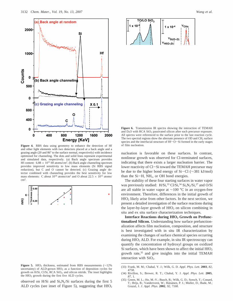
observed on H/Si and SixNy/Si surfaces during the first 5ALD cycles (see inset of Figure 5), suggesting that HfO2
nucleation is favorable on these surfaces. In contrast,nonlinear growth was observed for Cl-terminated surfaces,indicating that there exists a larger nucleation barrier. Thelower reactivity of Cl-Si toward the TEMAH precursor maybe due to the higher bond energy of Si-Cl (∼381 kJ/mol)than the Si-H, NHx, or OH bond energies.
The stability of these four starting surfaces in water vaporwas previously studied: H/Si,33 Cl/Si,34 SixNy/Si,27 and O/Siare all stable in water vapor at∼100 °C in an oxygen-freeenvironment. Therefore, differences in the initial growth ofHfO2 likely arise from other factors. In the next section, wepresent a detailed investigation of the surface reactions duringthe layer-by-layer growth of HfO2 on silicon combining insitu and ex situ surface characterization techniques.
Interface Reactions during HfO2 Growth on Prefunc-tionalized Silicon. Understanding how surface prefunction-alization affects film nucleation, composition, and structureis best investigated with in situ IR characterization byexamining the changes of surface chemical species occurringduring HfO2 ALD. For example, in situ IR spectroscopy canquantify the concentration of hydroxyl groups on oxidizedSi surfaces, which have been shown to affect the initial HfO2
growth rate,35 and give insights into the initial TEMAHinteraction with SiO2.
(33) Frank, M. M.; Chabal, Y. J.; Wilk, G. D.Appl. Phys. Lett. 2003, 82,4758.
(34) Rivillon, S.; Brewer, R. T.; Chabal, Y. J.Appl. Phys. Lett. 2005,87, 1.
(35) Green, M. L.; Ho, M.-Y.; Busch, B.; Wilk, G. D.; Sorsch, T.; Conard,T.; Brijs, B.; Vandervorst, W.; Ra`isanen, P. I.; Muller, D.; Bude, M.;Grazul, J.J. Appl. Phys.2002, 92, 7168.
Figure 4. RBS data using geometry to enhance the detection of Hfand other light elements with two detectors placed at a back angle and agrazing angle (20 and 86° to the surface normal, respectively) with incidenceoptimized for channeling. The dots and solid lines represent experimentaland simulated data, respectively. (a) Back angle spectrum providesHf content: 6.88× 10¹⁵ Hf atoms/cm2. (b) Back angle channeling spectrumprovides improved sensitivity to low mass elements (Si RBS signalreduction), but C and O cannot be detected. (c) Grazing angle de-tector combined with channeling provides the best sensitivity for lowmass elements: C about 1016 atoms/cm2 and O about 22.5× 10¹⁵ atoms/cm2.
Figure 5. HfO2 thickness, estimated from RBS measurements (∼12%uncertainty) of ALD-grown HfO2 as a function of deposition cycles forgrowth on H/Si, Cl/Si, RCA SiO2, and silicon nitride. The inset highlightsthe HfO2 growth during the first five ALD cycles.
Figure 6. Transmission IR spectra showing the interaction of TEMAHand D2O with RCA SiO2 passivated silicon after each precursor exposure.All spectra were referenced to the surface prior to the last reaction cycle.The two spectral regions show the alternate presence of OD and CHx surfacespecies and the interfacial structure of Hf-O-Si formed in the early stagesof film nucleation.
3132 Chem. Mater., Vol. 19, No. 13, 2007 Wang et al.
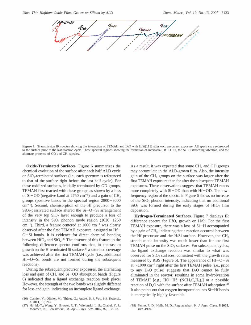
Oxide-Terminated Surfaces.Figure 6 summarizes thechemical evolution of the surface after each half ALD cycleon SiO2-terminated surfaces (i.e., each spectrum is referencedto that of the surface right before the last half cycle). Forthese oxidized surfaces, initially terminated by OD groups,TEMAH first reacted with these groups as shown by a lossof Si-OD (negative band at 2750 cm-1) and a gain of CHxgroups (positive bands in the spectral region 2800-3000cm-1). Second, chemisorption of the Hf precursor to theSiO2-passivated surface altered the Si-O-Si arrangementof the very top SiO2 layer enough to produce a loss ofintensity in the SiO2 phonon mode region (1020-1250cm-1). Third, a feature centered at 1000 cm-1 was clearlyobserved after the first TEMAH exposure, assigned to Hf-O-Si bonds. It is evidence for direct chemical bondingbetween HfO2 and SiO2.36 The absence of this feature in thefollowing difference spectra confirms that, in contrast togrowth on the H-terminated Si surface,37 a saturated coveragewas achieved after the first TEMAH cycle (i.e., additionalHf-O-Si bonds are not formed during the subsequentreactions).
During the subsequent precursor exposures, the alternatingloss and gain of CHx and Si-OD absorption bands (Figure6) indicated that a ligand exchange reaction took place.However, the strength of the two bands was slightly differentfor loss and gain, indicating an incomplete ligand exchange.
As a result, it was expected that some CHx and OD groupsmay accumulate in the ALD-grown film. Also, the intensitygain of the CHx groups on the surface was larger after thefirst TEMAH exposure than for after the subsequent TEMAHexposures. These observations suggest that TEMAH reactsmore completely with Si-OD than with Hf-OD. The low-frequency region of the spectra in Figure 6 shows no increaseof the SiO2 phonon intensity, indicating that no additionalSiO2 was formed during the early stages of HfO2 filmdeposition.
Hydrogen-Terminated Surfaces.Figure 7 displays IRdifference spectra for HfO2 growth on H/Si. For the firstTEMAH exposure, there was a loss of Si-H accompaniedby a gain of CHx, indicating that a reaction occurred betweenthe Hf precursor and the H/Si surface. However, the CHx
stretch mode intensity was much lower than for the firstTEMAH pulse on the SiO2 surfaces. For subsequent cycles,the ligand exchange reaction was similar to what wasobserved for SiO2 surfaces, consistent with the growth ratesmeasured by RBS (Figure 5). The appearance of Hf-O-Siat∼1000 cm-1 right after the first TEMAH pulse (i.e., priorto any D2O pulse) suggests that D2O cannot be fullyeliminated in the reactor, resulting in some hydrolyzationof TEMAH [e.g., HO-Hf-(NCH3C2H5)3] or a possiblereaction of D2O with the surface after TEMAH adsorption.38
It also points out that oxygen incorporation into Si-Hf bondsis energetically highly favorable.
(36) Cosnier, V.; Olivier, M.; The´ret, G.; Andre, B. J. Vac. Sci. Technol.,A 2001, 19, 267.
(37) Ho, M.-T.; Wang, Y.; Brewer, R. T.; Wielunski, L. S.; Chabal, Y. J.;Moumen, N.; Boleslawski, M.Appl. Phys. Lett. 2005, 87, 133103.
(38) Fenno, R. D.; Halls, M. D.; Raghavachari, K.J. Phys. Chem. B2005,109, 4969.
Figure 7. Transmission IR spectra showing the interaction of TEMAH and D2O with H/Si(111) after each precursor exposure. All spectra are referencedto the surface prior to the last reaction cycle. Three spectral regions showing the formation of interfacial Hf-O-Si, the Si-H stretching vibration, and thealternate presence of OD and CHx species.
Ultra-Thin Hafnium Oxide Films Grown on Silicon by ALD Chem. Mater., Vol. 19, No. 13, 20073133
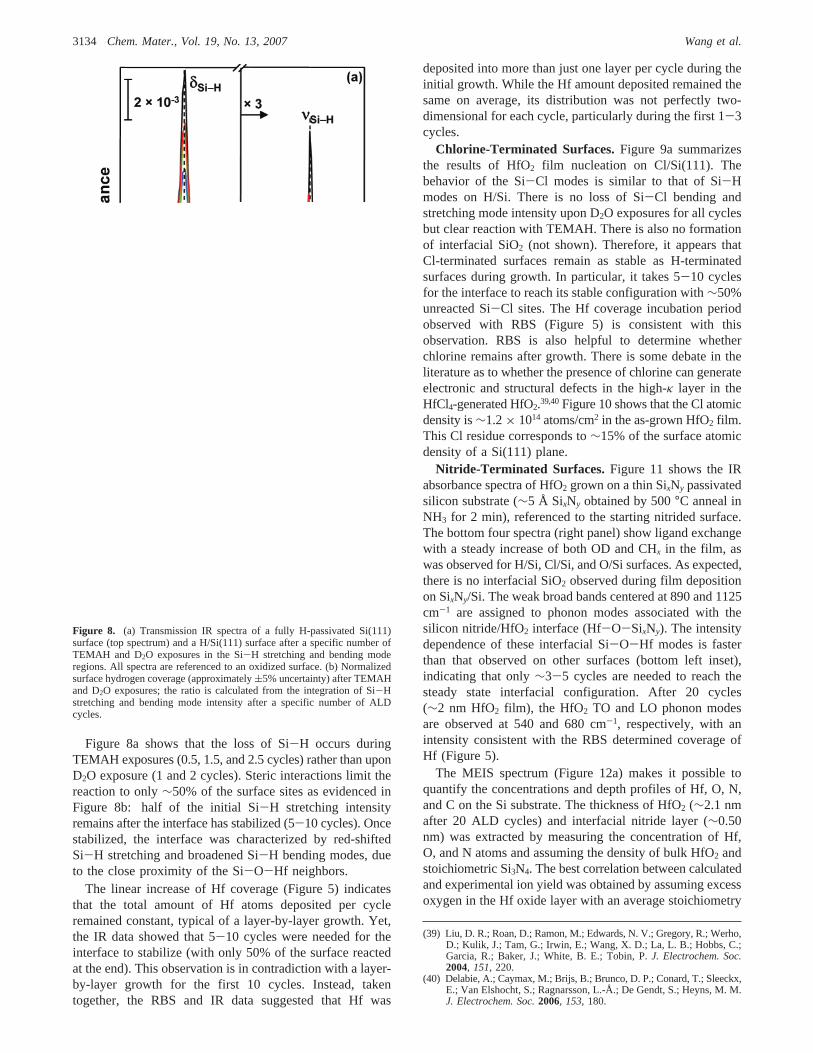
Figure 8a shows that the loss of Si-H occurs duringTEMAH exposures (0.5, 1.5, and 2.5 cycles) rather than uponD2O exposure (1 and 2 cycles). Steric interactions limit thereaction to only∼50% of the surface sites as evidenced inFigure 8b: half of the initial Si-H stretching intensityremains after the interface has stabilized (5-10 cycles). Oncestabilized, the interface was characterized by red-shiftedSi-H stretching and broadened Si-H bending modes, dueto the close proximity of the Si-O-Hf neighbors.
The linear increase of Hf coverage (Figure 5) indicatesthat the total amount of Hf atoms deposited per cycleremained constant, typical of a layer-by-layer growth. Yet,the IR data showed that 5-10 cycles were needed for theinterface to stabilize (with only 50% of the surface reactedat the end). This observation is in contradiction with a layer-by-layer growth for the first 10 cycles. Instead, takentogether, the RBS and IR data suggested that Hf was
deposited into more than just one layer per cycle during theinitial growth. While the Hf amount deposited remained thesame on average, its distribution was not perfectly two-dimensional for each cycle, particularly during the first 1-3cycles.
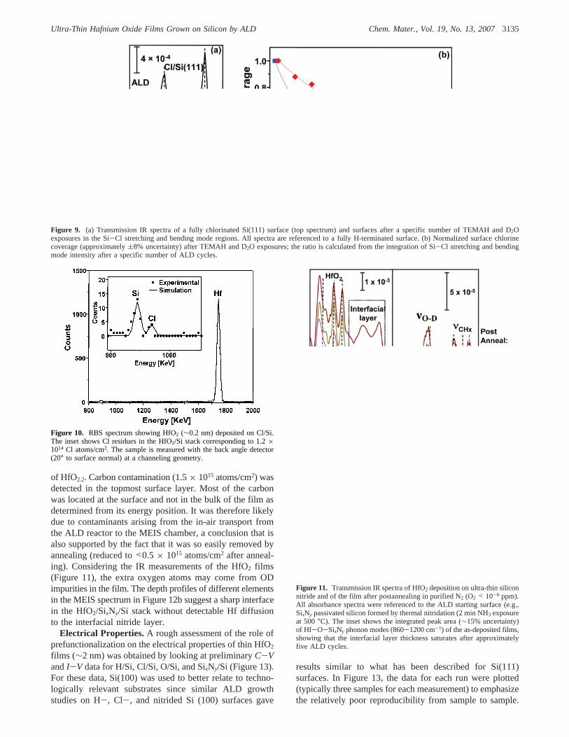
Chlorine-Terminated Surfaces. Figure 9a summarizesthe results of HfO2 film nucleation on Cl/Si(111). Thebehavior of the Si-Cl modes is similar to that of Si-Hmodes on H/Si. There is no loss of Si-Cl bending andstretching mode intensity upon D2O exposures for all cyclesbut clear reaction with TEMAH. There is also no formationof interfacial SiO2 (not shown). Therefore, it appears thatCl-terminated surfaces remain as stable as H-terminatedsurfaces during growth. In particular, it takes 5-10 cyclesfor the interface to reach its stable configuration with∼50%unreacted Si-Cl sites. The Hf coverage incubation periodobserved with RBS (Figure 5) is consistent with thisobservation. RBS is also helpful to determine whetherchlorine remains after growth. There is some debate in theliterature as to whether the presence of chlorine can generateelectronic and structural defects in the high-κ layer in theHfCl4-generated HfO2.39,40Figure 10 shows that the Cl atomicdensity is∼1.2× 10¹⁴ atoms/cm2 in the as-grown HfO2 film.This Cl residue corresponds to∼15% of the surface atomicdensity of a Si(111) plane.
Nitride-Terminated Surfaces. Figure 11 shows the IRabsorbance spectra of HfO2 grown on a thin SixNy passivatedsilicon substrate (∼5 Å SixNy obtained by 500°C anneal inNH3 for 2 min), referenced to the starting nitrided surface.The bottom four spectra (right panel) show ligand exchangewith a steady increase of both OD and CHx in the film, aswas observed for H/Si, Cl/Si, and O/Si surfaces. As expected,there is no interfacial SiO2 observed during film depositionon SixNy/Si. The weak broad bands centered at 890 and 1125cm-1 are assigned to phonon modes associated with thesilicon nitride/HfO2 interface (Hf-O-SixNy). The intensitydependence of these interfacial Si-O-Hf modes is fasterthan that observed on other surfaces (bottom left inset),indicating that only∼3-5 cycles are needed to reach thesteady state interfacial configuration. After 20 cycles(∼2 nm HfO2 film), the HfO2 TO and LO phonon modesare observed at 540 and 680 cm-1, respectively, with anintensity consistent with the RBS determined coverage ofHf (Figure 5).
The MEIS spectrum (Figure 12a) makes it possible toquantify the concentrations and depth profiles of Hf, O, N,and C on the Si substrate. The thickness of HfO2 (∼2.1 nmafter 20 ALD cycles) and interfacial nitride layer (∼0.50nm) was extracted by measuring the concentration of Hf,O, and N atoms and assuming the density of bulk HfO2 andstoichiometric Si3N4. The best correlation between calculatedand experimental ion yield was obtained by assuming excessoxygen in the Hf oxide layer with an average stoichiometry
(39) Liu, D. R.; Roan, D.; Ramon, M.; Edwards, N. V.; Gregory, R.; Werho,D.; Kulik, J.; Tam, G.; Irwin, E.; Wang, X. D.; La, L. B.; Hobbs, C.;Garcia, R.; Baker, J.; White, B. E.; Tobin, P.J. Electrochem. Soc.2004, 151, 220.
(40) Delabie, A.; Caymax, M.; Brijs, B.; Brunco, D. P.; Conard, T.; Sleeckx,E.; Van Elshocht, S.; Ragnarsson, L.-Å.; De Gendt, S.; Heyns, M. M.J. Electrochem. Soc.2006, 153, 180.
Figure 8. (a) Transmission IR spectra of a fully H-passivated Si(111)surface (top spectrum) and a H/Si(111) surface after a specific number ofTEMAH and D2O exposures in the Si-H stretching and bending moderegions. All spectra are referenced to an oxidized surface. (b) Normalizedsurface hydrogen coverage (approximately(5% uncertainty) after TEMAHand D2O exposures; the ratio is calculated from the integration of Si-Hstretching and bending mode intensity after a specific number of ALDcycles.
3134 Chem. Mater., Vol. 19, No. 13, 2007 Wang et al.
of HfO2.2. Carbon contamination (1.5× 10¹⁵ atoms/cm2) wasdetected in the topmost surface layer. Most of the carbonwas located at the surface and not in the bulk of the film asdetermined from its energy position. It was therefore likelydue to contaminants arising from the in-air transport fromthe ALD reactor to the MEIS chamber, a conclusion that isalso supported by the fact that it was so easily removed byannealing (reduced to<0.5 × 10¹⁵ atoms/cm2 after anneal-ing). Considering the IR measurements of the HfO2 films(Figure 11), the extra oxygen atoms may come from ODimpurities in the film. The depth profiles of different elementsin the MEIS spectrum in Figure 12b suggest a sharp interfacein the HfO2/SixNy/Si stack without detectable Hf diffusionto the interfacial nitride layer.
Electrical Properties. A rough assessment of the role ofprefunctionalization on the electrical properties of thin HfO2
films (∼2 nm) was obtained by looking at preliminaryC-VandI-V data for H/Si, Cl/Si, O/Si, and SixNy/Si (Figure 13).For these data, Si(100) was used to better relate to techno-logically relevant substrates since similar ALD growthstudies on H-, Cl-, and nitrided Si (100) surfaces gave
results similar to what has been described for Si(111)surfaces. In Figure 13, the data for each run were plotted(typically three samples for each measurement) to emphasizethe relatively poor reproducibility from sample to sample.
Figure 9. (a) Transmission IR spectra of a fully chlorinated Si(111) surface (top spectrum) and surfaces after a specific number of TEMAH and D2Oexposures in the Si-Cl stretching and bending mode regions. All spectra are referenced to a fully H-terminated surface. (b) Normalized surface chlorinecoverage (approximately(8% uncertainty) after TEMAH and D2O exposures; the ratio is calculated from the integration of Si-Cl stretching and bendingmode intensity after a specific number of ALD cycles.
Figure 10. RBS spectrum showing HfO2 (∼0.2 nm) deposited on Cl/Si.The inset shows Cl residues in the HfO2/Si stack corresponding to 1.2×10¹⁴ Cl atoms/cm2. The sample is measured with the back angle detector(20° to surface normal) at a channeling geometry.
Figure 11. Transmission IR spectra of HfO2 deposition on ultra-thin siliconnitride and of the film after postannealing in purified N2 (O2 < 10-6 ppm).All absorbance spectra were referenced to the ALD starting surface (e.g.,SixNy passivated silicon formed by thermal nitridation (2 min NH3 exposureat 500°C). The inset shows the integrated peak area (∼15% uncertainty)of Hf-O-SixNy phonon modes (860-1200 cm-1) of the as-deposited films,showing that the interfacial layer thickness saturates after approximatelyfive ALD cycles.
Ultra-Thin Hafnium Oxide Films Grown on Silicon by ALD Chem. Mater., Vol. 19, No. 13, 20073135
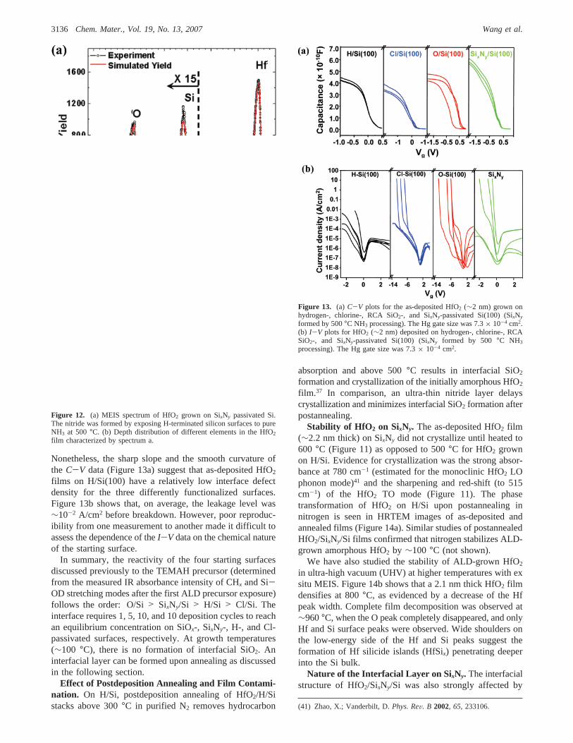
Nonetheless, the sharp slope and the smooth curvature ofthe C-V data (Figure 13a) suggest that as-deposited HfO2
films on H/Si(100) have a relatively low interface defectdensity for the three differently functionalized surfaces.Figure 13b shows that, on average, the leakage level was∼10-2 A/cm2 before breakdown. However, poor reproduc-ibility from one measurement to another made it difficult toassess the dependence of theI-V data on the chemical natureof the starting surface.
In summary, the reactivity of the four starting surfacesdiscussed previously to the TEMAH precursor (determinedfrom the measured IR absorbance intensity of CHx and Si-OD stretching modes after the first ALD precursor exposure)follows the order: O/Si> SixNy/Si > H/Si > Cl/Si. Theinterface requires 1, 5, 10, and 10 deposition cycles to reachan equilibrium concentration on SiOx-, SixNy-, H-, and Cl-passivated surfaces, respectively. At growth temperatures(∼100 °C), there is no formation of interfacial SiO2. Aninterfacial layer can be formed upon annealing as discussedin the following section.
Effect of Postdeposition Annealing and Film Contami-nation. On H/Si, postdeposition annealing of HfO2/H/Sistacks above 300°C in purified N2 removes hydrocarbon
absorption and above 500°C results in interfacial SiO2formation and crystallization of the initially amorphous HfO2
film.37 In comparison, an ultra-thin nitride layer delayscrystallization and minimizes interfacial SiO2 formation afterpostannealing.
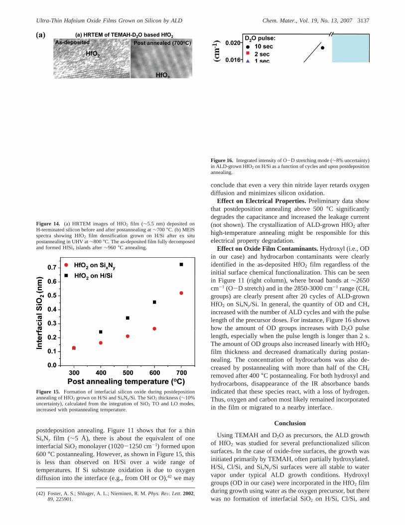
Stability of HfO 2 on SixNy. The as-deposited HfO2 film(∼2.2 nm thick) on SixNy did not crystallize until heated to600 °C (Figure 11) as opposed to 500°C for HfO2 grownon H/Si. Evidence for crystallization was the strong absor-bance at 780 cm-1 (estimated for the monoclinic HfO2 LOphonon mode)41 and the sharpening and red-shift (to 515cm-1) of the HfO2 TO mode (Figure 11). The phasetransformation of HfO2 on H/Si upon postannealing innitrogen is seen in HRTEM images of as-deposited andannealed films (Figure 14a). Similar studies of postannealedHfO2/SixNy/Si films confirmed that nitrogen stabilizes ALD-grown amorphous HfO2 by ∼100 °C (not shown).
We have also studied the stability of ALD-grown HfO2
in ultra-high vacuum (UHV) at higher temperatures with exsitu MEIS. Figure 14b shows that a 2.1 nm thick HfO2 filmdensifies at 800°C, as evidenced by a decrease of the Hfpeak width. Complete film decomposition was observed at∼960°C, when the O peak completely disappeared, and onlyHf and Si surface peaks were observed. Wide shoulders onthe low-energy side of the Hf and Si peaks suggest theformation of Hf silicide islands (HfSix) penetrating deeperinto the Si bulk.
Nature of the Interfacial Layer on SixNy. The interfacialstructure of HfO2/SixNy/Si was also strongly affected by
(41) Zhao, X.; Vanderbilt, D.Phys. ReV. B 2002, 65, 233106.
Figure 12. (a) MEIS spectrum of HfO2 grown on SixNy passivated Si.The nitride was formed by exposing H-terminated silicon surfaces to pureNH3 at 500°C. (b) Depth distribution of different elements in the HfO2
film characterized by spectrum a.
Figure 13. (a) C-V plots for the as-deposited HfO2 (∼2 nm) grown onhydrogen-, chlorine-, RCA SiO2-, and SixNy-passivated Si(100) (SixNy
formed by 500°C NH3 processing). The Hg gate size was 7.3× 10⁻⁴ cm2.(b) I-V plots for HfO2 (∼2 nm) deposited on hydrogen-, chlorine-, RCASiO2-, and SixNy-passivated Si(100) (SixNy formed by 500 °C NH3
processing). The Hg gate size was 7.3× 10⁻⁴ cm2.
3136 Chem. Mater., Vol. 19, No. 13, 2007 Wang et al.
postdeposition annealing. Figure 11 shows that for a thinSixNy film (∼5 Å), there is about the equivalent of oneinterfacial SiO2 monolayer (1020-1250 cm-1) formed upon600°C postannealing. However, as shown in Figure 15, thisis less than observed on H/Si over a wide range oftemperatures. If Si substrate oxidation is due to oxygendiffusion into the interface (e.g., from OH or O),42 we may
conclude that even a very thin nitride layer retards oxygendiffusion and minimizes silicon oxidation.
Effect on Electrical Properties. Preliminary data showthat postdeposition annealing above 500°C significantlydegrades the capacitance and increased the leakage current(not shown). The crystallization of ALD-grown HfO2 afterhigh-temperature annealing might be responsible for thiselectrical property degradation.
Effect on Oxide Film Contaminants.Hydroxyl (i.e., ODin our case) and hydrocarbon contaminants were clearlyidentified in the as-deposited HfO2 film regardless of theinitial surface chemical functionalization. This can be seenin Figure 11 (right column), where broad bands at∼2650cm-1 (O-D stretch) and in the 2850-3000 cm-1 range (CHx
groups) are clearly present after 20 cycles of ALD-grownHfO2 on SixNy/Si. In general, the quantity of OD and CHx
increased with the number of ALD cycles and with the pulselength of the precursor doses. For instance, Figure 16 showshow the amount of OD groups increases with D2O pulselength, especially when the pulse length is longer than 2 s.The amount of OD groups also increased linearly with HfO2
film thickness and decreased dramatically during postan-nealing. The concentration of hydrocarbons was also de-creased by postannealing with more than half of the CHx
removed after 400°C postannealing. For both hydroxyl andhydrocarbons, disappearance of the IR absorbance bandsindicated that these species react, with a loss of hydrogen.Thus, oxygen and carbon most likely remained incorporatedin the film or migrated to a nearby interface.
Conclusion
Using TEMAH and D2O as precursors, the ALD growthof HfO2 was studied for several prefunctionalized siliconsurfaces. In the case of oxide-free surfaces, the growth wasinitiated primarily by TEMAH, often partially hydroxylated.H/Si, Cl/Si, and SixNy/Si surfaces were all stable to watervapor under typical ALD growth conditions. Hydroxylgroups (OD in our case) were incorporated in the HfO2 filmduring growth using water as the oxygen precursor, but therewas no formation of interfacial SiO2 on H/Si, Cl/Si, and
(42) Foster, A. S.; Shluger, A. L.; Nieminen, R. M.Phys. ReV. Lett. 2002,89, 225901.
Figure 14. (a) HRTEM images of HfO2 film (∼5.5 nm) deposited onH-terminated silicon before and after postannealing at∼700°C. (b) MEISspectra showing HfO2 film densification grown on H/Si after ex situpostannealing in UHV at∼800°C. The as-deposited film fully decomposedand formed HfSix islands after∼960 °C annealing.
Figure 15. Formation of interfacial silicon oxide during postdepositionannealing of HfO2 grown on H/Si and SixNy/Si. The SiO2 thickness (∼10%uncertainty), calculated from the integration of SiO2 TO and LO modes,increased with postannealing temperature.
Figure 16. Integrated intensity of O-D stretching mode (∼8% uncertainty)in ALD-grown HfO2 on H/Si as a function of cycles and upon postdepositionannealing.
Ultra-Thin Hafnium Oxide Films Grown on Silicon by ALD Chem. Mater., Vol. 19, No. 13, 20073137
SixNy/Si at the growth conditions. These hydroxyl speciesled to excess oxygen (forming HfO2.2 films).
Linear growth on the hydroxylated SiO2 surface wasobserved in both RBS and IR spectra from the very beginningof the film nucleation with a deposition rate of∼0.11 nmper ALD cycle. For H/Si and SixNy surfaces, several cycleswere required for the interface to reach its equilibriumcomposition, although the Hf coverage increased linearly.This apparent contradiction suggests that Hf was not neces-sarily deposited within a two-dimensional layer (in a perfectlayer-per-layer growth mode) during the early cycles butinvolved instead a rougher growth mode on the microscopicscale initially. For Cl/Si surfaces, both RBS and IR showedan incubation period. The relative reactivity to TEMAH forthese surface functionalizations was O/Si> SixNy/Si > H/Si> Cl/Si.
The effect of postannealing on HfO2 film composition andHfO2/Si interfacial structure clearly showed that SiO2 began
to develop at the interface as the annealing temperature wasraised to 500°C for H-passivation and 600°C for nitridepassivation. On the other hand, postdeposition annealingeffectively removed (i.e., reacted with) ligand impurities (ODand CHx) from the HfO2 film. The formation of SiO2 afterpostdeposition annealing was consistent with OD radicalsdiffusing to the HfO2/Si interface and oxidizing the substratesilicon, although potential diffusion of O2 and D2O from theambient cannot be completely ruled out. An ultra-thin nitridelayer effectively prevented oxygen diffusion and minimizedinterfacial SiO2 formation.
Acknowledgment. This work was supported by the NationalScience Foundation (Grant CHE-0415652) and SEMATECH.L.V.G. and T.G. acknowledge support from the NSF (GrantDMR-0218406). The authors thank Eric L. Garfunkel, RhettT. Brewer, and Kenneth Bratland for insightful discussions.
CM061761P
3138 Chem. Mater., Vol. 19, No. 13, 2007 Wang et al.


![Hafnium-based High-k Gate Dielectricscdn.intechweb.org/pdfs/9848.pdf · Hafnium-based High-k Gate Dielectrics 335 Fig. 3. Schematic of direct tunneling through SiO2 [3]. Gate electrode](https://img.pdfslide.us/doc/110x75/5af9caca7f8b9a44658e3135/hafnium-based-high-k-gate-high-k-gate-dielectrics-335-fig-3-schematic-of-direct.jpg)