Embed Size (px)
Citation preview
www.elsevier.com/locate/ultras
Ultrasonics 44 (2006) e1269–e1275
Characterization of Ta and TaN diffusion barriers beneathCu layers using picosecond ultrasonics
Juerg Bryner a,*, Dieter M. Profunser a,1, Jacqueline Vollmann a,Elisabeth Mueller b, Juerg Dual a
a Center of Mechanics, ETH Zurich, 8092 Zurich, Switzerlandb Laboratory for Solid State Physics, ETH Zurich, 8093 Zurich, Switzerland
Available online 6 June 2006
Abstract
In computer chips, aluminum is being replaced with copper in order to produce smaller, faster and more efficient electronic devices.The usage of copper allows higher current densities and thus higher packaging densities than aluminum. However, copper leads to newchallenges and problems. It has different mechanical properties and a tendency to migrate into the surrounding dielectric and/or semi-conducting layers. These diffusion processes can be prevented by so called diffusion barriers. A diffusion barrier is a very thin layer con-sisting of tantalum and tantalum nitride or titanium and titanium nitride, deposited between the copper and the substrate.
A pump-probe setup is used to determine the mechanical properties of the barrier layers and of the copper layer. This short-pulse-laser-acoustic method is contact-free and non-destructive. Mechanical waves are excited and detected thermoelastically using laser pulsesof 70 fs duration. Thin film measurements of buried diffusion layers are provided and compared with scanning electron microscopy(SEM), transmission electron microscopy (TEM), and Rutherford Backscattering Spectroscopy measurements (RBS). Results of athermo-elasto-mechanical simulation are presented and a short overview of the simulation procedure is given.
Current limits of the presented method are discussed and future directions of the on-going research project are presented.� 2006 Elsevier B.V. All rights reserved.
Keywords: Laser acoustic thin film metrology; Diffusion barrier measurement; Photoacoustic detection; In-depth profiling; Photoacoustic simulation
1. Introduction
Higher device speed and less electromigration areamong the main reasons for the semiconductor industry’stransition from Al-based metallization to a Cu-based met-allization. Cu-based metallization for ultra-large scale inte-grated (ULSI) devices led to numerous studies concerningits thermal stability as well as the deposition and etchingprocesses at the beginning of the past decade. However,among the drawbacks of the usage of Cu is its tendency
0041-624X/$ - see front matter � 2006 Elsevier B.V. All rights reserved.
doi:10.1016/j.ultras.2006.05.097
* Corresponding author. Tel.: +41 44 632 5293; fax: +41 44 632 1145.E-mail addresses: [email protected] (J. Bryner), dieter@
profunser.com (D.M. Profunser).1 Present address: Hokkaido University, Faculty of Engineering, Sap-
poro 060-8628, Japan. Tel.: +81 11 706 7817; fax: +81 11 706 7817.
to diffuse significantly into the surrounding dielectric mate-rials or semiconductors. Therefore a lining of the Cu-channels consisting of a Ta layer or a Ta/TaN bi-layer isrequired. The thickness of these diffusion barrier layersamounts to about 10 nm or less. The non-destructive mon-itoring of the deposition of such diffusion barrier layersduring the production process is challenging andimportant.
Cu-metallization, and in particular the transition to300 mm size wafers increases the need to monitor the cor-rect deposition of each layer and the measurement of itsthickness. Scanning electron microscopy (SEM), transmis-sion electron microscopy (TEM) and Rutherford backscat-tering spectroscopy measurements (RBS) represent highlypotent methods to analyze existing thin film multi-layers.While TEM provides an almost atomic resolution, RBS
e1270 J. Bryner et al. / Ultrasonics 44 (2006) e1269–e1275
provides a quantitative analysis of the chemical compoundof each single layer, its density, and its thickness. SEM andTEM require an extended preparation of the specimen inorder to obtain a plain and polished cross-section of themulti-layer or the structure of interest and are thereforedestructive methods. RBS demands extensive equipmentlike acceleration and ‘beam-forming’ devices of the He-ionsand devices for measuring the kinetic energy of the back-scattered ions. It does not require a special preparationof the specimen but provides only a limited lateral resolu-tion. Although the methods mentioned above permit amagnificent insight into structures at a resolution of fewnanometers, they are not suitable for the application inproduction environment.
Short-pulse-laser-ultrasonics, as introduced by Thomsenet al. [1,2], uses very short laser pulses having durations ofless than 100 fs in order to excite acoustic pulses i.e. bulkwaves thermoelastically. The ‘round-trip-time’ of theseacoustic pulses is measured with a pump-probe schemewhich is described in detail by Vollmann et al. [3]. Theadvantages of this method are its rapid, non-destructiveand non-contact manner although its in-depth-resolutioncannot compete with TEM or SEM.
2. Short-pulse-laser-ultrasonics (picosecond ultrasonics)
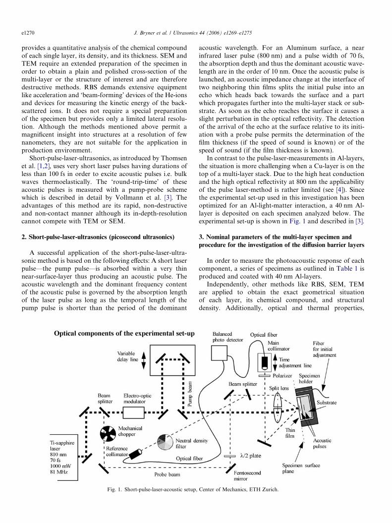
A successful application of the short-pulse-laser-ultra-sonic method is based on the following effects: A short laserpulse—the pump pulse—is absorbed within a very thinnear-surface-layer thus producing an acoustic pulse. Theacoustic wavelength and the dominant frequency contentof the acoustic pulse is governed by the absorption lengthof the laser pulse as long as the temporal length of thepump pulse is shorter than the period of the dominant
Fig. 1. Short-pulse-laser-acoustic setup,
acoustic wavelength. For an Aluminum surface, a nearinfrared laser pulse (800 nm) and a pulse width of 70 fs,the absorption depth and thus the dominant acoustic wave-length are in the order of 10 nm. Once the acoustic pulse islaunched, an acoustic impedance change at the interface oftwo neighboring thin films splits the initial pulse into anecho which heads back towards the surface and a partwhich propagates further into the multi-layer stack or sub-strate. As soon as the echo reaches the surface it causes aslight perturbation in the optical reflectivity. The detectionof the arrival of the echo at the surface relative to its initi-ation with a probe pulse permits the determination of thefilm thickness (if the speed of sound is known) or of thespeed of sound (if the film thickness is known).
In contrast to the pulse-laser-measurements in Al-layers,the situation is more challenging when a Cu-layer is on thetop of a multi-layer stack. Due to the high heat conductionand the high optical reflectivity at 800 nm the applicabilityof the pulse laser-method is rather limited (see [4]). Sincethe experimental set-up used in this investigation has beenoptimized for an Al-light-matter interaction, a 40 nm Al-layer is deposited on each specimen analyzed below. Theexperimental set-up is shown in Fig. 1 and described in [3].
3. Nominal parameters of the multi-layer specimen and
procedure for the investigation of the diffusion barrier layers
In order to measure the photoacoustic response of eachcomponent, a series of specimens as outlined in Table 1 isproduced and coated with 40 nm Al-layers.
Independently, other methods like RBS, SEM, TEMare applied to obtain the exact geometrical situationof each layer, its chemical compound, and structuraldensity. Additionally, optical and thermal properties,
Center of Mechanics, ETH Zurich.
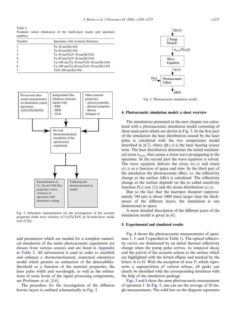
Table 1Nominal values (thickness) of the multi-layer stacks and specimennumbers
Number Specimen with nominal thickness
1 Ta 30 nm/Si(100)2 Ta 60 nm/Si(100)3 Ta 30 nm/TaN 30 nm/Si(100)4 Ta 60 nm/TaN 30 nm/Si(100)5 Cu 100 nm/Ta 30 nm/TaN 30 nm/Si(100)6 Cu 100 nm/Ta 60 nm/TaN 30 nm/Si(100)7 TaN 100 nm/Si(100)
Fig. 2. Schematic representation for the investigation of the acousticproperties (bulk wave velocity) of Cu/Ta/TaN on Si-multi-layer stacks(out of [6]).
Fig. 3. Photoacoustic simulation model.
J. Bryner et al. / Ultrasonics 44 (2006) e1269–e1275 e1271
and parameters which are needed for a complete numeri-cal simulation of the entire photoacoustic experiment arechosen from various sources and are listed in Appendixin Table 2. All information is used in order to establishand enhance a thermomechanical, numerical simulationmodel which permits an estimation of the detectability-threshold as a function of the material properties, thelaser pulse width and wavelength, as well as the estima-tions of noise levels of the signal processing components,see Profunser et al. [5,6].
The procedure for the investigation of the diffusionbarrier layers is outlined schematically in Fig. 2.
4. Photoacoustic simulation model: a short overview
The simulations presented in the next chapter are calcu-lated with a photoacoustic simulation model consisting ofthree main parts which are shown in Fig. 3. In the first partof the simulation the heat distribution caused by the laserpulse is calculated with the two temperature modeldescribed in [6,7], where Q(z, t) is the laser heating sourceterm. The heat distribution determines the initial mechani-cal stress rexcit, that causes a stress wave propagating in thespecimen. In the second part the wave equation is solved.The wave equation delivers the stress r(z, t) and straine(z, t) as a function of space and time. In the third part ofthe simulation the photoacoustic effect, i.e. the reflectivitychange at the surface DR(t) is calculated. The reflectivitychange at the surface depends on the so called sensitivityfunction F(z) (see [1]) and the strain distribution e(z, t).
Due to the fact that the laserspot diameter (approxi-mately 100 lm) is about 1000 times larger than the thick-nesses of the different layers, the simulation is onedimensional in space.
A more detailed description of the different parts of thesimulation model is given in [6].
5. Experimental and simulated results
Fig. 4 shows the photoacoustic measurements of speci-men 1, 3, and 5 (specified in Table 1). The optical reflectiv-ity curves are dominated by an initial thermal reflectivitychange when the pump pulse arrives, its temporal decayand the arrival of the acoustic echoes at the surface whichare highlighted with the dotted ellipsis and marked by theletters A to G. With the exception of area F, which repre-sents a superposition of various echoes, all peaks canclearly be identified with the corresponding interfaces withthe help of the simulation package.
Figs. 5 and 6 show the same photoacoustic measurementof specimen 1. In Fig. 5, one can see the average of 10 sin-gle measurements. The solid line on the diagram represents
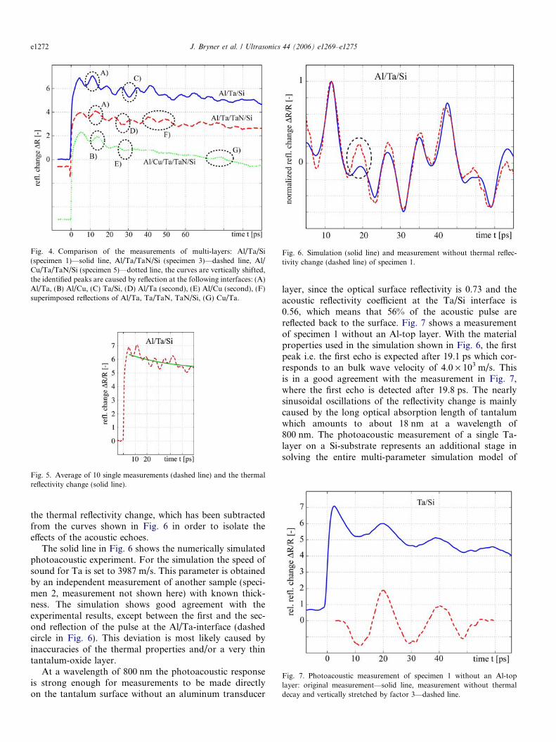
Fig. 4. Comparison of the measurements of multi-layers: Al/Ta/Si(specimen 1)—solid line, Al/Ta/TaN/Si (specimen 3)—dashed line, Al/Cu/Ta/TaN/Si (specimen 5)—dotted line, the curves are vertically shifted,the identified peaks are caused by reflection at the following interfaces: (A)Al/Ta, (B) Al/Cu, (C) Ta/Si, (D) Al/Ta (second), (E) Al/Cu (second), (F)superimposed reflections of Al/Ta, Ta/TaN, TaN/Si, (G) Cu/Ta.
Fig. 5. Average of 10 single measurements (dashed line) and the thermalreflectivity change (solid line).
Fig. 6. Simulation (solid line) and measurement without thermal reflec-tivity change (dashed line) of specimen 1.
Fig. 7. Photoacoustic measurement of specimen 1 without an Al-toplayer: original measurement—solid line, measurement without thermaldecay and vertically stretched by factor 3—dashed line.
e1272 J. Bryner et al. / Ultrasonics 44 (2006) e1269–e1275
the thermal reflectivity change, which has been subtractedfrom the curves shown in Fig. 6 in order to isolate theeffects of the acoustic echoes.
The solid line in Fig. 6 shows the numerically simulatedphotoacoustic experiment. For the simulation the speed ofsound for Ta is set to 3987 m/s. This parameter is obtainedby an independent measurement of another sample (speci-men 2, measurement not shown here) with known thick-ness. The simulation shows good agreement with theexperimental results, except between the first and the sec-ond reflection of the pulse at the Al/Ta-interface (dashedcircle in Fig. 6). This deviation is most likely caused byinaccuracies of the thermal properties and/or a very thintantalum-oxide layer.
At a wavelength of 800 nm the photoacoustic responseis strong enough for measurements to be made directlyon the tantalum surface without an aluminum transducer
layer, since the optical surface reflectivity is 0.73 and theacoustic reflectivity coefficient at the Ta/Si interface is0.56, which means that 56% of the acoustic pulse arereflected back to the surface. Fig. 7 shows a measurementof specimen 1 without an Al-top layer. With the materialproperties used in the simulation shown in Fig. 6, the firstpeak i.e. the first echo is expected after 19.1 ps which cor-responds to an bulk wave velocity of 4.0 · 103 m/s. Thisis in a good agreement with the measurement in Fig. 7,where the first echo is detected after 19.8 ps. The nearlysinusoidal oscillations of the reflectivity change is mainlycaused by the long optical absorption length of tantalumwhich amounts to about 18 nm at a wavelength of800 nm. The photoacoustic measurement of a single Ta-layer on a Si-substrate represents an additional stage insolving the entire multi-parameter simulation model of
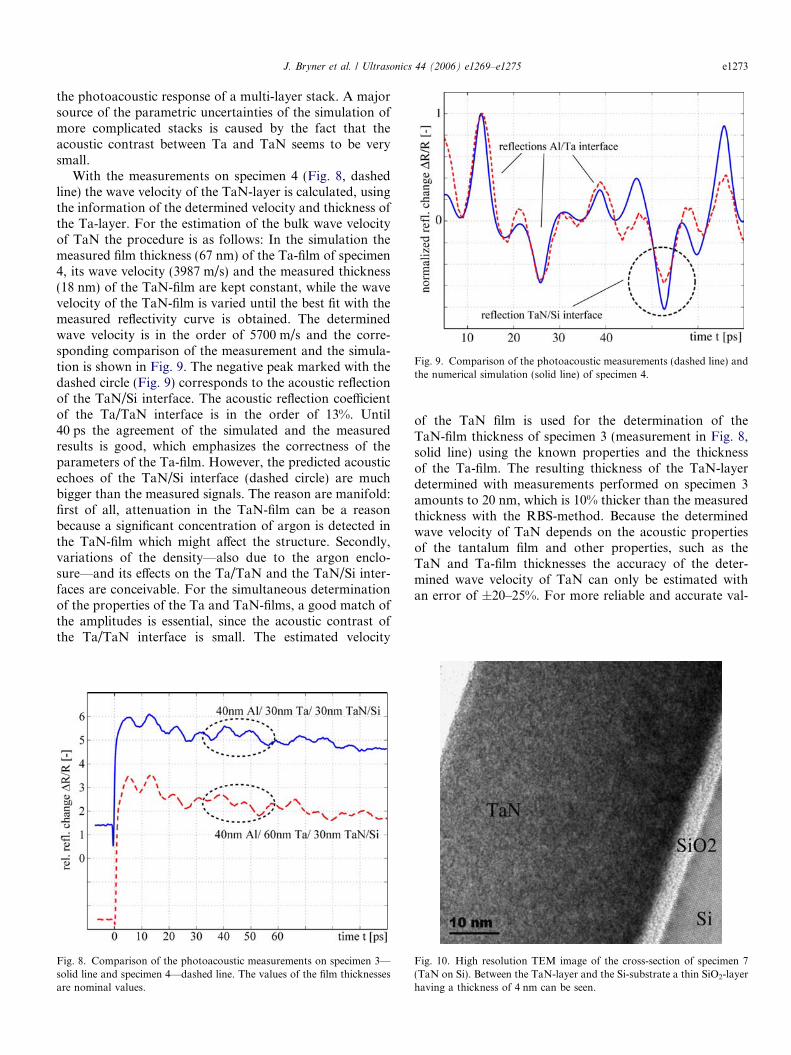
Fig. 9. Comparison of the photoacoustic measurements (dashed line) andthe numerical simulation (solid line) of specimen 4.
J. Bryner et al. / Ultrasonics 44 (2006) e1269–e1275 e1273
the photoacoustic response of a multi-layer stack. A majorsource of the parametric uncertainties of the simulation ofmore complicated stacks is caused by the fact that theacoustic contrast between Ta and TaN seems to be verysmall.
With the measurements on specimen 4 (Fig. 8, dashedline) the wave velocity of the TaN-layer is calculated, usingthe information of the determined velocity and thickness ofthe Ta-layer. For the estimation of the bulk wave velocityof TaN the procedure is as follows: In the simulation themeasured film thickness (67 nm) of the Ta-film of specimen4, its wave velocity (3987 m/s) and the measured thickness(18 nm) of the TaN-film are kept constant, while the wavevelocity of the TaN-film is varied until the best fit with themeasured reflectivity curve is obtained. The determinedwave velocity is in the order of 5700 m/s and the corre-sponding comparison of the measurement and the simula-tion is shown in Fig. 9. The negative peak marked with thedashed circle (Fig. 9) corresponds to the acoustic reflectionof the TaN/Si interface. The acoustic reflection coefficientof the Ta/TaN interface is in the order of 13%. Until40 ps the agreement of the simulated and the measuredresults is good, which emphasizes the correctness of theparameters of the Ta-film. However, the predicted acousticechoes of the TaN/Si interface (dashed circle) are muchbigger than the measured signals. The reason are manifold:first of all, attenuation in the TaN-film can be a reasonbecause a significant concentration of argon is detected inthe TaN-film which might affect the structure. Secondly,variations of the density—also due to the argon enclo-sure—and its effects on the Ta/TaN and the TaN/Si inter-faces are conceivable. For the simultaneous determinationof the properties of the Ta and TaN-films, a good match ofthe amplitudes is essential, since the acoustic contrast ofthe Ta/TaN interface is small. The estimated velocity
Fig. 8. Comparison of the photoacoustic measurements on specimen 3—solid line and specimen 4—dashed line. The values of the film thicknessesare nominal values.
of the TaN film is used for the determination of theTaN-film thickness of specimen 3 (measurement in Fig. 8,solid line) using the known properties and the thicknessof the Ta-film. The resulting thickness of the TaN-layerdetermined with measurements performed on specimen 3amounts to 20 nm, which is 10% thicker than the measuredthickness with the RBS-method. Because the determinedwave velocity of TaN depends on the acoustic propertiesof the tantalum film and other properties, such as theTaN and Ta-film thicknesses the accuracy of the deter-mined wave velocity of TaN can only be estimated withan error of ±20–25%. For more reliable and accurate val-
Fig. 10. High resolution TEM image of the cross-section of specimen 7(TaN on Si). Between the TaN-layer and the Si-substrate a thin SiO2-layerhaving a thickness of 4 nm can be seen.
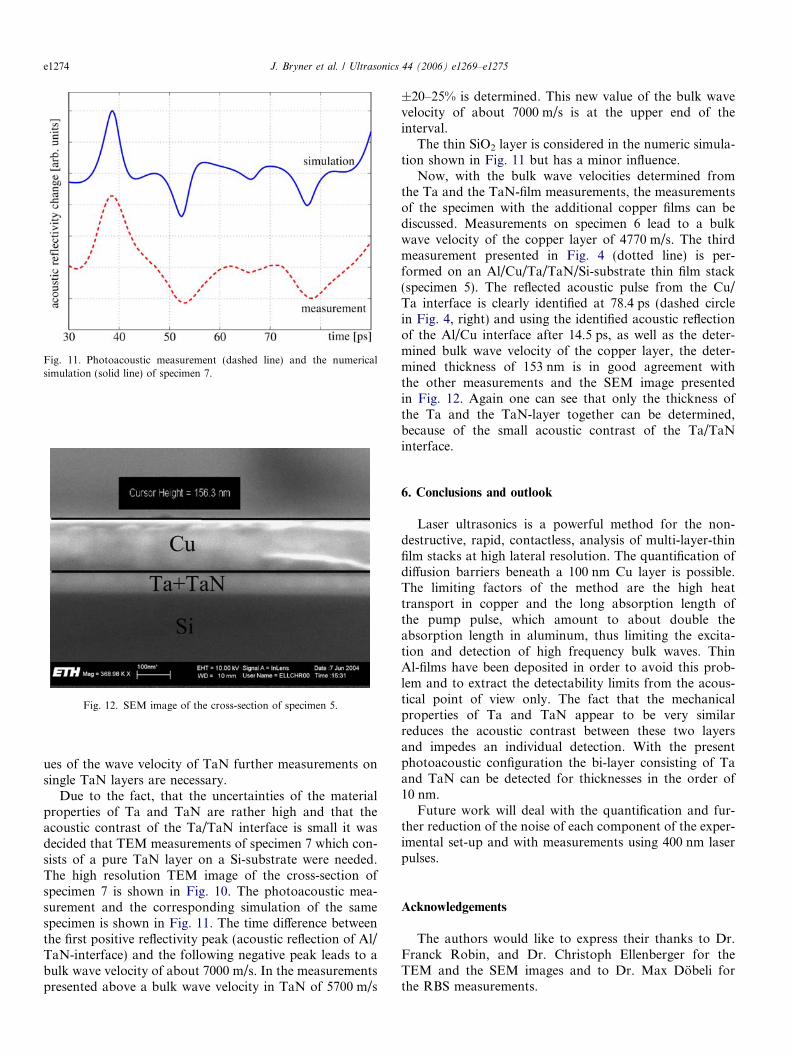
Fig. 11. Photoacoustic measurement (dashed line) and the numericalsimulation (solid line) of specimen 7.
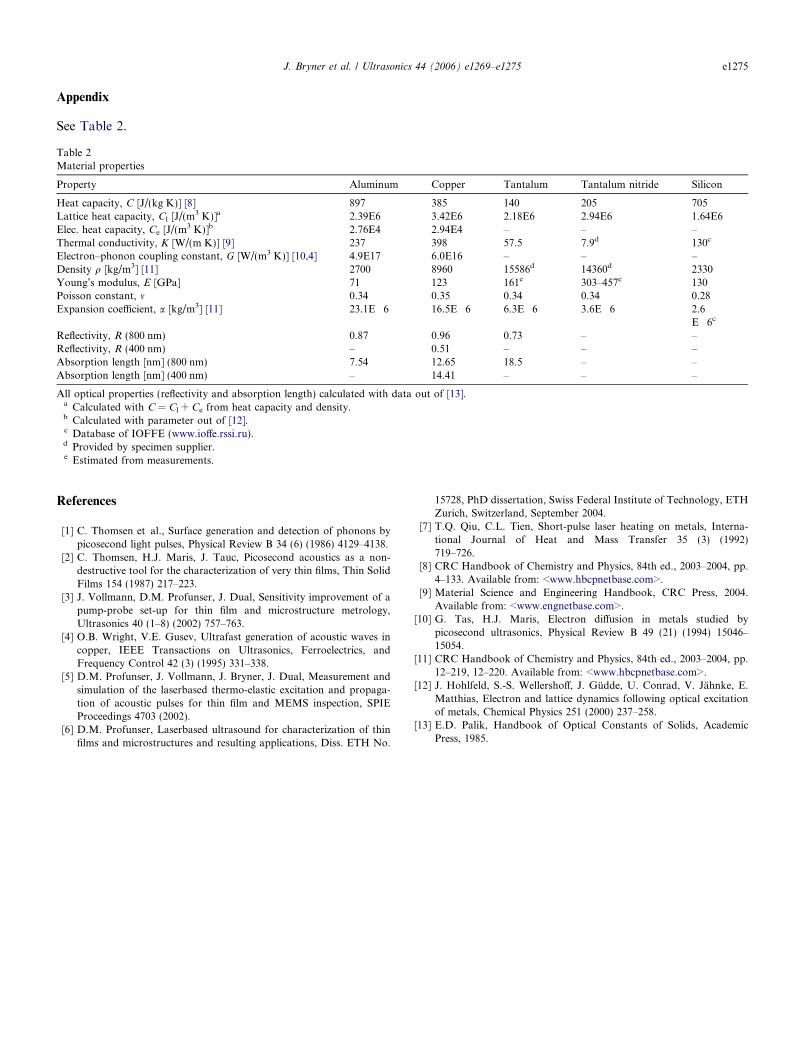
Fig. 12. SEM image of the cross-section of specimen 5.
e1274 J. Bryner et al. / Ultrasonics 44 (2006) e1269–e1275
ues of the wave velocity of TaN further measurements onsingle TaN layers are necessary.
Due to the fact, that the uncertainties of the materialproperties of Ta and TaN are rather high and that theacoustic contrast of the Ta/TaN interface is small it wasdecided that TEM measurements of specimen 7 which con-sists of a pure TaN layer on a Si-substrate were needed.The high resolution TEM image of the cross-section ofspecimen 7 is shown in Fig. 10. The photoacoustic mea-surement and the corresponding simulation of the samespecimen is shown in Fig. 11. The time difference betweenthe first positive reflectivity peak (acoustic reflection of Al/TaN-interface) and the following negative peak leads to abulk wave velocity of about 7000 m/s. In the measurementspresented above a bulk wave velocity in TaN of 5700 m/s
±20–25% is determined. This new value of the bulk wavevelocity of about 7000 m/s is at the upper end of theinterval.
The thin SiO2 layer is considered in the numeric simula-tion shown in Fig. 11 but has a minor influence.
Now, with the bulk wave velocities determined fromthe Ta and the TaN-film measurements, the measurementsof the specimen with the additional copper films can bediscussed. Measurements on specimen 6 lead to a bulkwave velocity of the copper layer of 4770 m/s. The thirdmeasurement presented in Fig. 4 (dotted line) is per-formed on an Al/Cu/Ta/TaN/Si-substrate thin film stack(specimen 5). The reflected acoustic pulse from the Cu/Ta interface is clearly identified at 78.4 ps (dashed circlein Fig. 4, right) and using the identified acoustic reflectionof the Al/Cu interface after 14.5 ps, as well as the deter-mined bulk wave velocity of the copper layer, the deter-mined thickness of 153 nm is in good agreement withthe other measurements and the SEM image presentedin Fig. 12. Again one can see that only the thickness ofthe Ta and the TaN-layer together can be determined,because of the small acoustic contrast of the Ta/TaNinterface.
6. Conclusions and outlook
Laser ultrasonics is a powerful method for the non-destructive, rapid, contactless, analysis of multi-layer-thinfilm stacks at high lateral resolution. The quantification ofdiffusion barriers beneath a 100 nm Cu layer is possible.The limiting factors of the method are the high heattransport in copper and the long absorption length ofthe pump pulse, which amount to about double theabsorption length in aluminum, thus limiting the excita-tion and detection of high frequency bulk waves. ThinAl-films have been deposited in order to avoid this prob-lem and to extract the detectability limits from the acous-tical point of view only. The fact that the mechanicalproperties of Ta and TaN appear to be very similarreduces the acoustic contrast between these two layersand impedes an individual detection. With the presentphotoacoustic configuration the bi-layer consisting of Taand TaN can be detected for thicknesses in the order of10 nm.
Future work will deal with the quantification and fur-ther reduction of the noise of each component of the exper-imental set-up and with measurements using 400 nm laserpulses.
Acknowledgements
The authors would like to express their thanks to Dr.Franck Robin, and Dr. Christoph Ellenberger for theTEM and the SEM images and to Dr. Max Dobeli forthe RBS measurements.
J. Bryner et al. / Ultrasonics 44 (2006) e1269–e1275 e1275
Appendix
See Table 2.
Table 2Material properties
Property Aluminum Copper Tantalum Tantalum nitride Silicon
Heat capacity, C [J/(kg K)] [8] 897 385 140 205 705Lattice heat capacity, Cl [J/(m3 K)]a 2.39E6 3.42E6 2.18E6 2.94E6 1.64E6Elec. heat capacity, Ce [J/(m3 K)]b 2.76E4 2.94E4 – – –Thermal conductivity, K [W/(m K)] [9] 237 398 57.5 7.9d 130c
Electron–phonon coupling constant, G [W/(m3 K)] [10,4] 4.9E17 6.0E16 – – –Density q [kg/m3] [11] 2700 8960 15586d 14360d 2330Young’s modulus, E [GPa] 71 123 161e 303–457e 130Poisson constant, m 0.34 0.35 0.34 0.34 0.28Expansion coefficient, a [kg/m3] [11] 23.1E�6 16.5E�6 6.3E�6 3.6E�6 2.6
E�6c
Reflectivity, R (800 nm) 0.87 0.96 0.73 – –Reflectivity, R (400 nm) – 0.51 – – –Absorption length [nm] (800 nm) 7.54 12.65 18.5 – –Absorption length [nm] (400 nm) – 14.41 – – –
All optical properties (reflectivity and absorption length) calculated with data out of [13].a Calculated with C = Cl + Ce from heat capacity and density.b Calculated with parameter out of [12].c Database of IOFFE (www.ioffe.rssi.ru).d Provided by specimen supplier.e Estimated from measurements.
References
[1] C. Thomsen et al., Surface generation and detection of phonons bypicosecond light pulses, Physical Review B 34 (6) (1986) 4129–4138.
[2] C. Thomsen, H.J. Maris, J. Tauc, Picosecond acoustics as a non-destructive tool for the characterization of very thin films, Thin SolidFilms 154 (1987) 217–223.
[3] J. Vollmann, D.M. Profunser, J. Dual, Sensitivity improvement of apump-probe set-up for thin film and microstructure metrology,Ultrasonics 40 (1–8) (2002) 757–763.
[4] O.B. Wright, V.E. Gusev, Ultrafast generation of acoustic waves incopper, IEEE Transactions on Ultrasonics, Ferroelectrics, andFrequency Control 42 (3) (1995) 331–338.
[5] D.M. Profunser, J. Vollmann, J. Bryner, J. Dual, Measurement andsimulation of the laserbased thermo-elastic excitation and propaga-tion of acoustic pulses for thin film and MEMS inspection, SPIEProceedings 4703 (2002).
[6] D.M. Profunser, Laserbased ultrasound for characterization of thinfilms and microstructures and resulting applications, Diss. ETH No.
15728, PhD dissertation, Swiss Federal Institute of Technology, ETHZurich, Switzerland, September 2004.
[7] T.Q. Qiu, C.L. Tien, Short-pulse laser heating on metals, Interna-tional Journal of Heat and Mass Transfer 35 (3) (1992)719–726.
[8] CRC Handbook of Chemistry and Physics, 84th ed., 2003–2004, pp.4–133. Available from: <www.hbcpnetbase.com>.
[9] Material Science and Engineering Handbook, CRC Press, 2004.Available from: <www.engnetbase.com>.
[10] G. Tas, H.J. Maris, Electron diffusion in metals studied bypicosecond ultrasonics, Physical Review B 49 (21) (1994) 15046–15054.
[11] CRC Handbook of Chemistry and Physics, 84th ed., 2003–2004, pp.12–219, 12–220. Available from: <www.hbcpnetbase.com>.
[12] J. Hohlfeld, S.-S. Wellershoff, J. Gudde, U. Conrad, V. Jahnke, E.Matthias, Electron and lattice dynamics following optical excitationof metals, Chemical Physics 251 (2000) 237–258.
[13] E.D. Palik, Handbook of Optical Constants of Solids, AcademicPress, 1985.


![The Story of Picosecond Ultrasonicsperso.univ-lemans.fr/~pruello/Picosecond ultrasonics from lab to... · The Story of Picosecond Ultrasonics 1 Christopher Morath, ... [ps] 0.00 0.05](https://img.pdfslide.us/doc/110x75/5a8820a97f8b9aa5408e58d4/the-story-of-picosecond-pruellopicosecond-ultrasonics-from-lab-tothe-story-of.jpg)