Embed Size (px)
Citation preview
1
Abstract—A micromachined on-wafer probe has been designed
to facilitate the development of integrated circuits in the 600 – 900 GHz frequency range. The probe tip is fabricated on a 5-micrometer thick high-resistivity silicon substrate using a silicon-on-insulator fabrication process. This letter updates previous work on WR-1.2 wafer probes and presents for the first time the full RF characterization of the probe. These are the first reported on-wafer measurements above 750 GHz.
Index Terms—Micromachining, probes, submillimeter wave integrated circuits, submillimeter wave measurements.
I. INTRODUCTION HE TERAHERTZ frequency spectrum is a potential tool for many applications [1] and recent advances [2]-[4] in
the development of terahertz monolithic integrated circuits (TMICs) promise to unlock this potential. The development of TMICs relies on accurate device models, which are most readily and accurately obtained through on-wafer probing [5]. Without on-wafer measurement infrastructure, researchers must use alternative testing methods that involve dicing out individual circuits to mount in a test fixture, which is inherently time consuming and introduces additional uncertainty associated with the waveguide housing. To address the relative lack of terahertz on-wafer measurement infrastructure, the University of Virginia developed a WR-1.5 micromachined probe [6], [7], which for the first time enabled on-wafer measurements up to 750 GHz [2]. While WR-1.5 wafer probes are now commercially available [8], higher frequency on-wafer probes are needed to facilitate the development of TMICs operating above 750 GHz. In [9], we presented initial test results (up to 750 GHz) of a micromachined probe for the WR-1.2 waveguide band (600 – 900 GHz). This letter updates that work and presents the full
Manuscript received March 18, 2014; revised May 19, 2014; accepted May
19, 2014. This work was supported by the U.S. Army National Ground Intelligence Center (NGIC) under contract W911W5-11-C-0013, the Defense Advanced Research Projects Agency (DARPA) Terahertz (THz) Electronics Program and Army Research Laboratory (ARL) under DARPA Contract no. HR0011-09-C-0062 under a sub-contract from Northrop Grumman, and the Army Research Office (ARO) and Dominion MicroProbes, Inc. (DMPI) through STTR contract W911NF-13-C-0010.
The authors are with the Charles L. Brown Department of Electrical and Computer Engineering, University of Virginia, Charlottesville, VA, 22904-4743, USA (e-mail: [email protected]; [email protected]).
characterization of the WR-1.2 probe, including the first reported on-wafer measurements up to 900 GHz.
II. PROBE CONCEPT & DESIGN The WR-1.2 micromachined probe assembly, shown in Fig.
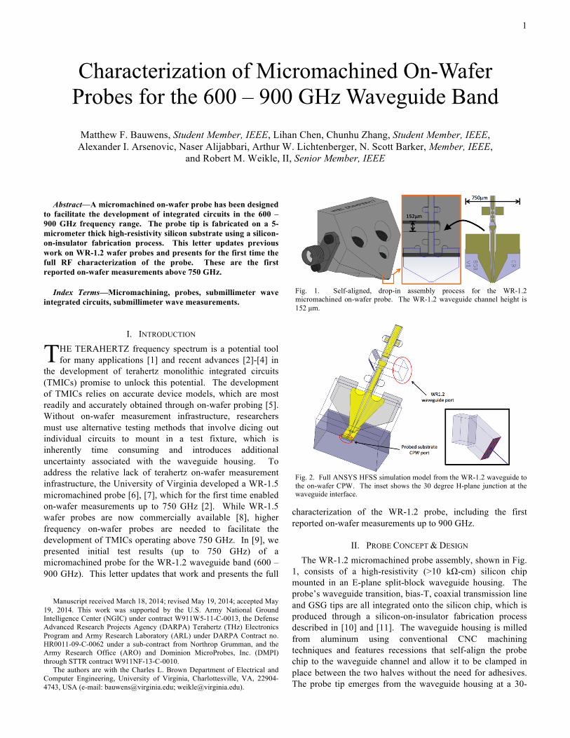
1, consists of a high-resistivity (>10 kΩ-cm) silicon chip mounted in an E-plane split-block waveguide housing. The probe’s waveguide transition, bias-T, coaxial transmission line and GSG tips are all integrated onto the silicon chip, which is produced through a silicon-on-insulator fabrication process described in [10] and [11]. The waveguide housing is milled from aluminum using conventional CNC machining techniques and features recessions that self-align the probe chip to the waveguide channel and allow it to be clamped in place between the two halves without the need for adhesives. The probe tip emerges from the waveguide housing at a 30-
Characterization of Micromachined On-Wafer Probes for the 600 – 900 GHz Waveguide Band
Matthew F. Bauwens, Student Member, IEEE, Lihan Chen, Chunhu Zhang, Student Member, IEEE, Alexander I. Arsenovic, Naser Alijabbari, Arthur W. Lichtenberger, N. Scott Barker, Member, IEEE,
and Robert M. Weikle, II, Senior Member, IEEE
T
Fig. 1. Self-aligned, drop-in assembly process for the WR-1.2 micromachined on-wafer probe. The WR-1.2 waveguide channel height is 152 µm.
Fig. 2. Full ANSYS HFSS simulation model from the WR-1.2 waveguide to the on-wafer CPW. The inset shows the 30 degree H-plane junction at the waveguide interface.
2
degree angle, allowing the GSG tips to extend below the waveguide housing to contact the device under test.
The electromagnetic design of the probe consists of two transitions, one from WR-1.2 rectangular waveguide to a substrate-supported rectangular coaxial transmission line, and a second from the rectangular coaxial transmission line to coplanar waveguide (CPW), which extends down to the tips. To prevent excitation of higher order modes in the rectangular coaxial channel, the silicon substrate thickness is chosen to be 5 µm [9]. These transitions are optimized in ANSYS HFSS to maximize the waveguide and CPW return loss. In the simulation model, shown in Fig. 2, the probe chip metallization is cobalt-hardened gold, with conductivity of 1.1x10⁷ Siemens per meter (S/m), the on-wafer CPW is soft gold with a conductivity of 3.2x10⁷ S/m and the waveguide channel walls are aluminum with a conductivity of 2.7x10⁷ S/m and a surface roughness of 100 nm based on the RMS value obtained from a Veeco NT1100 optical profilometer. Shown in the Fig. 2 inset is the 30-degree H-plane waveguide junction in which the waveguide port representing the probe is de-embedded by 20.3 mm. This structure captures the loss of the waveguide between the WR-1.2 interface and the
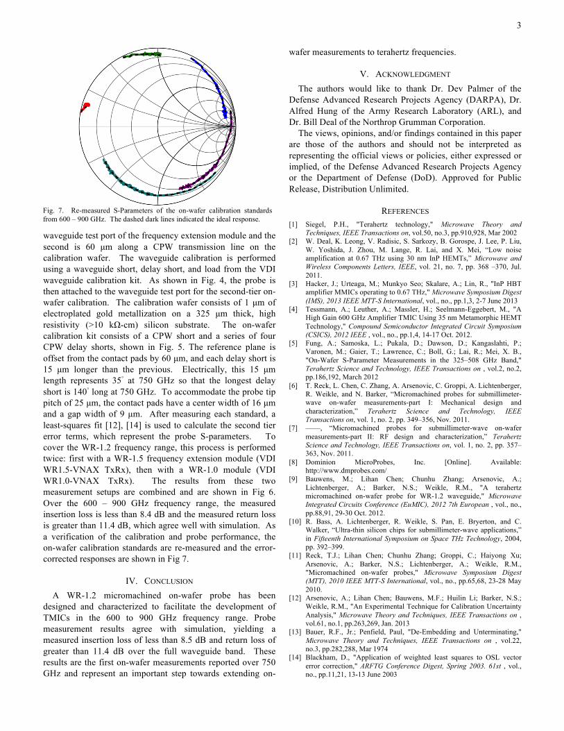
waveguide transition as well as the mismatch of the 30-degree junction. This simulation is combined with that of the probe to produce the predicted probe S-parameters, shown in Fig. 3. The simulated insertion loss is less than 10.0 dB and the simulated return loss is greater than 11.8 dB over the WR-1.2 band. At 750 GHz, the 6.7 dB of simulated loss breaks down as follows: (1) 3.8 dB from the 20.3 mm WR-1.2 waveguide, (2) 0.3 dB from the rectangular waveguide to rectangular coaxial transition, and (3) 2.6 dB from the rectangular coax to the on-wafer CPW. Not shown is the bias port isolation, which is greater than 20 dB over the WR-1.2 band.
III. RF CHARACTERIZATION The University of Virginia does not have a WR-1.2
frequency extension module. To test the WR-1.2 probe, measurements are performed in the WR-1.5 and WR-1.0 waveguide bands. According to simulation, the return loss due to the resulting mismatch at the probe’s waveguide input is less than 22 dB across the WR-1.2 band. This effect is included in both measured and simulated data. The one-port S-parameter test setup consists of a Virginia Diodes, Inc. (VDI) vector network analyzer extension module connected to an Agilent PNA-X (N5245A) network analyzer. By utilizing a two-tier calibration technique [12], [13], the full two-port S-parameters of the probe are determined. This method consists of performing calibrations at the two reference planes of interest. In this case, the first reference plane is at the
Fig. 6. De-embedded probe S-parameters combined from the WR-1.5 and WR-1.0 calibrations. The vertical bars indicate the WR-1.2 frequency band edges. The calibrations are combined at 780 GHz, resulting in a discontinuity at that frequency point.
Fig. 5. The on-wafer calibration kit features a CPW short and four CPW delay shorts. The reference plane is offset from the pads by 60 µm.
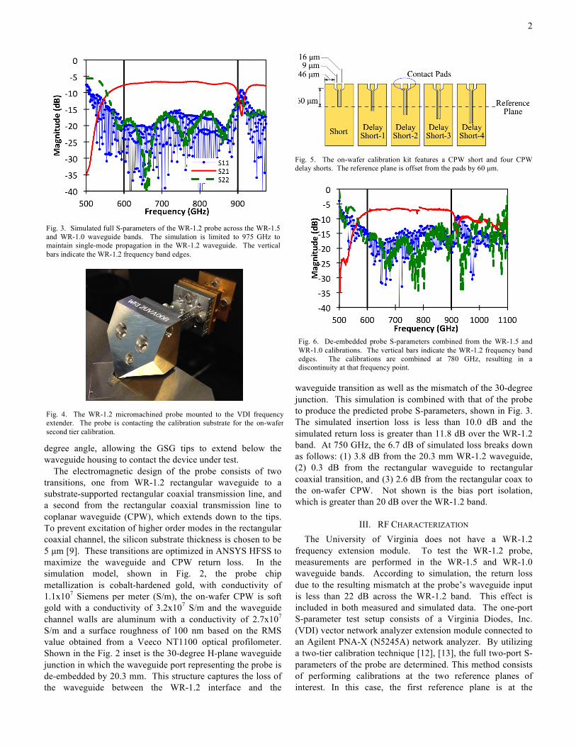
Fig. 4. The WR-1.2 micromachined probe mounted to the VDI frequency extender. The probe is contacting the calibration substrate for the on-wafer second tier calibration.
Fig. 3. Simulated full S-parameters of the WR-1.2 probe across the WR-1.5 and WR-1.0 waveguide bands. The simulation is limited to 975 GHz to maintain single-mode propagation in the WR-1.2 waveguide. The vertical bars indicate the WR-1.2 frequency band edges.
3
waveguide test port of the frequency extension module and the second is 60 µm along a CPW transmission line on the calibration wafer. The waveguide calibration is performed using a waveguide short, delay short, and load from the VDI waveguide calibration kit. As shown in Fig. 4, the probe is then attached to the waveguide test port for the second-tier on-wafer calibration. The calibration wafer consists of 1 µm of electroplated gold metallization on a 325 µm thick, high resistivity (>10 kΩ-cm) silicon substrate. The on-wafer calibration kit consists of a CPW short and a series of four CPW delay shorts, shown in Fig. 5. The reference plane is offset from the contact pads by 60 µm, and each delay short is 15 µm longer than the previous. Electrically, this 15 µm length represents 35◦ at 750 GHz so that the longest delay short is 140◦ long at 750 GHz. To accommodate the probe tip pitch of 25 µm, the contact pads have a center width of 16 µm and a gap width of 9 µm. After measuring each standard, a least-squares fit [12], [14] is used to calculate the second tier error terms, which represent the probe S-parameters. To cover the WR-1.2 frequency range, this process is performed twice: first with a WR-1.5 frequency extension module (VDI WR1.5-VNAX TxRx), then with a WR-1.0 module (VDI WR1.0-VNAX TxRx). The results from these two measurement setups are combined and are shown in Fig 6. Over the 600 – 900 GHz frequency range, the measured insertion loss is less than 8.4 dB and the measured return loss is greater than 11.4 dB, which agree well with simulation. As a verification of the calibration and probe performance, the on-wafer calibration standards are re-measured and the error-corrected responses are shown in Fig 7.
IV. CONCLUSION A WR-1.2 micromachined on-wafer probe has been
designed and characterized to facilitate the development of TMICs in the 600 to 900 GHz frequency range. Probe measurement results agree with simulation, yielding a measured insertion loss of less than 8.5 dB and return loss of greater than 11.4 dB over the full waveguide band. These results are the first on-wafer measurements reported over 750 GHz and represent an important step towards extending on-
wafer measurements to terahertz frequencies.
V. ACKNOWLEDGMENT The authors would like to thank Dr. Dev Palmer of the
Defense Advanced Research Projects Agency (DARPA), Dr. Alfred Hung of the Army Research Laboratory (ARL), and Dr. Bill Deal of the Northrop Grumman Corporation.
The views, opinions, and/or findings contained in this paper are those of the authors and should not be interpreted as representing the official views or policies, either expressed or implied, of the Defense Advanced Research Projects Agency or the Department of Defense (DoD). Approved for Public Release, Distribution Unlimited.
REFERENCES [1] Siegel, P.H., "Terahertz technology," Microwave Theory and
Techniques, IEEE Transactions on, vol.50, no.3, pp.910,928, Mar 2002 [2] W. Deal, K. Leong, V. Radisic, S. Sarkozy, B. Gorospe, J. Lee, P. Liu,
W. Yoshida, J. Zhou, M. Lange, R. Lai, and X. Mei, “Low noise amplification at 0.67 THz using 30 nm InP HEMTs,” Microwave and Wireless Components Letters, IEEE, vol. 21, no. 7, pp. 368 –370, Jul. 2011.
[3] Hacker, J.; Urteaga, M.; Munkyo Seo; Skalare, A.; Lin, R., "InP HBT amplifier MMICs operating to 0.67 THz," Microwave Symposium Digest (IMS), 2013 IEEE MTT-S International, vol., no., pp.1,3, 2-7 June 2013
[4] Tessmann, A.; Leuther, A.; Massler, H.; Seelmann-Eggebert, M., "A High Gain 600 GHz Amplifier TMIC Using 35 nm Metamorphic HEMT Technology," Compound Semiconductor Integrated Circuit Symposium (CSICS), 2012 IEEE , vol., no., pp.1,4, 14-17 Oct. 2012.
[5] Fung, A.; Samoska, L.; Pukala, D.; Dawson, D.; Kangaslahti, P.; Varonen, M.; Gaier, T.; Lawrence, C.; Boll, G.; Lai, R.; Mei, X. B., "On-Wafer S-Parameter Measurements in the 325–508 GHz Band," Terahertz Science and Technology, IEEE Transactions on , vol.2, no.2, pp.186,192, March 2012
[6] T. Reck, L. Chen, C. Zhang, A. Arsenovic, C. Groppi, A. Lichtenberger, R. Weikle, and N. Barker, “Micromachined probes for submillimeter-wave on-wafer measurements-part I: Mechanical design and characterization,” Terahertz Science and Technology, IEEE Transactions on, vol. 1, no. 2, pp. 349–356, Nov. 2011.
[7] ——, “Micromachined probes for submillimeter-wave on-wafer measurements-part II: RF design and characterization,” Terahertz Science and Technology, IEEE Transactions on, vol. 1, no. 2, pp. 357–363, Nov. 2011.
[8] Dominion MicroProbes, Inc. [Online]. Available: http://www.dmprobes.com/
[9] Bauwens, M.; Lihan Chen; Chunhu Zhang; Arsenovic, A.; Lichtenberger, A.; Barker, N.S.; Weikle, R.M., "A terahertz micromachined on-wafer probe for WR-1.2 waveguide," Microwave Integrated Circuits Conference (EuMIC), 2012 7th European , vol., no., pp.88,91, 29-30 Oct. 2012.
[10] R. Bass, A. Lichtenberger, R. Weikle, S. Pan, E. Bryerton, and C. Walker, “Ultra-thin silicon chips for submillimeter-wave applications,” in Fifteenth International Symposium on Space THz Technology, 2004, pp. 392–399.
[11] Reck, T.J.; Lihan Chen; Chunhu Zhang; Groppi, C.; Haiyong Xu; Arsenovic, A.; Barker, N.S.; Lichtenberger, A.; Weikle, R.M., "Micromachined on-wafer probes," Microwave Symposium Digest (MTT), 2010 IEEE MTT-S International, vol., no., pp.65,68, 23-28 May 2010.
[12] Arsenovic, A.; Lihan Chen; Bauwens, M.F.; Huilin Li; Barker, N.S.; Weikle, R.M., "An Experimental Technique for Calibration Uncertainty Analysis," Microwave Theory and Techniques, IEEE Transactions on , vol.61, no.1, pp.263,269, Jan. 2013
[13] Bauer, R.F., Jr.; Penfield, Paul, "De-Embedding and Unterminating," Microwave Theory and Techniques, IEEE Transactions on , vol.22, no.3, pp.282,288, Mar 1974
[14] Blackham, D., "Application of weighted least squares to OSL vector error correction," ARFTG Conference Digest, Spring 2003. 61st , vol., no., pp.11,21, 13-13 June 2003
Fig. 7. Re-measured S-Parameters of the on-wafer calibration standards from 600 – 900 GHz. The dashed dark lines indicated the ideal response.