Embed Size (px)
Citation preview

University of Bologna
School of Engineering and Architecture
Telecommunications Engineering
Communication Networks, Systems and Services (CN2S)
Associated with the School of Engineering
In University of Glasgow, Scotland, UK
Characterization of integrated Bragg gratings in silicon-
on-insulator
A Master Degree Thesis By:
Aktham Tashtush.
Rapporteur :
Prof. Paolo Bassi.
Supervisors:
Dr.Marc Sorel.
Piero Orlandi.

Abstract
Silicon-on-insulator (SOI) is rapidly emerging as a very promising material platform for integrated
photonics.
As it combines the potential for optoelectronic integration with the low-cost and large volume
manufacturing capabilities and they are already accumulate a huge amount of applications in areas
like sensing, quantum optics, optical telecommunications and metrology.
One of the main limitations of current technology is that waveguide propagation losses are still much
higher than in standard glass-based platform because of many reasons such as bends, surface
roughness and the very strong optical confinement provided by SOI.
Such high loss prevents the fabrication of efficient optical resonators and complex devices severely
limiting the current potential of the SOI platform.
The project in the first part deals with the simple waveguides loss problem and trying to link that with
the polarization problem and the loss based on Fabry-Perot Technique.
The second part of the thesis deals with the Bragg Grating characterization from again the point of
view of the polarization effect which leads to a better stop-band use filters.
To a better comprehension a brief review on the basics of the SOI and the integrated Bragg grating
ends up with the fabrication techniques and some of its applications will be presented in both parts,
until the end of both the third and the fourth chapters to some results which hopefully make its
precedent explanations easier to deal with.

Acknowledgment
الحمد هلل حمداً كثيراً
First I would like to thank my parents who never stopped supporting me no matter what and where
ever I‘m at, as much as human being should love and appreciate their parents I shall always be the
one who‘s doing it much more.
A great thanks and appreciation to my supervisor Prof.Paolo Bassi who was so initiative, stepped up
and approached like nearly no Professor would do and offered this whole idea on me ,being more
excited than I for having me on his small team in this small project so I will be so grateful for what he
did as there‘s a beat in my heart. Also to my supervisor in University of Glasgow Dr.Marc Sorel for his
guidance and patience of course well !! because as much as bright I was, I wasn‘t that great so
whenever he was needed he was just a minute from popping right in, To Michael Strain for his sample
that I used and for his really a great help in the lab and last but not least To Piero Orlandi for helping
me in the first couple of weeks to acclimate in the Laboratory in Glasgow and get used to my new set-
ups.
And as they say ―self-commendation makes you keep going‖, so, to myself for being courageous,
understanding and hard worker, hopping this wouldn‘t be the end but the start.
Well done all, well done me, And God Bless.
Contents
Abstract -2
Acknowledgment -1
Contents ….. 0
Chapter 1: Optical Waveguides Fundamentals
1.1 Definitions 2
1.2 Ray-Optic Approach 3
1.3 Transvers Modes 4
1.3.1 Modes of Propagation 5
1.4 Conclusion 8
Chapter 2: A Glimpse on the Silicon on Insulator
2.1 What is SOI Technology? 9
2.2 SOI wafers fabrication 11
2.2.1 The Fabrication Technique 11
2.2.2 Smart Cut 14
2.3 SOI Applications 15
2.4 Conclusion 16
Chapter 3: Waveguides Losses
3.1 Attenuation Coefficient 18
3.1.1 Definition and Formula 19
3.2 Losses In Waveguides 19
3.2.1 Scattering Losses 19
3.2.2 Absorption Losses 20
3.2.2.1 Interband Absorption 20
3.2.2.2 Free Carrier Absorption 21
3.2.3 Radiation Losses in optical waveguides 22
3.3 Measurement of propagation loss in optical waveguides 22
3.3.1 Using Fabry-Perot Resonance Method 23
3.4 Experimental Set-Up 27
3.4.1 Used Device Characterization 29
3.4.2 Results and Discussion 30
3.5 Conclusion 33
Chapter 4: Bragg Grating
4.1 What‘s a Bragg Grating 34
4.2 Integrated Bragg Grating Fabrication Techniques 37
4.2.1 Lithography 37
4.2.1.1 Photolithography 37
4.2.1.2 Electron-beam lithography 38
4.2.2 E-beam resists and reactive ion etching 38
4.3 Experimental Set-up 42
4.3.1 Used Device Characterization 42
4.3.2 Results and Discussion 42
4.4 Conclusion 51
References 53
Figures and Tables List 60
Chapter 1
Optical Waveguides Fundamentals
In this first chapter the reader will get to know the definition of the optical waveguide then a quick
review for the Maxwell‘s and the wave equation and the basic model which all optics relies on the ray
model where the light behavior inside a waveguide can be realized all will be presented.
Then a better look on the Transvers Modes that travels in the medium will be reviewed in which a
close look on the differences between each other can be understood, and that will prepare the reader
to have a good start on the waveguide and polarization effect relation on the next chapters.
1.1 Definitions
The optical waveguide is the fundamental element that interconnects the various devices of an optical
integrated circuit, just as a metallic strip does in an electrical integrated circuit. However, unlike
electrical current that flows through a metal strip according to Ohm‘s law, optical waves travel in the
waveguide in distinct optical modes. [1]
A mode is the field spatial distribution which solves Maxwell's equations in a longitudinally constant
structure. It transversal shape is constant. Along the propagation distance it has an exponential
dependence on attenuation and propagation constants. In general, Maxwell's equations are solved in
harmonic regime, where there‘s no time dependence.
The plane wave is the most fundamental electromagnetic wave and it is a particular solution of
Maxwell‘s equations. It will be used to develop the fundamentals of electromagnetic waves in dielectric
media including solutions to Maxwell‘s equations, phase velocity, group velocity, polarization,
boundary conditions, and total internal reflection, which makes it possible for optical signals to
propagate and be guided in waveguides. [2]
So here‘s a quick mentioning for the Maxwell‘s equations:
(1.1)
(1.2)
(1.3)
(1.4)
Where E is the electric field vector, B the magnetic flux density vector, D the electric flux density or
electric displacement vector, and H the magnetic field vector. The parameter ρ is the volume density
of free charge, and J is the density vector of free currents.
The flux densities D and B are related to the fields E and H by the constitutive relations. For linear,
isotropic media, the relations are given by D =ε E and B =μ H, where ε is the dielectric permittivity of
the medium and μ is the magnetic permeability of the medium. A dielectric medium is linear if the
permittivity ε and permeability μ are independent of field strengths. [2]
The solutions to the wave equations with a given frequency in the form of [2]:
(1.5)
And
(1.6)
And by using (1.5) and (1.6) the wave equation for E reduced to:
(1.7)
Noting that:
(1.8)
And
(1.9)
With 0
All of the above formulas will be used on the boundaries of the planes by the applying the boundary
conditions and at this level it won‘t be mentioned excessively here but it can be reviewed on
Reference no. [3] and the first chapter of Reference no. [2].
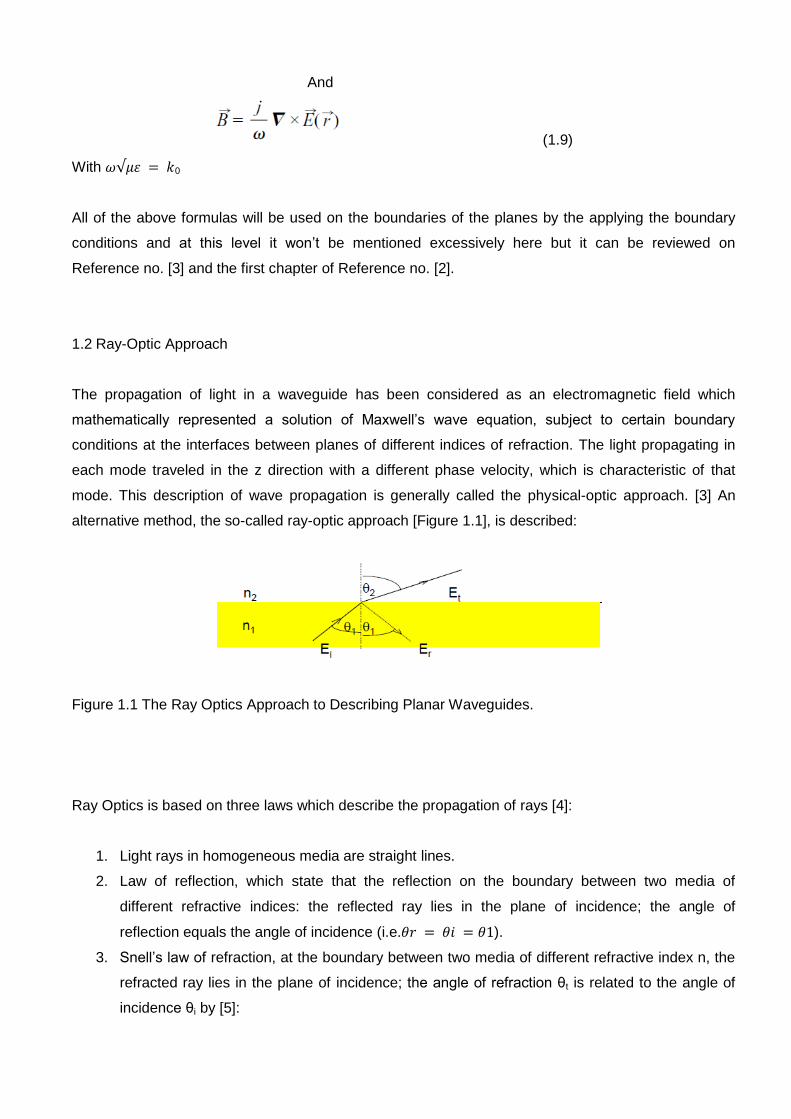
1.2 Ray-Optic Approach
The propagation of light in a waveguide has been considered as an electromagnetic field which
mathematically represented a solution of Maxwell‘s wave equation, subject to certain boundary
conditions at the interfaces between planes of different indices of refraction. The light propagating in
each mode traveled in the z direction with a different phase velocity, which is characteristic of that
mode. This description of wave propagation is generally called the physical-optic approach. [3] An
alternative method, the so-called ray-optic approach [Figure 1.1], is described:
Figure 1.1 The Ray Optics Approach to Describing Planar Waveguides.
Ray Optics is based on three laws which describe the propagation of rays [4]:
1. Light rays in homogeneous media are straight lines.
2. Law of reflection, which state that the reflection on the boundary between two media of
different refractive indices: the reflected ray lies in the plane of incidence; the angle of
reflection equals the angle of incidence (i.e. ).
3. Snell‘s law of refraction, at the boundary between two media of different refractive index n, the
refracted ray lies in the plane of incidence; the angle of refraction θt is related to the angle of
incidence θi by [5]:
(1.10)
The lightwave becomes totally confined, as shown in Fig. 1.1, corresponding to a guided mode. In this
case, the critical angle is given by
(1.11)
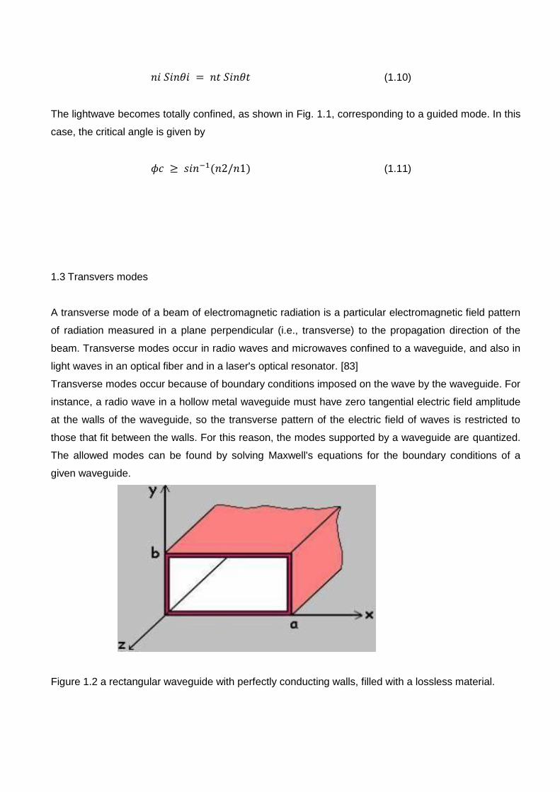
1.3 Transvers modes
A transverse mode of a beam of electromagnetic radiation is a particular electromagnetic field pattern
of radiation measured in a plane perpendicular (i.e., transverse) to the propagation direction of the
beam. Transverse modes occur in radio waves and microwaves confined to a waveguide, and also in
light waves in an optical fiber and in a laser's optical resonator. [83]
Transverse modes occur because of boundary conditions imposed on the wave by the waveguide. For
instance, a radio wave in a hollow metal waveguide must have zero tangential electric field amplitude
at the walls of the waveguide, so the transverse pattern of the electric field of waves is restricted to
those that fit between the walls. For this reason, the modes supported by a waveguide are quantized.
The allowed modes can be found by solving Maxwell's equations for the boundary conditions of a
given waveguide.
Figure 1.2 a rectangular waveguide with perfectly conducting walls, filled with a lossless material.
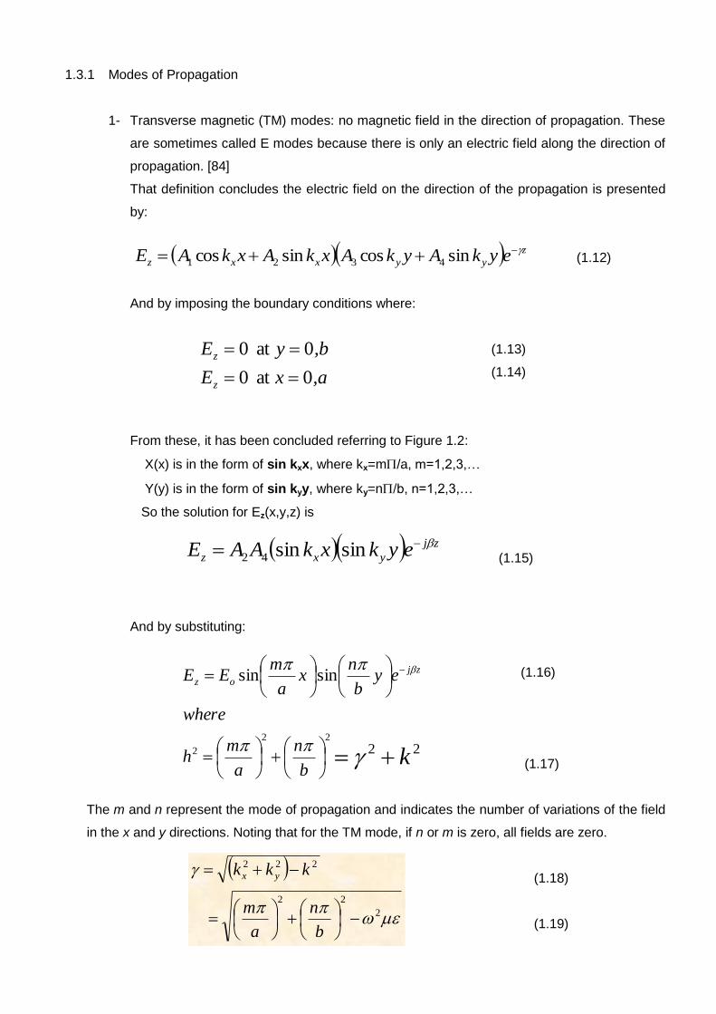
1.3.1 Modes of Propagation
1- Transverse magnetic (TM) modes: no magnetic field in the direction of propagation. These
are sometimes called E modes because there is only an electric field along the direction of
propagation. [84]
That definition concludes the electric field on the direction of the propagation is presented
by:
(1.12)
And by imposing the boundary conditions where:
(1.13)
(1.14)
From these, it has been concluded referring to Figure 1.2:
X(x) is in the form of sin kxx, where kx=m/a, m=1,2,3,…
Y(y) is in the form of sin kyy, where ky=n/b, n=1,2,3,…
So the solution for Ez(x,y,z) is
(1.15)
And by substituting:
(1.16)
(1.17)
The m and n represent the mode of propagation and indicates the number of variations of the field
in the x and y directions. Noting that for the TM mode, if n or m is zero, all fields are zero.
(1.18)
(1.19)
z
yyxxz eykAykAxkAxkAE sincossincos 4321
,axE
,byE
z
z
0at 0
0at 0
zj
yxz eykxkAAE sinsin42
22
2
sinsin
b
n
a
mh
where
eyb
nx
a
mEE zj
oz
22 k
2
22
222
b
n
a
m
kkk yx
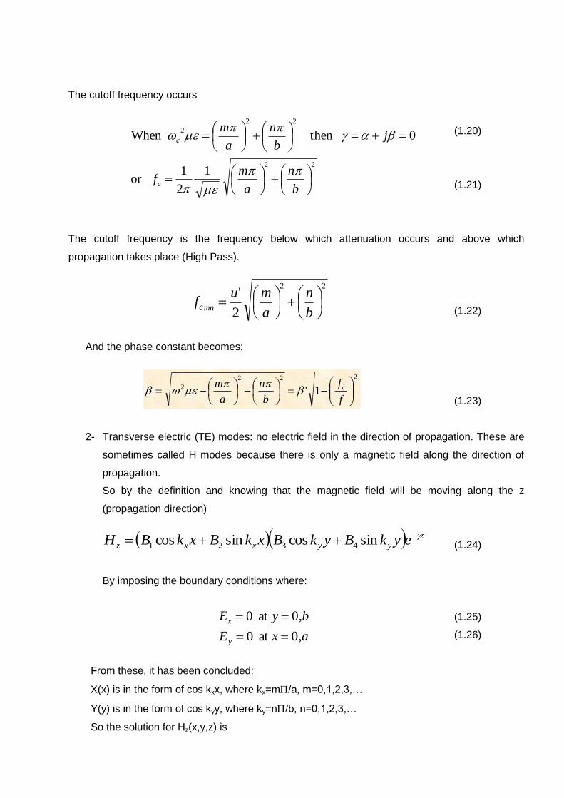
The cutoff frequency occurs
(1.20)
(1.21)
The cutoff frequency is the frequency below which attenuation occurs and above which
propagation takes place (High Pass).
(1.22)
And the phase constant becomes:
(1.23)
2- Transverse electric (TE) modes: no electric field in the direction of propagation. These are
sometimes called H modes because there is only a magnetic field along the direction of
propagation.
So by the definition and knowing that the magnetic field will be moving along the z
(propagation direction)
(1.24)
By imposing the boundary conditions where:
(1.25)
(1.26)
From these, it has been concluded:
X(x) is in the form of cos kxx, where kx=m/a, m=0,1,2,3,…
Y(y) is in the form of cos kyy, where ky=n/b, n=0,1,2,3,…
So the solution for Hz(x,y,z) is
,axE
,byE
y
x
0at 0
0at 0
z
yyxxz eykBykBxkBxkBH sincossincos 4321
22
22
2
1
2
1or
0then When
b
n
a
mf
jb
n
a
m
c
c
22
2
'
b
n
a
muf
mnc
222
2 1'
f
f
b
n
a
m c
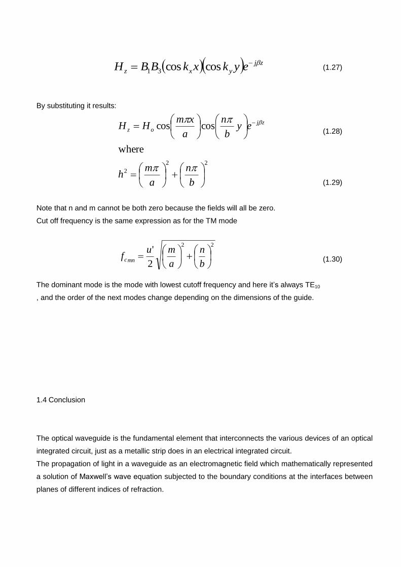
(1.27)
By substituting it results:
(1.28)
(1.29)
Note that n and m cannot be both zero because the fields will all be zero.
Cut off frequency is the same expression as for the TM mode
(1.30)
The dominant mode is the mode with lowest cutoff frequency and here it‘s always TE10
, and the order of the next modes change depending on the dimensions of the guide.
1.4 Conclusion
The optical waveguide is the fundamental element that interconnects the various devices of an optical
integrated circuit, just as a metallic strip does in an electrical integrated circuit.
The propagation of light in a waveguide as an electromagnetic field which mathematically represented
a solution of Maxwell‘s wave equation subjected to the boundary conditions at the interfaces between
planes of different indices of refraction.
zj
yxz eykxkBBH coscos31
22
2
where
coscos
b
n
a
mh
eyb
n
a
xmHH zj
oz
22
2
'
b
n
a
muf
mnc
Snell‘s law is important to represent the moving light behavior between two medias of different
refractive index n,and that leads to the total internal reflection which the light is totally confined in the
waveguide happens when the critical angle is greater or equal to .
The electromagnetic field pattern of radiation measured in a plane perpendicular to the propagation
direction of the beam is called a transverse mode which occurs because of boundary conditions
imposed on the wave by the waveguide.
A transverse magnetic (TM) mode happens when there‘s no magnetic fields in the direction of
propagation while the transverse electric (TE) modes: no electric field in the direction of propagation.
The cutoff frequency is the frequency below which attenuation occurs and above which propagation
takes place (High Pass).
Chapter 2
A Glimpse on the Silicon on Insulator
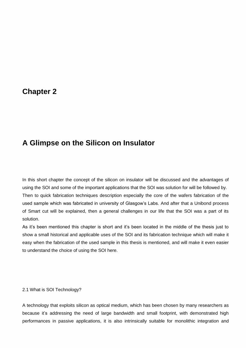
In this short chapter the concept of the silicon on insulator will be discussed and the advantages of
using the SOI and some of the important applications that the SOI was solution for will be followed by.
Then to quick fabrication techniques description especially the core of the wafers fabrication of the
used sample which was fabricated in university of Glasgow‘s Labs. And after that a Unibond process
of Smart cut will be explained, then a general challenges in our life that the SOI was a part of its
solution.
As it‘s been mentioned this chapter is short and it‘s been located in the middle of the thesis just to
show a small historical and applicable uses of the SOI and its fabrication technique which will make it
easy when the fabrication of the used sample in this thesis is mentioned, and will make it even easier
to understand the choice of using the SOI here.
2.1 What is SOI Technology?
A technology that exploits silicon as optical medium, which has been chosen by many researchers as
because it‘s addressing the need of large bandwidth and small footprint, with demonstrated high
performances in passive applications, it is also intrinsically suitable for monolithic integration and
compatible with microelectronics platform, discovering, moreover, interesting perspectives like non-
linear application and fast activation [89].
Also the transparency range of silicon extends from 1.1 μm to the far infrared region, covering
therefore both second and third windows of optical communications, and suggested, since the late
1980s, the exploitation of silicon for photonic applications [90].
SOI technology provides a very high refractive index n = 3.5 at λ = 1550 nm, so for device with silica
upper cladding, an index contrast Δn = 1.4. [91] Due to the high confinement of the optical
field, typical waveguide cross sections are 220×500 nm2 (Same core space of the sample used in this
thesis which been designed in Glasgow‘s University Laboratories).
The features of silicon photonics has become the choice for passive optical components [92], like
filters (which will be presented in chapter 4 by the Bragg grating), multiplexers / demultiplexers,
add/drop, interconnecting and routing networks, and so on.
Although an amount of features has been developed all over the past couple of decades yet the main
drawback of the high index contrast of silicon is the scattering process due to sidewall roughness, that
becoming the dominant contribution to losses, is the main issue to face for silicon photonic devices
development [93].
Since waveguides with sub-micrometers cross section are employed, few nanometers amplitude of
roughness is enough to produce significant values of propagation losses (for instance , it‘ll be shown
that for a widths 400 nm results a loss coefficient α ≈ 4 dB/cm).
Moreover, high confinement of the optical field makes the component more sensitive to fabrication
tolerances, because small inaccuracies cause non-negligible alteration of the propagating mode,
having a detrimental impact over the device performances.
Another drawback of SOI technology concerns the coupling between silicon chip and optical fibers. By
increasing light confinement, the waveguide mode field diameter consequently decreases which drop
down the efficiency. [91] (the coupling technique used in the thesis is end fire coupling, will be
explained later on section 3.4)
Another interesting feature of SOI technology is the possibility, exploiting directly polarized p-n
junctions, to modify the core refractive index by injecting free carriers [94]. This peculiarity, that
promises to realize a more efficient tuning of optical devices.
Several SOI advanced devices have been recently reported in literature, not only for passive
functions, like coupled resonator architectures [95], waveguide gratings [96] (the thesis subject of
interest) and routing matrices [97] and more challenging active tasks.
2.2 SOI Wafers Fabrication
2.2.1 The Fabrication Technique
The standard material for silicon photonics is the SOI wafer, produced by UNIBOND process
[99][100], that is composed by three layers. The top one is the silicon layer that is patterned in a
suitable way to become the guiding core of the optical circuits; typical nominal thickness of 220
nm enables single mode regime in the vertical direction. Below the core layer, a buried oxide (BOX)
SiO2 layer, grown by thermal oxidation, forms the lower cladding of the waveguides; a thick insulator
buffer (in this thesis work it‘s 2 μm) between guiding layer and substrate, allows to have negligible
leakage losses. Finally, the bottom layer, made of bulk silicon crystal, has a thickness of about 700 μm
and gives mechanical stability to the wafer.
The most common fabrication processes for SOI technology [101][102], employed for example by IBM
and NTT, exploit a silica intermediate masking layer in the pattern transfer from resist level to silicon
level, to avoid that employed relatively soft resists are degraded too quickly by a direct silicon etching
process, resulting in pattern edge damage and loss of small feature sizes.
As shown in Fig. 2.1 (a), four main fabrication steps are therefore generally required: silica
Deposition; resist coating, patterning (by electron-beam or photolithography) and development; silica
etching; silicon etching.
The developed process, shown in Fig. 3.3 (b) includes, instead, only two main steps: resist coating,
patterning (by electron-beam lithography) and development; silicon etching.
This reduction in the number of steps was achieved by the use of a highly dry-etch resistant resist that
made the use of a separate silica layer unnecessary.
This approach practically halved the process complexity and, since the intermediate silica mask is
considered to be the main source of roughness, resulted in better quality and reproducibility.
The resist employed is HSQ (Hydrogen SilsesQuioxane), a spin-on glass material that relatively
recently has been demonstrated as a negative tone resist (A positive resist undergoes chain-scission
and becomes soluble, while a negative resist reacts to electrons by cross-linking or becoming
insoluble) with very high resolution capability [103].
A 220 nm thick film is spinned on the top layer of the chip, baked, and patterned using a sequential
writing lithographic technique; the resist is then developed using TMAH (Tetra-Methyl-Ammonium
Hydroxide) at 25% concentration in water, to leave behind the exposed insoluble areas.
Although parallel photolithography is characterized by faster writing times, allowing mass production,
sequential writing lithographic technique, orders of magnitude slower, is however characterized by
higher degree of accuracy and programmability, allowing to produce fast turnaround in prototype
design and testing and to generate masks for optical lithography.[91]
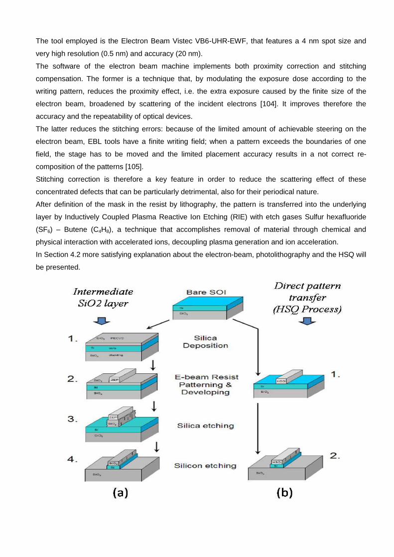
The tool employed is the Electron Beam Vistec VB6-UHR-EWF, that features a 4 nm spot size and
very high resolution (0.5 nm) and accuracy (20 nm).
The software of the electron beam machine implements both proximity correction and stitching
compensation. The former is a technique that, by modulating the exposure dose according to the
writing pattern, reduces the proximity effect, i.e. the extra exposure caused by the finite size of the
electron beam, broadened by scattering of the incident electrons [104]. It improves therefore the
accuracy and the repeatability of optical devices.
The latter reduces the stitching errors: because of the limited amount of achievable steering on the
electron beam, EBL tools have a finite writing field; when a pattern exceeds the boundaries of one
field, the stage has to be moved and the limited placement accuracy results in a not correct re-
composition of the patterns [105].
Stitching correction is therefore a key feature in order to reduce the scattering effect of these
concentrated defects that can be particularly detrimental, also for their periodical nature.
After definition of the mask in the resist by lithography, the pattern is transferred into the underlying
layer by Inductively Coupled Plasma Reactive Ion Etching (RIE) with etch gases Sulfur hexafluoride
(SF6) – Butene (C4H8), a technique that accomplishes removal of material through chemical and
physical interaction with accelerated ions, decoupling plasma generation and ion acceleration.
In Section 4.2 more satisfying explanation about the electron-beam, photolithography and the HSQ will
be presented.
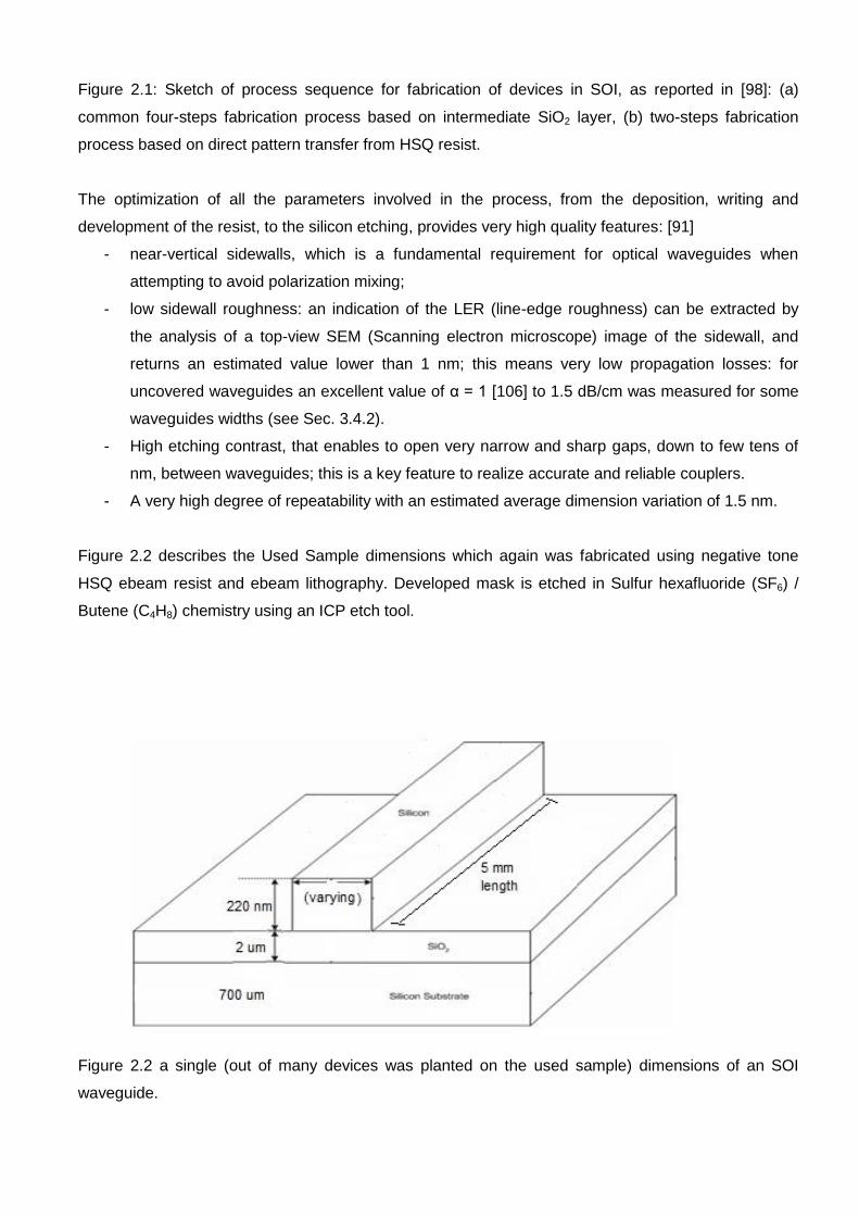
Figure 2.1: Sketch of process sequence for fabrication of devices in SOI, as reported in [98]: (a)
common four-steps fabrication process based on intermediate SiO2 layer, (b) two-steps fabrication
process based on direct pattern transfer from HSQ resist.
The optimization of all the parameters involved in the process, from the deposition, writing and
development of the resist, to the silicon etching, provides very high quality features: [91]
- near-vertical sidewalls, which is a fundamental requirement for optical waveguides when
attempting to avoid polarization mixing;
- low sidewall roughness: an indication of the LER (line-edge roughness) can be extracted by
the analysis of a top-view SEM (Scanning electron microscope) image of the sidewall, and
returns an estimated value lower than 1 nm; this means very low propagation losses: for
uncovered waveguides an excellent value of α = 1 [106] to 1.5 dB/cm was measured for some
waveguides widths (see Sec. 3.4.2).
- High etching contrast, that enables to open very narrow and sharp gaps, down to few tens of
nm, between waveguides; this is a key feature to realize accurate and reliable couplers.
- A very high degree of repeatability with an estimated average dimension variation of 1.5 nm.
Figure 2.2 describes the Used Sample dimensions which again was fabricated using negative tone
HSQ ebeam resist and ebeam lithography. Developed mask is etched in Sulfur hexafluoride (SF6) /
Butene (C4H8) chemistry using an ICP etch tool.
Figure 2.2 a single (out of many devices was planted on the used sample) dimensions of an SOI
waveguide.
2.2.2 Smart Cut
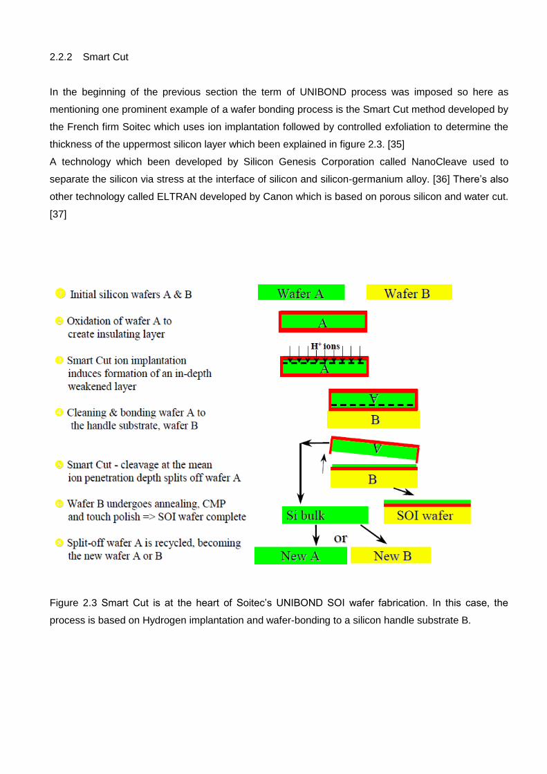
In the beginning of the previous section the term of UNIBOND process was imposed so here as
mentioning one prominent example of a wafer bonding process is the Smart Cut method developed by
the French firm Soitec which uses ion implantation followed by controlled exfoliation to determine the
thickness of the uppermost silicon layer which been explained in figure 2.3. [35]
A technology which been developed by Silicon Genesis Corporation called NanoCleave used to
separate the silicon via stress at the interface of silicon and silicon-germanium alloy. [36] There‘s also
other technology called ELTRAN developed by Canon which is based on porous silicon and water cut.
[37]
Figure 2.3 Smart Cut is at the heart of Soitec‘s UNIBOND SOI wafer fabrication. In this case, the
process is based on Hydrogen implantation and wafer-bonding to a silicon handle substrate B.

2.3 SOI Applications
SOI in general is taking over a huge part of our life whether in computing, Gaming, Automative,
Networking or even cameras and hand watches.
And it‘s been showed before that the SOI enables the best performance per watt, which means it
delivers more than 20% performance improvement and 35 to 40 power improvement, [40] here some
of the SOI applications will be presented by mentioning the challenges and the solution which been
found in the SOI.
1- Optical active cable
Challenge: In data centers connections between racks must be extremely fast to support
system speed.
Solution: SOI technology minimizes coupling and power dissipation. It allows integrating
multiple high-speed channels reliably in a small form factor. Also, SOI simplifies manufacturing
of wave-guides to interface CMOS circuits with optical fiber.
2- Optical waveguides
Challenge: To minimize signal loss and cost for optical interconnects both noise isolation and
precision manufacturing are essential for highly integrated solutions.
Solution: SOI Technology enables – for example – to combine on one die 25 silicon lasers
(with different frequencies) with 25 40 Gbps silicon modulators and multiplex them into one
output fiber.
3- CMOS image sensor
Challenge: Less expensive cameras and mobile phones demand small and low-cost image
sensors, without trading off sensitivity or quantum efficiency.
Solution: The oxide layer in the SOI wafers acts as an etch-stop and allows accurate and low-
cost manufacturing. Very uniform thinning of 300mm wafers, down to 5 um or less, is possible
and allows low-cost and high-quality CIS manufacturing.
4- Multi-GHz RF circuits
Challenge: In bulk-CMOS substrate currents reduce Q of inductors, especially in GHz range.
Solution: In SOI wafers the top silicon film can be of low resistivity, while the silicon substrate
can be very high resistivity material which significantly improving the quality of passive
components.
5- Highly integrated radio
Challenge: In bulk-CMOS it‘s difficult /costly to separate sensitive circuit elements sufficiently,
due to significant substrate- and cross-coupling.
Solution: The BOX in SOI wafers isolates the active circuitry from the HR-substrate and
minimizes these coupling effects. Also, the lateral oxide isolation between circuit elements
separates transistors better than junction isolation and consumers less area.

2.4 Conclusion
SOI is technology that exploits silicon as optical medium because of the need of large BW and the
small footprint as its compatibility with microelectronics platform the main drawback of the high index
contrast of silicon is the scattering process due to sidewall roughness.
The standard material for silicon photonics is the SOI wafer, produced by UNIBOND process such as
smart cut.
The four main fabrication steps are therefore generally required: silica Deposition; resist coating,
patterning (by electron-beam or photolithography) and development; silica etching; silicon etching.
There are many applications challenges in our life that the SOI was a good solution for.
Chapter 3
Waveguides Losses
In this chapter the types of the losses will be presented as for the definition of the Fabry-Perot method
and using it to calculate the propagation loss in the simple waveguides with different widths, and a first
look on the modal scattering in the waveguide with presenting the percentage of the scattered TM with
respect to the total TE and TM intensities will be illustrated in with some of the results that have been
measured.
3.1 Attenuation coefficient
The attenuation coefficient is a quantity that characterizes how easily a material or medium can be
penetrated by a beam of light, sound, particles, or other energy or matter. A large attenuation
coefficient means that the beam is quickly "attenuated" (weakened) as it passes through the medium,
and a small attenuation coefficient means that the medium is relatively transparent to the beam.
Attenuation coefficient is measured using units of reciprocal length. [77]
3.1.1 Definition and formula
The measured intensity of transmitted through a layer of material with thickness is related to the
incident intensity according to the inverse exponential power law that is usually referred to as Beer–
Lambert law:
(3.1)
Where denotes the path length. The attenuation coefficient (or linear attenuation coefficient) is .
3.2 Losses In Waveguides
One of the most important characteristic of a waveguide is the attenuation, or loss, that a light wave
experiences as it travels through the guide. This loss is generally attributable to three different
mechanisms: Scattering, absorption and radiation. Scattering loss usually predominates in glass or
dielectric waveguides, while absorption loss is most important in semiconductors and other crystalline
materials. Radiation losses become significant when waveguides are bent through a curve. [1]
3.2.1 Scattering Losses
Scattering loss occurs when electromagnetic waves interact with scattering centers of a size smaller
than the wavelength. Because of the small size of the scattering centers, which can be due to impurity
clusters and localized dielectric fluctuations, they can be viewed as uniformly excited by the field.[2]
In an ideal waveguide the modes are orthogonal, so that no energy will be coupled from the lower-
order modes to the higher-order modes. However, waveguide irregularities and inhomogeneities can
cause mode conversion, so that energy is coupled from lower-order to higher-order modes. [11]
There are two types of scattering loss in an optical waveguide: volume (Rayleigh) scattering and
surface scattering. Volume scattering is caused by imperfections, and it follows either λ-3 dependence,
or λ-1 dependence, as a consequence of the type and concentration of scattering centers.
In Rayleigh scattering, each ―particle‖ is uniformly excited by the field and becomes polarized with a
dipole moment. So the absorption coefficient can be given by an equation referred to αR in [7].
The second type is surface scattering that results from surface roughness.
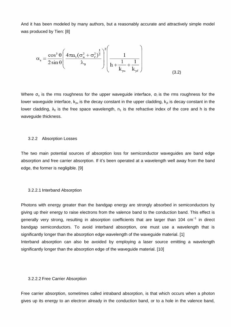
And it has been modeled by many authors, but a reasonably accurate and attractively simple model
was produced by Tien: [8]
(3.2)
Where σu is the rms roughness for the upper waveguide interface, σl is the rms roughness for the
lower waveguide interface, kyu is the decay constant in the upper cladding, kyl is decay constant in the
lower cladding, λ0 is the free space wavelength, n1 is the refractive index of the core and h is the
waveguide thickness.
3.2.2 Absorption Losses
The two main potential sources of absorption loss for semiconductor waveguides are band edge
absorption and free carrier absorption. If it‘s been operated at a wavelength well away from the band
edge, the former is negligible. [9]
3.2.2.1 Interband Absorption
Photons with energy greater than the bandgap energy are strongly absorbed in semiconductors by
giving up their energy to raise electrons from the valence band to the conduction band. This effect is
generally very strong, resulting in absorption coefficients that are larger than 104 cm−1 in direct
bandgap semiconductors. To avoid interband absorption, one must use a wavelength that is
significantly longer than the absorption edge wavelength of the waveguide material. [1]
Interband absorption can also be avoided by employing a laser source emitting a wavelength
significantly longer than the absorption edge of the waveguide material. [10]
3.2.2.2 Free Carrier Absorption
Free carrier absorption, sometimes called intraband absorption, is that which occurs when a photon
gives up its energy to an electron already in the conduction band, or to a hole in the valence band,
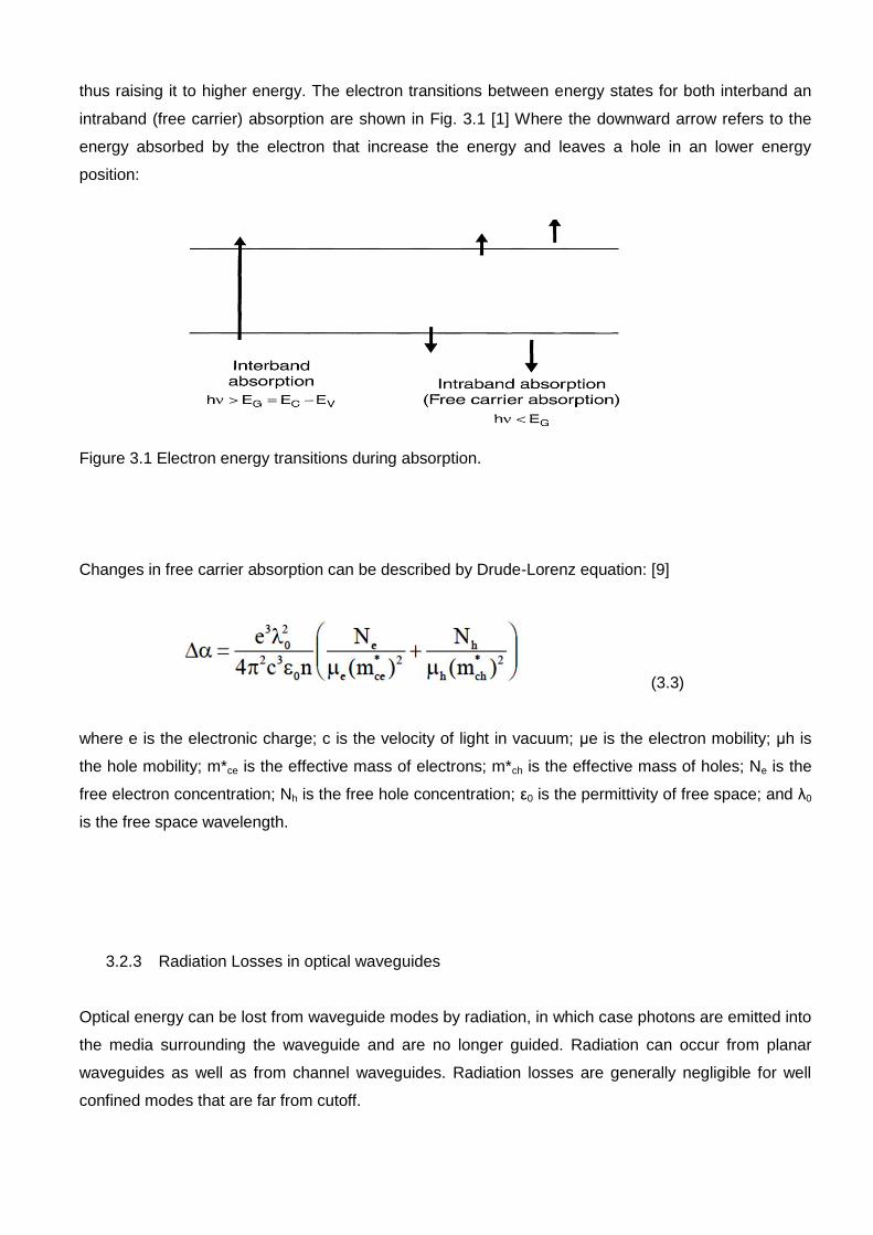
thus raising it to higher energy. The electron transitions between energy states for both interband an
intraband (free carrier) absorption are shown in Fig. 3.1 [1] Where the downward arrow refers to the
energy absorbed by the electron that increase the energy and leaves a hole in an lower energy
position:
Figure 3.1 Electron energy transitions during absorption.
Changes in free carrier absorption can be described by Drude-Lorenz equation: [9]
(3.3)
where e is the electronic charge; c is the velocity of light in vacuum; μe is the electron mobility; μh is
the hole mobility; m*ce is the effective mass of electrons; m*ch is the effective mass of holes; Ne is the
free electron concentration; Nh is the free hole concentration; ε0 is the permittivity of free space; and λ0
is the free space wavelength.
3.2.3 Radiation Losses in optical waveguides
Optical energy can be lost from waveguide modes by radiation, in which case photons are emitted into
the media surrounding the waveguide and are no longer guided. Radiation can occur from planar
waveguides as well as from channel waveguides. Radiation losses are generally negligible for well
confined modes that are far from cutoff.
However, at cutoff, all of the energy is transferred to the substrate radiation modes, Since the higher-
order modes of a waveguide are always either beyond cutoff or are at least, closer to cutoff than the
lower-order modes, radiation loss is greater for higher-order modes. [11] Though the precedent
knowledge of the waveguide width shall be a key factor to bring out the property of monomodal or
almost monomodal.
There Radiation Loss occurs by Curved Channel Waveguides Because of distortions of the optical
field that occurs when guided waves travel through a bend in a channel waveguide, radiation loss can
be greatly increased. In fact, the minimum allowable radius of curvature of a waveguide is generally
limited by radiation losses rather than by fabrication tolerances. [12]
3.3 Measurement of propagation loss in optical waveguides
There is confusion between insertion loss and propagation loss. The insertion loss of a device, is the
total loss associated with introducing that element into a system, and includes the inherent loss and
the coupling losses.
Inherent loss refers to the light loss in a waveguide that cannot be eliminated during the fabrication
process is due to impurities and roughness. [78] As for the coupling losses refers to the power loss
that occurs when coupling light from one optical device or medium to another, [79] which in the thesis
work shall be refer to coupling light from air to the waveguide yet it also will be taken care of as the
mode is well confined into the waveguide.
Alternatively, the propagation loss is the loss associated with propagation in the waveguide alone.
There are three main experimental techniques associated with waveguide measurement. These are (i)
the cut–back method; (ii) the Fabry-Perot resonance method; and (iii) scattered light measurement.
The cut back method is conceptually simple. A waveguide of length L is excited by one of the coupling
methods with an optical fiber like the grating couplers [80], inverse tapers [81] or tapered waveguides
[82], and in any of those the output power from the waveguide, and the input power to the waveguide
are recorded.
Waveguides have definite dimensions they are tapered to roughly 22 micron to couple light with the
fiber then fabrication of shorter and shorter waveguide sections and consequently longer and longer
taper sections with for instance another length, and the measurement repeated to determine the
output. Hence: [13]
(3.4)

i.e.
(3.5)
The scattered light measurements takes a place when the scattered light will be quantitatively
evaluated, however, the measurement requires assumptions to be made like the evaluation of the
angle-resolved scattered light measurement and the conversion into the surface parameter which
makes the process not really easy.
3.3.1 Using Fabry-Perot Resonance Method
The used chip facet is reflective which make it form a cavity. This cavity has an input and an output
mirrors, and noticing this structure makes the Fabry Perot cavity method presented.
The Fabry-Perot etalon, or interferometer, named after its inventors [15] designed in 1899. Fabry and
A. Perot, represents a significant improvement over the Michelson [114] interferometer. The
difference between the two lies in the fact that the Fabry-Perot design contains plane surfaces that are
all partially reflecting so that multiple rays of light are responsible for creation of the observed
interference patterns.
Fabry-Perot optical resonator is a resonant cavity formed by two parallel reflecting mirrors separated
by a medium.
When the mirrors are aligned perfectly parallel to each other, the reflections of the light waves
between the two mirrors interfere constructively and destructively, giving rise to a standing wave
pattern between the mirror surfaces, just like standing waves on a string, see Figure 1.4. For standing
waves, any wavelengths that are not an integer multiple of half a wavelength will interfere
destructively.
The ratio of the mode separation to the spectral width is called the finesse (F) of the cavity and is
given by: [16]
(3.6)
Where FSR is the free spectral range which is the difference in frequency between consecutive
interference fringes and Δf is the minimum resolvable bandwidth or resolution which is the width (full
width at half maximum peak intensity) of an interference fringe generated when a perfectly
monochromatic light source is transmitted by a Fabry-Perot. [17]
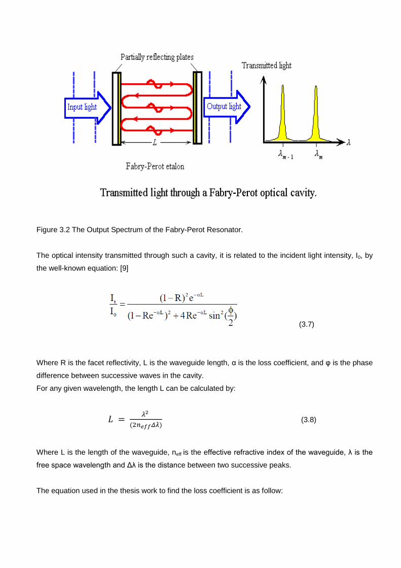
Figure 3.2 The Output Spectrum of the Fabry-Perot Resonator.
The optical intensity transmitted through such a cavity, it is related to the incident light intensity, I0, by
the well-known equation: [9]
(3.7)
Where R is the facet reflectivity, L is the waveguide length, α is the loss coefficient, and φ is the phase
difference between successive waves in the cavity.
For any given wavelength, the length L can be calculated by:
(3.8)
Where L is the length of the waveguide, neff is the effective refractive index of the waveguide, λ is the
free space wavelength and Δλ is the distance between two successive peaks.
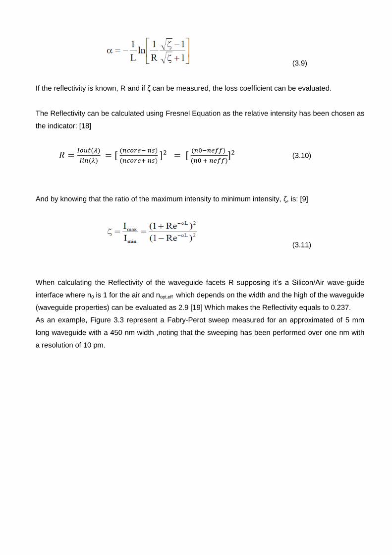
The equation used in the thesis work to find the loss coefficient is as follow:
(3.9)
If the reflectivity is known, R and if ζ can be measured, the loss coefficient can be evaluated.
The Reflectivity can be calculated using Fresnel Equation as the relative intensity has been chosen as
the indicator: [18]
(3.10)
And by knowing that the ratio of the maximum intensity to minimum intensity, ζ, is: [9]
(3.11)
When calculating the Reflectivity of the waveguide facets R supposing it‘s a Silicon/Air wave-guide
interface where n0 is 1 for the air and nopt,eff which depends on the width and the high of the waveguide
(waveguide properties) can be evaluated as 2.9 [19] Which makes the Reflectivity equals to 0.237.
As an example, Figure 3.3 represent a Fabry-Perot sweep measured for an approximated of 5 mm
long waveguide with a 450 nm width ,noting that the sweeping has been performed over one nm with
a resolution of 10 pm.

Figure 3.3 Example on Fabry-Perot scanning.
As the figure above shows the distance between a random two successive peaks and the maximum
and minimum intensity which will be helpful to determine the loss.
So for instance in the previous Figure (3.3) on a specific fringe when getting Imax = 64.52 and Imin =
38.44, finding an amount of the loss coefficient α using equation 1.20 equals to -1.22 and a Loss
(dB/cm) (regarding to the upcoming formula 3.13) equals to 5.29 dB/cm at that wavelength.
Though, here a nearly same but high precision simple expression to fabry-perot method to get more
accurate loss measurements will be employed given by: [20]
(3.12)
Where the visibility of the fringes, R is is the end-face (power)
reflectivity, and L is the waveguide length.
For even more fair and precise calculations the average of the fringes intensity will be used, meaning
that Imax will be referring to the average value of all the maximum fringes (Imax,Avg) and same as for the
Imin .

Noting that the loss coefficient α will be represented by (cm-1), and the loss is usually represented by
(dB/cm) and to get that the formula below is used:
(3.13)
3.4 Experimental Set-Up
In the first three sections of this chapter quick review was presented to the concept of waveguides
losses, though here in this section a closer look on the set up that has been used to measure the loss
in the waveguide using the simple extension of the Fabry-Perot technique will be illustrated and a
better look and understanding on the polarization effect on measuring the loss shall be shown.
First, to have a better look on what it‘s been dealt with on the Laboratory the concept of End-Fire
Coupling to Waveguides has to be mentioned which is one of the simplest, and also most accurate,
methods of measuring waveguide loss is to focus light of the desired wavelength directly onto a
polished or cleaved input face of a waveguide as shown in Figure 3.4
Figure 3.4 Experimental set-up for measurement of waveguide attenuation employing end-fire
coupling.
This method will be a general concept will be put in mind because it‘s going to be helpful to use it on a
several amount of waveguides that varies whether by length or width.
Often this series of measurements is performed by beginning with a relatively long waveguide sample,
then repetitively shortening. [21]
Care must be taken before each measurement to align the laser beam and the sample for optimum
coupling, by maximizing the observed output power. The extent of the scatter of the data points is a
measure of the consistency of sample input/output coupling loss, which depends on face preparation,
and on sample alignment.
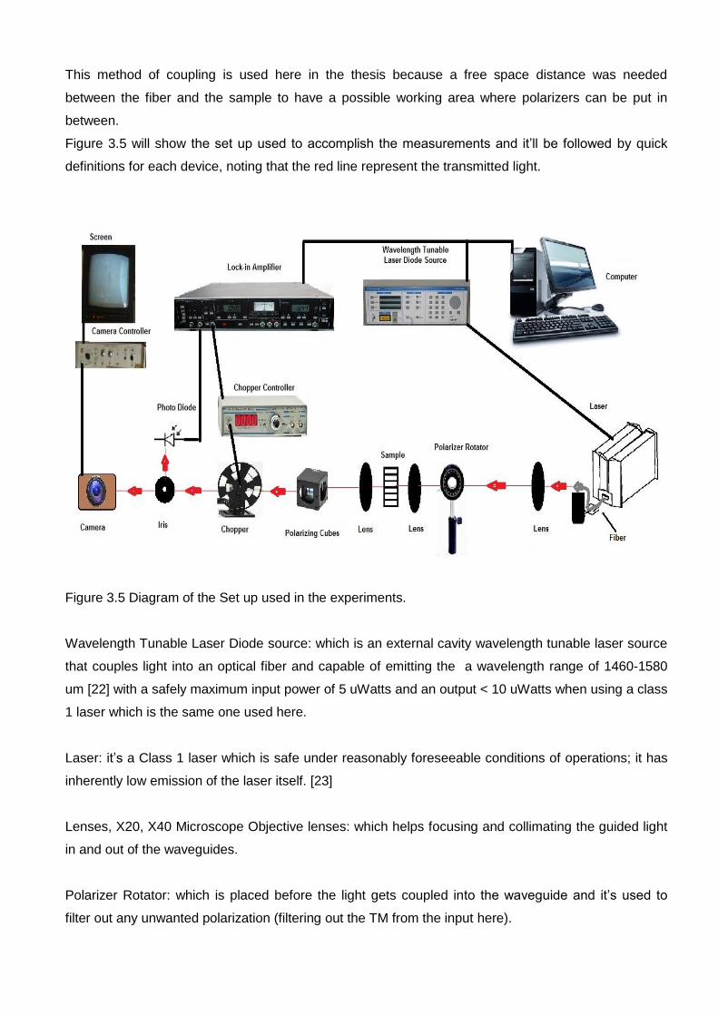
This method of coupling is used here in the thesis because a free space distance was needed
between the fiber and the sample to have a possible working area where polarizers can be put in
between.
Figure 3.5 will show the set up used to accomplish the measurements and it‘ll be followed by quick
definitions for each device, noting that the red line represent the transmitted light.
Figure 3.5 Diagram of the Set up used in the experiments.
Wavelength Tunable Laser Diode source: which is an external cavity wavelength tunable laser source
that couples light into an optical fiber and capable of emitting the a wavelength range of 1460-1580
um [22] with a safely maximum input power of 5 uWatts and an output < 10 uWatts when using a class
1 laser which is the same one used here.
Laser: it‘s a Class 1 laser which is safe under reasonably foreseeable conditions of operations; it has
inherently low emission of the laser itself. [23]
Lenses, X20, X40 Microscope Objective lenses: which helps focusing and collimating the guided light
in and out of the waveguides.
Polarizer Rotator: which is placed before the light gets coupled into the waveguide and it‘s used to
filter out any unwanted polarization (filtering out the TM from the input here).
The Sample: it‘s worth to mention that the Sample shall be placed on the Micro Positioner which is
used to set a precise alignment.
Polarizing Cube: placed after the lese on the output and it again filter out the unwanted polarization
but from the output this time, noting that in this part of the thesis both cases of the output TE and TM
will be experimented.
Chopper: which used to modulate the output light and it‘s been set to a frequency using its controller.
Iris: which controls the amount of light that passes through to the Photo Diode ,trying to make sure
that only the light coming out of the waveguide is the one has been detect.
Photo Diode: Detecting the output light, it‘s connected to lock-in Amplifier.
Lock-in Amplifier: it‘s an instrument with dual capability that can recover signals in the presence of
overwhelming noise background or alternatively it can provide high resolution measurements of
relatively clean signals over several orders of magnitude and frequency. [24]
Computer: which connected to the Wavelength Tunable Laser Diode source and the Lock-in Amplifier
using a GPIB (general purpose interface bus) , and simply using a Lab View software
(TUNICS_TODDV2.3) The wavelength Span set, launch the Laser and get the results of the sweeping
graphically on the screen and saved as a text file.
3.4.1 Used Device Characterization
The Sample was fabricated using negative tone HSQ e-beam resist and e-beam lithography and the
Developed mask is etched in SF6/C4H8 chemistry using an ICP etch tool.
The sample used in this thesis is designed as followed (shown previously in Figure 2.1):
- 220 nm thick core layer
- 2 um SiO2 under-cladding layer
- The waveguides have variable widths.
- 5 mm length to have three sets of devices interspersed by slabs.
Set 1 is Pi-shifted Bragg gratings and which will be discussed in chapter 4, Set 2 which is the set that
would be the center of concerns in this chapter and there are a simple waveguides 5 replicas of each
device.
Top to bottom the widths laterally varies as 1000,900,800,700,600,550,500,450,400 nm and last set is
a rings and it won‘t be mentioned in this thesis.
3.4.2 Results and Discussion
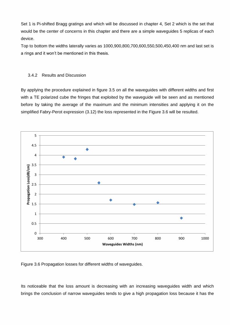
By applying the procedure explained in figure 3.5 on all the waveguides with different widths and first
with a TE polarized cube the fringes that exploited by the waveguide will be seen and as mentioned
before by taking the average of the maximum and the minimum intensities and applying it on the
simplified Fabry-Perot expression (3.12) the loss represented in the Figure 3.6 will be resulted.
Figure 3.6 Propagation losses for different widths of waveguides.
Its noticeable that the loss amount is decreasing with an increasing waveguides width and which
brings the conclusion of narrow waveguides tends to give a high propagation loss because it has the
0
0.5
1
1.5
2
2.5
3
3.5
4
4.5
5
300 400 500 600 700 800 900 1000
Pro
pag
atio
n L
oss
(dB
/cm
)
Waveguides Widths (nm)
behavior of confining the light in the center of the waveguide and that all happen as a result of the
strong interaction of the mode with the sidewalls which lead to a large scattering inside the waveguide.
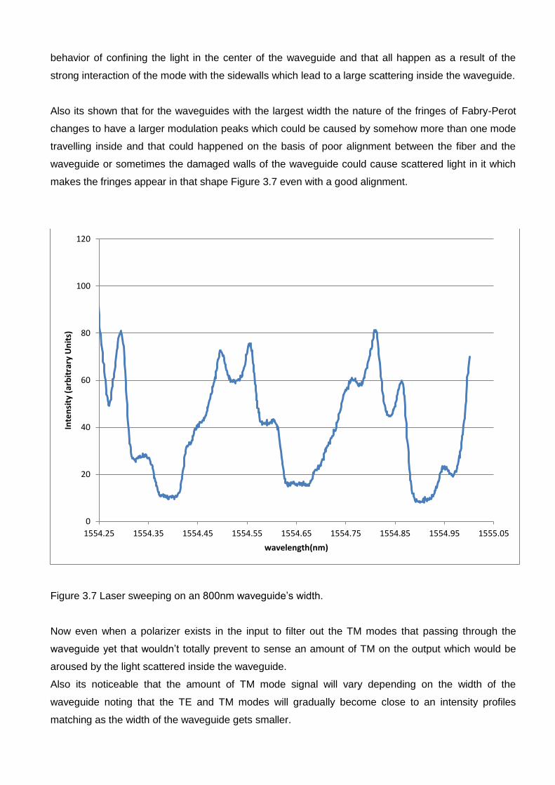
Also its shown that for the waveguides with the largest width the nature of the fringes of Fabry-Perot
changes to have a larger modulation peaks which could be caused by somehow more than one mode
travelling inside and that could happened on the basis of poor alignment between the fiber and the
waveguide or sometimes the damaged walls of the waveguide could cause scattered light in it which
makes the fringes appear in that shape Figure 3.7 even with a good alignment.
Figure 3.7 Laser sweeping on an 800nm waveguide‘s width.
Now even when a polarizer exists in the input to filter out the TM modes that passing through the
waveguide yet that wouldn‘t totally prevent to sense an amount of TM on the output which would be
aroused by the light scattered inside the waveguide.
Also its noticeable that the amount of TM mode signal will vary depending on the width of the
waveguide noting that the TE and TM modes will gradually become close to an intensity profiles
matching as the width of the waveguide gets smaller.
0
20
40
60
80
100
120
1554.25 1554.35 1554.45 1554.55 1554.65 1554.75 1554.85 1554.95 1555.05
Inte
nsi
ty (
arb
itra
ry U
nit
s)
wavelength(nm)
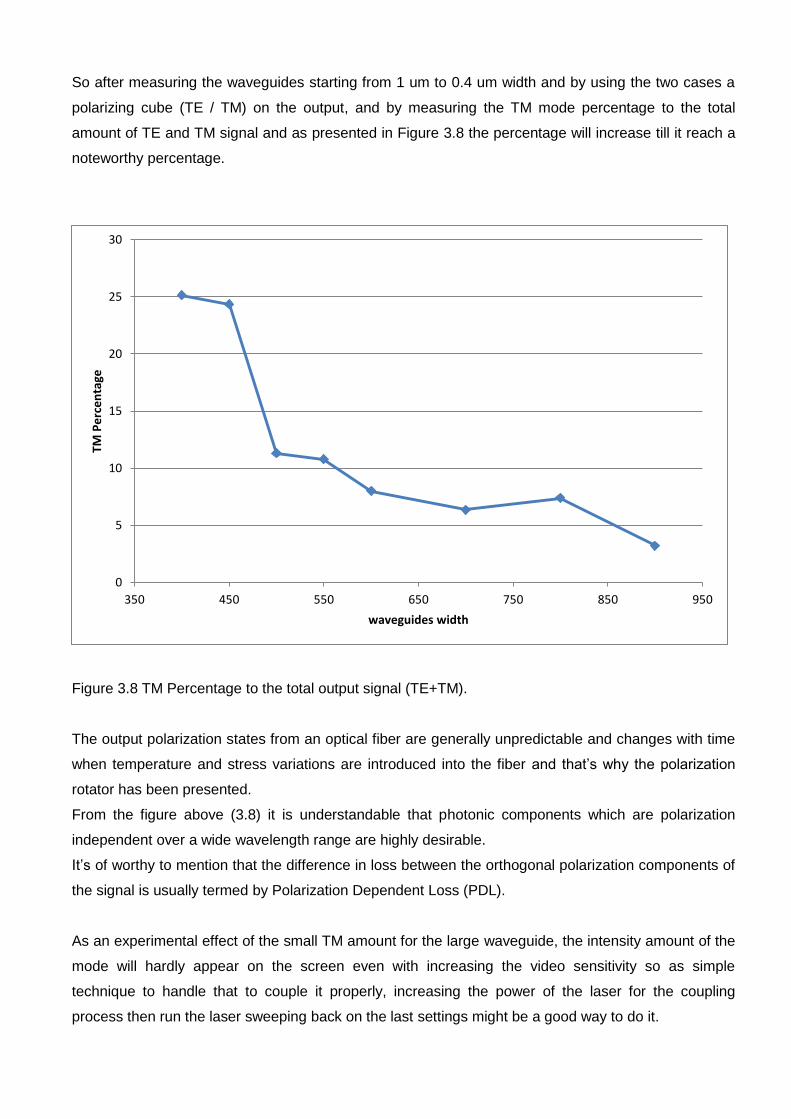
So after measuring the waveguides starting from 1 um to 0.4 um width and by using the two cases a
polarizing cube (TE / TM) on the output, and by measuring the TM mode percentage to the total
amount of TE and TM signal and as presented in Figure 3.8 the percentage will increase till it reach a
noteworthy percentage.
Figure 3.8 TM Percentage to the total output signal (TE+TM).
The output polarization states from an optical fiber are generally unpredictable and changes with time
when temperature and stress variations are introduced into the fiber and that‘s why the polarization
rotator has been presented.
From the figure above (3.8) it is understandable that photonic components which are polarization
independent over a wide wavelength range are highly desirable.
It‘s of worthy to mention that the difference in loss between the orthogonal polarization components of
the signal is usually termed by Polarization Dependent Loss (PDL).
As an experimental effect of the small TM amount for the large waveguide, the intensity amount of the
mode will hardly appear on the screen even with increasing the video sensitivity so as simple
technique to handle that to couple it properly, increasing the power of the laser for the coupling
process then run the laser sweeping back on the last settings might be a good way to do it.
0
5
10
15
20
25
30
350 450 550 650 750 850 950
TM P
erc
en
tage
waveguides width

3.5 Conclusion
Using Fabry-Perot method to calculate the loss coefficient is effective because the chip facet is
reflective which make a cavity, and it depends on the reflectivity, waveguide length and the intensities
(output, input).
Care must be taken before each measurement to align the laser beam and the sample for optimum
coupling, by maximizing the observed output power.
The propagation loss amount decreases as the wavelength width increase and that‘s because of the
behavior of confining the light in the center of the waveguide and that all happen as a result of the
strong interaction of the mode with the sidewalls.
The TM mode gradually increases as the waveguides widths get smaller which also refers to the
amount of scattered light in that waveguide.
Chapter 4
Bragg Grating
In this last chapter which would be the backbone of the thesis title and the core of what have been
presented in the previous chapters. Introduction to the Bragg Grating and how it works. Then some of
the Integrated Bragg Grating fabrication techniques will be presented and accordingly a description of
the fabrication method used on the sample used in this thesis work will be mentioned and explained
extensively as an extension of the fabrication process that has been shown in chapter 2 and the final
section a better understanding on the characterization of the Bragg Grating in a general way and on
more specified one considering the polarization effect is expected.
4.1 What‘s Bragg Grating
A Bragg grating is a periodic perturbation of the refractive index along a specific length which is
formed by exposure of the core to an intense optical interference pattern. [41]
The formation of permanent gratings was first introduced in the optical fiber and was first
demonstrated by Hill et al. in 1978 at the Canadian Communications Research Centre (CRC), Ottawa,
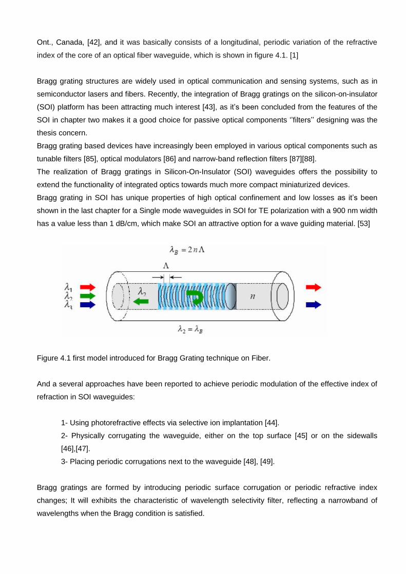
Ont., Canada, [42], and it was basically consists of a longitudinal, periodic variation of the refractive
index of the core of an optical fiber waveguide, which is shown in figure 4.1. [1]
Bragg grating structures are widely used in optical communication and sensing systems, such as in
semiconductor lasers and fibers. Recently, the integration of Bragg gratings on the silicon-on-insulator
(SOI) platform has been attracting much interest [43], as it‘s been concluded from the features of the
SOI in chapter two makes it a good choice for passive optical components ‗‘filters‘‘ designing was the
thesis concern.
Bragg grating based devices have increasingly been employed in various optical components such as
tunable filters [85], optical modulators [86] and narrow-band reflection filters [87][88].
The realization of Bragg gratings in Silicon-On-Insulator (SOI) waveguides offers the possibility to
extend the functionality of integrated optics towards much more compact miniaturized devices.
Bragg grating in SOI has unique properties of high optical confinement and low losses as it‘s been
shown in the last chapter for a Single mode waveguides in SOI for TE polarization with a 900 nm width
has a value less than 1 dB/cm, which make SOI an attractive option for a wave guiding material. [53]
Figure 4.1 first model introduced for Bragg Grating technique on Fiber.
And a several approaches have been reported to achieve periodic modulation of the effective index of
refraction in SOI waveguides:
1- Using photorefractive effects via selective ion implantation [44].
2- Physically corrugating the waveguide, either on the top surface [45] or on the sidewalls
[46],[47].
3- Placing periodic corrugations next to the waveguide [48], [49].
Bragg gratings are formed by introducing periodic surface corrugation or periodic refractive index
changes; It will exhibits the characteristic of wavelength selectivity filter, reflecting a narrowband of
wavelengths when the Bragg condition is satisfied.
(4.1)
Where λB is the Bragg wavelength, Λ is the period of the grating, neff is the effective index of the
structure and m is the grating order.
Based on equation (4.1) the spectral responses of the Bragg gratings can be customized with
refractive index modulation via precise etch depth, the period and the order of grating.
Various Bragg gratings on SOI waveguide have been reported though the majority of the grating is
utilizing 1st order gratings in large cross sectional area waveguides.
Which gives when m = 1:
(4.2)
Knowing that Bragg gratings are formed by introducing periodic surface corrugation or periodic
refractive index changes it will exhibits the characteristic of wavelength selectivity filter, reflecting a
narrowband of wavelengths when the Bragg condition is satisfied.
Generally the loss introduced by the gratings is negligible, as the corrugation width is increased, the
average effective index of refraction neff decreases [53]. Hence, shifting the reflectivity peak to shorter
wavelength by the Bragg condition Equation (4.1).
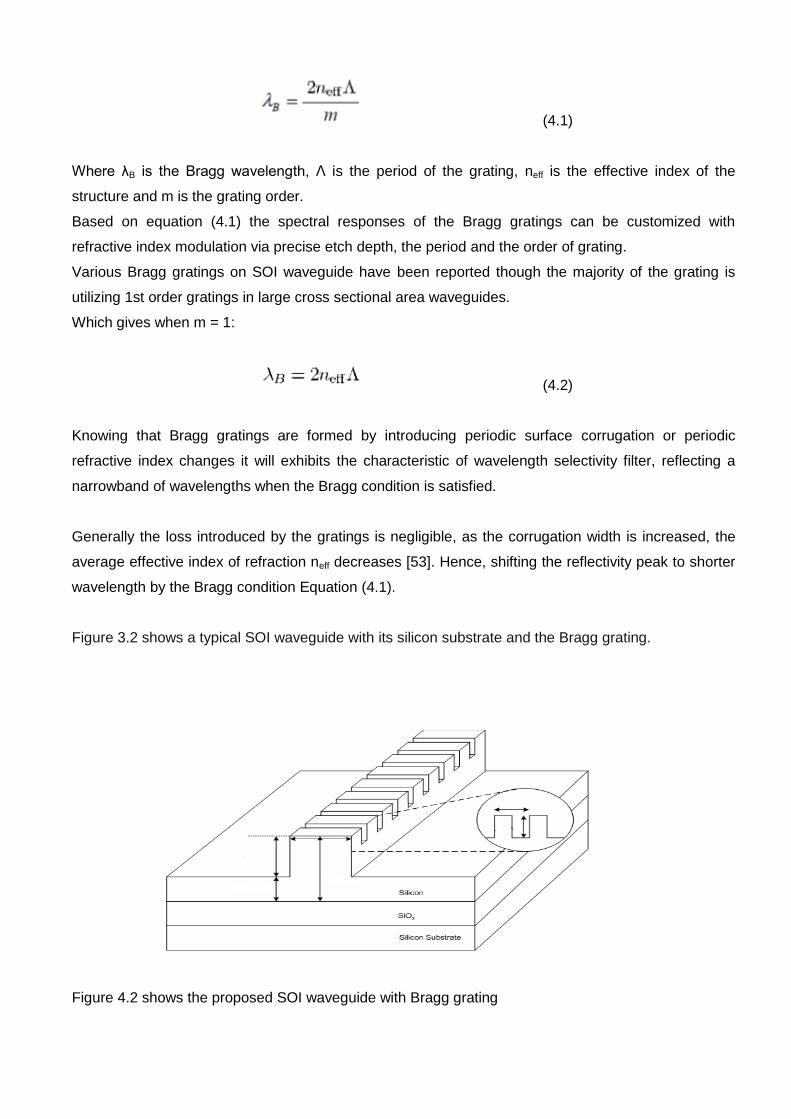
Figure 3.2 shows a typical SOI waveguide with its silicon substrate and the Bragg grating.
Figure 4.2 shows the proposed SOI waveguide with Bragg grating
4.2 Integrated Bragg Grating Fabrication Techniques
The fabrication method, First the grating pattern was exposed using E-beam lithography and
subsequently transferred into the semiconductor material via RIE processes.
4.2.1 Lithography
In the manufacture of integrated optoelectronic devices there are two main lithography techniques
that are widely employed; namely photolithography and Electron Beam lithography.
The decision on which method to use is based on a number of considerations such as the feature
size to be defined, the number of samples to be produced, the required flexibility in the design
stage, the size of the area to be written, the exposure time and the cost of production. Both
methods, if the process requires pattern transfer into a hard mask, will use similar Reactive Ion
Etching steps after the transfer of the mask pattern into the resist or soft
mask. The main distinction then is the method of transferring the mask into the resist.[108]
4.2.1.1 Photolithography
Photolithography uses a pre-patterned mask plate that carries the desired features to be
transferred onto the semiconductor. The sample is spun with photosensitive resist and baked to
evaporate the solvents.
There are a number of different methods of transferring the mask details into the resist depending
on the specific application; however, the main mechanism is the same. A light source is shone
through the mask, and any other processing optics required, and exposes areas of resist.
The resist exposed to the light is molecularly altered so that on development the developer
solution will only react with either the exposed or unexposed areas. The developer solution clears
the unwanted resist leaving only the information from the mask plate transferred into the
photoresist. Subsequently the sample can be processed using reactive ion etching depending on
the application. [108]
Photolithography is the technology of choice for large scale production as many features or
devices may be written simultaneously using a single mask. An entire wafer can be manufactured
in a single run with the exposure time limited only by the reaction of the photoresist.
However, the resolution of the photolithography is limited by the diffraction limit of the illumination.
Currently UV and deep UV sources are common in photolithography processes and can achieve
feature sizes of under a micron [107][109].
There are a number of limiting factors to the photolithographic techniques however. The speed of
the system is partially due to the single mask that is used in the processing cycle. The drawback of
using a mask is that if any modification is required in the pattern an entirely new mask must be
fabricated, meaning that while ideally suited to large scale, consistent
fabrication, photolithography is less appropriate for research work involving many different mask
designs. Also, as stated, the feature size of the pattern is limited to close to a micron whereas
many optical structures require features with dimensions significantly smaller than this limit. [108]
4.2.1.2 Electron-beam lithography
An alternative to photolithography is Electron Beam lithography. Rather than using a mask to
define the exposed areas of resist the E-beam writes onto the surface directly exposing the
required areas. Clearly this is a much slower process than the photolithography since the pattern is
serially written.
There are some significant benefits to be garnered from this technique however. Firstly, the pattern
is easily created and modified using CAD packages which quickly produce new designs that can
be implemented in short time scales allowing feedback of results into fabrication processes.
Current E-beam technology provides the opportunity to create feature sizes into the nanometre
range [110]. With this ease of modification and flexible nanometre scale device definition E-beam
lithography is an attractive option for the production of sub-micron scale optical structures in both
commercial and research environments and the choice in this thesis work.
4.2.2 E-beam resists and reactive ion etching
The final objective of creating three dimensional structures in semiconductor materials can be
viewed from two different perspectives. Firstly, the two dimensional pattern to be created must be
applied to the surface of the material; this is dealt with by the lithographic techniques discussed
previously.
Secondly, a method must be sought by which selective removal of the semiconductor material will
create a depth profile in the material. Clearly it is necessary to use the lithography to create a two
dimensional pattern that is then etched into the semiconductor
material. From the different perspectives described it is clear that the constraints on the method
require a layer that is receptive to lithography and a subsequent process that will selectively etch
the material under the pattern. [108]
There are a number of common resists used in conjunction with E-beam lithography, but it is
poly(methyl methacrylate), PMMA, that will be considered as an example here. The PMMA resist
is spun onto the sample, exposed with the E-beam system and subsequently developed with
MIBK:IPA solution to produce the pattern.
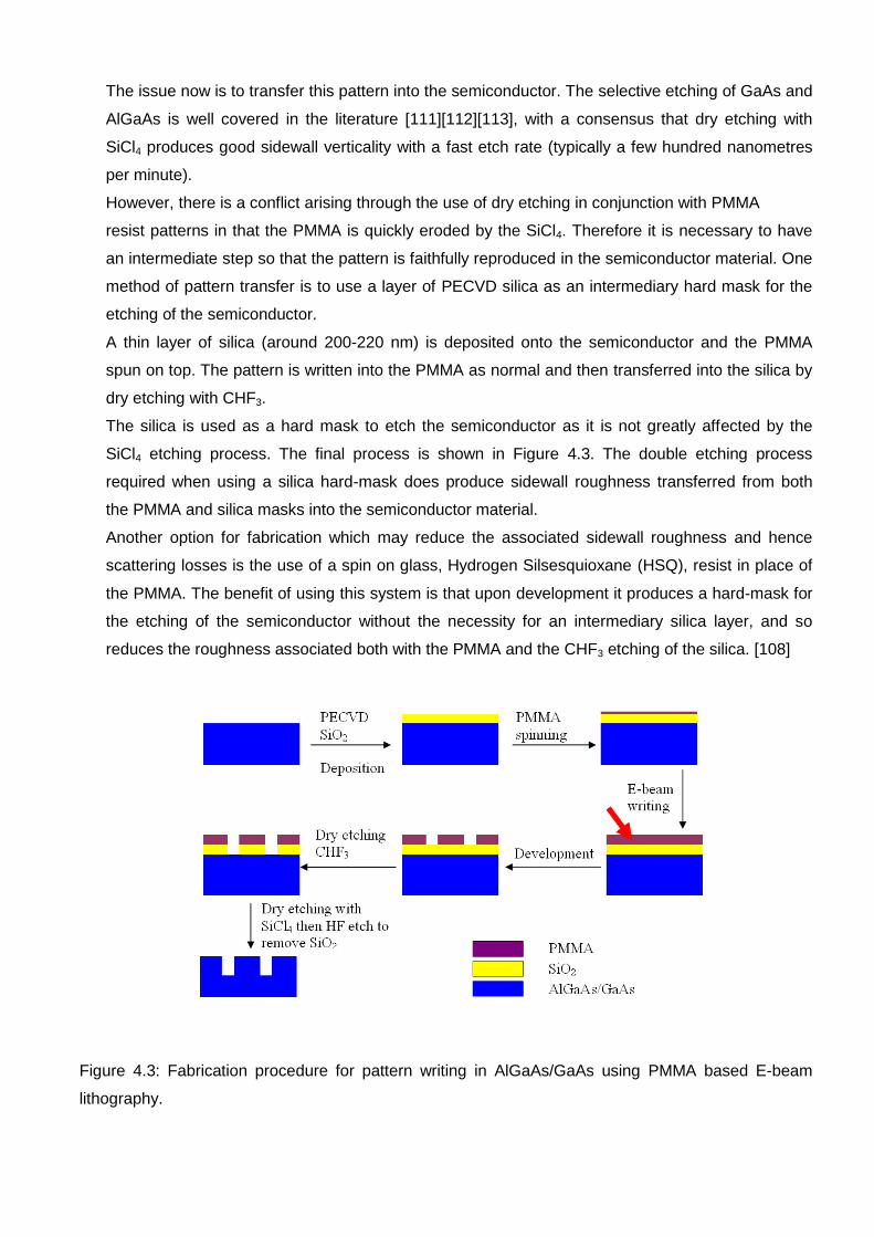
The issue now is to transfer this pattern into the semiconductor. The selective etching of GaAs and
AlGaAs is well covered in the literature [111][112][113], with a consensus that dry etching with
SiCl4 produces good sidewall verticality with a fast etch rate (typically a few hundred nanometres
per minute).
However, there is a conflict arising through the use of dry etching in conjunction with PMMA
resist patterns in that the PMMA is quickly eroded by the SiCl4. Therefore it is necessary to have
an intermediate step so that the pattern is faithfully reproduced in the semiconductor material. One
method of pattern transfer is to use a layer of PECVD silica as an intermediary hard mask for the
etching of the semiconductor.
A thin layer of silica (around 200-220 nm) is deposited onto the semiconductor and the PMMA
spun on top. The pattern is written into the PMMA as normal and then transferred into the silica by
dry etching with CHF3.
The silica is used as a hard mask to etch the semiconductor as it is not greatly affected by the
SiCl4 etching process. The final process is shown in Figure 4.3. The double etching process
required when using a silica hard-mask does produce sidewall roughness transferred from both
the PMMA and silica masks into the semiconductor material.
Another option for fabrication which may reduce the associated sidewall roughness and hence
scattering losses is the use of a spin on glass, Hydrogen Silsesquioxane (HSQ), resist in place of
the PMMA. The benefit of using this system is that upon development it produces a hard-mask for
the etching of the semiconductor without the necessity for an intermediary silica layer, and so
reduces the roughness associated both with the PMMA and the CHF3 etching of the silica. [108]
Figure 4.3: Fabrication procedure for pattern writing in AlGaAs/GaAs using PMMA based E-beam
lithography.
PMMA is a positive photoresist - meaning that exposed areas will be removed from the mask on
development. This being the case it is useful for opening contact windows, contact pad areas or
marker patterns, as in these cases it is only small portions of the sample that need to be opened to the
RIE or metal deposition processes.
However, if it is used to define waveguides a narrow unexposed area must be left between adjacent
exposed areas so that trenches are opened on either side of the waveguide on etching.
Though, since PMMA is a positive resist, writing these two large exposed areas so close to one
another causes problems with exposure of the waveguide pattern itself. When exposing resist with E-
beam lithography the substrate backscatters electrons into the resist, the radius of which exposure is
related to the exciting beam voltage and substrate material.
One effect of this process is the exposure of areas surrounding the focused spot due to the
backscattering. If a large area is exposed then this background dose can cause warping of the pattern.
In the case of a narrow strip surrounded by two large areas of exposure the causeway of resist may
be bowed or even breached by the proximity effect.
The proximity effect problem may be remedied somewhat by applying a correction factor to the E-
beam dose distribution in the pattern, with areas exposed to a high fraction of proximity dose given a
reduced relative exposure. The proximity correction may be carried out using software associated with
the E-beam lithography tool, but sensitive structures such as fine gratings are more difficult to produce
in the light of this effect. [108]
HSQ is a negative tone resist - the exposed areas are left after development - therefore writing small
features such as waveguides and gratings is far more attractive in this system as compared to PMMA.
A further benefit of using HSQ over PMMA for waveguide and grating fabrication is that it cuts out the
requirement for an intermediate hardmask for etching the semiconductor material.
The fabrication of waveguide devices using HSQ as the ebeam resist is shown in Figure 4.4. Aside
from the simplified fabrication procedure of using HSQ there is also the issue of sidewall roughness
losses associated with the deeply etched waveguides.
Clearly the HSQ resist offers a substantial benefit in terms of sidewall roughness loss reduction
over the PMMA. So in conclusion, for waveguide and grating fabrication, HSQ resist is the obvious
choice of fabrication route, where for fabrication of contact pad, current injection windows and marker
lithography PMMA continues to be the more appealing option. An additional note may be made with
regards to marker lithography in the light of fabrication using the Vistec VB6 electron beam tool. [108]
One good advantage in using etched markers is that again the number of processing steps may be
reduced as now the marker and first device lithography layers may be fabricated concurrently.
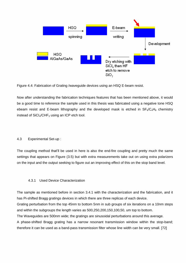
Figure 4.4: Fabrication of Grating /waveguide devices using an HSQ E-beam resist.
Now after understanding the fabrication techniques features that has been mentioned above, it would
be a good time to reference the sample used in this thesis was fabricated using a negative tone HSQ
ebeam resist and E-beam lithography and the developed mask is etched in SF6/C4H8 chemistry
instead of SiCI4/CHF3 using an ICP etch tool.
4.3 Experimental Set-up :
The coupling method that‘ll be used in here is also the end-fire coupling and pretty much the same
settings that appears on Figure (3.5) but with extra measurements take out on using extra polarizers
on the input and the output seeking to figure out an improving effect of this on the stop band level.
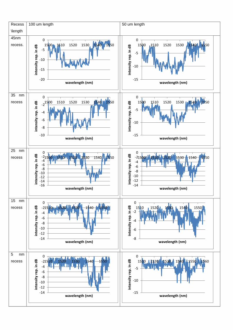
4.3.1 Used Device Characterization
The sample as mentioned before in section 3.4.1 with the characterization and the fabrication, and it
has Pi-shifted Bragg gratings devices in which there are three replicas of each device.
Grating perturbation from the top 45nm to bottom 5nm in sub groups of six iterations on a 10nm steps
and within the subgroups the length varies as 500,250,200,150,100,50, um top to bottom.
The Waveguides are 500nm wide; the gratings are sinusoidal perturbations around this average.
A phase-shifted Bragg grating has a narrow resonant transmission window within the stop-band;
therefore it can be used as a band-pass transmission filter whose line width can be very small. [72]

4.3.2 Results and Discussion
As a start in the next three pages table a general graphs that summarize the behavior of the used
device sweeping over the variation of the perturbations and the lengths will be shown, considering that
all of the measurements have taken a place on using polarizer rotator which been set to filter out the
TM mode on the input and same in the output.
The laser sweeping process took a place over the grating on a wavelength span from 1500 nm to
1560 nm, and it shall be noticeable that the scale on the wavelength is changing considering the
behavior of the stop-band itself.
The resolution of the sweeping was 0.1 nm, and it should be mentioned in here that this resolution is
not the best resolution to show the exact behavior of the grating but to perform this process over
nearly a 90 device and as time consuming it would‘ve been this resolution was the most appropriate.
In all cases it‘s supposed to be resulted as a stop-band filter over the variable lengths and
perturbations but they‘ll differ by the amount of stop-band level and the amount of noise fluctuations
on the stop-band floor.
The cardinal concept here is to find a stop band that will be low and smooth as much as possible
because the stop-band floor level and the noise fluctuations on the band will explain the occurred loss
would be caused whether by the modal interact before the grating device or by the scattering on the
device itself.
Recess
\length
500 um length 250 um length
45nm
recess.
35 nm
recess
25 nm
recess
15 nm
recess
5 nm
recess
-15
-10
-5
0
1500 1520 1540
inte
nsi
ty r
ep
. in
dB
wavelength(nm) -14
-12
-10
-8
-6
-4
-2
0
1500 1510 1520 1530 1540 1550
inte
nsi
ty r
ep
. in
dB
wavelength(nm)
-18-16-14-12-10-8-6-4-20
1500 1520 1540
inte
nsi
ty r
ep
. in
dB
wavelength (nm) -16-14-12-10-8-6-4-20
1500 1510 1520 1530 1540 1550
inte
nsi
ty r
ep
. in
dB
wavelength (nm)
-15
-10
-5
0
1510 1520 1530 1540 1550
inte
nsi
ty r
ep
. in
dB
wavelength (nm) -15
-10
-5
0
1510 1520 1530 1540 1550
inte
nsi
ty r
ep
. in
dB
wavelength (nm)
-16-14-12-10-8-6-4-20
1510 1520 1530 1540 1550
inte
nsi
ty r
ep
. in
dB
wavelength (nm) -15
-10
-5
0
1510 1520 1530 1540 1550
inte
nsi
ty r
ep
. in
dB
wavelength (nm)
-16-14-12-10-8-6-4-20
1510 1530 1550
inte
nsi
ty r
ep
. in
dB
wavelength (nm) -20-18-16-14-12-10-8-6-4-20
1510 1528 1546
inte
nsi
ty r
ep
. in
dB
wavelength (nm)

Recess
\length
200 um length 150 um length
45nm
recess.
35 nm
recess
25 nm
recess
15 nm
recess
5 nm
recess
-12
-10
-8
-6
-4
-2
0
1500 1510 1520 1530 1540 1550
inte
nsi
ty r
ep
. in
dB
wavelength (nm) -16
-14
-12
-10
-8
-6
-4
-2
0
1500 1510 1520 1530 1540 1550
inte
nsi
ty r
ep
. in
dB
wavelength (nm)
-15
-10
-5
0
1500 1520 1540
inte
nsi
ty r
ep
. in
dB
wavelength (nm)
-16-14-12-10-8-6-4-20
1505 1515 1525 1535 1545
inte
nsi
ty r
ep
. in
dB
wavelength (nm)
-18-16-14-12-10-8-6-4-20
1510 1520 1530 1540 1550
inte
nsi
ty r
ep
. in
dB
wavelength (nm) -14
-12
-10
-8
-6
-4
-2
0
1505 1515 1525 1535 1545
inte
nsi
ty r
ep
. in
dB
wavelength (nm)
-16-14-12-10-8-6-4-20
1510 1520 1530 1540 1550
inte
nsi
ty r
ep
. in
dB
wavelength (nm) -18-16-14-12-10-8-6-4-20
1515 1525 1535 1545 1555
inte
nsi
ty r
ep
. in
dB
wavelength (nm)
-16-14-12-10-8-6-4-20
1520 1530 1540 1550 1560
inte
nsi
ty r
ep
. in
dB
wavelength (nm) -16-14-12-10-8-6-4-20
1520 1530 1540 1550 1560
inte
nsi
ty r
ep
. in
dB
wavelength (nm)
Recess
\length
100 um length 50 um length
45nm
recess.
35 nm
recess
25 nm
recess
15 nm
recess
5 nm
recess
-20
-15
-10
-5
0
1500 1510 1520 1530 1540 1550
inte
nsi
ty r
ep
. in
dB
wavelength (nm) -15
-10
-5
0
1500 1510 1520 1530 1540 1550
inte
nsi
ty r
ep
. in
dB
wavelength (nm)
-10
-8
-6
-4
-2
0
1500 1510 1520 1530 1540 1550
inte
nsi
ty r
ep
. in
dB
wavelength (nm) -15
-10
-5
0
1500 1510 1520 1530 1540 1550
inte
nsi
ty r
ep
. in
dB
wavelength (nm)
-16-14-12-10-8-6-4-20
1500 1510 1520 1530 1540 1550
inte
nsi
ty r
ep
. in
dB
wavelength (nm) -14-12-10-8-6-4-20
1500 1510 1520 1530 1540 1550
inte
nsi
ty r
ep
. in
dB
wavelength (nm)
-14
-12
-10
-8
-6
-4
-2
0
1510 1520 1530 1540 1550
inte
nsi
ty r
ep
. in
dB
wavelength (nm) -8
-6
-4
-2
0
1510 1520 1530 1540 1550
inte
nsi
ty r
ep
. in
dB
wavelength (nm)
-14
-12
-10
-8
-6
-4
-2
0
1510 1520 1530 1540 1550
inte
nsi
ty r
ep
. in
dB
wavelength (nm) -15
-10
-5
0
1510 1520 1530 1540 1550 1560
inte
nsi
ty r
ep
. in
dB
wavelength (nm)

Table 4.1 SOI Bragg Grating characterization of variable recesses with different lengths.
Noticeable points on the used SOI Bragg Grating devices behavior are summarized below:
1- The stop-band widths increasing when the recess is big and that‘s logical because with a
strong Λ factor it means a strong perform on the reflection.
As a practical example for the point above, for the 500 um grating length the behavior goes as
follow when the recesses goes down: 45 nm gives a band width of 19 nm , for 25 nm length it
gives an 11.8 nm width and finally for the 5 nm recess it gives 6.4 nm.
2- As a follow up on the point before the stop-band width is nearly the same for all the lengths on
a specific grating perturbation, which means that when the grating recess is 45 nm no matter
what the length is, the bandwidth is nearly around the 19 nm, for the 25 nm is around 11 nm
and for the 5 nm recess is around 6 nm band width and so on.
3- The notch (gap-mode) that identifies the phase shifting in the grating in the large lengths ‗‘
500,250,200 ‗‘ will be hard to notice for the reason of that the notch width might get so narrow
and it would be hard for it to appear on a sweeping of 0.1 nm or even for the .01 nm resolution.
Also for the reason that the recess was so strong that might reflect the notch on that
wavelength and appears as part of the loss.
4- The stop-band floor which was the focus of interest is noticeably lower in the smaller
perturbation and that happens for the reasons of: the amount of reflection occurs on the grating
is low in the grating when the perturbation is small which makes the scattered light in the
grating is and that lowers the possibility of getting an extra TM polarization on the output, and
sure when that happen it makes the stop-band smoother and easier to be observed.
5- In the so small grating more specifically the 50 nm with a smaller recess that the floor of the
stop-band becomes more fluctuated and again as shown in section three of the third chapter
that it would be the effect of the scattering light inside the waveguide.
-8
-7
-6
-5
-4
-3
-2
-1
0
1510 1530 1550
inte
nsi
ty r
ep
. in
dB
wavelength (nm) -12
-10
-8
-6
-4
-2
0
1510 1520 1530 1540 1550 1560
inte
nsi
ty r
ep
. in
dB
wavelength (nm)
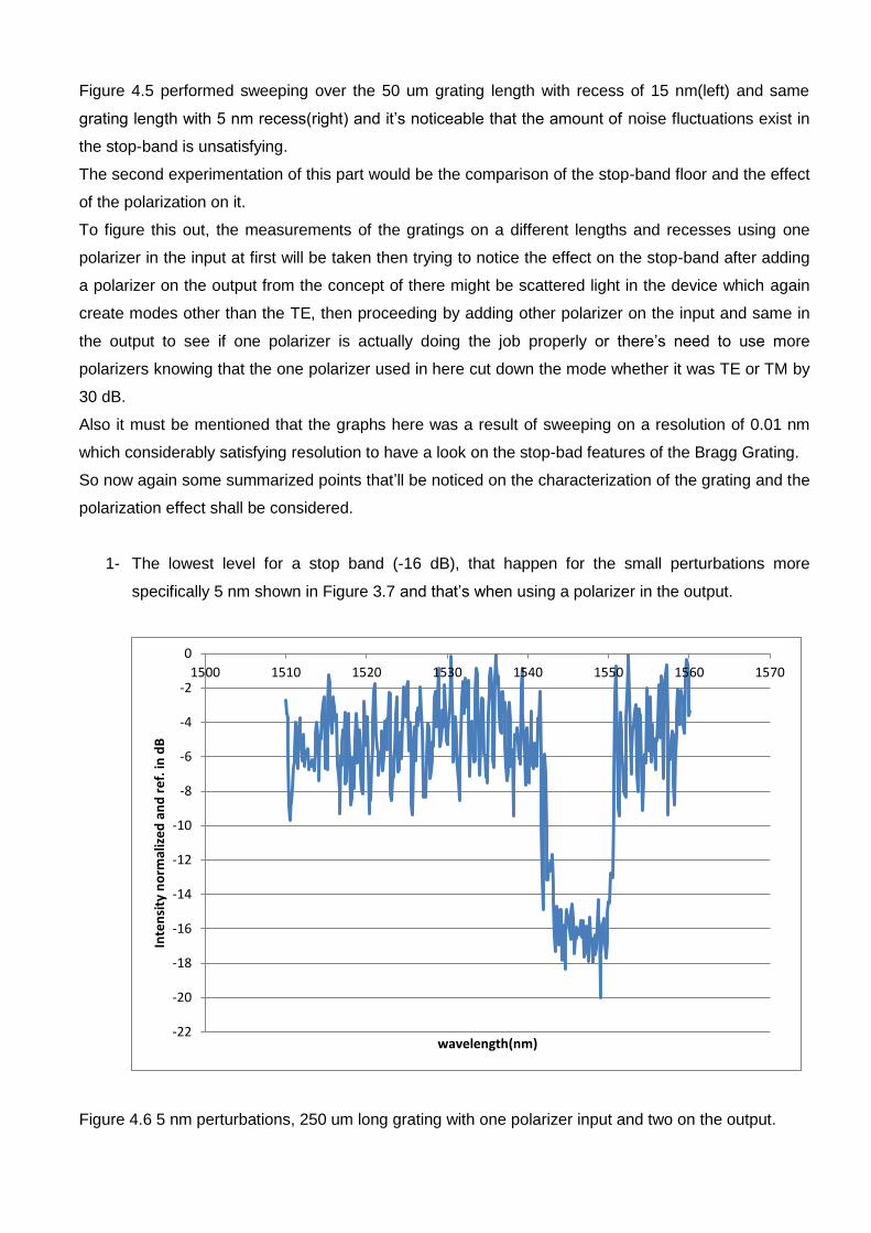
Figure 4.5 performed sweeping over the 50 um grating length with recess of 15 nm(left) and same
grating length with 5 nm recess(right) and it‘s noticeable that the amount of noise fluctuations exist in
the stop-band is unsatisfying.
The second experimentation of this part would be the comparison of the stop-band floor and the effect
of the polarization on it.
To figure this out, the measurements of the gratings on a different lengths and recesses using one
polarizer in the input at first will be taken then trying to notice the effect on the stop-band after adding
a polarizer on the output from the concept of there might be scattered light in the device which again
create modes other than the TE, then proceeding by adding other polarizer on the input and same in
the output to see if one polarizer is actually doing the job properly or there‘s need to use more
polarizers knowing that the one polarizer used in here cut down the mode whether it was TE or TM by
30 dB.
Also it must be mentioned that the graphs here was a result of sweeping on a resolution of 0.01 nm
which considerably satisfying resolution to have a look on the stop-bad features of the Bragg Grating.
So now again some summarized points that‘ll be noticed on the characterization of the grating and the
polarization effect shall be considered.
1- The lowest level for a stop band (-16 dB), that happen for the small perturbations more
specifically 5 nm shown in Figure 3.7 and that‘s when using a polarizer in the output.
Figure 4.6 5 nm perturbations, 250 um long grating with one polarizer input and two on the output.
-22
-20
-18
-16
-14
-12
-10
-8
-6
-4
-2
0
1500 1510 1520 1530 1540 1550 1560 1570
Inte
nsi
ty n
orm
aliz
ed
an
d r
ef.
in d
B
wavelength(nm)
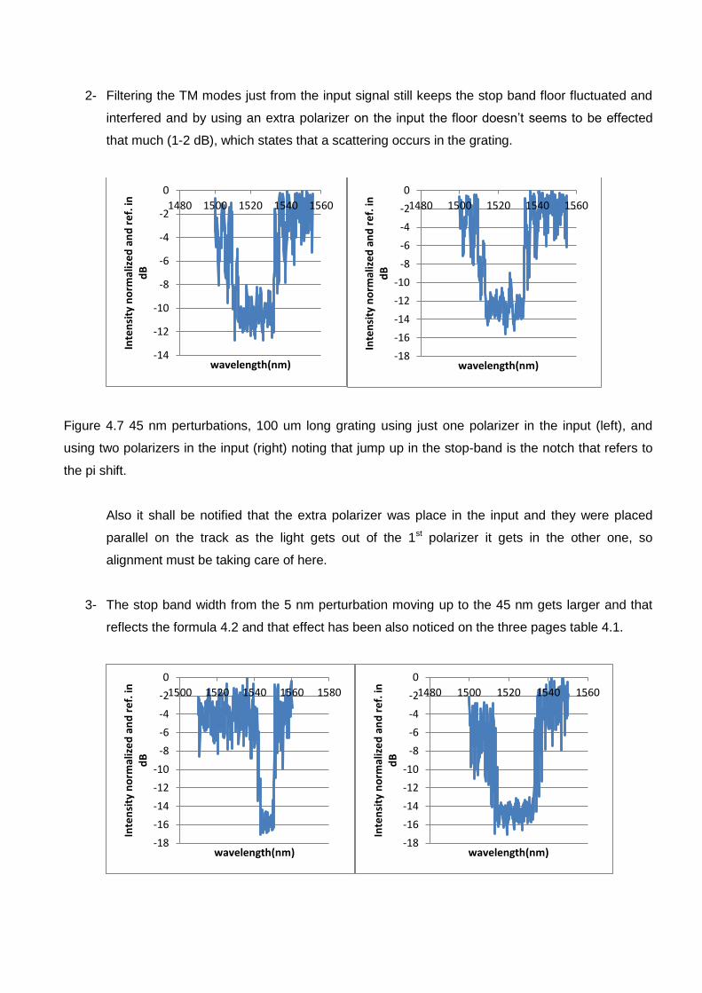
2- Filtering the TM modes just from the input signal still keeps the stop band floor fluctuated and
interfered and by using an extra polarizer on the input the floor doesn‘t seems to be effected
that much (1-2 dB), which states that a scattering occurs in the grating.
Figure 4.7 45 nm perturbations, 100 um long grating using just one polarizer in the input (left), and
using two polarizers in the input (right) noting that jump up in the stop-band is the notch that refers to
the pi shift.
Also it shall be notified that the extra polarizer was place in the input and they were placed
parallel on the track as the light gets out of the 1st polarizer it gets in the other one, so
alignment must be taking care of here.
3- The stop band width from the 5 nm perturbation moving up to the 45 nm gets larger and that
reflects the formula 4.2 and that effect has been also noticed on the three pages table 4.1.
-14
-12
-10
-8
-6
-4
-2
0
1480 1500 1520 1540 1560
Inte
nsi
ty n
orm
aliz
ed
an
d r
ef.
in
dB
wavelength(nm) -18
-16
-14
-12
-10
-8
-6
-4
-2
0
1480 1500 1520 1540 1560
Inte
nsi
ty n
orm
aliz
ed
an
d r
ef.
in
dB
wavelength(nm)
-18
-16
-14
-12
-10
-8
-6
-4
-2
0
1500 1520 1540 1560 1580
Inte
nsi
ty n
orm
aliz
ed
an
d r
ef.
in
dB
wavelength(nm) -18
-16
-14
-12
-10
-8
-6
-4
-2
0
1480 1500 1520 1540 1560
Inte
nsi
ty n
orm
aliz
ed
an
d r
ef.
in
dB
wavelength(nm)
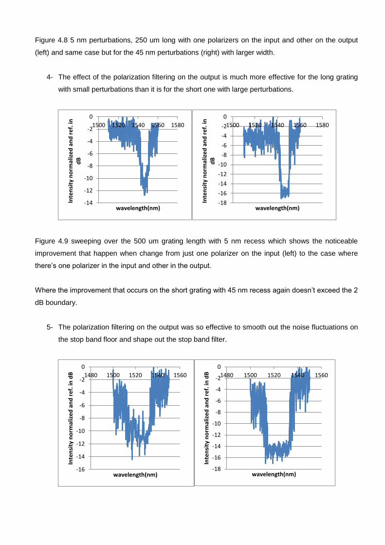
Figure 4.8 5 nm perturbations, 250 um long with one polarizers on the input and other on the output
(left) and same case but for the 45 nm perturbations (right) with larger width.
4- The effect of the polarization filtering on the output is much more effective for the long grating
with small perturbations than it is for the short one with large perturbations.
Figure 4.9 sweeping over the 500 um grating length with 5 nm recess which shows the noticeable
improvement that happen when change from just one polarizer on the input (left) to the case where
there‘s one polarizer in the input and other in the output.
Where the improvement that occurs on the short grating with 45 nm recess again doesn‘t exceed the 2
dB boundary.
5- The polarization filtering on the output was so effective to smooth out the noise fluctuations on
the stop band floor and shape out the stop band filter.
-14
-12
-10
-8
-6
-4
-2
0
1500 1520 1540 1560 1580
Inte
nsi
ty n
orm
aliz
ed
an
d r
ef.
in
dB
wavelength(nm) -18
-16
-14
-12
-10
-8
-6
-4
-2
0
1500 1520 1540 1560 1580
Inte
nsi
ty n
orm
aliz
ed
an
d r
ef.
in
dB
wavelength(nm)
-16
-14
-12
-10
-8
-6
-4
-2
0
1480 1500 1520 1540 1560
Inte
nsi
ty n
orm
aliz
ed
an
d r
ef.
in d
B
wavelength(nm) -18
-16
-14
-12
-10
-8
-6
-4
-2
0
1480 1500 1520 1540 1560
Inte
nsi
ty n
orm
aliz
ed
an
d r
ef.
in d
B
wavelength(nm)
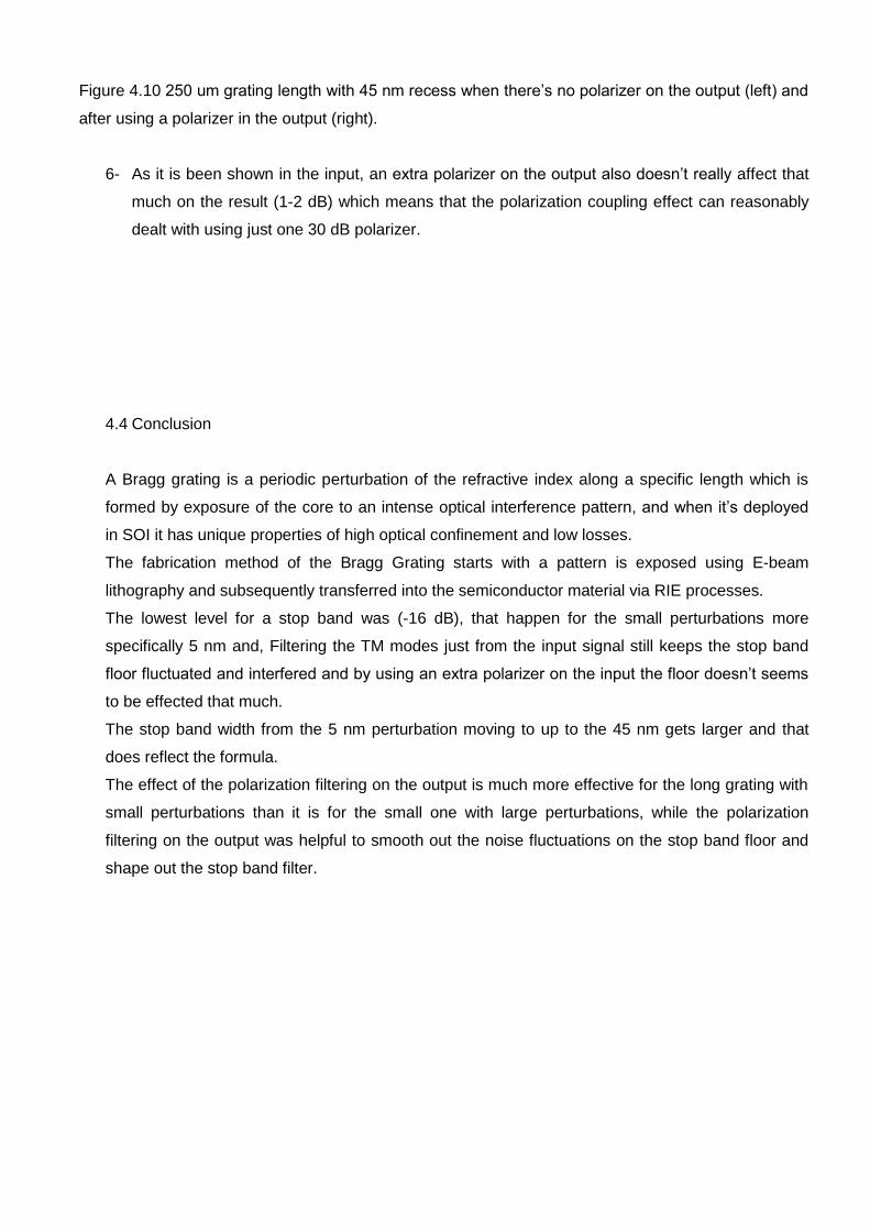
Figure 4.10 250 um grating length with 45 nm recess when there‘s no polarizer on the output (left) and
after using a polarizer in the output (right).
6- As it is been shown in the input, an extra polarizer on the output also doesn‘t really affect that
much on the result (1-2 dB) which means that the polarization coupling effect can reasonably
dealt with using just one 30 dB polarizer.
4.4 Conclusion
A Bragg grating is a periodic perturbation of the refractive index along a specific length which is
formed by exposure of the core to an intense optical interference pattern, and when it‘s deployed
in SOI it has unique properties of high optical confinement and low losses.
The fabrication method of the Bragg Grating starts with a pattern is exposed using E-beam
lithography and subsequently transferred into the semiconductor material via RIE processes.
The lowest level for a stop band was (-16 dB), that happen for the small perturbations more
specifically 5 nm and, Filtering the TM modes just from the input signal still keeps the stop band
floor fluctuated and interfered and by using an extra polarizer on the input the floor doesn‘t seems
to be effected that much.
The stop band width from the 5 nm perturbation moving to up to the 45 nm gets larger and that
does reflect the formula.
The effect of the polarization filtering on the output is much more effective for the long grating with
small perturbations than it is for the small one with large perturbations, while the polarization
filtering on the output was helpful to smooth out the noise fluctuations on the stop band floor and
shape out the stop band filter.
References:
[1] Integrated Optics Theory and Technology Sixth Edition Robert G. Hunsperger Department of
Electrical Engineering University of Delaware
[2] Zaho J.H. - Madsen C.K. - Optical Filter Design and Analysis A Signal Processing Approach (Wiley
1999)
[3] Theory of dielectric waveguides, in Integrated Optics, T. Tamir (ed.), 2nd ed.,Topics Appl. Phys.,
Vol. 7 (Springer, Berlin, Heidelberg 1979) Chap. 2
[4] Basic Geometrical Optics Leno S. Pedrotti ,CORD : Waco, Texas
[5] Part of the lecture materials were adopted from powerpoint slides of Gerd Keiser‘s book 2010,
Copyright © The McGraw-Hill Companies, Inc
[6] Fabrication methods of planar waveguides and related structures ,Sergiusz Patela, Wrocław
University of Technology http://www.patela.prv.pl
[7] R. Olshansky, ―Propagation in glass optical waveguides,‖ Rev. Mod. Phys., vol. 51, no. 2, p. P341,
1979.
[8] Silicon Photonics Waveguides, Prepared by Prof. Graham T. Reed,G. Mashanovich, M. Milosevic,
and F. Gardes ; University of Surrey, Guildford, UK ;Silicon Photonics –PhD course prepared within
FP7-224312 Helios project
[9] Silicon Photonics Waveguides Prepared by Prof. Graham T. Reed,G. Mashanovich, M. Milosevic,
and F. Gardes University of Surrey, Guildford, UK ; for Helios .
[10] G. Pandraud, H.T.M. Pham, P.J. French, P.M. Sarro: PECVD SiC optical waveguide loss and
mode characteristics, Opt. Laser Technol. 39, 532 (2007)
[11] D. Marcuse: Bell Syst. Tech. J. 48, 3187 (1969)
[12] E.A.J. Marcatili, S.E. Miller: Bell Syst. Tech. J. 48, 2161 (1969)
[13] Gnan - PhD (2007) - University of Glasgow - Photonic Wire Devices in Silicon-On-Insulator
[13] Alt. Ref. ‗‘ http://ioptic.wordpress.com/2011/01/12/cut-back-method-for-testing-fibre-loss/ ‗‘
[14] Optical Interconnects: The Silicon Approach by Lorenzo Pavesi, Gérard Guillot
[15] Fabry, C., and A. Perot, Theorie et applications d'une nouvelle methode de spectroscopie
interferentielle. Ann. Chim. Phys. 16: 115 (1899).
[16] http://physics.usask.ca/~angie/ep421/lab3/theory.htm
[17] Confocal Fabry-Perot Cavity ; Seung-Hyun Lee ; SUNY at Stony Brook ; Optics Rotation Project
for Fall 2001
[18] Max Born & Emil Wolf Principles of Optics ( 4th.ed.) Pergamon Press 1970
[19] CHARACTERISATION OF SILICON PHOTONICS DEVICES BY David M. H. LEUNG
A THESIS SUBMITTED FOR THE DEGREE OF DOCTOR OF PHILOSOPHY AT CITY UNIVERSITY
LONDON PHOTONICS MODELLING GROUP SCHOOL OF ENGINEERING AND MATHEMATICAL
SCIENCES NORTHAMPTON SQUARE, LONDON EC1V 0HB
UNITED KINGDOM JANUARY 2013 ( Fig. 4.8. The variations of neff, (a) with W for quasi-TE modes
with different H,)
[20] November 15,1990 / Vol. 15, No. 22 / OPTICS LETTERS ; D. F. Clark and M. S. Iqbal
Department of Electronic and Electrical Engineering, University of Strathclyde, 204 George Street,
Glasgow GI 1XW, Scotland, UK
[21] waveguide losses and input-output coupling , End-Fire Coupling to Waveguides of Different
Length , university of Washington
[22] Wavelength Tunable Laser Diode source Tunics PR/PRI Manual
[23] Guidance on the Safe use of lasers in education and research , AURPO 2006 edition
[24] Model 5209 single phase lock-in amplifier instruction manual
[25] Celler, G. K.; Cristoloveanu, S. (2003). "Frontiers of silicon-on-insulator". J Appl Phys 93 (9):
4955.doi:10.1063/1.1558223.
[26] Marshall, Andrew; Natarajan, Sreedhar (2002). SOI design: analog, memory and digital
techniques. Boston: Kluwer. ISBN 0792376404.
[27] http://www-03.ibm.com/press/us/en/pressrelease/2521.wss
[28] http://asmddc.hanyang.ac.kr/
[29] http://asmddc.hanyang.ac.kr/ ‗‘what is SOI? ‗‘
[30] White Paper On Silicon On Insulator (SOI) Implementation June 2009 by Narayana Murty Kodeti ;
Infotech Enterprises Ltd.,
[31] Smart Cut™ A guide to the technology, the process, the products By George Celler, Chief
Scientist and Michael Wolf, Sr. VP, Sales & Marketing SOITEC
[32] "SemiConductor Wafer Bonding: Science and Technology" by Q.-Y. Tong & U. Gösele, Wiley-
Interscience, 1998, ISBN 978-0-471-57481-1
[33] Silicon on Insulator ; Advanced Electronic Devices by Karthik Swaminathan
[34] R. C. Frye, J. E. Griffith, and Y. H. Wong, US Patent No. 4,501,060 ~26 February 1985!.
[35] www.soitec.com/pdf/Soitec_SmartCut
[36] http://www.sigen.net/
[37] ELTRAN - Novel SOI Wafer Technology, JSAPI vol.4
[38] http://homepage.ntu.edu.tw
[39] the effect of nitrogen implantation doses on the structure of separation by implantation of oxygen
and nitrogen Authors : Enxia Zhang and Wanbing Yi and Jing Chen and Zhengxuan Zhang and Xi
WangYear
[40] Silicon-on-insulator; SOI technology and ecosystem Emerging SOI applications by Horacio
Mendez ; Executive Director of the SOI Industry Consortium ; April 9, 2009
[41] K. O. Hill, Y. Fujii, D. C. Johnson, and B. S. Kawasaki, ―Photosensitivity in optical fiber
waveguides: Application to reflection filter fabrication,‖ Appl. Phys. Lett., vol. 32, pp. 647–649, 1978
[42] B. S. Kawasaki, K. O. Hill, D. C. Johnson, and Y. Fujii, ―Narrow-band Bragg reflectors in optical
fibers,‖ Opt. Lett., vol. 3, pp. 66–68, 1978

[43] T. E. Murphy, J. T. Hastings, and H. I. Smith, ―Fabrication and characterization of Narrow-band
Bragg-reflection filters in silicon-on insulator ridge waveguides,‖ J. Lightwave Technol., vol. 19, no. 12,
pp. 1938–1942, 2001.
[44] S. Homampour, M. P. Bulk, P. E. Jessop, and A. P. Knights, ―Thermal tuning of planar Bragg
gratings in silicon-on-insulator rib waveguides,‖ Phys. Status Solidi C, no. S1, pp. S240–S243, 2009.
[45] T. E. Murphy, J. T. Hastings, and H. I. Smith, ―Fabrication and characterization of narrow-band
Bragg-reflection filters in silicon-oninsulator ridge waveguides,‖ J. Lightwave Technol., vol. 19, no. 12,
pp. 1938–1942, 2001.
[46] J. T. Hastings, M. H. Lim, J. G. Goodberlet, and H. I. Smith, ―Optical waveguides with apodized
sidewall gratings via spatial-phase-locked electron-beam lithography,‖ J. Vac. Sci. Technol. B, vol. 20,
no. 6, pp. 2753–2757, 2002.
[47] A. S. Jugessur, J. Dou, J. S. Aitchison, R. M. De La Rue, and M. Gnan, ―A photonic nano-Bragg
grating device integrated with microfluidic channels for bio-sensing Applications,‖ Microelectronic
Engineering, vol. 86, no. 4-6, pp. 1488–1490, 2009.
[48] D. T. H. Tan, K. Ikeda, and Y. Fainman, ―Cladding-modulated Bragg gratings in silicon
waveguides,‖ Opt. Lett., vol. 34, no. 9, pp. 1357–1359, 2009.
[49] X. Wang, W. Shi, R. Vafaei, N. A. F. Jaeger, and L. Chrostowski,
―Silicon-on-insulator Bragg gratings fabricated by deep UV lithography,‖ in IEEE Asia Communications
and Photonics Conf., 12/2010 2010.
[50] D. K. W. Lam and B. K. Garside, ―Characterization of single-mode optical fiber filters,‖ Appl. Opt.,
vol. 20, pp. 440–445, 1981.
[51] CHARACTERIZATION OF FIBER BRAGG GRATINGS FOR TEMPERATURE SENSING
APPLICATIONS ;Arun Venkataraman ;Purnima Vuggina ; Sreelakshmi Talluri
[52] A. G. Rickman, G. T. Reed and F. Namavar, ―Silicon-on-insulator optical rib waveguide loss and
mode characteristics,‖ Journal of Lightwave Technology, Vol.12, pp.1771-1776, 1994. 6. Beam Prop,
by RSoft research software.
[53] X. Wang, W. Shi, R. Vafaei, N. A. F. Jaeger, and L. Chrostowski, ―Silicon-on-insulator Bragg
gratings fabricated by deep UV lithography,‖ in IEEE Asia Communications and Photonics Conf.,
12/2010 2010.
[54] K. O. Hill, Y. Fujii, D. C. Johnson, and B. S. Kawasaki, ―Photosensitivity in optical fiber
waveguides: Application to reflection filter fabrication,‖ Appl. Phys. Lett., vol. 32, pp. 647–649, 1978.
[55] G. Meltz, W. W. Morey, and W. H. Glenn, ―Formation of Bragg gratings in optical fibers by a
transverse holographic method,‖ Opt. Lett., vol. 14, pp. 823–825, 1989.
[56] K. O. Hill, B. Malo, F. Bilodeau, D. C. Johnson, and J. Albert, ―Bragg gratings fabricated in
monomode photosensitive optical fiber by UV exposure through a phase mask,‖ Appl. Phys. Lett., vol.
62, pp. 1035–1037, 1993.
[57] D. Z. Anderson, V. Mizrahi, T. Erdogan, and A. E. White, ―Production of in-fiber gratings using a
diffractive optical element,‖ Electron. Lett., vol. 29, pp. 566–568, 1993.
[58] E. Meyer, D. Basting: Eximer-laser advances aid production of fiber gratings. Laser Focus World
36, 107 (April 2000)
[59] Meltz G., Morey W. W., and Glenn W. H., "Formation of Bragg gratings in optical fibres by
transverse holographic method," Opt. Lett. 14(15), 823 (1989).
[60] Lerner J. M., Flamand J., Laude J. P., Passereau G., and Thevenon A., "Diffraction gratings ruled
and holographic — a review," in Proc. ofSPIE Symposium on Periodic Structures, Gratings, Moire
Patterns, and Diffraction Phenomenon, vol. 240, pp. 82-88 (1980).
[61] A. Othonos and K. Kyriac, Fiber Bragg Gratings. Artech House, 1999.
[62] Fiber Bragg Grating Technology Fundamentals and Overview Kenneth O. Hill and Gerald Meltz,
Member, IEEE JOURNAL OF LIGHTWAVE TECHNOLOGY, VOL. 15, NO. 8, AUGUST 1997
[63] K. O. Hill, ―Aperiodic distributed-parameter waveguides for integrated optics,‖ Appl. Opt., vol. 13,
pp. 1853–1856, 1974.
[64] Fabrication of Phase-Shifted Fiber Bragg Gratings for Biosensing Applications Qi Zhang Fawen
Guo Thomas Fink Ming Han Department of Electrical Engineering, University of Nebraska-Lincoln
[65] B. Malo, K. O. Hill, F. Bilodeau, D. C. Johnson, and J. Albert, ―Point-by point fabrication of micro-
Bragg gratings in photosensitive fiber using single excimer pulse refractive index modification
techniques,‖ Electron. Lett., vol. 29, pp. 1668–1669, 1993.
[66] Fiber Bragg Gratings: fundamentals and applications Patrice Mégret Sébatien Bette Cathy
Crunelle Christophe Caucheteur 3rd May 2007
[67] M. Y. Lie, S. Y. Chou, ―High modulation depth and short cavity length silicon Fabry-Perot
modulator with two grating Bragg reflectors,‖ Applied Physics Letters, Vol. 68, No. 2, pp.170-172,
1996.
[68] A. Cutolo, M. Iodice, A. Irace, P. Spirito, L. Zeni, ―An electrically controlled Bragg reflector
integrated in a rib silicon on insulator waveguide,‖ Applied Physics Letter, Vol.71, No. 2, pp. 199-201,
1997.
[69]T. E. Murphy, J. T. Hastings, H. I. Smith, ―Fabrication and characterization of narrow band Bragg
reflection filters in Silicon-on-insulator ridge waveguides‖, Journal of Lightwave Technology, Vol.19,
No.12, pp.1938-1942, 2001.
[70] T. Aalto, S. Yliniemi, R. Heimala, P. Pekko, J. Simonen and M. Kuittinen, ―Integrated Bragg
gratings in silicon-on insulator waveguides,‖ Proceedings of SPIE Vol. 4640, Photonics West 2002,
Integrated Optics: Devices, Materials and Technologies VI, pp.117-124, 2002.
[71] JOURNAL OF LIGHTWAVE TECHNOLOGY, VOL. 15, NO. 8, AUGUST 1997 Fiber Bragg
Grating Technology Fundamentals and Overview Kenneth O. Hill and Gerald Meltz, Member, IEEE
[72] G. P. Agrawal, et. al., IEEE Photon. Technol. Lett., vol. 6, no. 8, pp. 995-997 (1994)
[73] J.-F. Cliche, Y. Painchaud, C. Latrasse, M.-J. Picard, I. Alexandre and M. Têtu, ―Ultra-narrow
Bragg grating for active semiconductor laser linewidth reduction through electrical feedback,‖ Proc. of
BGPP‘07, paper BTuE2 (2007).
[74] Y. Painchaud, M. Poulin, C. Latrasse, N. Ayotte, M.-J. Picard and M. Morin, ―Bragg grating notch
filters in silicon-on-insulator waveguides,‖ accepted for BGPP‘12.
[75] P. Dumon, W. Bogaerts, V. Wiaux, J. Wouters, S. Beckx, J. van Campenhout, D. Taillaert, B.
Luyssaert, P. Bienstman, D. van Thourhout and R. Baets, ―Low-loss SOI photonic wires and ring
resonators fabricated with deep UV lithography,‖ IEEE Photon. Technol. Lett., Vol.16 (5) p.1328
(2004).
[76] Fabrication of Micro-optics in Polymers and in UV Transparent materials ; G Kopitkovas, L. Urech
and T.Lippert
[77] Bohren,C. F. and Huffman, D.R. "Absorption and Scattering of Light by Small Particles", Wiley,
(1983), isbn= 0-471-29340-7
[78] http://www.ad-net.com.tw/index.php?id=472
[79] Trevor S. Bird, "Definition and Misuse of Return Loss", IEEE Antennas & Propagation Magazine,
vol.51, iss.2, pp.166-167, April 2009.
[80] Optical Excitation of Electromagnetic Modes Using Grating Couplers by Guy Peter Bryan/Brown
University of Exeter
[81] Guiding, Modulating, and Emitting Light on Silicon—Challenges and Opportunities; Michal Lipson,
IEEE JOURNAL OF LIGHTWAVE TECHNOLOGY, VOL. 23, NO. 12, DECEMBER 2005.
[82] Excitation of short-wavelength spin waves in magnonic waveguides by V. E. Demidov, M. P.
Kostylev, K. Rott, J. Mu¨nchenberger, G. Reiss, and S. O. Demokritov; App Phy Jour Accepted 10
August 2011; published 25 August 2011
[83] http://www.microwaves101.com/encyclopedia/TEM.cfm
[84] Rectangular Waveguides; Dr. S. Cruz-Pol; INEL 6216; University of Puerto Rico; Mayagüez
[85] M. Y. Lie, S. Y. Chou, ―High modulation depth and short cavity length silicon Fabry-Perot
modulator with two grating Bragg reflectors,‖ Applied Physics Letters, Vol. 68, No. 2, pp.170-172,
1996.
[86] A. Cutolo, M. Iodice, A. Irace, P. Spirito, L. Zeni, ―An electrically controlled Bragg reflector
integrated in a rib silicon on insulator waveguide,‖ Applied Physics Letter, Vol.71, No. 2, pp. 199-201,
1997.
[87] T. E. Murphy, J. T. Hastings, H. I. Smith, ―Fabrication and characterization of narrow band Bragg
reflection filters in Silicon-on-insulator ridge waveguides‖, Journal of Lightwave Technology, Vol.19,
No.12, pp.1938-1942, 2001.
[88] T. Aalto, S. Yliniemi, R. Heimala, P. Pekko, J. Simonen and M. Kuittinen, ―Integrated Bragg
gratings in silicon-oninsulator waveguides,‖ Proceedings of SPIE Vol. 4640, Photonics West 2002,
Integrated Optics: Devices, Materials and Technologies VI, pp.117-124, 2002.
[89] L. C. Kimerling, "Silicon microphotonics", Applied Surface Science, vol. 159, pp. 8−13, 2000.
[90] R. A. Soref, "Silicon-Based Optoelectronics", Proceedings of the IEEE, vol. 81, no. 12, pp.
1687−1706, 1993.
[91] Canciamilla - PhD (2010) - Politecnico di Milano - Slow Light Structure for Optical Signal
Processing
[92] T. Tsuchizawa, K. Yamada, H. Fukuda, T. Watanabe, J. Takahashi, M. Takahashi, T. Shoji, E.
Tamechika, S. Itabashi and H. Morita, "Microphotonics Devices Based on Silicon Microfabrication
Technology", IEEE J. Sel. Topics in Quantum Electron., vol. 11, no. 1, pp. 232-240, Jan./Feb. 2005.
[93] C.G. Poulton, C. Koos, M. Fujii, A. Pfrang, T. Schimmel, J. Leuthold, W. Freude, "Radiation
modes and roughness loss in high index-contrast waveguides", IEEE J. Sel. Topics in Quantum
Electron., vol. 16, pp. 1306−1321, 2006.
[94] A. Liu, R. Johnes, L. Liao, D. Samara-Rubio, D. Rubin, O. Chohen, R. Nicolaescu and M.
Paniccia, "A high-speed silicon optical modulation based on a metal-oxide-semiconductor capacitor",
Nature, vol. 427, pp. 615−618, 2004.
[95] F. Xia, L. Sekaric and Y. Vlasov, "Ultracompact optical buffers on a silicon chip", Nature
Photonics, vol. 1, pp. 65-71, 2006.
[97] N. Sherwood-Droz, H. Wang, L. Chen, B. G. Lee, A. Biberman, K. Bergman and M. Lipson,
"Optical 4x4 hitless silicon router for optical Networks-on-Chip (NoC)", Optics Express, vol. 16, no. 20,
Sept. 2008.
[96] T. Fukazawa, F. Ohno, and T. Baba, "Very compact arrayedwaveguide- grating demultiplexer
using Si photonic wire waveguides", Jpn. J. Appl. Phys., vol. 43, no. 5b, pp. 673-675, 2004.
[97] N. Sherwood-Droz, H. Wang, L. Chen, B. G. Lee, A. Biberman, K. Bergman and M. Lipson,
"Optical 4x4 hitless silicon router for optical Networks-on-Chip (NoC)", Optics Express, vol. 16, no. 20,
Sept. 2008.
[98] L. Pavesi, L. Dal Negro, C. Mazzoleni, G. Franzo, and F. Priolo, "Optical gain in silicon
nanocrystals", Nature, vol. 408, no. 6811, pp. 440−444, 2000.
[99] M. Bruel, B. Aspar and H. Auberton, "Smart-cut: A new silicon on insulator material technology
based on hydrogen implantation and wafer bonding", Japanese Journal of Applied Physics, Part 1:
Regular Papers and Short Notes and Review Papers, vol. 36, no. 3 SUPPL.
B, pp. 1636−1641, 1997.
[100] "SOITEC Unibond Process" [Online], available at: http://www.semiconductor-
technology.com/projects/soitecbernin/soitecbernin2.html
[101] H. M. H. Chong, "Photonic Crystal and Photonic Wire Structures for Photonic Integrated
Circuits", Ph.D. dissertation, University of Glasgow, 2004.
[102] E. A. Camargo, "Switchable Devices Based On Photonic Crystal Channel Waveguides", Ph.D.
dissertation, University of Glasgow, 2004.
[103] H. Namatsu, T. Yamaguchi, M. Nagase, K. Yamazaki, and K. Kurihara, "Nano-patterning of a
hydrogen silsesquioxane resist with reduced linewidth fluctuations", Microelectronic Engineering, vol.
41- 42, pp. 331−334, 1998.
[104] P. Rai-Choudhury, "Handbook of Microlithography, Micromachining and Microfabrication", SPIE,
1997, vol. 1: Microlithography.
[105] S. Thoms and D. S. Macintyre, "Tilt-corrected stitching for electron eam lithography",
Microelectronic Engineering, vol. 11, no. 1, pp. 232−239, 2007.
[106] M. Gnan, S. Thoms, D. S. Macintyre, R. M. De La Rue and M. Sorel, "Fabrication of low-loss
photonic wires in Silicon-on-insulator using hydrogen silsesquioxane electron-beam resist", Electronic
Letters, vol. 44, pp. 155, 2008.
[107] W. Bogaerts, V. Wiaux, D. Taillaert, S. Beckx, B. Luyssaert, P. Bienstman, and R. Baets,
―Fabrication of photonic crystals in silicon-on-insulator using 248 − nm deep UV lithography,‖ IEEE
Journal on Selected Topics in Quantum Electronics, vol. 8, no. 4, p. 928, 2002.
[108] Integrated Chirped Bragg Gratings for Dispersion Control by Michael Strain ; November 2007 A
thesis submitted for the degree of Doctor of Philosophy (Ph.D.) to the Faculty of Engineering
Department of Electronics and Electrical Engineering University of Glasgow
[109] M. Settle, M. Salib, A. Michaeli, and T. F. Krauss, ―Low loss silicon on insulator photonic crystal
waveguides made by 193 nm optical lithography,‖ Optics Express, vol. 14, no. 6, p. 2440, 2006.
[110] Vistec, ―Leica VB6 UHR EWF, http://www.vistec-semi.com/,‖ April 2006.
[111] T. Katoh, Y. Nagamune, G. P. Li, S. Fukatsu, Y. Shiraki, and R. Ito, ―Fabrication Of Ultrafine
Gratings On GaAs By Electron-Beam Lithography And 2-Step Wet Chemical Etching,‖ Applied
Physics Letters, vol. 57, no. 12, pp. 1212–1214, 1990.
[112] S. W. Pang, G. A. Lincoln, R. W. McClelland, P. D. Degraff, M. W. Geis, and W. J. Piacentini,
―Effects Of Dry Etching On GaAs,‖ Journal Of Vacuum Science & Technology B, vol. 1, no. 4, pp.
1334–1337, 1983.
[113] S. J. Pearton, U. K. Chakrabarti, W. S. Hobson, and A. P. Kinsella, ―Reactive Ion Etching Of
GaAs, AlGaAs, And GaSb In Cl2 And SiCl4,‖ Journal Of Vacuum Science & Technology B, vol. 8, no.
4, pp. 607–617, 1990.
[114] Albert Michelson, Edward Morley (1887). "On the Relative Motion of the Earth and the
Luminiferous Ether". American Journal of Science 34 (203): 333–345.

Figures and Tables List:
Figure 1.1 The Ray Optics Approach to Describing Planar Waveguides. 3
Figure 1.2 a rectangular waveguide with perfectly conducting walls, filled with a lossless material. 5
Figure 2.1: Sketch of process sequence for fabrication of devices in SOI, as reported in [98]: (a) common four-
steps fabrication process based on intermediate SiO2 layer, (b) two-steps fabrication process based on direct
pattern transfer from HSQ resist. 13
Figure 2.2 a single (out of many devices was planted on the used sample) dimensions of an SOI waveguide.
14
Figure 2.3 Smart Cut is at the heart of Soitec‘s UNIBOND SOI wafer fabrication. In this case, the process is
based on Hydrogen implantation and wafer-bonding to a silicon handle substrate B. 15
Figure 3.1 Electron energy transitions during absorption. 21
Figure 3.2 The Output Spectrum of the Fabry-Perot Resonator. 24
Figure 3.3 Example on Fabry-Perot scanning. 26
Figure 3.4 Experimental set-up for measure. of waveguide attenuation employing endfire coupling. 27
Figure 3.5 Diagram of the Set up used in the experiments. 28
Figure 3.6 Propagation losses for different widths of waveguides. 30
Figure 3.7 Laser sweeping on an 800nm waveguide‘s width. 31
Figure 3.8 TM Percentage to the total output signal (TE+TM). 32
Figure 4.1 first model introduced for Bragg Grating technique on Fiber. 35
Figure 4.2 shows the proposed SOI waveguide with Bragg grating. 36
Figure 4.3: Fabrication procedure for pattern writing in AlGaAs/GaAs using PMMA based E-beam lithography.
40
Figure 4.4: Fabrication of waveguide devices using an HSQ E-beam resist. 41
Table 4.1 SOI Bragg Grating characterization of variable recesses with different lengths. 47
Figure 4.5 performed sweeping over the 50 um grating length with recess of 15 nm(left) and same grating length
with 5 nm recess(right) and it‘s noticeable that the amount of noise fluctuations exist in the stop-band is
unsatisfying. 48
Figure 4.6 5 nm perturbations, 250 um long grating with one polarizer input and two on the output. 49
Figure 4.7 45 nm perturbations, 100 um long grating using just one polarizer in the input (left), and using two
polarizers in the input (right) noting that jump up in the stop-band is the notch that refers to the pi shift.
49
Figure 4.8 5 nm perturbations, 250 um long with one polarizers on the input and other on the output (left) and
same case but for the 45 nm perturbations (right). 50
Figure 4.9 sweeping over the 500 um grating length with 5 nm recess which shows the noticeable improvement
that happen when change from just one polarizer on the input (left) to the case where there‘s one polarizer in the
input and other in the output. 50
Figure 4.10 250 um grating length with 45 nm recess when there‘s no polarizer on the output (left) and after
using a polarizer in the output (right). 51