Embed Size (px)
Citation preview
Characterization of HV-CMOSpixel sensor prototypes
Ettore Zaffaroni
STREAM Final Conference, 17/09/2019
Smart Sensor Technologies and Training for Radiation Enhanced Applications and Measurements (STREAM) is a project funded by the European Commission under the Horizon2020 Framework Program under the Grant Agreement no 675587.
STREAM began in January 2016 and will run for 4 years.
Ettore Zaffaroni 2
Outline
● Introduction● The characterized sensors● TCT (Transient Current Technique)
measurements and results● Testbeam measurements and results
Ettore Zaffaroni 3
Introduction
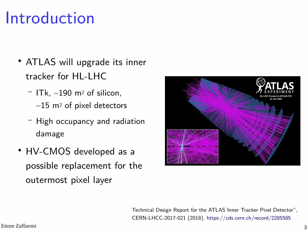
● ATLAS will upgrade its inner tracker for HL-LHC– ITk, ~190 m2 of silicon,
~15 m2 of pixel detectors– High occupancy and radiation
damage● HV-CMOS developed as a
possible replacement for the outermost pixel layer
Technical Design Report for the ATLAS Inner Tracker Pixel Detector”,CERN-LHCC-2017-021 (2018). https://cds.cern.ch/record/2285585
Ettore Zaffaroni 4
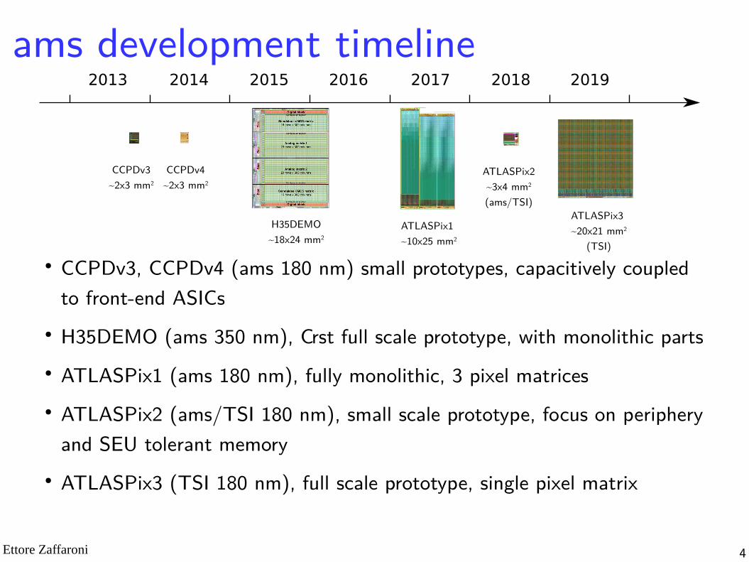
ams development timeline
● CCPDv3, CCPDv4 (ams 180 nm) small prototypes, capacitively coupled to front-end ASICs
● H35DEMO (ams 350 nm), first full scale prototype, with monolithic parts● ATLASPix1 (ams 180 nm), fully monolithic, 3 pixel matrices● ATLASPix2 (ams/TSI 180 nm), small scale prototype, focus on periphery
and SEU tolerant memory ● ATLASPix3 (TSI 180 nm), full scale prototype, single pixel matrix
2013 2014 2015 2016 2017 2018 2019
CCPDv3~2x3 mm2
CCPDv4~2x3 mm2
H35DEMO~18x24 mm2
ATLASPix1~10x25 mm2
ATLASPix2~3x4 mm2
(ams/TSI)ATLASPix3~20x21 mm2
(TSI)
Ettore Zaffaroni 5
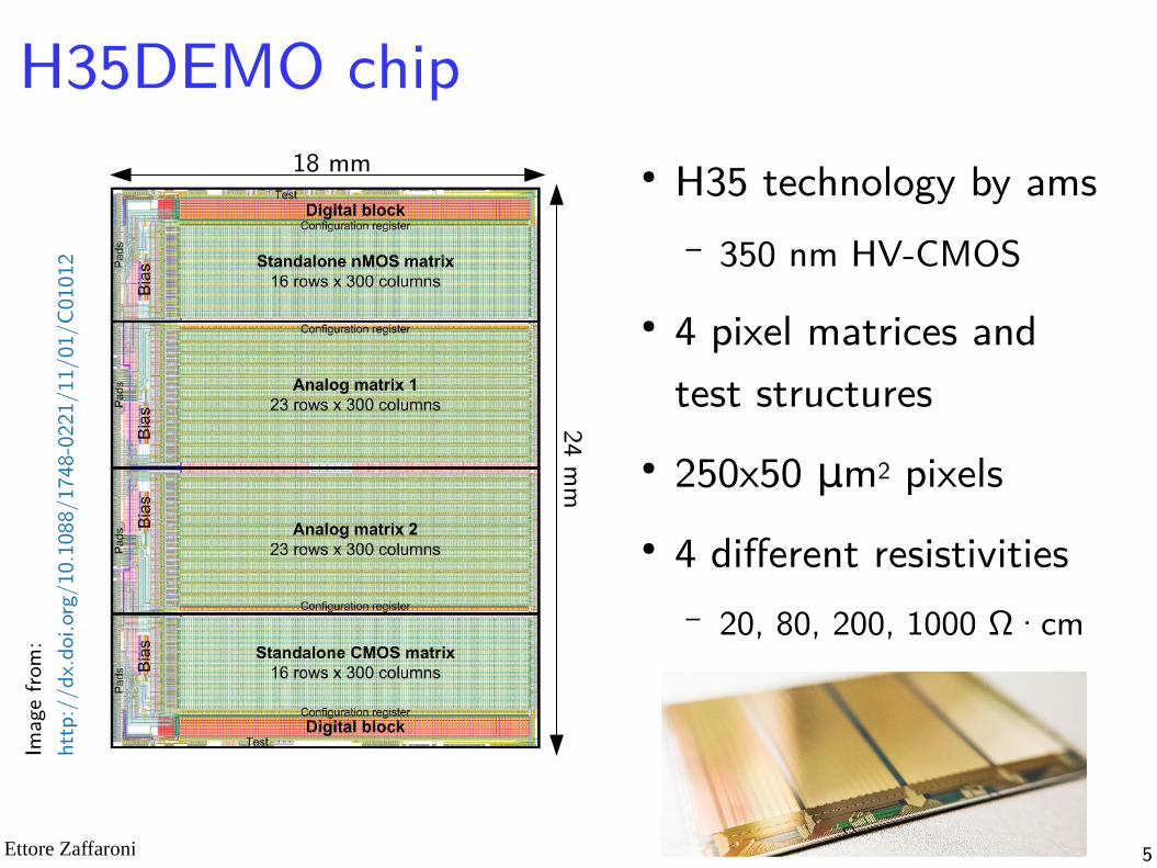
H35DEMO chip● H35 technology by ams
– 350 nm HV-CMOS● 4 pixel matrices and
test structures● 250x50 mμm 2 pixels● 4 different resistivities
– 20, 80, 200, 1000 Ω·cmcm
Imag
e fro
m:
http
://d
x.do
i.org
/10.
1088
/174
8-02
21/1
1/01
/C01
012
18 mm
24 mm
Ettore Zaffaroni 6
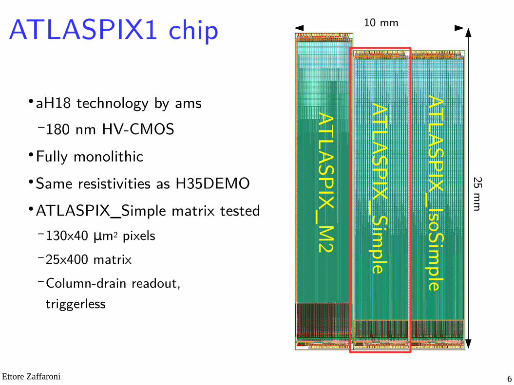
ATLASPIX1 chip
●aH18 technology by ams–180 nm HV-CMOS
●Fully monolithic●Same resistivities as H35DEMO●ATLASPIX_Simple matrix tested
–130x40 mμm 2 pixels–25x400 matrix–Column-drain readout,triggerless
ATL ASP IX_ IsoS impl e
ATL ASP IX_ Simp le
ATL ASP IX_ M2
10 mm25 m
m

Ettore Zaffaroni 7
Transient Current Technique
Ettore Zaffaroni 8
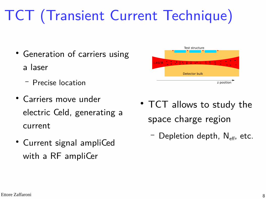
TCT (Transient Current Technique)
● Generation of carriers using a laser– Precise location
● Carriers move under electric field, generating a current
● Current signal amplified with a RF amplifier
● TCT allows to study the space charge region– Depletion depth, Neff, etc.
LASER + ++ + + + + + +
++
+
++
+
-- - - - - - - - - - - - -
- +
-
Detector bulk
Test structure
z position
Ettore Zaffaroni 9
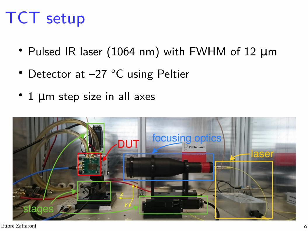
TCT setup● Pulsed IR laser (1064 nm) with FWHM of 12 μmm● Detector at –27 °C using Peltier● 1 μmm step size in all axes
Ettore Zaffaroni 10
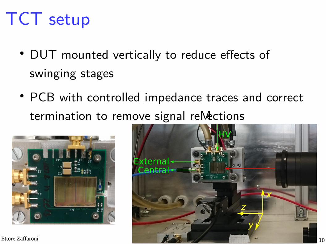
TCT setup● DUT mounted vertically to reduce effects of
swinging stages● PCB with controlled impedance traces and correct
termination to remove signal reflections
Ettore Zaffaroni 11
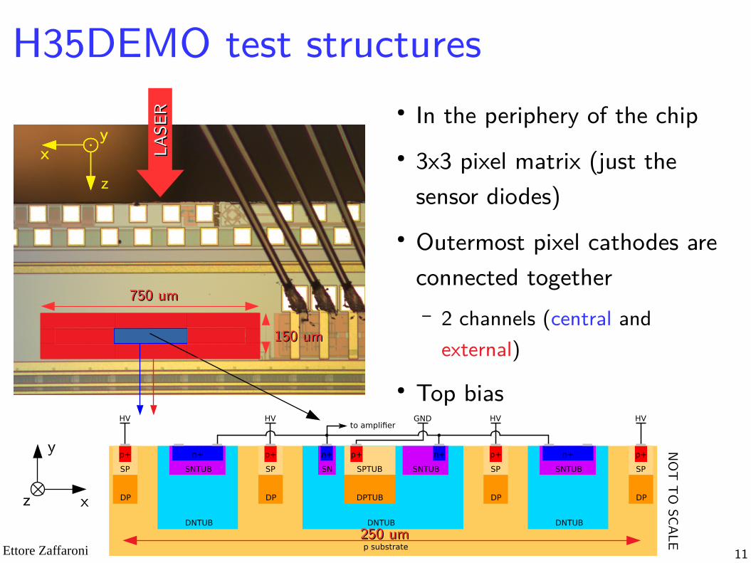
H35DEMO test structures● In the periphery of the chip● 3x3 pixel matrix (just the
sensor diodes)● Outermost pixel cathodes are
connected together– 2 channels (central and
external)● Top bias
750 um750 um
150 um150 um
LASE
RLA
SER
n+
SNTUB
DNTUB
SN
n+
SNTUB
n+
DNTUB
p+
SP
DP
HV
p+
SP
DP
HV
p+
SP
DP
HV
p+
SP
DP
HV
n+
SNTUB
DNTUB
p substrate
to amplifier
p+
SPTUB
DPTUB
GND
NOT TO
SCALE250 um250 um
zx
yx
yx
y
x
y
z
Ettore Zaffaroni 12
Irradiation campaigns
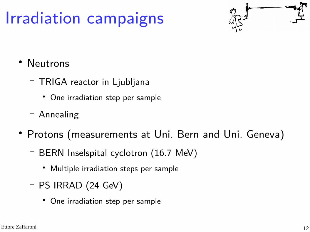
● Neutrons– TRIGA reactor in Ljubljana
● One irradiation step per sample
– Annealing● Protons (measurements at Uni. Bern and Uni. Geneva)
– BERN Inselspital cyclotron (16.7 MeV)● Multiple irradiation steps per sample
– PS IRRAD (24 GeV)● One irradiation step per sample
Ettore Zaffaroni 13
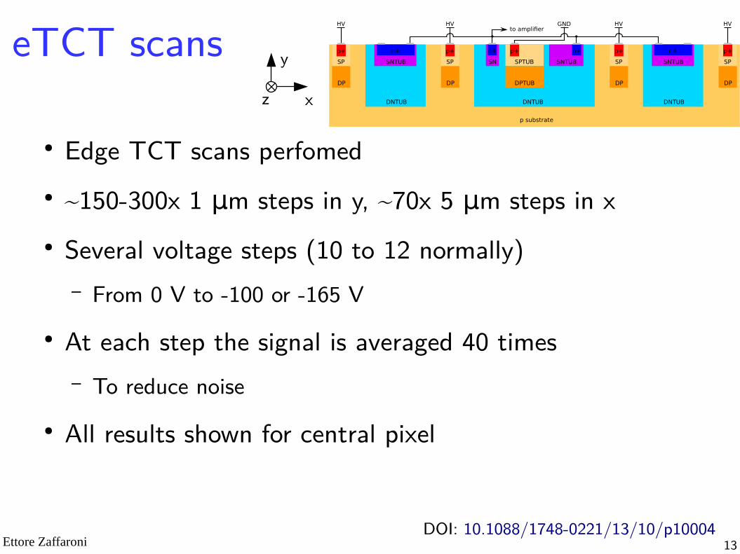
eTCT scans
● Edge TCT scans perfomed● ~150-300x 1 m steps in y, ~70x 5 μm m steps in xμm
● Several voltage steps (10 to 12 normally)– From 0 V to -100 or -165 V
● At each step the signal is averaged 40 times– To reduce noise
● All results shown for central pixel
n+
SNTUB
DNTUB
SN
n+
SNTUB
n+
DNTUB
p+
SP
DP
HV
p+
SP
DP
HV
p+
SP
DP
HV
p+
SP
DP
HV
n+
SNTUB
DNTUB
p substrate
to amplifier
p+
SPTUB
DPTUB
GND
x
y
z
DOI: 10.1088/1748-0221/13/10/p10004
Ettore Zaffaroni 14
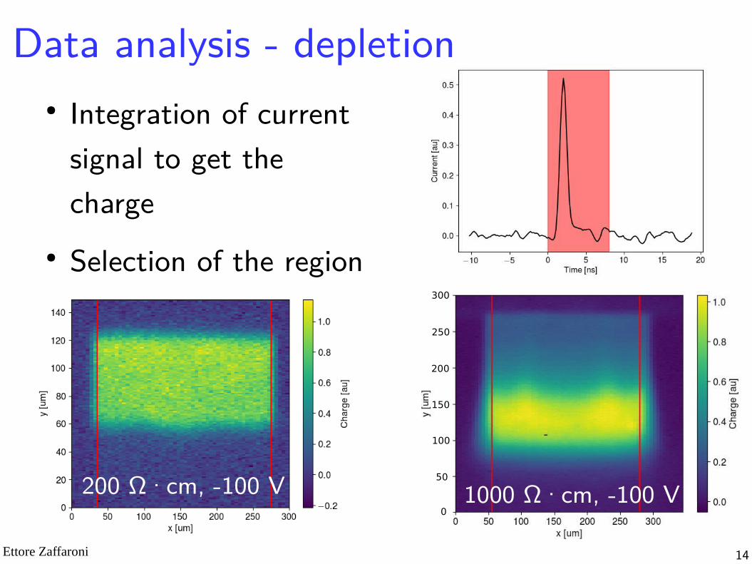
Data analysis - depletion● Integration of current
signal to get the charge
● Selection of the region of interest
1000 Ω·cmcm, -100 V200 Ω·cmcm, -100 V
250
200
150
100
50
0
300
Ettore Zaffaroni 15
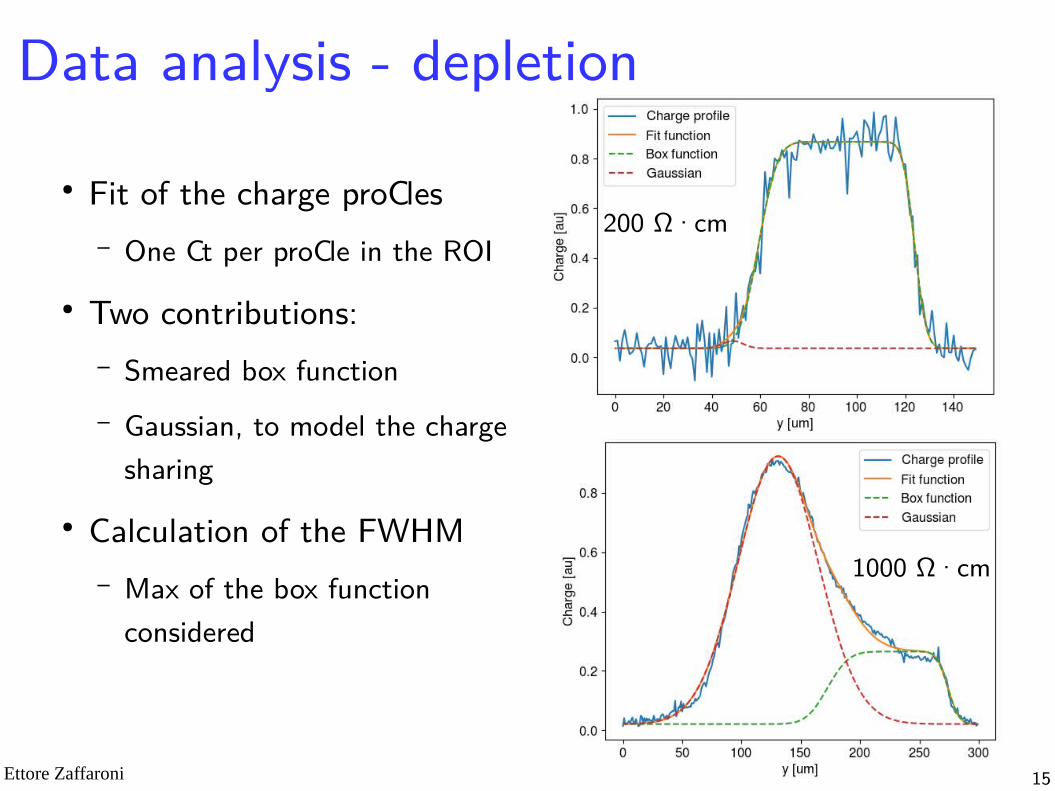
Data analysis - depletion
● Fit of the charge profiles– One fit per profile in the ROI
● Two contributions:– Smeared box function– Gaussian, to model the charge
sharing● Calculation of the FWHM
– Max of the box function considered
200 Ω·cmcm
1000 Ω·cmcm
Ettore Zaffaroni 16
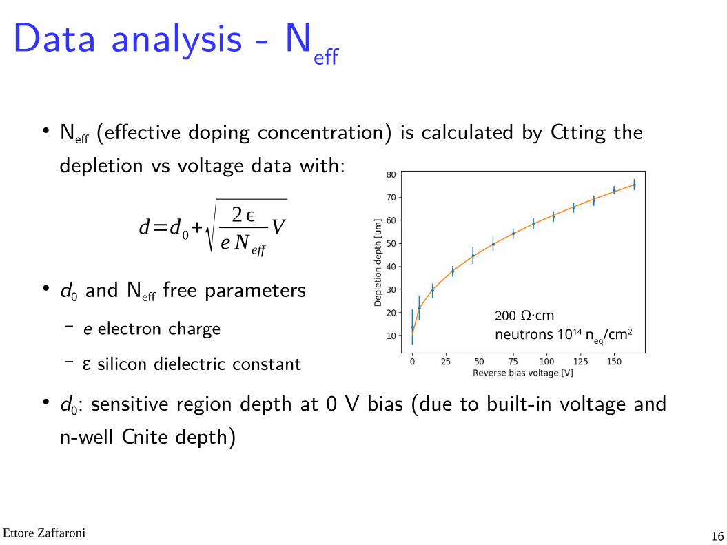
Data analysis - Neff
● Neff (effective doping concentration) is calculated by fitting the depletion vs voltage data with:
● d0 and Neff free parameters– e electron charge– ε silicon dielectric constant
● d0: sensitive region depth at 0 V bias (due to built-in voltage and n-well finite depth)
d=d0+√2ϵ
e N eff
V
200 Ω·cmcmneutrons 1014 neq/cm2
Ettore Zaffaroni 17
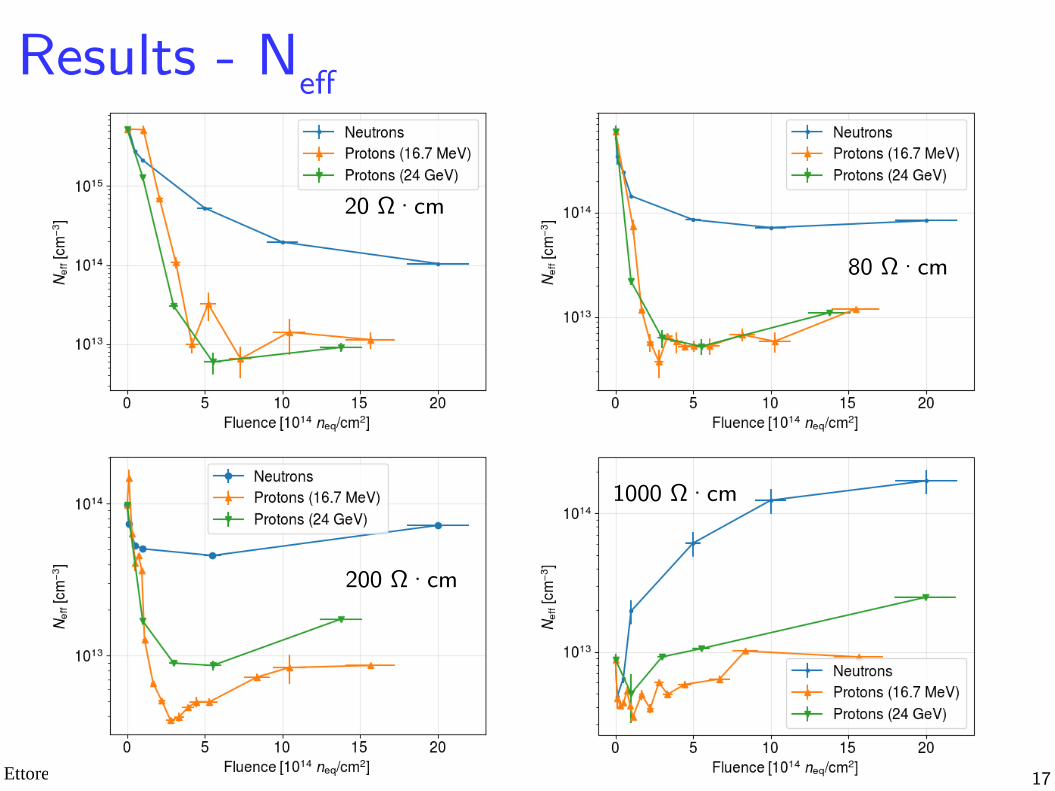
Results - Neff
20 Ω·cmcm
80 Ω·cmcm
200 Ω·cmcm
1000 Ω·cmcm
Ettore Zaffaroni 18
Results - Neff
● Acceptor removal at lower fluences (decrease of Neff)● Significant differences between protons and neutrons and
between resistivities● Initial increase of Neff at very low fluences
(<1e14 neq/cm2, protons) for the 200 Ω·cmcm sample– Effect competing with acceptor removal?– Not observed in 1000 Ω·cmcm, data not available for 20 and
80 Ω·cmcm
Ettore Zaffaroni 19
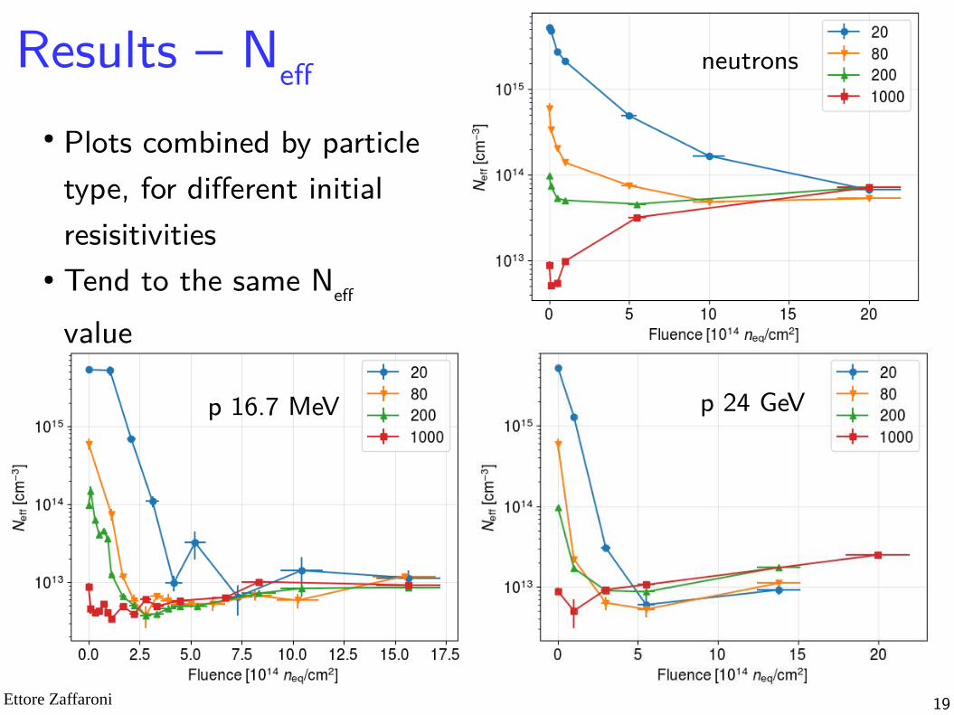
Results – Neff neutrons
p 16.7 MeV p 24 GeV
● Plots combined by particle type, for different initial resisitivities
● Tend to the same Neff value
Ettore Zaffaroni 20
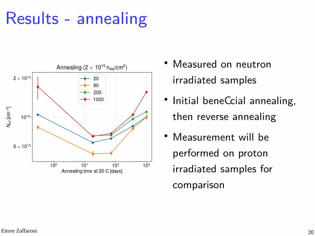
Results - annealing
● Measured on neutron irradiated samples
● Initial beneficial annealing, then reverse annealing
● Measurement will be performed on proton irradiated samples for comparison
Ettore Zaffaroni 21
Testbeams
Ettore Zaffaroni 22
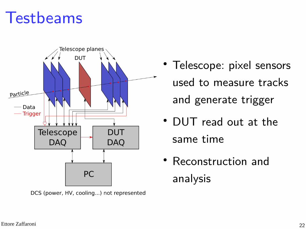
Testbeams
● Telescope: pixel sensors used to measure tracks and generate trigger
● DUT read out at the same time
● Reconstruction and analysis
Ettore Zaffaroni 23
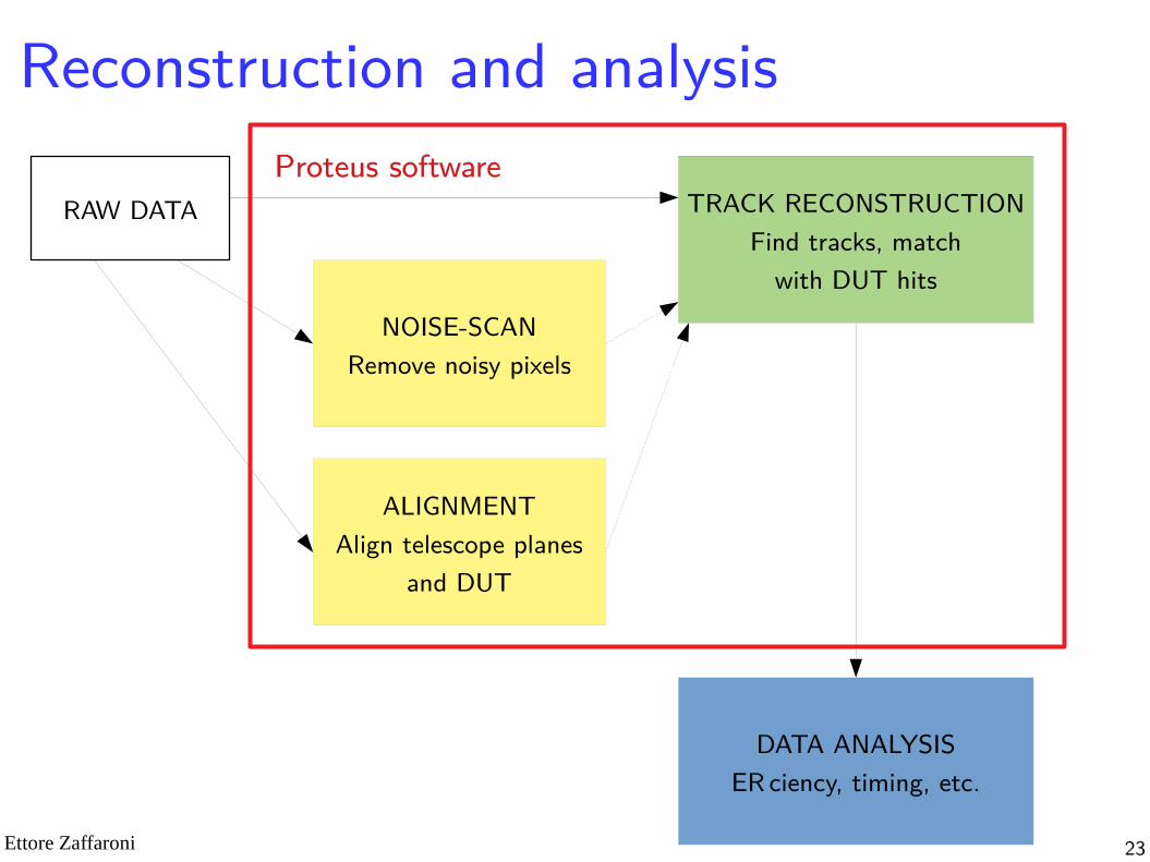
Reconstruction and analysis
RAW DATA
NOISE-SCANRemove noisy pixels
ALIGNMENTAlign telescope planes
and DUT
TRACK RECONSTRUCTIONFind tracks, match
with DUT hits
DATA ANALYSISEfficiency, timing, etc.
Proteus software
Ettore Zaffaroni 24
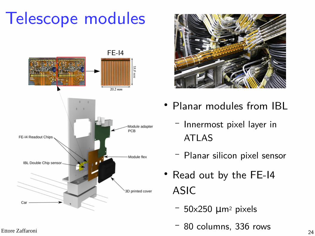
Telescope modules
● Planar modules from IBL– Innermost pixel layer in
ATLAS– Planar silicon pixel sensor
● Read out by the FE-I4 ASIC– 50x250 μmm2 pixels– 80 columns, 336 rows
FE-I4
Ettore Zaffaroni 25
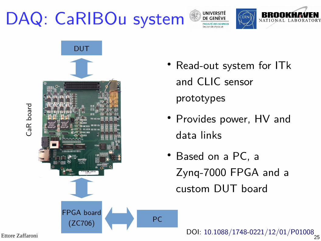
DAQ: CaRIBOu system
● Read-out system for ITk and CLIC sensor prototypes
● Provides power, HV and data links
● Based on a PC, a Zynq-7000 FPGA and a custom DUT board
FPGA board(ZC706)
DUT
PC
CaR
boar
d
DOI: 10.1088/1748-0221/12/01/P01008
Ettore Zaffaroni 26
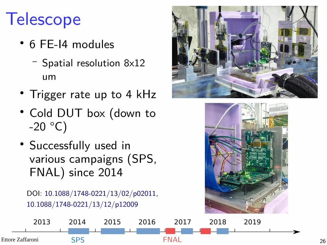
Telescope● 6 FE-I4 modules
– Spatial resolution 8x12 um
● Trigger rate up to 4 kHz● Cold DUT box (down to
-20 °C)● Successfully used in
various campaigns (SPS, FNAL) since 2014
2013 2014 2015 2016 2017 2018 2019
SPS FNAL
DOI: 10.1088/1748-0221/13/02/p02011, 10.1088/1748-0221/13/12/p12009
Ettore Zaffaroni 27
Measurement campaign
● Data acquisition at CERN SPS (06-10/2018)● Simple matrix of ATLASPIX1● Bias voltage and threshold scans● Different irradiations
– Protons (while operating the sensor)– Neutrons
Ettore Zaffaroni 28
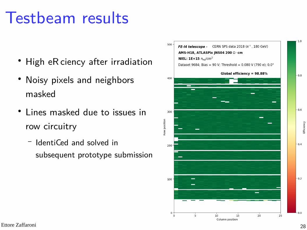
Testbeam results
● High efficiency after irradiation● Noisy pixels and neighbors
masked● Lines masked due to issues in
row circuitry– Identified and solved in
subsequent prototype submission
Ettore Zaffaroni 29
Testbeam results
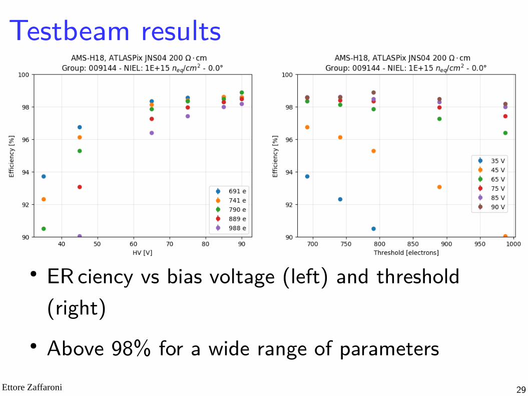
● Efficiency vs bias voltage (left) and threshold (right)
● Above 98% for a wide range of parameters
Ettore Zaffaroni 30
Testbeam results
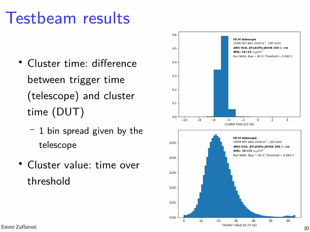
● Cluster time: difference between trigger time (telescope) and cluster time (DUT)– 1 bin spread given by the
telescope● Cluster value: time over
threshold
Ettore Zaffaroni 31
Comments
● Testbeams show excellent performance of ATLASPix1 before and after irradiation– Efficiency up to ~99% after 1015 neq/cm2
– Excellent timing performances● Identified issues in the circuitry, feedback
provided to the designers
Ettore Zaffaroni 32
Conclusions● TCT measurements
– Initial acceptor removal observed after proton and neutron irradiation– Beneficial and reverse annealing observed for neutrons– Significant differences between neutron and protons effects
● Testbeams – High, uniform efficiency over a large pixel matrix after irradiation– Very good timing performances
● Excellent results for fully monolithic pixel sensors!
Thank you!