Embed Size (px)
Citation preview
Current Applied Physics 4 (2004) 419–425
www.elsevier.com/locate/cap
Characterization of CdSexTe1�x sintered films
Monika Sharma a, Sushil Kumar b, L.M. Sharma a, T.P. Sharma c, M. Husain b,*
a Department of Chemistry, N.A.S. College, Meerut 250001, Indiab Department of Physics, Jamia Millia Islamia, New Delhi 110025, India
c Department of Physics, C.C.S. University, Meerut 250004, India
Received 7 January 2003; accepted 30 September 2003
Available online 21 November 2003
Abstract
CdSexTe1�x is a promising ternary material which has received considerable attention due to its applications in the fabrication oflarge area economic solar cell, semiconductor-metal Schottky barrier cell, etc. This material possesses various advantages, princi-
pally the high absorption coefficient, optimum band gap and chemical stability, which make it attractive for this kind of devices.
CdSexTe1�x films with variable concentration (x ¼ 0 to 1) have been deposited onto ultra clean glass substrates by screen printingand then sintered. The optical, electrical and structural properties of CdSexTe1�x alloys have been studied, which were foundapplicable in photovoltaics. The optical band gap of these films were determined by reflectance measurements in the wavelength
range of 700–880 nm. The modification of band gap of intermixed CdSexTe1�x system has been described and was found suitable forefficient absorption in the visible region of the spectrum. Schottky barrier height and ideality factor for Al/CdTe and Al/CdSe
junctions were determined by current–voltage characteristics. X-ray diffraction patterns of these films were reported. The films were
of polycrystalline texture over the whole range studied and exhibit predominant cubic zinc blende structure. Sintering is very simple
and viable compared to other costly methods. It is a technique less time-consuming, of maximum material utility and less pollutant
and offers a suitable method for preparing films on large area substrates.
� 2003 Elsevier B.V. All rights reserved.
PACS: 78.20.Cl; 78.50.Ge; 78.66.)w; 78.66.HfKeywords: Sintering; Band gap; Barrier height; Crystal structure; Photovoltaic
1. Introduction
Pseudo-binaries of II–VI, IV–VI and III–V group
compounds are attracting a great deal of attention be-
cause of their potential abilities in a wide spectrum of
optoelectronic devices [1–7]. Polycrystalline semicon-ductor materials have come under increased scrutiny,
because of their potential use in cost reduction of devices
for photovoltaic applications [8–13]. The band struc-
tures, optical properties and crystal structures of both
CdSe and CdTe are very similar and therefore the sys-
tem CdSexTe1�x would not only result in the feasibilityof graded energy gap of a broad spectral sensitivity but
many more material characteristics would be altered andexcellently controlled by the system concentration x. The
* Corresponding author. Fax: +91-11-6830337.
E-mail address: [email protected] (M. Husain).
1567-1739/$ - see front matter � 2003 Elsevier B.V. All rights reserved.
doi:10.1016/j.cap.2003.10.002
optical band gap of this ternary alloy CdSexTe1�x can betuned from 1.45 to 1.70 eV by changing the relative
amounts of the chalcogenides in the alloy. CdTe in film
form is a very promising photovoltaic material due to its
near optimum energy gap of 1.45 eV. Currently CdTe-
based solar cells have achieved efficiencies greater than16%, in which CdTe absorber layer is prepared by close
space sublimation process [14]. One of the simplest
techniques for fabricating the polycrystalline films of
AIIBVI compounds is the sintering. Solid solutions of
CdSe–CdTe are one of the important materials for use
in optoelectronic devices [15,16]. These films find appli-
cation in electro-optic devices, photoelectrochemical
solar cells and solar control coatings. Solar control coat-ing refers to selective solar radiation filters applied on
architectural glazings of buildings situated in warm cli-
mates [17,18]. CdSexTe1�x films with x varying from 0 to1 exhibit good solar control properties for use in tropi-
cal climate [19–21]. It has attracted the attention of
420 M. Sharma et al. / Current Applied Physics 4 (2004) 419–425
workers because of wide tunability of band gap as wellas lattice parameter [22,23]. Study has been undertaken
to investigate the photoactive properties of CdSexTe1�xsintered films.
2. Experimental details
There are a variety of methods reported in the liter-
ature for the preparation of CdSe–CdTe pseudo-binary
thin films. Thermal evaporation of pre-reacted samples
in vacuum [24,25], co-evaporation of CdSe and CdTe
powders in required quantities [26,27], three sourceevaporation of the elements [28], electron beam evapo-
ration [29], laser-induced formation [30], flash evapo-
ration [31], chemical methods [32,33], spraying and
sintering suspended mixtures of CdSe and CdTe [34–37],
etc. are commonly used techniques for the synthesis of
CdSexTe1�x films.CdSexTe1�x films have been prepared by screen-
printing followed by sintering [38,39]. For the prepara-tion of the films of CdSexTe1�x (x ¼ 0:00, 0.25, 0.50,0.75, 1.00), all the three compounds (CdSe, CdTe and
CdCl2) were mixed properly according to the concen-
tration required and then added few drops of ethylene
glycol to form the paste. Cadmium chloride acts as an
adhesive and ethylene glycol as binder. The desired
materials were formed as
Weight of CdSe ¼ 191:36 � x gmWeight of CdTe ¼ 240:00 � ð1� xÞ gmWeight of CdCl2 �H2O ¼ 10% weight of
ðCdSeþ CdTeÞAs these weights are quite large, we can reduce them
in the same proportion. The paste thus formed wasscreen printed on glass substrate, which has been
cleaned by soap solution, embry powder, HCl and fi-
nally washed with distilled water. The samples thus
prepared were dried at 120 �C for 4 h in open air andthen heated at 400 �C for 15 min to remove the organicmaterial left. The reason of drying the samples at lower
temperature was to avoid the cracks in the samples.
After this the films were sintered at 550 �C for 10 min.The melting point of CdCl2 is 568 �C. However, theevaporation of CdCl2 starts above 400 �C. Cadmiumchloride is hygroscopic, so to get a stable sintered film,
organic material and cadmium chloride should not re-
main in the sample. Hence to get a stable sintered film,
the sintering temperature was maintained at 550 �C.
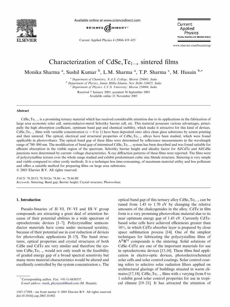
Fig. 1. Reflection spectra of CdSexTe1�x sintered films.
3. Characterization of samples and analysis
3.1. Optical characterization
The reflection spectra of CdSexTe1�x sintered filmswere recorded at room temperature in the wavelength
range of 700–880 nm using a Hitachi U3400 UV–VIS–NIR double beam spectrophotometer. The energy band
gaps of these films were determined by reflection spectra.
Almost all the II–VI compounds are direct band gap
semiconductors. According to the Tauc relation, the
absorption coefficient for direct band gap material is
given by [40]
ahm ¼ Aðhm � EgÞ1=2; ð1Þa may be written in terms of reflectance as [41]
2at ¼ ln½ðRmax � RminÞ=ðR� RminÞ�; ð2Þwhere R is the reflection for any intermediate energy
photons (hm), A is a constant which is different for dif-ferent transitions, Eg is the energy band gap and t is thethickness of the film.
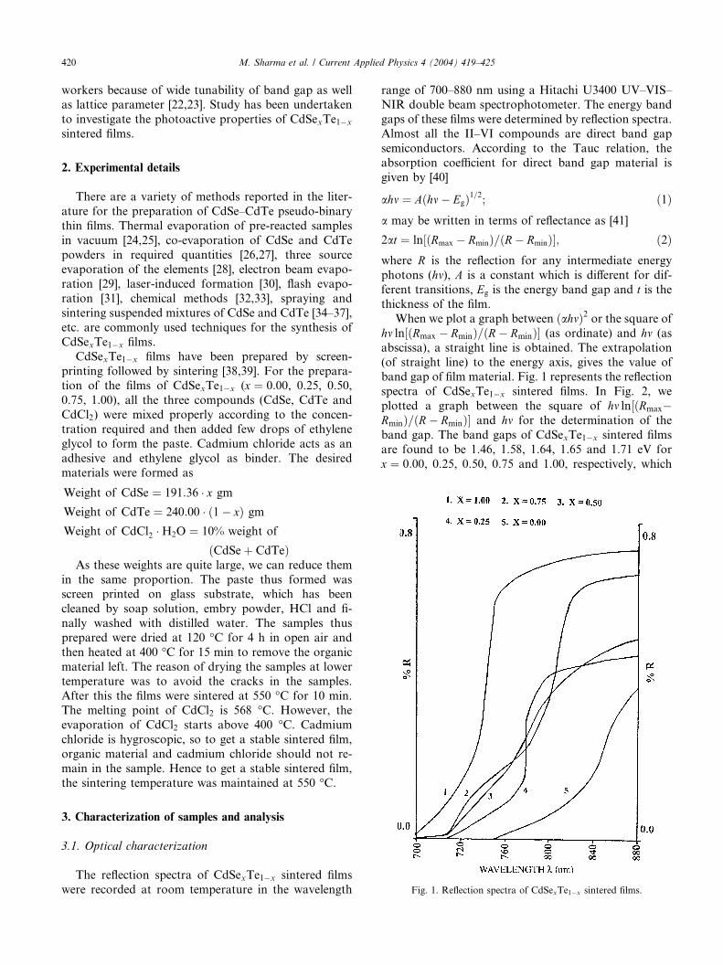
When we plot a graph between ðahmÞ2 or the square ofhm ln½ðRmax � RminÞ=ðR� RminÞ� (as ordinate) and hm (asabscissa), a straight line is obtained. The extrapolation
(of straight line) to the energy axis, gives the value ofband gap of film material. Fig. 1 represents the reflection
spectra of CdSexTe1�x sintered films. In Fig. 2, weplotted a graph between the square of hm ln½ðRmax�RminÞ=ðR� RminÞ� and hm for the determination of theband gap. The band gaps of CdSexTe1�x sintered filmsare found to be 1.46, 1.58, 1.64, 1.65 and 1.71 eV for
x ¼ 0:00, 0.25, 0.50, 0.75 and 1.00, respectively, which
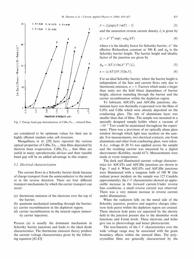
Fig. 2. Energy band gap determination of CdSexTe1�x sintered films.
M. Sharma et al. / Current Applied Physics 4 (2004) 419–425 421
are considered to be optimum values for their use in
highly efficient tandem solar cell structure.
Mangalhara et al. [29] have reported the various
optical properties of CdSexTe1�x thin films deposited byelectron bean evaporation. CdSexTe1�x thin films areuseful in many optoelectronic devices and their tunableband gap will be an added advantage in this respect.
3.2. Electrical characterization
The current flows in a Schottky barrier diode because
of charge transport from the semiconductor to the metal
or in the reverse direction. There are four different
transport mechanisms by which the carrier transport canoccur:
(a) thermionic emission of the electrons over the top of
the barrier;
(b) quantum mechanical tunneling through the barrier;
(c) carrier recombination in the depletion region;
(d) carrier recombination in the neutral region (minor-
ity carrier injection).
Process (a) is usually the dominant mechanism in
Schottky barrier junctions and leads to the ideal diode
characteristics. The thermionic emission theory predicts
the current–voltage characteristics given by the follow-
ing equation [42,43]:
J ¼ Js½expðeV =nkT Þ � 1� ð3Þand the saturation reverse current density Js is given by
Js ¼ AT 2 expð�e/B=kT Þ ð4Þ
where n is the ideality factor for Schottky barrier, A the
effective Richardson constant at 300 K and /B is theSchottky barrier height. The barrier height and idealityfactor of the junction are given by
/B ¼ ðkT=eÞ lnðAT 2=JsÞ; ð5Þ
n ¼ ðe=kT Þ½oV =oðln JÞ�: ð6Þ
For an ideal Schottky barrier, where the barrier height is
independent of the bias and current flows only due to
thermionic emission, n ¼ 1. Factors which make n largerthan unity are the field (bias) dependence of barrier
height, electron tunneling through the barrier and the
carrier recombination within the depletion region.
To fabricate Al/CdTe and Al/CdSe junctions, alu-
minium layer was thermally evaporated over the films of
CdTe and CdSe which were already deposited on the
conducting glass. The size of aluminium layer was
smaller than that of films. The sample was mounted in aspecially designed sample holder where a vacuum of
10�3 Torr could be maintained throughout the experi-ment. There was a provision of an optically plane glass
window through which light may incident on the sam-
ple. For measurements, two electrical contacts, one from
aluminium and other from conducting glass, were taken.
A d.c. voltage (0–20 V) was applied across the sample
and the resulting current was measured by a digitalelectrometer (Keithley, model 617). Measurements were
made at room temperature.
The dark and illuminated current–voltage character-
istics for Al/CdTe and Al/CdSe junctions are shown in
Figs. 3 and 4. When Al/CdTe and Al/CdSe junctions
were illuminated with a tungsten bulb of 100 W (the
radiant power incident on the sample was 127 Candela
approximately), the I–V characteristics showed an appre-ciable increase in the forward current.Under reverse
bias conditions, a small reverse current was observed.
There was a very minute increase in reverse current
under illumination.
When the radiation falls on the metal side of the
Schottky junction, positive and negative charges (elec-
tron–hole pairs) within the depletion region are created.
These electron–hole pairs are separated by the electricfield in the junction present due to the dissimilar work
functions and Fermi levels. These electrons and holes
give rise to photovoltage and hence photocurrent.
The non-linearity of the I–V characteristics over thewide voltage range may be associated with the grain
boundary effects within the sintered films. The poly-
crystalline films are generally characterized by the
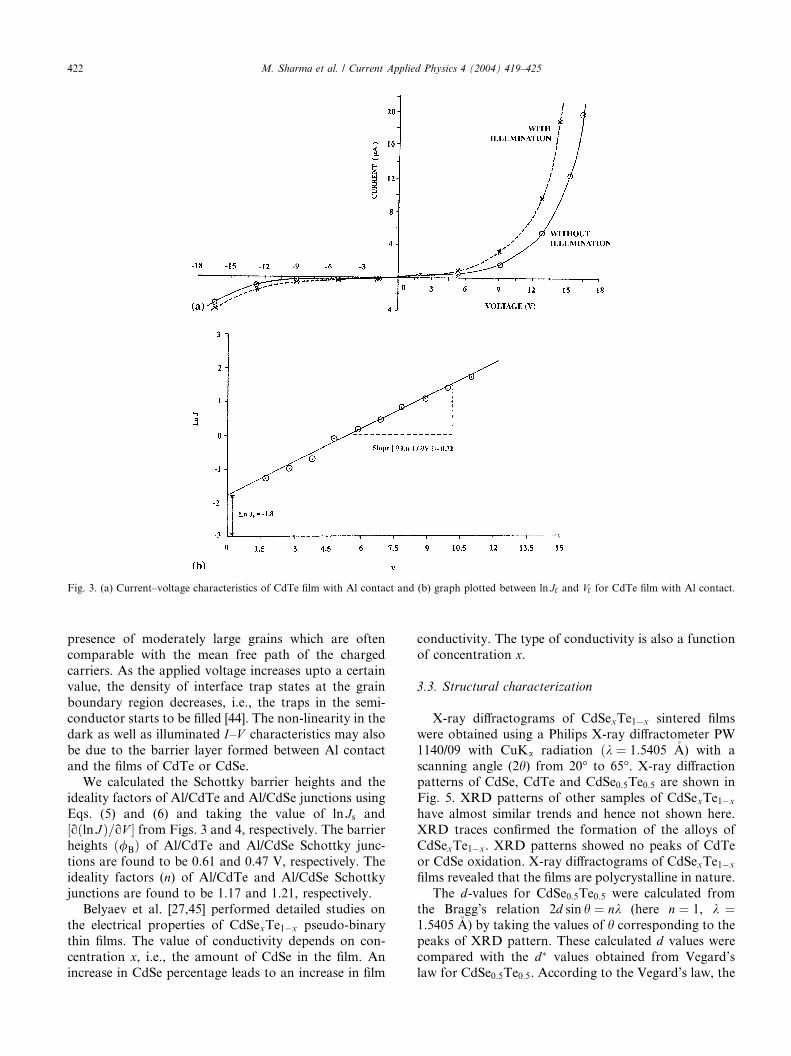
Fig. 3. (a) Current–voltage characteristics of CdTe film with Al contact and (b) graph plotted between ln Jf and Vf for CdTe film with Al contact.
422 M. Sharma et al. / Current Applied Physics 4 (2004) 419–425
presence of moderately large grains which are oftencomparable with the mean free path of the charged
carriers. As the applied voltage increases upto a certain
value, the density of interface trap states at the grain
boundary region decreases, i.e., the traps in the semi-
conductor starts to be filled [44]. The non-linearity in the
dark as well as illuminated I–V characteristics may alsobe due to the barrier layer formed between Al contact
and the films of CdTe or CdSe.We calculated the Schottky barrier heights and the
ideality factors of Al/CdTe and Al/CdSe junctions using
Eqs. (5) and (6) and taking the value of ln Js and½oðln JÞ=oV � from Figs. 3 and 4, respectively. The barrierheights ð/BÞ of Al/CdTe and Al/CdSe Schottky junc-tions are found to be 0.61 and 0.47 V, respectively. The
ideality factors (n) of Al/CdTe and Al/CdSe Schottkyjunctions are found to be 1.17 and 1.21, respectively.Belyaev et al. [27,45] performed detailed studies on
the electrical properties of CdSexTe1�x pseudo-binarythin films. The value of conductivity depends on con-
centration x, i.e., the amount of CdSe in the film. Anincrease in CdSe percentage leads to an increase in film
conductivity. The type of conductivity is also a functionof concentration x.
3.3. Structural characterization
X-ray diffractograms of CdSexTe1�x sintered filmswere obtained using a Philips X-ray diffractometer PW
1140/09 with CuKa radiation ðk ¼ 1:5405 �A) with ascanning angle (2h) from 20� to 65�. X-ray diffractionpatterns of CdSe, CdTe and CdSe0:5Te0:5 are shown in
Fig. 5. XRD patterns of other samples of CdSexTe1�xhave almost similar trends and hence not shown here.
XRD traces confirmed the formation of the alloys of
CdSexTe1�x. XRD patterns showed no peaks of CdTe
or CdSe oxidation. X-ray diffractograms of CdSexTe1�xfilms revealed that the films are polycrystalline in nature.
The d-values for CdSe0:5Te0:5 were calculated fromthe Bragg’s relation 2d sin h ¼ nk (here n ¼ 1, k ¼1:5405 �A) by taking the values of h corresponding to thepeaks of XRD pattern. These calculated d values werecompared with the d values obtained from Vegard’s
law for CdSe0:5Te0:5. According to the Vegard’s law, the
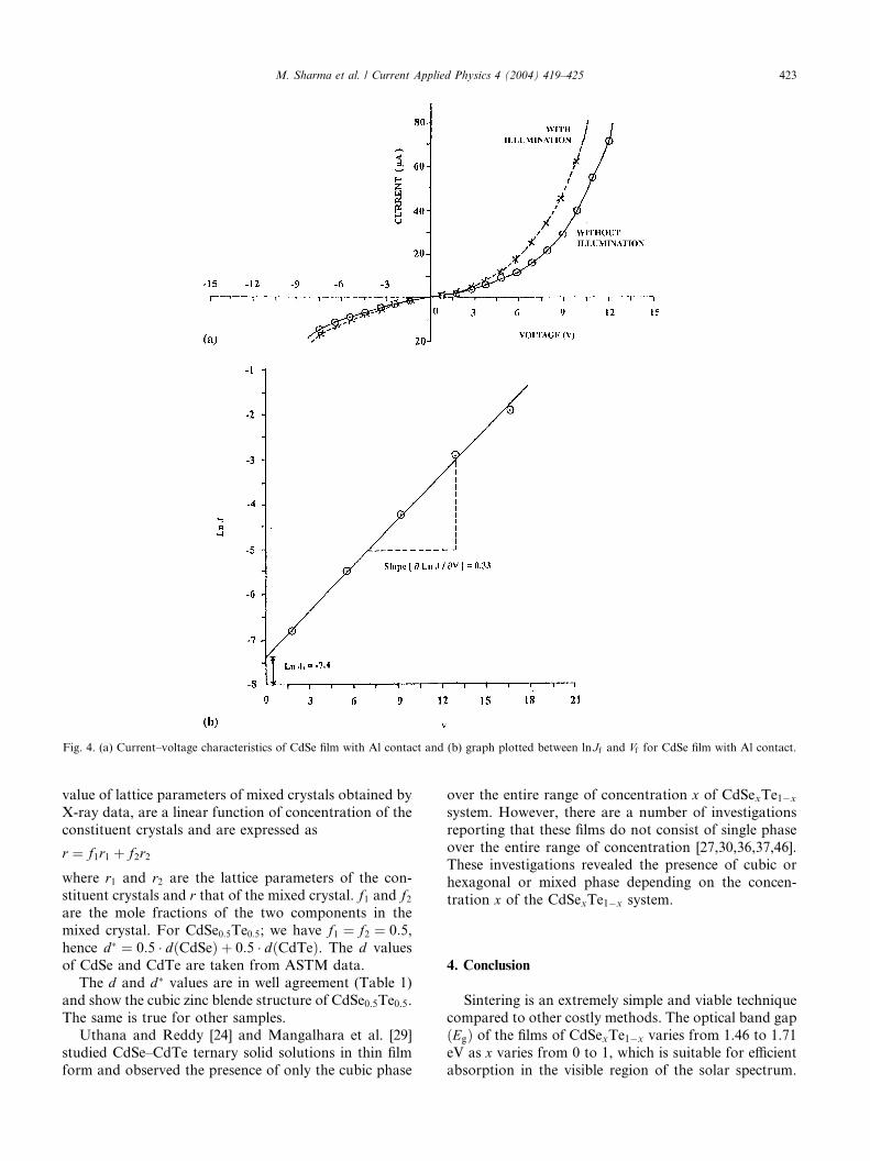
Fig. 4. (a) Current–voltage characteristics of CdSe film with Al contact and (b) graph plotted between ln Jf and Vf for CdSe film with Al contact.
M. Sharma et al. / Current Applied Physics 4 (2004) 419–425 423
value of lattice parameters of mixed crystals obtained by
X-ray data, are a linear function of concentration of the
constituent crystals and are expressed as
r ¼ f1r1 þ f2r2
where r1 and r2 are the lattice parameters of the con-stituent crystals and r that of the mixed crystal. f1 and f2are the mole fractions of the two components in the
mixed crystal. For CdSe0:5Te0:5; we have f1 ¼ f2 ¼ 0:5,hence d ¼ 0:5 � dðCdSeÞ þ 0:5 � dðCdTeÞ. The d valuesof CdSe and CdTe are taken from ASTM data.
The d and d values are in well agreement (Table 1)and show the cubic zinc blende structure of CdSe0:5Te0:5.
The same is true for other samples.Uthana and Reddy [24] and Mangalhara et al. [29]
studied CdSe–CdTe ternary solid solutions in thin film
form and observed the presence of only the cubic phase
over the entire range of concentration x of CdSexTe1�xsystem. However, there are a number of investigations
reporting that these films do not consist of single phase
over the entire range of concentration [27,30,36,37,46].These investigations revealed the presence of cubic or
hexagonal or mixed phase depending on the concen-
tration x of the CdSexTe1�x system.
4. Conclusion
Sintering is an extremely simple and viable techniquecompared to other costly methods. The optical band gap
ðEgÞ of the films of CdSexTe1�x varies from 1.46 to 1.71eV as x varies from 0 to 1, which is suitable for efficientabsorption in the visible region of the solar spectrum.
Fig. 5. X-ray diffraction patterns of CdSe, CdTe and CdSe0:5Te0:5 films
sintered at 550 �C for 10 min.
Table 1
Structural parameters of CdSe0:5Te0:5 sintered film
2h (degree) sin h d ¼ k=2 sin h(�A)
d (�A) Plane
(hkl)
24.50 0.2122 3.6298 3.6300 0 0 2
33.85 0.2911 2.6460 2.6445 1 0 2
40.42 0.3455 2.2290 2.2230 1 1 0
49.05 0.4151 1.8556 1.8595 2 0 1
62.40 0.5180 1.4870 1.4800 2 1 0
d values calculated from XRD pattern.
d values obtained from Vegard’s law.Sample: CdSe0:5Te0:5, sintering temperature¼ 550 �C.Wavelength: 1.5450 �A, sintering time¼ 10 min.
424 M. Sharma et al. / Current Applied Physics 4 (2004) 419–425
The barrier heights ð/BÞ of Al/CdTe and Al/CdSe
Schottky junctions are found to be 0.61 and 0.47 V,
respectively. The ideality factors ðnÞ of Al/CdTe and Al/CdSe Schottky junctions are found to be 1.17 and 1.21,respectively. CdSexTe1�x films prepared by sintering
technique are found to be polycrystalline in nature and
having cubic zinc blende structure.
References
[1] N.C. Sharma, D.K. Pandaya, H.K. Sehgal, K.L. Sharma, Thin
Solid Films 59 (1979) 157.
[2] L.P. Deshmukh, K.M. Garadkar, D.S. Sitrave, Mater. Chem.
Phys. 55 (1998) 30.
[3] L.P. Deshmukh, B.M. More, S.G. Holikatti, Bull. Mater. Sci. 17
(1994) 455.
[4] A.S. Nasibov, Y.V. Korostelin, L.G. Suslina, D.L. Fedorov, L.S.
Markov, Solid State Commun. 71 (1989) 867.
[5] A. Burger, M. Roth, J. Cryst. Growth 70 (1984) 386.
[6] P. Gupta, B. Maity, S. Chaudhuri, A.K. Pal, Thin Solid Films 260
(1995) 75.
[7] A.A. Bassam, A.W. Brinkman, G.J. Russell, J. Woods, J. Cryst.
Growth 86 (1988) 667.
[8] B. Ray, II–IV Compounds, Pergamon Press, Oxford, 1969.
[9] A.A. Bassam, The Arabian J. Sci. Eng. 15 (2B) (1990).
[10] A.A. Bassam, Solar Energy Mater. Solar Cells 57 (1999) 323.
[11] K.C. Sharma, J.C. Garg, J. Appl. Phys. 27 (1988) 1556.
[12] R.P. Sharma, Indian J. Pure Appl. Phys. 35 (7) (1997) 424.
[13] K.C. Sharma, R.P. Sharma, J.C. Garg, Jpn. J. Appl. Phys. 31
(1992) 742.
[14] J. Britt, C. Ferekides, Appl. Phys. Lett. 62 (1993) 2851.
[15] G. Hodes, D. Cohen, J. Manassen, M. David, J. Electrochem.
Soc. 127 (1980) 2252.
[16] G. Hodes, Nature (London) 285 (1980) 29.
[17] C.M. Lampert, Solar Energy Mater. 6 (1981) 1.
[18] I. Ritchie, C.K. Wilfred Jr., Proc. Soc. Photo-Opt. Instrum. Eng.
823 (1987) 2.
[19] P.J. Sebastian, V. Sivaramakrishnan, J. Phys. D 23 (1990) 1114.
[20] P.J. Sebastian, V. Sivaramakrishnan, Thin Solid Films 202 (1991)
1.
[21] P.J. Sebastian, V. Sivaramakrishnan, Solar Energy Mater. Solar
Cells 27 (1992) 321.
[22] B.M. Basol, V.K. Kapur, M.L. Perris, J. Appl. Phys. 66 (1989)
1816.
[23] T.I. Chu, S.S. Chu, C. Perikides, J. Britt, J. Appl. Phys. 71 (1992)
5635.
[24] S. Uthanna, P.J. Reddy, Solid State Commun. 45 (1983) 979.
[25] P.J. Sebastian, V. Sivaramakrishnan, Phys. Rev. B 42 (1990) 3057.
[26] M.A. Russak, J. Vac. Sci. Technol. A 3 (1985) 433.
[27] A.P. Belyaev, I.P. Kalinkin, Thin Solid Films 158 (1988) 25.
[28] M.A. Russak, C. Creter, J. Electrochem. Soc. 121 (1984) 556.
[29] J.P. Mangalhara, R. Thangaraj, O.P. Agnihotri, Solar Energy
Mater. 19 (1989) 157.
M. Sharma et al. / Current Applied Physics 4 (2004) 419–425 425
[30] L. Baufay, D. Dispa, A. Pigeolet, L.D. Laude, J. Cryst. Growth 59
(1982) 143.
[31] T.H. Weng, J. Electrochem. Soc. 117 (1970) 725.
[32] M.T. Gutierrez, J. Ortega, Solar Energy Mater. 20 (1990) 387.
[33] G. Hodes, J. Manasen, S. Neagu, D. Cahen, Y. Mirovsky, Thin
Solid Films 90 (1982) 433.
[34] I.B. Ermolovich, A.M. Pavelets, L.N. Khanat, Thin Solid Films
143 (1986) 225.
[35] I.D. Budyonnaya, A.M. Pavelets, L.N. Khanat, V.E. Badan, Thin
Solid Films 138 (1986) 163.
[36] I.B. Shevchenko, Yu.V. Nikolskii, E.M. Smirnova, V.R. Dar-
ashkevich, Yu.E. Sutyron, Inorg. Mater. 10 (1974) 184.
[37] M.I. Izakson, N.Ya. Karasik, L.M. Prokator, D.A. Sakseev, G.A.
Fedorova, I.N. Yakimenko, Inorg. Mater. 15 (1979) 178.
[38] V. Kumar, T.P. Sharma, J. Opt. Mater. 10 (1998) 253.
[39] S. Kumar, S.K. Sharma, T.P. Sharma, M. Husain, J. Phys. Chem.
Solids 61 (2000) 1809.
[40] J. Tauc, in: J. Tauc (Ed.), Amorphous and Liquid Semiconduc-
tors, Plenum, New York, 1974, p. 159.
[41] V. Kumar, S.K. Sharma, T.P. Sharma, V. Singh, J. Opt. Mater. 12
(1999) 115.
[42] S.M. Sze, Physics of Semiconductor Devices, Wiley Eastern, New
Delhi, 1979.
[43] B.L. Sharma (Ed.), Metal Semiconductor Schottky Barrier
Junctions and Their Applications, Plenum, New York, 1984.
[44] C. Crevecoueur, Phys. Lett. AA33 (1) (1970) 25.
[45] A.P. Belyaev, I.P. Kalinkin, V.A. Sanitarov, Sov. Phys. Semicond.
18 (1984) 1234.
[46] J. Steininger, A.J. Strauss, J. Cryst. Growth 13–14 (1972)
657.