Embed Size (px)
Citation preview

Wright State University Wright State University
CORE Scholar CORE Scholar
Browse all Theses and Dissertations Theses and Dissertations
2010
Characterization and Design of a Completely Parameterizable Characterization and Design of a Completely Parameterizable
VHDL Digital Single Sideband Modulator Circuit for Quick VHDL Digital Single Sideband Modulator Circuit for Quick
Implementation in FPGA or ASIC Electronic Warfare Platforms Implementation in FPGA or ASIC Electronic Warfare Platforms
Harold Scott Axtell Wright State University
Follow this and additional works at: https://corescholar.libraries.wright.edu/etd_all
Part of the Electrical and Computer Engineering Commons
Repository Citation Repository Citation Axtell, Harold Scott, "Characterization and Design of a Completely Parameterizable VHDL Digital Single Sideband Modulator Circuit for Quick Implementation in FPGA or ASIC Electronic Warfare Platforms" (2010). Browse all Theses and Dissertations. 386. https://corescholar.libraries.wright.edu/etd_all/386
This Thesis is brought to you for free and open access by the Theses and Dissertations at CORE Scholar. It has been accepted for inclusion in Browse all Theses and Dissertations by an authorized administrator of CORE Scholar. For more information, please contact [email protected].

CHARACTERIZATION AND DESIGN OF A COMPLETELY PARAMATERIZABLE
VHDL DIGITAL SINGLE SIDEBAND MODULATOR CIRCUIT FOR QUICK
IMPLEMENTATION IN FPGA OR ASIC ELECTRONIC WARFARE PLATFORMS
A thesis submitted in partial fulfillment
of the requirements for the degree of
Master of Science in Engineering
By
HAROLD SCOTT AXTELL
B.S., University of Akron, 2002
2010
Wright State University

WRIGHT STATE UNIVERSITY
SCHOOL OF GRADUATE STUDIES
June 14, 2010
I HEREBY RECOMMEND THAT THE THESIS PREPARED
UNDER MY SUPERVISION BY Harold Scott Axtell ENTITLED
Characterization and Design of a Completely Parameterizable VHDL
Digital Single Sideband Modulator Circuit for Quick Implementation
in FPGA or ASIC Electronic Warfare Platforms BE ACCEPTED IN
PARTIAL FULFILLMENT OF THE REQUIREMENTS FOR THE
DEGREE OF Master of Science in Engineering.
J.M. Emmert, Ph.D.
Thesis Director
Kefu Xue, Ph.D.
Department Chair
Committee on
Final Examination
J.M. Emmert, Ph.D.
Saiyu Ren, Ph.D.
Raymond Siferd, Ph.D.
John A. Bantle, Ph.D.
Interim Dean
of Graduate Studies

iii
ABSTRACT
Axtell, Harold Scott. M.S.E., Department of Electrical Engineering, Wright State
University, 2010. Characterization and Design of a Completely Parameterizable VHDL
Digital Single Sideband Modulator Circuit for Quick Implementation in FPGA or ASIC
Electronic Warfare Platforms.
In this work we present the design and characterization of a parameterizable Digital
Single Sideband Modulator (DSSM) circuit for use with a Digital Radio Frequency
Memory (DRFM) or other signal processing circuits. Field Programmable Gate Arrays
(FPGAs) can be used as a prototyping platform for quickly verifying and hardware
testing a digital circuit or system. FPGAs can also be used as an implementation
platform for a digital circuit or system. A main advantage of FPGAs over that of an
Application Specific Integrated Circuit (ASIC) is that it can be quickly (and often
dynamically) reprogrammed; whereas an ASIC can take months to fabricate.
Currently there is limited capability to quickly and easily generate backend digital signal
processing systems for electronic warfare (EW) applications for implementation on an
FPGA or an ASIC platform. It is advantageous (especially for dynamically
reprogramming FPGAs) for backend EW processing to have parameterizable hardware
description language (HDL) code to assist in quickly implementing digital processing
capabilities for EW systems. The purpose of this thesis work is to provide just such a
capability. We present a completely generic VHDL digital single sideband modulator
(DSSM) based on a parameterizable Hilbert Transform (HT). We characterize and test
the code so that the user can quickly implement a system to meet their expectations. The
entire system is described in VHDL to provide an inexpensive, long term, portable, and
parameterizable solution which allows for rapid design and redesign of DSSM circuits.
This design is technology portable so it will be viable now and in the future for rapid
prototyping, demonstration, and implementation. So as technology changes this code
transitions with it. The DSSM via HT rapidly delivers digital circuits for FPGA or ASIC
radar or other EW applications.
iv
TABLE OF CONTENTS
PAGE
I. INTRODUCTION .......................................................................................................1
Modulation ................................................................................................................................................. 2 The Hilbert Transform ................................................................................................................................ 9 Carrier Wave Generation .......................................................................................................................... 12 VHDL ....................................................................................................................................................... 13
II. RELATED WORK ....................................................................................................15
III. DSSM IMPLEMENTATION ....................................................................................29
Hilbert Transform Hardware Implementation .......................................................................................... 30 Sine & Cosine Generation ........................................................................................................................ 31 Test Plan ................................................................................................................................................... 34
Hilbert Transform Testing ................................................................................................................... 35 DDS Testing ........................................................................................................................................ 40 Digital Single Sideband Modulator Testing ......................................................................................... 41
IV. RESULTS AND ANALYSIS ....................................................................................43
HT Parameterization Point Effects ........................................................................................................... 44 Direct Digital Synthesizer ........................................................................................................................ 48 DSSM Parameterization Point Effects ...................................................................................................... 50 Two tone input .......................................................................................................................................... 51 Input Frequency Sweep ............................................................................................................................ 52
V. CONCLUSION ..........................................................................................................56
Future Work.............................................................................................................................................. 56
APPENDIX A ....................................................................................................................58
VHDL Source Code.................................................................................................................................. 58 Hilbert Transform ................................................................................................................................ 58 Sine and Cosine Wave Generation ...................................................................................................... 62 Multiply and Adder Block ................................................................................................................... 67 Testbench ............................................................................................................................................. 68
REFERENCES ..................................................................................................................81

v
LIST OF FIGURES
Figure 1 – Modulator .......................................................................................................... 3
Figure 2 – Single Sideband modulation via phase-shift method ........................................ 8
Figure 3 – Filter method of SSB generation ..................................................................... 16
Figure 4 – Phase method of SSB generation .................................................................... 16
Figure 5 – Weaver's method for single-sideband generation ............................................ 17
Figure 6 – System of 12 Weaver modulators.................................................................... 18
Figure 7 – A 12 channel digital Weaver modulator .......................................................... 19
Figure 8 – Darlington’s Recursive & Nonrecursive cascade filters ................................. 20
Figure 9 – Darlington’s optimized Weaver based DSSB modulator ................................ 20
Figure 10 – Analog Multiplex Weaver modulator ............................................................ 21
Figure 11 – Output frequency spectrum of the multiplex Weaver modulator .................. 23
Figure 12 – Modified multiplex Weaver modulator ......................................................... 24
Figure 13 – SSB generation by method proposed by Gurcan et. all ................................. 25
Figure 14 – Discrete Hilbert Transform block diagram .................................................... 31
Figure 15 – DSSM Block Diagram ................................................................................... 34
Figure 16 – HT signal Amplitude and Phase Error........................................................... 47
Figure 17 – DSSM Signal to Quantization Noise ............................................................. 50
Figure 18 – DSSM SQNR Input Frequency Sweep, 4 Input & Coefficient bits .............. 53
Figure 19 – DSSM SQNR Input Frequency Sweep, 8 Input & Coefficient bits .............. 55

vi
LIST OF TABLES
Table 1 – Discrete Hilbert Transform Tap values ............................................................ 12
Table 2 – HT output results for mixed HT parameters ..................................................... 45
Table 3 – DDS Amplitude and Phase Error and Signal to Quantization Noise ................ 48
Table 4 – DSSM output results for mixed HT parameters ............................................... 49
Table 5 – Two Tone Input Test Results ............................................................................ 52
Table 6 – Truncated Hilbert Transform Coefficients for 4 bits ........................................ 54

vii
ACKNOWLEDGEMENTS
This thesis would not have been possible without the unending amount of support and
encouragement from my family. My parents have instilled in me the values, morals, and
determination needed to accomplish any task in front of me. My siblings, their spouses,
and my in-laws have been a constant source of encouragement and a bright spark on dark
days. I owe my deepest gratitude to my wife and daughter, Heather and Isabella. Day
after day, they have been a driving force in my life and have sacrificed so that I can reach
this goal.
I am very grateful to my supervisor, Dr. Marty Emmert, for his encouragement, guidance
and support through this learning process. He has always made himself available to me
and pushed me to improve my abilities.
Special thanks go to my friend Vipul Patel for his persistent encouragement and lending
time to edit my work. I would like to give thanks to Dr. Ray Siferd and Dr. Saiyu Ren
for their guidance as part of my thesis committee. Also, thanks to the New Electronic
Warfare Specialists Through Advanced Research by Students (NEWSTARS) program
for sponsoring my research.
H. Scott Axtell

1
I. Introduction
As the war on terror continues there is a constant need for faster detection capabilities
with rapid deployment. To facilitate this increased need for speed the information
processing capabilities of most systems are implemented digitally on the backend of an
analog receiver system. In these systems the analog-to-digital converter (ADC)
component is a major bottleneck and lags behind development of other system parts due
to complexity. Because of this, most digital backend solutions are fixed and/or must be
used with proprietary software for configuration. This dramatically limits the use of the
high speed backend system making them only point solutions for each application. In
order to alleviate this costly process with limited use this work proposes a digital single
sideband modulator (DSSM) via parameterizable Hilbert transform (HT). This thesis
describes the design of an inexpensive, parameterizable, and technology portable DSSM
written in a simple language that will be viable now and in the future for rapid
prototyping, demonstration, and implementation in both field programmable gate array
(FPGA) and integrated circuit (IC) technology.
A radar topology has an analog/radio frequency (RF) front end with a digital backend.
The front end refers to all the analog, continuous time, components that make up the
radar from the antenna back to the ADC. This would include parts such as filters,
amplifiers, mixers, baluns, and power amplifiers. The back end refers to all the digital,
discrete time, components in the radar after the ADC. The front end through the antenna
captures the signal of interest, filters out unwanted frequencies, and amplifies the
information. The ADC then converts the analog signal into a digital one. The

2
transmission and reception of signals are much easier using RF techniques. The
processing of the signal is done much faster and easier digitally. The ADC is the link
between these sections.
The DSSM will be implemented after the ADC and its main function is to convert the
input signal to a desired frequency. The first step is to create a 90 degree phase shifted
copy of the input signal. These two signals, the original input and the 90 degree phase
shifted version, are then mixed with a pair of quadrature signals. And finally, the two
resultant signals are summed or subtracted to create the frequency converted signal. The
DSSM in this work is comprised of three major components: a quadrature modulator
known as the Hilbert transform, a direct digital frequency synthesizer (DDS), and a
summation block. The Hilbert transform creates the 90 degree phase shifted version of
the input signal. The original input signal is called the I, in phase, signal and the
modified signal is the Q, quadrature modulated, signal. The I and Q signals are then
mixed with a cosine and sine signal, respectively, generated by the DDS. These two
signals are then either added or subtracted to get the final output. The DSSM can
alleviate digital backend dependence on an analog front end through adaptability to any
ADC output allowing for independent design of the front and back ends.
Modulation
The DSSM is able to shift the frequency of a signal up or down the spectrum while
maintaining the input signal’s information through the use of modulation. Modulation is

3
an essential part of communication systems in order to easily transmit, receive, and
process signals. It involves two signals, the modulating signal containing the information
and a carrier signal, Figure 1 below. The modulator’s function is to impress the
modulating signal’s message upon the carrier. In this manner the resulting modulated
wave carries the message [1]. The carrier is chosen by the user based on the application
needs. Modulation occurs in a transmitter while the reverse process of demodulation is
carried out in the receiver to recover the message from the modulated signal. The
resulting modulated signal’s frequency is based on the input and carrier signal frequency.
If it’s higher than the input frequency it’s considered to be up converted or down
converted if it’s lower.
Figure 1 – Modulator
This ability to shift the message signal’s frequency is quite significant with many
applications. One everyday application deals with the common radio signal transmission.
If all of the radio stations transmitted at the same frequency then each station’s signal
would interfere with one another and the messages would be lost. To avoid this, each
station is assigned a specific frequency band and a tuner on the radio is used to select one.
The frequency from every radio station starts off as human speech or music over an
audible range of 300 to 3500 Hz [6]. A modulator is then used to shift the frequency up
to the radio stations assigned frequency band for transmission. At home your radio’s

4
tuner is used to select a specific frequency and the demodulator shifts it to a common
intermediate frequency (IF). By using a common IF frequency this allows the use of a
single tuned IF amplifier for signals from any radio station [8]. Without the use of a
modulator to bring signals down to a common frequency a separate set of tuned
components would be needed for every radio station. This would make radios physically
larger and heavier and more expensive because of the additional components needed.
Modulation also enables the ability to send multiple signals across the same medium,
such as phone lines. This process is called multiplexing and the two prevalent methods
are frequency division multiplexing (FDM) and time division multiplexing (TDM) [1].
Another reason for frequency translation is due to physical antenna requirements. For
efficient radiation of electromagnetic energy, the antenna must be longer than 1/10 of the
wavelength [6, 9]. The wavelength is a physical distance and can be found using
Equation 1 below. Lambda (λ) is the wavelength, c is the speed of light, and f is the
frequency of interest.
f
c
s
mc 8100.3
(1)
Without modulation this would mean your home radio antenna would have to be at least
100 km long to receive the 300 Hz signal. This is not physically practical so commercial
AM and FM broadcasting frequencies are shifted/modulated to 535 – 1605 kHz and 88-
108 MHz, respectively. The lowest frequency of 535 kHz requires an antenna length of
56.02 meters. For a broadcasting company it’s easy enough to build a tower to this
optimum length. For the average listener at home a 56 meter antenna isn’t practical but
5
not necessary. Broadcasting stations increase their output power to make up for the non-
ideal antenna length of your radio.
The frequency shift is easily described by the frequency shifting property of the Fourier
Transform. We can represent a time domain signal f(t) in the frequency domain by taking
the Fourier Transform of that signal F(ω)=F[f(t)]. We can also generate the time domain
representation from the frequency domain by taking the inverse Fourier Transform,
f(t)=F-1
[F(ω)]. The transform pairs and their associated equations are listed respectively
below in Equations 2 and 3 [6].
)()()( 1 FFtftfFF
)()( Ftf (2)
deFtf
dtetfF
tj
tj
)(2
1)(
)()(
(3)
These equations are very important in the study of signal analysis because they allow us
to move between the time and frequency domain. If we take the time domain function
f(t) and multiply it by tj
e 0 this is the same as a frequency shift by ω0, Equation 4 below.
)()(
)()()()(
0
0
)(
0
000
Fetf
FdtetfdteetfetfF
tj
tjtjtjtj
(4)
This can also be seen if we multiply the function f(t) by tj
e 0 in Equation (5) below.

6
)()(
)()()()(
0
0
)(
0
000
Fetf
FdtetfdteetfetfF
tj
tjtjtjtj
(5)
Frequency shifting in the time domain is accomplished by multiplying the function by a
sinusoid because tj
e 0 is not a real function that can be generated [6]. If we use cosω0t as
our sinusoidal signal and use Euler’s identity we get the following equation.
tjtjetfetfttf 00
2
1cos)( 0 (6)
From here we can substitute Equations 4 and 5 into Equation 6 and get the final form of
the frequency shift equation for the cosine function [6].
0002
1cos)( FFttf (7)
This equation shows that by multiplying a function in the time domain by a sinusoid
results in the generation of two signals, located at ω±ω0, with half the amplitude.
The frequency shift can also be seen in the time domain as a result of the trigonometric
product formula.
)cos()cos(2
1coscos yxyxyx (8)
In the equation above, we will let x represent the modulating signal carrying the speech or
music at frequency fm. The carrier signal is represented by cos(y) at frequency fc. If we
assume the input and carrier signals are pure tones, they can further be represented by

7
cos(2πfmt) and cos(2πfct) respectively [3]. Substituting into Equation 7 above results in a
form of modulation called double sideband suppressed carrier (DSB-SC) amplitude
modulation (AM) [8].
tfftfftftf mcmcmc )(2cos2
1)(2cos
2
1)2cos()2cos( (9)
The result of DSB-SC modulation is two signals, one down converted to the frequency fc-
fm and the other signal up converted to frequency fc+fm. The signal at fc-fm is called the
lower sideband (LSB) and at fc+fm is the upper sideband (USB) [6]. The upper and lower
sidebands are symmetrical about the carrier frequency so they both contain the entire
message signal which is a waste of bandwidth. Also note the amplitude of the original
signal is cut in half, denoted by the ½ on the right side of the equation. DSB-SC
modulation does shift the frequency but wastes bandwidth and transmission power [1].
Another form of modulation is single sideband (SSB) which eliminates one of the
sidebands saving bandwidth. Filtering can be used to achieve SSB modulation by
generating the DSB-SC signal and then using a bandpass filter to eliminate the upper or
lower sideband [8]. Another method is the phase shift method shown in Figure 2 which
was chosen for this thesis. The phase shift method uses two DSB-SC signals that are 90
degrees out of phase and a pair of quadrature carriers [7]. The DSB upper and lower
sidebands are phased such that they cancel out on one side and add on the other [1]. The
Hilbert transform is used to generate the phase shifted copy of the input signal and will be
discussed in more detail in the following section. This signal is referred to as the

8
quadrature (90 degree phase shifted) signal, or Q signal. The original input signal is
referred to as the in-phase signal, or I signal [7].
Figure 2 – Single Sideband modulation via phase-shift method
Looking at Figure 2, the input to the DSSM is split into the I and Q channel. The I
channel runs along the top portion directly into the modulator and the Q channel runs
through the bottom portion passing through the Hilbert transform before the modulator.
After the input signal passes through the modulator on the I channel it will be in the form
of Equation 9. Before modulation in the Q channel, the input signal passes through the
Hilbert Transform where its phase is shifted by 90 degrees and of the form sin(2πfmt).
This signal is then modulated with the carrier sin(2πfct), see Equation 10 below.
tfftfftftf mcmcmc )(2cos2
1)(2cos
2
1)2sin()2sin( (10)
Finally, the two signals from Equation 9 and 10 are either added or subtracted to get the
frequency shifted lower or upper sideband. In Equation 11 below, the I and Q channel
signals are subtracted to get the upper sideband signal.

9
)2sin()2sin()2cos()2cos( tftftftfQI mcmc
tfftfftfftff mcmcmcmc )(2cos2
1)(2cos
2
1)(2cos
2
1)(2cos
2
1
tff mc )(2cos (11)
In the equation above it can be seen that by subtracting these two modulated signals we
end with the upper sideband as noted by fc+fm. To get the lower sideband these two DSB-
SC signals would be added. Also note the absence of the ½ in the front of the final form
of Equation 11. All of the signal power and bandwidth is concentrated at this one
frequency point, fc+fm.
The Hilbert Transform
The Hilbert transform is a filter implemented through convolution whose main function is
to create a copy of the input signal that is 90 degrees out of phase while maintaining the
amplitude. It’s based on the signum function which is similar to a unit step function, but
with odd symmetry about the vertical axis. The signum function is defined below in
Equation 11 [1].
(11)
It has the following Fourier Transform.

10
fjjtF
12sgn (12)
The transfer function can be written in terms of the signum function since a ±90 degree
phase shift is equivalent to multiplying by je j90 [1].
(13)
This indicates that all positive frequencies will have a -90 phase shift and a +90 degree
phase shift for negative ones. To find the corresponding impulse response we use the
duality theorem with the Fourier Transform of the signum function as follows,
)sgn()sgn(1
1sgn
fftj
F
fjtF
(14)
The impulse response, h(t), can then be found by adding the phase shift, ±j, to the result
in Equation 14 and taking the Inverse Fourier Transform.
tth
ttj
jfjF
1)(
1sgn1
(15)
The Hilbert Transform system response can now be defined as a convolution of the
modified signum impulse, Equation 15, and an input x(t) as seen in Equation 16.
ttxtx
1)()(ˆ (16)

11
For the actual implementation of the discrete Hilbert Transform, Oppenheim [7] gives the
following equation for the filter tap coefficient values. It is zero outside of the specified
interval, 0≤n≤M, making it a finite impulse response (FIR) type filter where n is the
current sample number, M is the number of delays, and nd is the number of delays divided
by two [7]. A filter tap is on either side of each delay so the total number of taps will be
M+1.
(17)
The following table lists the Hilbert Transform coefficient tap values for a 4 through 12
order (M) filter. The filter order is listed across the top of the table with the tap number
on the left side.
Number of Delays (M)
4 5 6 7 8 9 10 11 12
0 0.0000 -0.2546 0.0000 -0.1819 0.0000 -0.1415 0.0000 -0.1157 0.0000
1 -0.6366 0.0000 -0.3183 0.0000 -0.2122 0.0000 -0.1592 0.0000 -0.1273
2 0.0000 -1.2732 0.0000 -0.4244 0.0000 -0.2546 0.0000 -0.1819 0.0000
3 0.6366 0.0000 0.0000 0.0000 -0.6366 0.0000 -0.3183 0.0000 -0.2122
4 0.0000 0.4244 0.0000 1.2732 0.0000 -1.2732 0.0000 -0.4244 0.0000
5 0.0000 0.3183 0.0000 0.6366 0.0000 0.0000 0.0000 -0.6366
6 0.0000 0.2546 0.0000 0.4244 0.0000 1.2732 0.0000
7 0.0000 0.2122 0.0000 0.3183 0.0000 0.6366
8 0.0000 0.1819 0.0000 0.2546 0.0000
9 0.0000 0.1592 0.0000 0.2122
10 0.0000 0.1415 0.0000
11 0.0000 0.1273
12 0.0000
Ta
p C
oeff
icie
nt
Nu
mb
er

12
Table 1 – Discrete Hilbert Transform Tap values
Looking at the values in the table above, the HT filter will be a Type III or IV FIR filter
because none of the sets of taps are symmetrical. If M is even it will be a Type III, or IV
if it’s odd. By choosing an even number for M, making it a type III, gives an advantage
in that the even indexed samples of the impulse response are always zero [7]. This means
that we only need to compute half of the coefficient values during instantiation. More
importantly, during continuous operation we only need to compute half of the
multiplications originally needed per cycle. When M is even and twice divisible by 2, M
= 4, 8, 12, the numbers have a point symmetry with the maximum value around the
center as 0.6366. We could also take advantage of this by calculating half the values and
mirror them with the opposite sign to complete the coefficient values saving some storage
space.
Carrier Wave Generation
In order for modulation to occur the input signal needs to be mixed, or modulated, with a
carrier signal. It can be generated through an external source, such as a signal generator,
or created within the overall system through the use of a sine-wave synthesizer. The
three methods mainly used today for frequency synthesis are phase-locked loops (PLLs),
direct analog (DA), and direct digital synthesis (DDS) [4].

13
The PLL method is the most widely used today due to its low cost and relatively simple
design. It is a non-linear feedback loop whose output frequency is dependant on the input
control voltage. DA synthesis design is more complicated and thus more expensive than
PLL design but offers excellent signal to noise ratio and fast switching speeds. At the
center of both of these techniques is a feedback amplifier that is adjusted to get the
desired range of frequencies making them analog based methods. The DDS is purely a
digital technique where the sine wave samples are generated, instead sampling a sine
wave to get the needed samples [4]. The DDS method was chosen for this
implementation to enable an all digital SSB implementation without the need for external
signal generators.
VHDL
Very high-speed integrated circuit Hardware Description Language (VHDL) code allows
for several different points of customization to this application based on changing ADC
needs and desired accuracy. It enables the user to integrate the DSSM with almost any
ADC through the ability to choose the input frequency, power level, number of input bits,
and a second input signal can be added. Its accuracy and/or physical space required can
be modified by adjusting the number of filter taps, coefficient bit size, and windowing
function to make these tradeoffs. VHDL also allows for quick re-design based on
changing requirements.

14
One of the great benefits of using VHDL is it ensures the use of this code for many years
to come without cost. VHDL is an open source language and requires no special tools or
packages to run it. It is not technology dependent so as FPGA and ASIC technology
advances this will still be applicable. Because of this, many years from now this code
will be able to be used and modified to fit current application needs without any cost or
risk of becoming obsolete. There will be no need to worry about future investments in
software upgrades, additional packages for expanded capabilities, or finding a select few
with the knowledge of how to use it.

15
II. Related Work
The following section illustrates earlier designs and the beginnings of digital single
sideband (SSB) generation. Each presents the information in a unique way and some
build on prior work. I have used this information as a baseline for my work, to get a
better understanding of the challenges involved, and to create a standard of expectations
for the conclusions of my work.
A basic method used for single sideband generation is the Weaver method. Donald
Weaver presented this method in 1956 in the Proceedings of the Institute of Radio
Engineers. It is based on two widely known techniques of the time and combines them
into a single more efficient form. These include filters with sharp cutoff frequencies or
wideband 90 degree phase difference networks which his does not use.
The filter method uses a series of balanced modulators and filters to create and detect the
single sideband signal, Figure 3. The input signal is combined in the balanced modulator
with the carrier frequency producing the two sidebands. The balanced modulator
removes the carrier frequency and the following filter passes the intended sideband while
rejecting the other. When the desired frequency location of the SSB is high compared
with the original location of the input signal, it becomes very difficult to obtain filters that
will pass one sideband and reject the other [11]. In order to relax the filter requirement
additional pairs of balanced modulators and filters can be added in series.

16
Figure 3 – Filter method of SSB generation
The phasing method uses a 90 degree phasing network to create two signals from the
input that are equal in amplitude but whose phase differ by 90 degrees, Figure 4. Using
the same method, the translating frequency is also split into two 90 degree components.
Each of the outputs of the phasing network is applied to a balanced modulator with one of
the translating frequencies. Each balanced modulator will suppress the carrier while
passing the two sidebands. The signals are then summed, cancelling out one of the
sidebands and leaving a single sideband. However, the phases and amplitudes must be
very tightly controlled because they will dictate the amount of suppression of the
unwanted sideband.
Figure 4 – Phase method of SSB generation
It is possible to achieve 60 to 80 dB suppression using the filter method and up to 40 dB
using the phasing method [11]. This is based on maintaining low modulation in the linear

17
amplifiers used in the filter method and tight control of the amplitudes and phases in the
phasing method.
Weaver’s method uses both filtering and balanced modulators but does not require a strict
cutoff filter or wideband phase difference networks. His method, Figure 5, splits the
input into two channels that feed into a parallel set of balanced modulators. The signals
then pass through low pass filters and another set of balanced modulators. Lastly, the
balanced modulator outputs are summed for the final output. The carrier frequency of the
first balanced modulator is the center frequency of the input signal and of the desired
sideband signal for the second one [11].
Figure 5 – Weaver's method for single-sideband generation
After the input passes through the first modulator the signal is down converted and
centered at zero. The frequency range the signal originally occupied is now unoccupied
providing a wide transition region for the low pass filter. The final pair of modulators is
centered at the intended frequency of the final single sideband output. The two signals
are then combined in the final summing circuit to produce the desired single sideband
signal.

18
In two tone tests the undesired signal was more than 30 dB below the desired signal.
Additional advantages include a bilateral design so it can be used for modulation &
demodulation, mostly passive components for greater reliability, and lack of critical
and/or expensive designed elements [11].
In 1970 Sidney Darlington built upon Weaver’s design and looked at DSSB modulation
from a system standpoint comparing Hartley and Weaver modulators. His initial
calculations showed that using Hartley modulators would require fewer computations
than the Weaver method, but proposes a system of 12 Weaver modulators that would
yield an even greater computational reduction. This paper focuses on optimizing the
proposed Weaver system design by reducing the number of multiplications per second.
This implementation is intended for insertion into a larger analog system through the use
of analog-to-digital (ADC) converters on the input and digital-to-analog (DAC)
converters on the output, Figure 6. The proposed system of Weaver modulators is
designed to accept the 12 digitized inputs and form them into a single output.
Figure 6 – System of 12 Weaver modulators

19
He estimated that using a Hartley topology there would need to be 13x106 multiplications
per second and scratch pad storage of 192 words. In comparison, the Weaver topology in
Figure 7 below would take double the amount of multiplications per second. This
topology takes the Weaver method as is and sums the 24 outputs, yn(tn), to form a single
output, z(tn) [2].
Figure 7 – A 12 channel digital Weaver modulator
To increase the efficiency of the Weaver architecture for implementation in the 12
channel system Darlington splits the low-pass filter into two cascaded filters, Figure 8.
The first filter is a recursive filter designed for and outputs at 2fo samples per second. It
is more complex than the second filter with sharp cutoff frequencies, but requires fewer
multiplications per second. The second filter is a non-recursive filter designed for 16x2fo
to reach the required number of output samples per second. This filter is less complex
with a longer cutoff period and eliminates extraneous frequencies due to the low
sampling rate of the first filter [2].

20
Figure 8 – Darlington’s Recursive & Nonrecursive cascade filters
The second step involves combining the 12 channel system output starting from the
nonrecursive filter. This includes the 24 nonrecursive filters, product modulators and the
summation that yields the digital system output. Through this optimization only every
16th
sample needs calculated, it’s periodic with a period of 32, and when the value is
calculated it only takes 76 multiplications. The final optimized system is shown below in
Figure 9.
Figure 9 – Darlington’s optimized Weaver based DSSB modulator
Darlington estimates the total multiplication rate to be less than 3.3x10⁶ multiplications
per second and scratch pad storage of 450 words. This is all at a cost of increased
complexity and additional scratch pad storage. Compared to the Hartley method, that’s a
savings of 9.7x10⁶ multiplications per second.

21
Another IEEE Transaction paper entitled, ‘Digital Single-Sideband Modulation,’ by
Singh, Renner, and Gupta built on Darlington’s work. The authors were able to cut the
number of modulators in half by implementing multiplexed modulators allowing 2
signals per modulator. This enabled them to decrease the computation time while
increasing the accuracy. In addition they also discussed and created a demodulation
system which required the design of a band-pass filter.
The evaluation started with the system Darlington proposed utilizing the Weaver
modulator, Figure 5. The input sampling frequency is 2fo, the low pass filter is split into
a recursive and nonrecursive filter in cascade, and the output sample rate is at 16x2fo
samples per second. The additional step taken was to multiplex the Weaver modulators
enabling them to halve the number needed from 12 to 6.
Figure 10 – Analog Multiplex Weaver modulator
The figure above is an analog version of the multiplex Weaver modulator. The following
equations show mathematically how two signals can be simultaneously modulated as
single sideband at two different carrier frequencies. The two signals in question,
)cos( 111 tE and )cos( 222 tE are multiplexed as the sum and difference of one
another at the input to yield the following equations.

22
)cos()cos( 2221111 tEtEe
)cos()cos( 2221112 tEtEe (18)
The inputs e1 & e2 then pass through the first set of modulators whose center frequency
matches the input signal frequencies.
tee oa cos2 11
tee ob sin2 21 (19)
The constant multiplier 2 in equations (19) is used for mathematical convenience. The
intermediate signals ea2 and eb2 are then found by substituting equations (18) into (19),
simplifying, and neglecting those terms with frequencies outside the passband of the low-
pass filter with cutoff frequency fo, become
2221112 coscos tEtEe ooa
2221112 sinsin tEtEe oob (20)
The modulating signals ea2 and eb2 are then combined with the carrier frequency
terms tccos and tcsin , respectively, to obtain 3ae and 3be . It is important to note that
the carrier frequencies are not the same.

23
222
222
111
111
3
cos2
cos2
cos2
cos2
tE
tE
tE
tE
e
ococ
ococa
and
222
222
111
111
3
cos2
cos2
cos2
cos2
tE
tE
tE
tE
e
ococ
ococb
(21)
Finally combining 3ae and 3be , the output becomes
222111 coscos tEtEe ococo (22)
The equation above shows that the multiplex modulator in Figure 10 will modulate one
signal as the lower sideband and the other as the upper sideband with modified carrier
frequencies oc and oc , respectively and illustrated below.
Figure 11 – Output frequency spectrum of the multiplex Weaver modulator
In order to properly sample the multiplexed signals the input sampling rate was increased
from Darlington’s 2fo to 4fo Hz. This change provides the improved accuracy by

24
reducing the number of interpolated samples from 16 to 8. Also, for an nth order filter
the number of additions is reduced by 8n and the multiplications by 64n which results in
a reduced computation time. Figure 12 below is the final digital multiplexed version of
an element of the single sideband system.
Figure 12 – Modified multiplex Weaver modulator
A Fortran simulation of a single multiplex Weaver modulator and demodulator was run
as proof of validity. Due to computational limitations at the time they were only able to
achieve an output sample rate of four times the input sample rate instead of 16 out of the
recursive filter. They were able to provide input and output simulation plots which were
delayed by 200 samples to allow for settling.
The most recent attempt found for digital single sideband modulation was in 1988. The
authors of a paper submitted to the IEEE International Symposium on Circuits and
Systems created a digital single sideband modulator (DSSM) which was again based on
the analog Weaver topology. The overall design is similar to the basic Weaver modulator

25
through down conversion to baseband and filtering to remove the unwanted sideband.
The authors then wanted to avoid the possibility of mismatch error in the design of the
local oscillators and mixers so they came up with a unique implementation that uses two
stages of interpolation to reach the desired output frequency and a multiplexer to combine
the I and Q channels to form the output.
The input signal is band limited by a band-pass filter and sampled at a frequency of fs1,
Figure 13. It is then split into the I and Q channel where a pair of quadrature mixers
move the signal of interest to baseband and a low-pass filtered to remove the unwanted
sideband. The first interpolation is carried out using a low-pass filter, taking the signal to
30 times higher than the bandwidth of the I and Q low pass filters. This step is necessary
to be able to increase the sampling rate to fs3 using a linear interpolator without
introducing spurious signals [5].
Figure 13 – SSB generation by method proposed by Gurcan et. all

26
The linear interpolator design used to increase the sampling frequency by a factor of 4N
is based on a tapped delay line filter. Its impulse response in the frequency domain lasts
for two bit periods (2/fs2) and is defined by the following equation [5].
2
2
2
2
2
2sin
s
s
f
f
f
f
(23)
The tap weights give a triangular shape and the delay line filter is fed at fs3 with signal
samples at fs2 followed by 4N-1 zeros [5]. It can then be shown that this interpolating
filter can be replaced by a pair of multipliers and an adder through the following
equations. At any given time there will be two samples, x1 and x2, separated by T=1/fs2
due to the filter impulse length of 2/fs2. The signal at the output of the filter will the be
21 bxaxy (24)
where a and b are the coefficients of the convolution filter at the nth and (n+4N)th taps.
Due to the triangular shape of the impulse response the coefficients a and b are
N
nb
N
na
41
4 (25)
then substituting a and b into the equation for y
N
xxnxbxaxy
4
)( 21221 (26)
Therefore to interpolate the sampling frequency fs2 by a factor of 4N, take the difference
of the two samples x1 and x2 at the sampling rate fs2 and divide the result by the

27
interpolation factor 4N. This result is then taken as an increment and accumulated to x2
at every instance n to produce the interpolated samples of the input signal at a new
sampling frequency fs3 = 4Nfs2. When a new sample is interpolated from fs2 to fs3 the
accumulator is reset to zero and it continuously increments at a rate of fs3 for 4N clock
periods [5]. Finally, when the I and Q signal samples are multiplied by the carrier at fs3
the output will be in the sequence I channel, Q channel, negative I channel, and negative
Q channel. This will allow the use of a multiplexer and two inverters in the place of a
multiplier.
A floating point simulation was conducted using Pascal/VS on an IBM 4381. The filters
used were Chebyshev type IIR filters of 5th
order and 0.1 dB passband ripple for the low-
pass and interpolation filters. Two simulations were completed with final carrier
frequencies of 40 kHz and 1.28 MHz. It was shown in power spectral density graphs for
both simulations that they were able to achieve 45 dB suppression of unwanted signals.
This demonstration proved they were able to design a completely digital SSB modulator
and achieve good results that can be suitable for integrated circuit technology.
A method is needed for digital single sideband generation that allows for quick design,
prototyping, and implementation in FPGA or integrated circuit technology with points of
customization and based on fixed point simulations. Until now, the available methods
offer single sideband generation based on unrealizable floating point simulations giving
approximate output characteristics. The method I am proposing has been coded in
VHDL which allows for custom design based on user input specifications and control of

28
several component parameters. This will allow for accuracy tradeoffs with the desired
output tolerances. Also, VHDL is an open language and can port to any FPGA or IC
fabrication technology which allows for automated design and layout in current and
future IC technologies.

29
III. DSSM Implementation
Through the initial paper study I found there was very little previous work done on digital
implementations of single sideband modulators. The majority of the papers found were
from the 1970s and an attempt in the late 1980s. All of the implementations were based
on the Weaver method which is a combination of two other methods, filtering and
phasing. The early work was mostly theoretical and only went as far as floating point
computer simulation. I was not able to find any work that was simulated with fixed point
values, could be quickly prototyped, compensated for the amplitude and phase error, or
allowed for tradeoffs based on user input.
This work was followed up with a MATLAB simulation to gain a better understanding of
the basic operation and layout of the single sideband modulator. The Hilbert Transfer
function in MATLAB simulation and VHDL synthesis proved to be the most time
consuming area of work. The MATLAB simulation is ideal with floating point values
and shows the validity of the design. But, floating point operation is not possible in
hardware and is a very limiting constraint. There were several decisions that had to be
made as to the number of bits of precision in order to maintain the accuracy of the Hilbert
Transform output.

30
Hilbert Transform Hardware Implementation
In section 0 the HT was reviewed in detail and Table 1 shows the coefficient values for a
4 through 12 order filter. When M, the filter order, is even and twice divisible by 2, M =
4, 8, 12, the tap values have a point symmetry with the maximum value around the center
at 0.6366. This implementation is preferable because the even tap values are zero
eliminating the computation time and hardware. Also, because of the point symmetry we
would only need to find the first half of the values and then put them in positive reverse
order for the other half. The problem with this choice is that all of the coefficient values
are less than one. In a fixed point binary two’s compliment implementation any number
less than one will be truncated to zero. In order to obtain hardware implementable values
the coefficients must be scaled to values greater than one. To do this a scaling factor
(SC) was introduced based on the number of coefficient bits (NC).
22
2NC
SC (27)
The scaling factor increases the HT coefficients to an implementable value. In effect we
move the radix point to the right giving a whole number that when truncated doesn’t
result in a value of zero.
With the implementation of a scaling value, SC, the radix point location must be tracked
so the bits chosen at the output correctly represent the intended result. The block diagram
below, Figure 14, represents the discrete HT implementation with the parameterizable
values highlighted. This implementation of the Hilbert Transform gives the user the

31
ability to manipulate the number of input bits (NI), coefficient bits (NC), filter taps (NT),
and window type (WIN).
Figure 14 – Discrete Hilbert Transform block diagram
From the figure above it can be seen that the in-phase, I, signal is the input signal delayed
by an amount equal to the order of the HT filter. The quadrature, Q, signal tap values are
taken on either side of the delay, z-1
, and are only at odd numbers because again the even
values are zero as discussed in section 0 above. Each input tap value, x[n], is multiplied
by the HT coefficient value, h[n], and the window tap value, w[t]. All of the values are
then summed for the final Q signal output.
Sine & Cosine Generation
The main function of the single sideband generator is to up or down convert the
frequency of the input signal. This conversion is accomplished with a modulator that
uses an internal or externally generated carrier signal from a signal generator and mixes it
with the input signal. If an input signal is modulated with a carrier without any additional

32
filtering or mixing a double sideband signal would be created and there would be three
distinct frequencies at the output: the carrier frequency, carrier plus the input frequency,
carrier minus the input frequency. This section discusses the internal generation of the
carrier frequency which makes modulation possible.
At the instantiation of the VHDL code the values of a quarter sine wave are generated
and stored in a ROM. The number of points representing the quarter wave is based on a
user defined value called the granularity (RG). Equation 28 below is used to calculate the
actual quarter wave values.
IRG
SC *180
*90
sin* (28)
A quarter of a wave, 90 degrees, is divided by the granularity, multiplied by π/180º to
convert to radians, and multiplied by the loop index (I) which increments from zero to
RG. The sine of this value is calculated and multiplied by SC, which is a scaling factory
based on the number of input bits in equation 29 below. It’s the largest possible two’s
compliment positive value. This ensures that the generated carrier signal reaches the full
peak positive value and is one away from the full negative value.
12 1NISC (29)
As the system clock toggles between zero and one a subsequent ROM address is accessed
and the value is output. To form the entire sine wave the ROM addresses are then
accessed in reverse order, negative forward, and then negative reverse. The cosine wave
is formed by accessing the values in a different order: reverse, negative forward, negative
reverse, and then forward. The frequency of the generated carrier signal is based on the
clock period and the granularity value. The ROM address values are output after the

33
system clock cycles so you must multiply the system clock period by the granularity.
This value then must be multiplied by four because there are 4 quarters per period.
Another point of user control to increase or decrease the signal generator frequency is
through the ‘step’ (R_STEP) value. The step indicates the number of ROM addresses to
skip for each clock cycle. With a step of one, each of the ROM addresses will be output.
With a step of 2, every other address will be output which reduces the number of points
and therefore increasing the frequency. Equation 28 below gives the final equation used
to calculate the carrier frequency for the modulation after the Hilbert transform in Figure
2. The carrier frequency is equal to the one divided by the clock period times the
granularity times four over the step value. Therefore if we have a clock period (Cp) of 25
ns, a granularity of two, and a step of one the carrier frequency will be 5 MHz. If
R_STEP is increased to 2 the frequency will be 10 MHz.
Step
yGranularitCp
f4*
*
1cossin, (30)
The purpose of the signal generator is to create carrier signals, sine and cosine, which are
used to mix with the information signals I and Q. This is a key step in the DSSM as it
will create two double sideband signals that when added or subtracted will remove the
carrier signal frequency and one of the sidebands leaving the up or down converted single
sideband signal.

34
Test Plan
The purpose of this test plan is to fully characterize the DSSM. The tests are intended to
cover the proper breadth and depth of the individual components and the system as a
whole. The DSSM is comprised of three major components; Hilbert Transform, DDS
sin/cos signal generator, and the Modulation & Summation block which is seen in Figure
15 below. The functionality of each component will be evaluated against a set input
followed by a complete system test. The Modulation and Summation component only
uses basic functionality, multiplying and adding, so there is no need to individually test
this component.
Figure 15 – DSSM Block Diagram
In order to fit specific applications or meet user requirements the Hilbert Transform and
carrier signal generator have 6 parameters that are user defined; 4 in the Hilbert
Transform and 2 in the signal generator. These parameters will be manipulated against a
set input while the component and system output is collected. The data will then be
evaluated to see how the component parameter manipulation affects the output. Another
set of tests will measure the signal to quantization nose by sweeping the input frequency

35
will holding the component parameters constant. The goal is to gather enough data to be
able to model the output based on the component parameters.
The DSSM code was designed and tested using Mentor Graphics ModelSim, PE Student
Edition 6.5d, advanced simulation and debugging software. A test bench was created to
inputs test signals into the DSSM and record the output. It can accept up to two input
signals at varying frequencies and power levels. This mixed with the six user defined
component parameters creates a very large test space with many different combinations.
In order to reduce the number of test cases specific values have been chosen for the input
and component parameters based on practical application.
There are 13 qualitative tests performed during each simulation. These tests will check
the precision and accuracy of the Hilbert Transform signal, the generated sine and cosine
signals, and of the final DSSM output. The calculated values are started after 500 clock
cycles to allow for settling. The following sections define the tests performed on the
Hilbert Transform and signal generator components and the DSSM.
Hilbert Transform Testing
This section outlines how the HT will be tested and the data collected to fully
characterize the digital implementation. The testing procedure will first be discussed
followed by the calculations performed on the collected data. These calculations will

36
give a clear understanding on how manipulation of the input parameters affects the
output.
The amplitude of the input is a ratio of the input power, in decibels (dB), based on the
predefined maximum amplitude Amax, equation 29 below. The input to the DSSM is
designed to accept two inputs for which the user can define the power, P1 and P2. For
ease of use the maximum amplitude of the input sinusoids is set to one, the unit circle.
Therefore, the amplitude of each sinusoid is a fraction of one based on its input power
relative to the other sinusoid’s input power. The greater the difference in input power the
greater the amplitude difference.
2max1
10
max
2
21
max
1
0.1
AAA
e
AA
dBPdBPP
A
d ynP
dyn
(29)
The tests are set-up to cycle through most of the component parameter combinations
based on the predetermined test values per input frequency combination. The first set of
tests will be performed using a single input frequency followed by a second round of
testing with the same component combinations but with two input tones. The majority of
the measured data calculations have been added to the VHDL code. These results will
then be graphed to show the actual performance of the DSSM and analyzed for a relation
between the input parameter combinations and output performance.

37
The following tests will be performed on the HT generated Q signal’s amplitude and
phase in relation to the I signal’s values:
1. Phase/Amplitude difference
2. Phase/Amplitude error
3. Average phase/amplitude difference
4. Average phase/amplitude error
5. Phase/Amplitude Standard deviation
These tests are intended to measure the accuracy of the manipulated input signal. The
overall objective of the Hilbert Transform is to modify the input signal’s phase by 90
degrees while maintaining the amplitude. For each discrete instance in time the scaled
amplitude value is calculated for both the I and Q channel by dividing the input number
by two raised to the number of input bits minus one, equation 30 below. These values are
then subtracted to find the difference between them. The amplitude of the HT created
quadrature, Q, signal should match the original input, I, signal. Therefore, the difference
between the scaled I and Q values should ideally be zero.
QvalueIvalueMag
QQvalue
IIvalue
NB
input
NB
input
12
12
(30)
To evaluate the phase difference between the scaled I and Q values they are converted
into degree measure. Ideally the phase difference should be 90 degrees.

38
coscos
2
360*arccoscos
2
360*arccoscos
QaIaAngle
QvalueQa
IvalueIa
(31)
To help quantify the degree of accuracy of the HT generated Q signal error calculations
are performed on the amplitude and phase. A general error calculation is made by
subtracting the measured value from the ideal value divided by the ideal value which is
then multiplied by 100 to get a percentage, equation 32 below.
100*90
90_
100*_
AngleErrPhase
Ivalue
QvalueIvalueErrAmp
(32)
Another measurement of interest is the average. The standard way to calculate the
average is to add up all the values and divide by the total number of values. But, in this
implementation the total number of values is too great to add together. Depending on the
implementation, the DSSM could run continuously creating an infinite number of values.
Therefore the average value must be calculated on a continuous basis based on available
values. The average value is initially calculated through the normal method, per the
equation below. The vales are summed and divided by the total number of values.
N
xX
i
N
i
N
1 (33)

39
If another value was added to the set we could modify the above equation to include the
next value and increase the divisor by one as in equation 34 below.
1
1
11
1
1
1
1
N
xXX
N
xX
i
N
iN
N
i
N
iN
(34)
It is then possible to solve equation 34 for the summation,
Ni
N
i
i
N
i
N
XNx
N
xX
*1
1
(35)
and substitute equation 35 into equation 34 to get the Running Average equation as
follows.
1
*
1
*
1
1
11
1
1
N
XNXX
N
xXX
XNx
NN
N
i
N
iN
N
Ni
N
i
(35)
The running average is the future value of the input plus the current number of values
times the current average all divided by the future number of values. The future value,
N+1, is actually the current value because the first number in the set is indexed as 0. The

40
first two values are averaged using index positions zero and one. The third value to be
added is at index position 2, but is the N+1 value. This running average equation is used
to find the average amplitude and phase difference and error between the I and Q signal.
Another calculation performed is the standard deviation of the amplitude and phase
which indicates the dispersion of a set of data points from its mean. The larger the
number the further the data values are from the mean value in a positive and negative
direction. The ideal standard deviation for both amplitude and phase is zero which would
show data precision as all of the median values are close together. The variance is first
calculated and then the square root is taken to get the standard deviation. This calculated
value is also based on the total number of values in the set so a running or continuous
calculation is necessary. It is also found in a similar way to equation 35 above and is
shown below in equation 36.
22
11
2
)(1
NNNN
N XXVarN
N
N
xVar (36)
The previous variance and average values are needed for this calculation and must be
stored in an array.
DDS Testing
The carrier signals generated by the DDS are the sine and cosine wave which are
separated by 90 degrees as in the I and Q signals from the HT. Because of this we can

41
perform the same tests on the DDS signals. These tests will show the difference between
the sine and cosine signals.
1. Phase/Amplitude difference
2. Phase/Amplitude error
3. Average phase/amplitude difference
4. Average phase/amplitude error
5. Phase/Amplitude Standard deviation
Please reference the section above, 0 Hilbert Transform Testing, for additional details on
these tests.
Digital Single Sideband Modulator Testing
The overall operation of the DSSM is to modulate the input signal’s frequency based on
the carrier frequency while maintaining the message of the input signal and suppressing
all other frequencies. To test this functionality the output signal will be checked for
proper frequency translation and the signal to quantization noise (SQNR) will also be
measured.
In order to perform these tests the Fourier Transform of the output will be taken to get the
power spectrum plot of magnitude versus frequency. This plot will show the frequency
location of the modulated signal and any noise or frequency points with power levels
above the noise floor. A 4096 point FFT of the output is calculated in Excel and plotted.
The plot can be quickly scanned to see which frequency bin the input signal was shifted

42
to and what other frequency points are above the noise floor. The highest magnitude
point should be at the frequency of interest which will be subtracted from the calculated
up or down converted frequency to check its accuracy.
The signal to quantization noise test shows the difference in decibels (dB) of the
modulated output signal to the highest noise signal. The frequency with the highest
amount of noise will most likely be at the carrier frequency. The log magnitude equation
below is used to convert the output magnitude into decibel form [7].
NInxdB 2*][log20 10 (37)
The output at any instance n, x[n], is multiplied by two raised to the number of input bits,
NI, to give the full scale value. After the highest two magnitude points are converted into
dB form they are subtracted to give the SQNR value.
The final set of tests will sweep the input frequency to check to see that the DSSM can
maintain the output over the frequency range. The HT and DDS parameterization points
will remain the same over the input frequency sweep range of 3 – 17 MHz with a step
size of 0.05fs/2 and a sampling frequency (fs) of 40 MHz. The SQNR will be calculated
and plotted versus the frequency to show any variation. It is expected that the output
doesn’t remain flat, but has a slight ripple pattern.

43
IV. Results and Analysis
The first sets of tests were used to determine basic functionality and to see how changes
in the parameterizable points affect the output. For these tests the input and sampling
frequency were held constant at 2 MHz and 8 MHz, respectively, with 0 dB input power
and a rectangular window. Based on the clock period and DDS settings the carrier
frequency was 1 MHz.
The next test sets vary the input frequency to ensure functionality across a range of
frequencies. The input power was kept at 0dB and a smaller set of input parameters NI,
NC, and NT were used with a rectangular window. These values were selected based on
the results from the first set of tests.
Two tones were then presented at the input to the DSSM to ensure that both were
translated to their proper upper or lower single sideband signal frequency. Finally, the
input frequency was swept from 3 – 17 MHz at step increments of at 0.05fs/2 with a
sampling frequency of 40 MHz. For each input frequency sweep test set, input sweep
from 3 – 17 MHz, the parameterization points remained the same. A 4096 point Fourier
transform of the output was then calculated to obtain the magnitude of the output and plot
the power spectral graph. This calculation was needed to see if there was any
degradation of the output amplitude, quantization noise levels, and to check to see that
the output was modulated to the proper frequency.

44
The VHDL code was written and simulated using ModelSim PE Student Edition 6.4d.
Due to the limitations of the student version the largest single value could be 32 bits.
With this limitation the largest NI or NC value tested was 24 bits requiring the other value
to be 8 bits or less.
HT Parameterization Point Effects
The first sets of tests were designed to show how changes in the HT input parameters
affect the output. The input and sampling frequency were held constant while varying
the number of input bits (NI), HT coefficient bits (NC), and the number of HT taps (NT).
On the following page,
Table 2 shows the input values and measured HT output for the first set of 48 tests. The
first column on the left shows the test number followed by the input values, NI, NC, NT,
and the calculated values of the HT output.

45
Hilbert Transform Hilbert Transform Amplitude Hilbert Transform Phase
Test
Number NI NC NT
Avgerage
Difference
Average
Error
Standard
Deviation
Avgerage
Difference
Average
Error
Standard
Deviation
1 4 8 17 0.063 6.72 0.06 86.39 11.27 14.99
2 4 8 65 0.000 0.00 0.00 90.00 0.00 0.00
3 4 8 129 0.000 0.00 0.00 90.00 0.00 0.00
4 4 8 257 0.000 0.00 0.00 90.00 0.00 0.00
5 4 12 17 0.063 6.72 0.06 86.39 11.27 14.99
6 4 12 65 0.000 0.00 0.00 90.00 0.00 0.00
7 4 12 129 0.000 0.00 0.00 90.00 0.00 0.00
8 4 12 257 0.000 0.00 0.00 90.00 0.00 0.00
9 4 16 17 0.063 6.72 0.06 86.39 11.27 14.99
10 4 16 65 0.000 0.00 0.00 90.00 0.00 0.00
11 4 16 129 0.000 0.00 0.00 90.00 0.00 0.00
12 4 16 257 0.000 0.00 0.00 90.00 0.00 0.00
13 4 24 17 0.063 6.72 0.06 86.39 11.27 14.99
14 4 24 65 0.000 0.00 0.00 90.00 0.00 0.00
15 4 24 129 0.000 0.00 0.00 90.00 0.00 0.00
16 4 24 257 0.000 0.00 0.00 90.00 0.00 0.00
17 8 8 17 0.047 4.71 0.05 89.02 12.10 15.38
18 8 8 65 0.008 0.78 0.01 88.97 4.21 5.50
19 8 8 129 0.000 0.00 0.00 90.00 0.00 0.00
20 8 8 257 0.000 0.00 0.00 90.00 0.00 0.00
21 8 12 17 0.039 3.92 0.04 88.99 10.90 13.88
22 8 12 65 0.008 0.78 0.01 88.97 4.21 5.50
23 8 12 129 0.004 0.39 0.00 89.08 2.76 3.68
24 8 12 257 0.000 0.00 0.00 90.00 0.00 0.00
25 8 16 17 0.039 3.92 0.04 88.99 10.90 13.88
26 8 16 65 0.012 1.18 0.01 88.94 5.38 6.96
27 8 16 129 0.004 0.39 0.00 89.08 2.76 3.68
28 8 16 257 0.004 0.39 0.00 89.08 2.76 3.68
29 8 24 17 0.039 3.92 0.04 88.99 10.90 13.88
30 8 24 65 0.012 1.18 0.01 88.94 5.38 6.96
31 8 24 129 0.004 0.39 0.00 89.08 2.76 3.68
32 8 24 257 0.004 0.39 0.00 89.08 2.76 3.68
33 16 8 17 0.047 4.69 0.05 90.51 13.76 17.29
34 16 8 65 0.008 0.78 0.01 90.14 5.51 6.92
35 16 8 129 0.000 0.00 0.00 90.00 0.00 0.00
36 16 8 257 0.000 0.00 0.00 90.00 0.00 0.00
37 16 12 17 0.039 3.91 0.04 90.45 12.54 15.75
38 16 12 65 0.010 0.98 0.01 90.17 6.17 7.76
39 16 12 129 0.005 0.49 0.00 90.09 4.32 5.44
40 16 12 257 0.002 0.20 0.00 90.01 2.69 3.39
41 16 16 17 0.039 3.93 0.04 90.45 12.57 15.79
42 16 16 65 0.010 1.00 0.01 90.17 6.25 7.86
43 16 16 129 0.005 0.50 0.00 90.09 4.38 5.51
44 16 16 257 0.003 0.25 0.00 90.03 3.08 3.88
45 24 8 17 0.047 9.49 0.05 90.62 13.88 17.44
46 24 8 65 0.008 1.43 0.01 90.25 5.63 7.07
47 24 8 129 0.000 0.02 0.00 90.00 0.00 0.00
48 24 8 257 0.000 0.02 0.00 90.00 0.00 0.00
Input Parameters Measured Data
Table 2 – HT output results for mixed HT parameters

46
In review of the table above, for the first 16 tests the number of input bits (NI) was held
constant at 4 bits, while the number of HT coefficient bits (NC) and taps (HT) were
cycled through their values. The amplitude and phase error are zero for all input
combinations except when the number of taps is 17. The average difference between the
I & Q amplitude increases to 0.0625 with a 6.72% error and the difference in phase drops
to 86.39 degrees with an 11.27% error. The amplitude and phase standard deviation are
0.06 and 14.99, respectively. Due to the low number of taps the Q signal is not able to
achieve the full swing of the input, negative eight to positive seven, which did occur for
all other tap values.
When the number of input bits is increased to 8 and 16 bits and the number of coefficient
bits are held constant the amplitude and phase error decrease with increasing HT taps.
When the number of HT taps is 17 an increase in the number of input bits and/or
coefficient bits slightly improves the error of the amplitude and phase. For example, the
amplitude error is reduced from 4.71% to 3.92% when the number of input bits is held at
8 bits and the coefficient bits are increased. When the number of taps is above 17, an
increase in the input bits and/or coefficient bits increases the error. When the number of
taps is 65 and the number of coefficient bits are 8, the amplitude error increases from
zero to 1.43% as the number of input bits increase. The phase error also increases from
zero to 5.63%.
In summary, the HT error decreases with an increasing number of taps above 17. While
the taps are held constant, increasing the number of input and/or coefficient bits increases

47
the error. An exception to this is when the number of taps is 17 as an increase in input
and/or coefficient bits decreased the error.
The figure below, Figure 16, graphically shows the amplitude and phase error
information from Table 2. The error percentage is on the y axis and the test number is
across the x axis. There were 4 input bits for the first 16 tests and each time the number
of taps was equal to 17 the error spiked. It can also be seen that the maximum amplitude
error was 9.49% which occurred with 17 taps on test 45. If we exclude the 17 tap data
the highest amplitude error is below two at 1.43% when NT equals 65. Therefore, all of
the amplitude error spikes seen below occur when NT equals 17. The highest phase error
at 13.88% also occurred on test 45 with 24 input bits and 17 taps. Again excluding the 17
tap data, the highest error is 6.25% with 16 input bits and 65 taps so the phase spikes also
occur with 17 taps.
Hilbert Transform Amplitude and Phase Error
0
2
4
6
8
10
12
14
16
0 2 4 6 8 10 12 14 16 18 20 22 24 26 28 30 32 34 36 38 40 42 44 46 48
Test Number
Err
or
(%)
Amplitude Error Phase Error
Figure 16 – HT signal Amplitude and Phase Error

48
Direct Digital Synthesizer
The DDS amplitude and phase error tests were the same for every test showing zero
error. This is possible because the values for the quarter sine wave are calculated based
on equation 28 above in section 0 and stored in a ROM. Both of the carrier waves
generated for the in-phase and quadrature phase channels access the same ROM but
output the values in differing order to create the sine and cosine wave. And a scaling
factor is used to ensure the generated signals reach the maximum two’s compliment
positive value based on equation 29.
The table below, Table 3, shows the amplitude and phase error and SQNR results for
seven tests. As discussed in the section above the amplitude and phase for all of the tests
was zero. The frequency of the carrier, 1 MHz, can be calculated using equation 30 with
the clock period, granularity, and step equal to 125 ns, 2, and 1, respectively. The SQNR
can also be seen on the far right of the table. As the number of input bits is increased the
SQNR also increases.
Test
Number NI NC NT
Avgerage
Difference
Average
Error
Standard
Deviation
Avgerage
Difference
Average
Error
Standard
Deviation
Measured
Freq (MHz) Mag
SQNR
(dB)
1 4 8 17 0.000 0.00 0.00 90.00 0.00 0.00 1.0 0.879 -45.13
12 4 16 257 0.000 0.00 0.00 90.00 0.00 0.00 1.0 0.879 -43.92
17 8 8 17 0.000 0.00 0.00 90.00 0.00 0.00 1.0 0.993 -55.99
29 8 24 17 0.000 0.00 0.00 90.00 0.00 0.00 1.0 0.993 -55.99
33 16 8 17 0.000 0.00 0.00 90.00 0.00 0.00 1.0 0.999 -66.13
45 24 8 17 0.000 0.00 0.00 90.00 0.00 0.00 1.0 1.000 -65.77
48 24 8 257 0.000 0.00 0.00 90.00 0.00 0.00 1.0 1.000 -66.22
Input Parameters Measured Data
Hilbert Transform DDS Amplitude DDS Phase DDS Output
Table 3 – DDS Amplitude and Phase Error and Signal to Quantization Noise

49
Test
Number NI NC NT
Measured
Freq Mag
Measured
Freq Mag
SQNR
(dB)
1 4 8 17 1.E+06 0.0728 3.E+06 0.7813 20.61
2 4 8 65 1.E+06 0.0894 3.E+06 0.8027 19.06
3 4 8 129 1.E+06 0.0880 3.E+06 0.7900 19.06
4 4 8 257 1.E+06 0.0852 3.E+06 0.7645 19.06
5 4 12 17 1.E+06 0.0728 3.E+06 0.7813 20.61
6 4 12 65 1.E+06 0.0894 3.E+06 0.8027 19.06
7 4 12 129 1.E+06 0.0880 3.E+06 0.7900 19.06
8 4 12 257 1.E+06 0.0852 3.E+06 0.7645 19.06
9 4 16 17 1.E+06 0.0728 3.E+06 0.7813 20.61
10 4 16 65 1.E+06 0.0894 3.E+06 0.8027 19.06
11 4 16 129 1.E+06 0.0880 3.E+06 0.7900 19.06
12 4 16 257 1.E+06 0.0852 3.E+06 0.7645 19.06
13 4 24 17 1.E+06 0.0728 3.E+06 0.7813 20.61
14 4 24 65 1.E+06 0.0894 3.E+06 0.8027 19.06
15 4 24 129 1.E+06 0.0880 3.E+06 0.7900 19.06
16 4 24 257 1.E+06 0.0852 3.E+06 0.7645 19.06
17 8 8 17 1.E+06 0.0414 3.E+06 0.9401 27.12
18 8 8 65 1.E+06 0.0047 3.E+06 0.9674 46.33
19 8 8 129 1.E+06 0.0053 3.E+06 0.9578 45.17
20 8 8 257 1.E+06 0.0051 3.E+06 0.9268 45.15
21 8 12 17 1.E+06 0.0337 3.E+06 0.9478 28.98
22 8 12 65 1.E+06 0.0047 3.E+06 0.9674 46.33
23 8 12 129 1.E+06 0.0043 3.E+06 0.9559 46.95
24 8 12 257 1.E+06 0.0051 3.E+06 0.9268 45.15
25 8 16 17 1.E+06 0.0337 3.E+06 0.9478 28.98
26 8 16 65 1.E+06 0.0074 3.E+06 0.9636 42.34
27 8 16 129 1.E+06 0.0043 3.E+06 0.9559 46.95
28 8 16 257 1.E+06 0.0042 3.E+06 0.9250 46.94
29 8 24 17 1.E+06 0.0337 3.E+06 0.9478 28.98
30 8 24 65 1.E+06 0.0074 3.E+06 0.9636 42.34
31 8 24 129 1.E+06 0.0043 3.E+06 0.9559 46.95
32 8 24 257 1.E+06 0.0042 3.E+06 0.9250 46.94
33 16 8 17 1.E+06 0.0462 3.E+06 0.9489 26.25
34 16 8 65 1.E+06 0.0072 3.E+06 0.9762 42.66
35 16 8 129 1.E+06 0.0005 3.E+06 0.9682 65.75
36 16 8 257 1.E+06 0.0005 3.E+06 0.9370 65.47
37 16 12 17 1.E+06 0.0384 3.E+06 0.9567 27.93
38 16 12 65 1.E+06 0.0091 3.E+06 0.9742 40.59
39 16 12 129 1.E+06 0.0042 3.E+06 0.9635 47.16
40 16 12 257 1.E+06 0.0013 3.E+06 0.9351 56.97
41 16 16 17 1.E+06 0.0386 3.E+06 0.9565 27.89
42 16 16 65 1.E+06 0.0093 3.E+06 0.9740 40.36
43 16 16 129 1.E+06 0.0043 3.E+06 0.9634 46.92
44 16 16 257 1.E+06 0.0019 3.E+06 0.9346 53.98
45 24 8 17 1.E+06 0.0462 3.E+06 0.9489 26.25
46 24 8 65 1.E+06 0.0072 3.E+06 0.9762 42.64
47 24 8 129 1.E+06 0.0005 3.E+06 0.9683 65.95
48 24 8 257 1.E+06 0.0005 3.E+06 0.9370 65.66
Input Parameters
Hilbert Transform
Measured DSSM Data
DSSM Spur Output DSSM Output
Table 4 – DSSM output results for mixed HT parameters
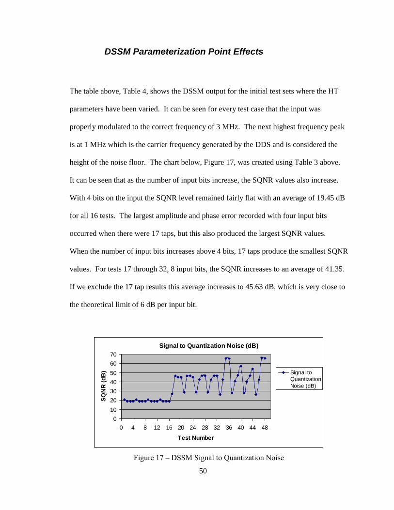
50
DSSM Parameterization Point Effects
The table above, Table 4, shows the DSSM output for the initial test sets where the HT
parameters have been varied. It can be seen for every test case that the input was
properly modulated to the correct frequency of 3 MHz. The next highest frequency peak
is at 1 MHz which is the carrier frequency generated by the DDS and is considered the
height of the noise floor. The chart below, Figure 17, was created using Table 3 above.
It can be seen that as the number of input bits increase, the SQNR values also increase.
With 4 bits on the input the SQNR level remained fairly flat with an average of 19.45 dB
for all 16 tests. The largest amplitude and phase error recorded with four input bits
occurred when there were 17 taps, but this also produced the largest SQNR values.
When the number of input bits increases above 4 bits, 17 taps produce the smallest SQNR
values. For tests 17 through 32, 8 input bits, the SQNR increases to an average of 41.35.
If we exclude the 17 tap results this average increases to 45.63 dB, which is very close to
the theoretical limit of 6 dB per input bit.
Signal to Quantization Noise (dB)
0
10
20
30
40
50
60
70
0 4 8 12 16 20 24 28 32 36 40 44 48
Test Number
SQ
NR
(d
B) Signal to
Quantization
Noise (dB)
Figure 17 – DSSM Signal to Quantization Noise

51
These tests show functionality of the DSSM and its components. The HT was able to
create a quadrature, Q, signal that was on average 90 degrees out of phase with the input
signal while maintaining the magnitude. The signal generator was able to create the
carrier signal for modulation without any magnitude or phase error and very reasonable
SQNR values. The input was modulated to the proper frequency with one sideband and
carrier signal eliminated creating a single sideband signal at the output. Additional test
results follow that check the DSSM’s functionality with two tone input, the affects of
windowing the Hilbert transform coefficients, and input frequency sweeps.
It is also important to note that with a low number of input bits and taps overflow did
occur. This was seen in the HT output data when the quadrature signal was leading the
in-phase signal, instead of lagging. The HT scaling factor (SC) was reduced in order to
correct for this problem.
Two tone input
This test was completed to verify the ability of the DSSM to accept two input signals and
properly modulate both of them. In the table below, Table 5, the left side has the input
parameters and the right side has the output data. In each test the input signals were up
converted so the expected output frequencies are the input plus the carrier frequency for
both tones. It can be seen that in each test both input frequencies were properly
modulated. The high spur signals are at the carrier frequency which is expected, except
for test number 136. The high spur signal is at the lower sideband of the modulated 11
MHz input instead of at 10 MHz; the next highest spur signal was -42.39 dB at 10 MHz.
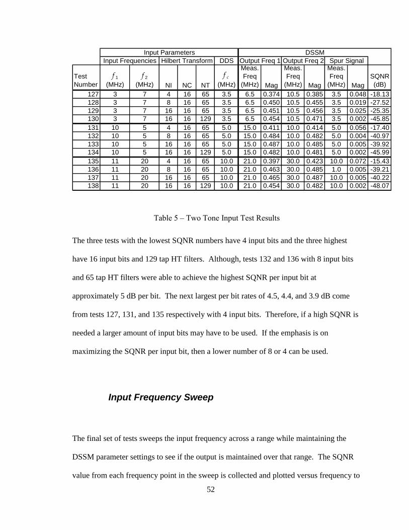
52
DDS
Test
Number
f 1
(MHz)
f 2
(MHz) NI NC NT
f c(MHz)
Meas.
Freq
(MHz) Mag
Meas.
Freq
(MHz) Mag
Meas.
Freq
(MHz) Mag
SQNR
(dB)
127 3 7 4 16 65 3.5 6.5 0.374 10.5 0.385 3.5 0.048 -18.13
128 3 7 8 16 65 3.5 6.5 0.450 10.5 0.455 3.5 0.019 -27.52
129 3 7 16 16 65 3.5 6.5 0.451 10.5 0.456 3.5 0.025 -25.35
130 3 7 16 16 129 3.5 6.5 0.454 10.5 0.471 3.5 0.002 -45.85
131 10 5 4 16 65 5.0 15.0 0.411 10.0 0.414 5.0 0.056 -17.40
132 10 5 8 16 65 5.0 15.0 0.484 10.0 0.482 5.0 0.004 -40.97
133 10 5 16 16 65 5.0 15.0 0.487 10.0 0.485 5.0 0.005 -39.92
134 10 5 16 16 129 5.0 15.0 0.482 10.0 0.481 5.0 0.002 -45.99
135 11 20 4 16 65 10.0 21.0 0.397 30.0 0.423 10.0 0.072 -15.43
136 11 20 8 16 65 10.0 21.0 0.463 30.0 0.485 1.0 0.005 -39.21
137 11 20 16 16 65 10.0 21.0 0.465 30.0 0.487 10.0 0.005 -40.22
138 11 20 16 16 129 10.0 21.0 0.454 30.0 0.482 10.0 0.002 -48.07
Input Parameters DSSM
Input Frequencies Hilbert Transform Output Freq 1 Output Freq 2 Spur Signal
Table 5 – Two Tone Input Test Results
The three tests with the lowest SQNR numbers have 4 input bits and the three highest
have 16 input bits and 129 tap HT filters. Although, tests 132 and 136 with 8 input bits
and 65 tap HT filters were able to achieve the highest SQNR per input bit at
approximately 5 dB per bit. The next largest per bit rates of 4.5, 4.4, and 3.9 dB come
from tests 127, 131, and 135 respectively with 4 input bits. Therefore, if a high SQNR is
needed a larger amount of input bits may have to be used. If the emphasis is on
maximizing the SQNR per input bit, then a lower number of 8 or 4 can be used.
Input Frequency Sweep
The final set of tests sweeps the input frequency across a range while maintaining the
DSSM parameter settings to see if the output is maintained over that range. The SQNR
value from each frequency point in the sweep is collected and plotted versus frequency to

53
show the variation and as with any filter there is expected to be some ripple across the
passband. The input frequency is swept from 3 – 17 MHz at step increments of at
0.05fs/2, 40 MHz sampling frequency, and 2.5 MHz carrier frequency. In actual
hardware implementation the number of filter taps is generally low due to space
requirement so in this test the values are kept below 25; 9, 13, 17, and 25.
The graph below, Figure 18, shows the DSSM SQNR results for each HT tap value
where the number of input and HT coefficient bits is 4. The average SQNR for the 9, 13,
17, and 25 tap values is 17.42, 16.59, 16.75, and 16.8 dB, respectively.
5
7
9
11
13
15
17
19
21
23
25
3 4 5 6 7 8 9 10 11 12 13 14 15 16 17
Frequency (MHz)
Ma
gn
itu
de
(d
B)
9 Taps
13 Taps
17 Taps
25 Taps
DSSM Output SQNR
4 Input & HT Coefficient Bits
Figure 18 – DSSM SQNR Input Frequency Sweep, 4 Input & Coefficient bits
The average SQNR values were expected to increase as the number of taps increased but
this is not the case. The decrease in SQNR averages with the increase in the tap values is
caused by quantization error of the end tap values. The table below, Table 6, lists the tap
number, floating point tap value, floating point scaled tap value, and the truncated scaled
value for a 25 tap filter with 4 coefficient bits and a scaling value of 6. These values are

54
the same for the 9, 13, and 17 tap filter centered at the ±0.6366 floating point HT
coefficient values and minus the endpoint values depending on the number of taps.
Tap
Floating Point
HT Coefficients
Floating Point Scaled
HT Coefficients
Truncated
HT Coefficients
1 -0.0579 -0.3472 0
3 -0.0707 -0.4244 0
5 -0.0909 -0.5457 -1
7 -0.1273 -0.7639 -1
9 -0.2122 -1.2732 -1
11 -0.6366 -3.8197 -4
13 0.6366 3.8197 4
15 0.2122 1.2732 1
17 0.1273 0.7639 1
19 0.0909 0.5457 1
21 0.0707 0.4244 0
23 0.0579 0.3472 0
Table 6 – Truncated Hilbert Transform Coefficients for 4 bits
The maximum truncated value is ±4 with 4 HT coefficient bits which does not leave
many quantization levels for the endpoints as they are forced to zero and one. The filter
with the lowest number of taps, 9, has effectively 4 tap values and each one has a
significant value but after 17 taps, all the end point tap values are zero.
The same test was performed for 8 input and HT coefficient bits. At several of the
frequency points in the sweep overflow had occurred in the HT filter. To correct for this
problem the scaling factor, equation 27, was further reduced by 18. The average SQNR
for the 9, 13, 17, and 25 tap values is 26.52, 23.22, 21.42, and 20 dB, respectively.

55
10
15
20
25
30
35
40
45
50
3 4 5 6 7 8 9 10 11 12 13 14 15 16 17
Frequency (MHz)
Ma
gn
itu
de
(d
B) 9 Taps
13 Taps
17 Taps
25 Taps
DSSM Output SQNR
8 Input & HT Coefficient Bits
Figure 19 – DSSM SQNR Input Frequency Sweep, 8 Input & Coefficient bits
The error between the floating and fixed point HT coefficients was then calculated to get
a better understanding of affects of the scaling factor, SC. Each floating point tap value
was multiplied by SC and compared with the truncated HT coefficient. The error is
taken as the absolute difference between those values. The total error for a 25 tap filter
with 8 HT coefficient bits is 2.72, Table 7 below.
Tap
Floating
Point
Scaled
Floating
Point Fixed Point Error
1 -0.0579 -7.29 -7 0.29
3 -0.0707 -8.91 -9 0.09
5 -0.0909 -11.46 -11 0.46
7 -0.1273 -16.04 -16 0.04
9 -0.2122 -26.74 -27 0.26
11 -0.6366 -80.21 -80 0.21
13 0.6366 80.21 80 0.21
15 0.2122 26.74 27 0.26
17 0.1273 16.04 16 0.04
19 0.0909 11.46 11 0.46
21 0.0707 8.91 9 0.09
23 0.0579 7.29 7 0.29
Table 7 – Hilbert transform coefficient error; 8 bits, 25 taps

56
V. Conclusion
This design improves the state of the art by providing an inexpensive, long term,
portable, and parameterizable VHDL solution which allows for rapid design and redesign
of DSSMs. And as technology changes and ADC speeds increase this code transitions
with it and allows designers to quickly design, re-design, prototype, and layout for ASIC
fabrication. The digital single sideband modulator implemented using a Hilbert
transform rapidly delivers digital circuits for FPGA or ASIC applications.
Future Work
The true test of any design is through actual implementation in a selected technology
where it can undergo real world conditions. Through implementation the physical size
requirements would be calculated which could then be further explored for tradeoffs such
as the number of Hilbert transform taps or input or Hilbert transform coefficient bit size
versus accuracy.
During simulation overflow occurred in the Hilbert transform quadrature signal which
was apparent as the peak values rolled over. This was manually corrected for by
reducing the scaling factor, equation 27 in section 3.1. It needs to be low enough to
prevent overflow but high enough to enable the Q signal to reach the full scale two’s
compliment values. An automated approach should be considered in the selection of the
scaling factor to prevent overflow while realizing the full scale values to maximize the

57
signal to quantization noise. A larger number of HT filter taps could also minimize this
issue but for the purposes of this research the values were kept to small realizable
numbers.

58
Appendix A
VHDL Source Code
Hilbert Transform
------------------------------------------------------------------
library IEEE;
use IEEE.STD_LOGIC_1164.ALL;
use IEEE.STD_LOGIC_ARITH.ALL;
use IEEE.STD_LOGIC_SIGNED.ALL;
-- pragma synthesis_off
use IEEE.MATH_REAL.ALL;
use IEEE.STD_LOGIC_TEXTIO.ALL;
use STD.TEXTIO.ALL;
-- pragma synthesis_on
------------------------------------------------------------------
------------------------------------------------------------------
entity HILBERT is
generic ( -- Prog user fills in desired constraints
NI : integer; -- # of input bits
NC : integer; -- coefficient bit size
NT : integer; -- # of taps -- (NT-1)/2 must be even
NE : integer; -- extra bits for + -- set to ceil(log_2(((NT-1)/2)))
WIN : integer); -- window selection for HT
port (
SI : in std_logic_vector(NI-1 downto 0); --input signal
CLK: in std_logic; --Clock
SD : out std_logic_vector(NI-1 downto 0); --(I) original 'delayed' output signal
SO : out std_logic_vector(NI-1 downto 0)); --(Q) modified output signal
end HILBERT;
------------------------------------------------------------------
------------------------------------------------------------------
architecture Behavioral of HILBERT is
----------------------------------------------------------------
--array of size NT to hold HT coefficients of size NC
type HTC_ARRAY is array (NT-1 downto 0) of std_logic_vector(NC-1 downto 0);
--array of size NT to hold input bit coefficients of size NI
type INPUT_ARRAY_TYPE is array (NT-1 downto 0) of std_logic_vector(NI-1
downto 0);
type III_TYPE is array (0 to NT) of integer;
type A_ARRAY_TYPE is array (NT-1 downto 0) of integer;
type R_ARRAY_TYPE is array (NT-1 downto 0) of real;

59
signal COEFF_ARRAY: HTC_ARRAY; --hold HT coefficients
signal INPUT_ARRAY: INPUT_ARRAY_TYPE; --hold input
signal III : III_TYPE;
signal A: A_ARRAY_TYPE;
signal SR_ARRAY,WC: R_ARRAY_TYPE := (0.0, others => 0.0);
signal SC : real := 0.0;
constant PI : real := 3.14159265; -- pi
file OUT_FILE: text is out "coefficients.xls";
----------------------------------------------------------------
----------------------------------------------------------------
begin
----------------------------------------------------------------
-- Capture Inputs in a clocked array ... Input signal SI
INPUT: process (CLK)
begin
if rising_edge(CLK) then
for n in NT-1 downto 1 loop
INPUT_ARRAY(n)<=INPUT_ARRAY(n-1);
end loop;
INPUT_ARRAY(0)<=SI;
end if;
end process INPUT;
----------------------------------------------------------------
-- delayed input to match output
DELAY: process (CLK,INPUT_ARRAY)
begin
if rising_edge(CLK) then
SD <= INPUT_ARRAY((NT-1)/2);
end if;
end process DELAY;
----------------------------------------------------------------
SC <= real((2**NC)/2)-2.0;
----------------------------------------------------------------
--Generate the index for coefficients
III(0) <= 0;
Hilbert_Index: for I in 0 to NT-1 generate
III(I+1) <= III(I)+1; -- III has the same value as index I
end generate Hilbert_Index;
----------------------------------------------------------------
WIN_Coef: for H in 0 to NT-1 generate
WC(H)<=1.0 --Rectangular
when WIN=1 else

60
2.0*real(H)/(real(NT)-1.0) --Bartlett
when (WIN=2 and H<=(NT-1)/2) else
2.0-(2.0*real(H)/(real(NT)-1.0)) --Bartlett
when (WIN=2 and H>(NT-1)/2) else
0.5-0.5*cos(2.0*PI*real(H)/(real(NT)-1.0)) --Hanning
when WIN=3 else
0.54-0.46*cos(2.0*PI*real(H)/(real(NT)-1.0)) --Hamming
when WIN=4 else
0.42-0.5*cos(2.0*PI*real(H)/(real(NT)-1.0))+ --Blackman
0.08*cos(4.0*PI*real(H)/(real(NT)-1.0));
end generate WIN_Coef;
----------------------------------------------------------------
--Generate the Hilbert Coefficients
Hilbert_Coefs: for I in 0 to NT-1 generate
hil_cell: if (I rem 2 ) /= 0 generate
A(I) <=
integer(
WC(I)*SC*2.0/PI/
real(III(I)-((NT-1)/2))*
sin(PI*real(III(I)-((NT-1)/2))/2.0)*
sin(PI*real(III(I)-((NT-1)/2))/2.0)
);
COEFF_ARRAY(I)<=conv_std_logic_vector(A(I),NC);
SR_ARRAY(I) <=
WC(I)*2.0/PI/
real(III(I)-((NT-1)/2))*
sin(PI*real(III(I)-((NT-1)/2))/2.0)*
sin(PI*real(III(I)-((NT-1)/2))/2.0) ;
end generate hil_cell;
end generate Hilbert_Coefs;
----------------------------------------------------------------
process (CLK,INPUT_ARRAY)
variable MULT_VAL: std_logic_vector(NC+NI+NE-1 downto 0);
variable SI_SUM: std_logic_vector(NC+NI+NE-1 downto 0);
variable SR_SUM: real;
begin
if rising_edge(CLK) then
SR_SUM:=0.0; -- real values
SI_SUM:= (others=>'0');
--Enter incoming data into array & multiply by HCoeffs

61
for n in NT-1 downto 0 loop
if (n rem 2) /= 0 then
MULT_VAL(NC+NI-1 downto 0) := INPUT_ARRAY(n)*COEFF_ARRAY(n);
-- NI+NC bits
MULT_VAL(NC+NI+NE-1 downto NC+NI) := (others => MULT_VAL(NC+NI-
1)); -- sign extend
SI_SUM := SI_SUM + MULT_VAL(NC+NI-1 downto 0); -- clac integer final
SR_SUM := SR_SUM + real(conv_integer(MULT_VAL(NC+NI-1 downto 0)));
-- clac real final
end if;
end loop;
SO <= SI_SUM(NC+NI-2 downto NC-1);
end if;
end process;
----------------------------------------------------------------
process(III)
variable OUT_LINE: line;
variable COEF_VALUE: real;
begin
if III(NT) = NT then
for I in 0 to NT-1 loop
if (I rem 2) /= 0 then
COEF_VALUE := 2.0/PI/(real(I)-real((NT-1)/2))*
sin(PI*real(I-(NT-1)/2)/2.0)*
sin(PI*real(I-(NT-1)/2)/2.0);
--start of OUT_FILE 'coefficients.txt'
if I = 1 then
write(OUT_LINE,string'("I III COEF_VALUE SR_ARRAY Ai/SC Ai C_A C_A
C_A/SC WIN WC"));
writeline(OUT_FILE, OUT_LINE);
end if;
write(OUT_LINE, I);
write(OUT_LINE,string'(" "));
write(OUT_LINE, III(I));
write(OUT_LINE,string'(" "));
write(OUT_LINE, COEF_VALUE);
write(OUT_LINE,string'(" "));
write(OUT_LINE, SR_ARRAY(I));
write(OUT_LINE,string'(" "));
write(OUT_LINE, real(A(I))/SC);
write(OUT_LINE,string'(" "));
write(OUT_LINE, A(I));
write(OUT_LINE,string'(" "));
write(OUT_LINE, COEFF_ARRAY(I));
write(OUT_LINE,string'(" "));

62
write(OUT_LINE, conv_integer(COEFF_ARRAY(I)));
write(OUT_LINE,string'(" "));
write(OUT_LINE, real(conv_integer(COEFF_ARRAY(I)))/SC);
write(OUT_LINE,string'(" "));
write(OUT_LINE, WIN);
write(OUT_LINE,string'(" "));
write(OUT_LINE, WC(I));
writeline(OUT_FILE, OUT_LINE);
end if;
end loop;
end if;
end process;
----------------------------------------------------------------
end Behavioral;
Sine and Cosine Wave Generation
------------------------------------------------------------------
library IEEE;
use IEEE.STD_LOGIC_1164.ALL;
use IEEE.STD_LOGIC_ARITH.ALL;
use IEEE.STD_LOGIC_SIGNED.ALL;
use IEEE.MATH_REAL.ALL;
use IEEE.STD_LOGIC_TEXTIO.ALL;
use STD.TEXTIO.ALL;
------------------------------------------------------------------
------------------------------------------------------------------
entity HS_Switch is
generic (
NI : integer; -- # of input bits
NC : integer; -- # of coefficient bits
RG : integer; -- 1/4 wave granularity
R_STEP : integer); -- # of ROM address steps to skip
port (
CLK: in std_logic; --Clock
SINE : out std_logic_vector(NI-1 downto 0); -- Sine wave output
COSINE : out std_logic_vector(NI-1 downto 0)); -- Cosine wave output
end HS_Switch;
------------------------------------------------------------------
architecture Behavioral of HS_SWITCH is
----------------------------------------------------------------
type QW is array (0 to RG) of std_logic_vector(NI-1 downto 0);
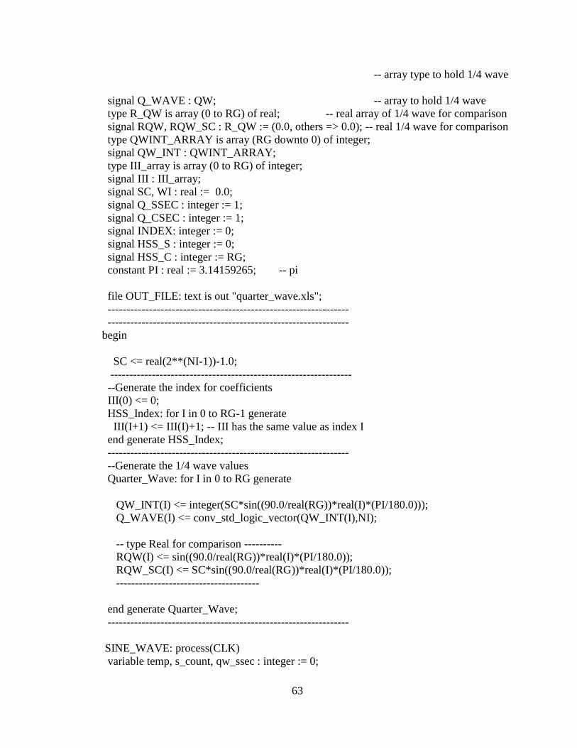
63
-- array type to hold 1/4 wave
signal Q_WAVE : QW; -- array to hold 1/4 wave
type R_QW is array (0 to RG) of real; -- real array of 1/4 wave for comparison
signal RQW, RQW_SC : R_QW := (0.0, others => 0.0); -- real 1/4 wave for comparison
type QWINT_ARRAY is array (RG downto 0) of integer;
signal QW_INT : QWINT_ARRAY;
type III_array is array (0 to RG) of integer;
signal III : III_array;
signal SC, WI : real := 0.0;
signal Q_SSEC : integer := 1;
signal Q_CSEC : integer := 1;
signal INDEX: integer := 0;
signal HSS_S : integer := 0;
signal HSS_C : integer := RG;
constant PI : real := 3.14159265; -- pi
file OUT_FILE: text is out "quarter_wave.xls";
----------------------------------------------------------------
----------------------------------------------------------------
begin
SC <= real(2**(NI-1))-1.0;
----------------------------------------------------------------
--Generate the index for coefficients
III(0) <= 0;
HSS_Index: for I in 0 to RG-1 generate
III(I+1) <= III(I)+1; -- III has the same value as index I
end generate HSS_Index;
----------------------------------------------------------------
--Generate the 1/4 wave values
Quarter_Wave: for I in 0 to RG generate
QW_INT(I) <= integer(SC*sin((90.0/real(RG))*real(I)*(PI/180.0)));
Q_WAVE(I) <= conv_std_logic_vector(QW_INT(I),NI);
-- type Real for comparison ----------
RQW(I) <= sin((90.0/real(RG))*real(I)*(PI/180.0));
RQW_SC(I) <= SC*sin((90.0/real(RG))*real(I)*(PI/180.0));
--------------------------------------
end generate Quarter_Wave;
----------------------------------------------------------------
SINE_WAVE: process(CLK)
variable temp, s_count, qw_ssec : integer := 0;

64
begin
s_count := HSS_S; -- 1/4 wave array index counter
qw_ssec := Q_SSEC; -- 1/4 wave section
if CLK'event and CLK='1'then
-- if CLK'event then
if qw_ssec=1 or qw_ssec=3 then -- count up or down
s_count := s_count + R_STEP;
else
s_count := s_count - R_STEP;
end if;
if s_count>=0 and s_count<=RG then --if array index is w/in bound of RG
if qw_ssec=1 or qw_ssec=2 then
SINE <= Q_WAVE(s_count);
if qw_ssec = 2 and s_count = 0 then
qw_ssec := 3;
end if;
else
SINE <= -Q_WAVE(s_count);
if qw_ssec = 4 and s_count = 0 then
qw_ssec := 1;
end if;
end if;
elsif qw_ssec=1 or qw_ssec=3 then
temp := s_count - RG;
s_count := RG - temp;
if qw_ssec = 1 then
SINE <= Q_WAVE(s_count);
else
SINE <= -Q_WAVE(abs(s_count));
end if;
qw_ssec := qw_ssec + 1;
if (s_count=0 or s_count=RG) and R_STEP>RG then
qw_ssec := qw_ssec+1;
end if;
else -- qw_ssec=2 or 4 & outside of the 1/4 wave section
temp := abs(s_count) - RG;
s_count := RG - abs(temp);
if qw_ssec = 2 then
SINE <= -Q_WAVE(s_count);
else
SINE <= Q_WAVE(s_count);
end if;

65
qw_ssec := qw_ssec +1;
if (s_count=0 or s_count=RG) and R_STEP>RG then
qw_ssec := qw_ssec+1;
end if;
end if;
if qw_ssec > 4 then
qw_ssec := qw_ssec mod 4;
end if;
HSS_S <= s_count;
Q_SSEC <= qw_ssec;
end if;
end process SINE_WAVE;
COSINE_WAVE: process(CLK)
variable temp, c_count, qw_csec : integer := 0;
begin
c_count := HSS_C;
qw_csec := Q_CSEC;
if CLK'event and CLK='1'then
-- if CLK'event then
if qw_csec=2 or qw_csec=4 then
c_count := c_count + R_STEP;
else
c_count := c_count - R_STEP;
end if;
if c_count>=0 and c_count<=RG then
if qw_csec=1 or qw_csec=4 then
COSINE <= Q_WAVE(c_count);
if qw_csec = 1 and c_count = 0 then
qw_csec := 2;
end if;
else
COSINE <= -Q_WAVE(c_count);
if qw_csec = 3 and c_count = 0 then
qw_csec := 4;
end if;
end if;
elsif qw_csec=2 or qw_csec=4 then
temp := c_count - RG;
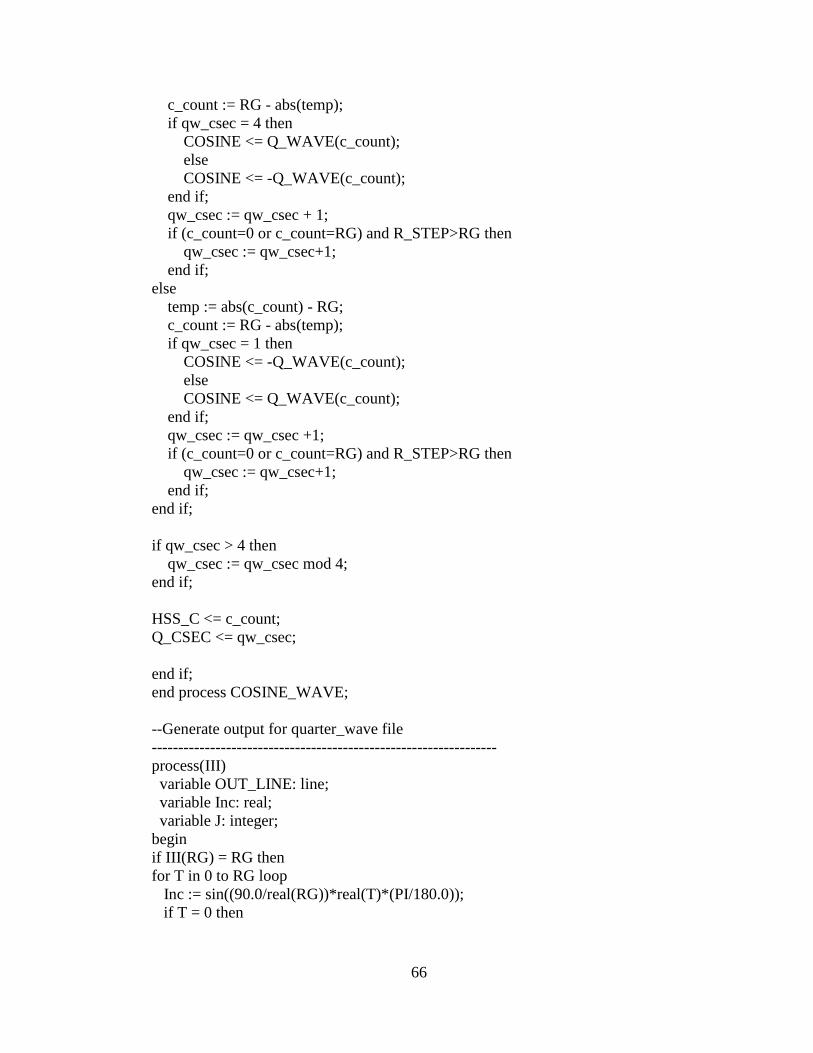
66
c_count := RG - abs(temp);
if qw_csec = 4 then
COSINE <= Q_WAVE(c_count);
else
COSINE <= -Q_WAVE(c_count);
end if;
qw_csec := qw_csec + 1;
if (c_count=0 or c_count=RG) and R_STEP>RG then
qw_csec := qw_csec+1;
end if;
else
temp := abs(c_count) - RG;
c_count := RG - abs(temp);
if qw_csec = 1 then
COSINE <= -Q_WAVE(c_count);
else
COSINE <= Q_WAVE(c_count);
end if;
qw_csec := qw_csec +1;
if (c_count=0 or c_count=RG) and R_STEP>RG then
qw_csec := qw_csec+1;
end if;
end if;
if qw_csec > 4 then
qw_csec := qw_csec mod 4;
end if;
HSS_C <= c_count;
Q_CSEC <= qw_csec;
end if;
end process COSINE_WAVE;
--Generate output for quarter_wave file
-----------------------------------------------------------------
process(III)
variable OUT_LINE: line;
variable Inc: real;
variable J: integer;
begin
if III(RG) = RG then
for T in 0 to RG loop
Inc := sin((90.0/real(RG))*real(T)*(PI/180.0));
if T = 0 then

67
write(OUT_LINE,string'("Index SC Incrament RQW RQW_SC QW_INT Q_WAVE
Q_WAVE"));
write(OUT_LINE,string'(" "));
writeline(OUT_FILE, OUT_LINE);
end if;
write(OUT_LINE, T);
write(OUT_LINE,string'(" "));
write(OUT_LINE, SC);
write(OUT_LINE,string'(" "));
write(OUT_LINE, Inc);
write(OUT_LINE,string'(" "));
write(OUT_LINE, RQW(T));
write(OUT_LINE,string'(" "));
write(OUT_LINE, RQW_SC(T));
write(OUT_LINE,string'(" "));
write(OUT_LINE, QW_INT(T));
write(OUT_LINE,string'(" "));
write(OUT_LINE, conv_integer(Q_WAVE(T)));
write(OUT_LINE,string'(" "));
J:= NI-1;
S_W: while J > -1 loop
write(OUT_LINE,conv_integer(Q_WAVE(T)(J)));
J := J - 1;
end loop S_W;
writeline(OUT_FILE, OUT_LINE);
end loop;
end if;
end process;
----------------------------------------------------------------
end Behavioral;
Multiply and Adder Block
------------------------------------------------------------------
library IEEE;
use IEEE.STD_LOGIC_1164.ALL;
use IEEE.STD_LOGIC_ARITH.ALL;
use IEEE.STD_LOGIC_SIGNED.ALL;
use IEEE.MATH_REAL.ALL;
use IEEE.STD_LOGIC_TEXTIO.ALL;
use STD.TEXTIO.ALL;
------------------------------------------------------------------
------------------------------------------------------------------
entity DSSM_OUT is

68
generic (
NI : integer); -- # of input bits
port (
CLK: in std_logic; --Clock
SD : in std_logic_vector(NI-1 downto 0); --(I) original 'delayed' output signal
SO : in std_logic_vector(NI-1 downto 0); --(Q) modified output signal
SINE : in std_logic_vector(NI-1 downto 0); -- Sine wave output
COSINE : in std_logic_vector(NI-1 downto 0); -- Cosine wave output
DSSM : out std_logic_vector(NI-1 downto 0));
end DSSM_OUT;
------------------------------------------------------------------
architecture Behavioral of DSSM_OUT is
------------------------------------------------------------------
begin
FINAL_OUT: process(CLK)
variable MIX: std_logic_vector((2*NI)-1 downto 0);
begin
MIX:=(SD*COSINE)-(SO*SINE);
DSSM <= MIX((2*NI)-2 downto (NI-1));
end process FINAL_OUT;
end Behavioral;
Testbench
library ieee, WORK;
use std.textio.all;
use ieee.std_logic_1164.all;
use ieee.std_logic_arith.all;
use ieee.std_logic_signed.all;
use ieee.math_real.all;
entity TB_DSSM is
generic (
NI : integer := 4; -- number of input bits
NC : integer := 4; -- number of coeff bits

69
NT : integer := 9; -- # of taps -- (NT-1)/2 must be even
NE : integer := 2; -- extra bits for + -- set to ceil(log_2(((NT-1)/2)))
WIN : integer := 1; -- Window selction for HT
RG : integer := 2; -- 1/4 wave granularity
R_STEP : integer := 1; -- ROM address step
-- NOTE -- R_STEP must be <= RG
N_ITS : integer := 10001; -- number of test sets
CP : time := 25.0ns;
CPR : real := 25.0e-9;
f1 : real := 3.0e6;
f2 : real := 3.0e6;
P1 : real := 0.0; -- [dB] power levels
P2 : real := 0.0 -- [dB] power levels
);
end ;
architecture TB of TB_DSSM is
constant PI : real := 3.14159265; -- pi
file OUT_FILE: text is out "sim_out.xls";
file OUT_FILE2: text is out "sim_out_IQ.xls";
file OUT_FILE3: text is out "HSS_OUT.xls";
file OUT_FILE4: text is out "DSSM_OUT.xls";
file OUT_FILE5: text is out "Spectral_OUT.xls";
component HILBERT
generic (
NI : integer; -- # of input bits
NC : integer; -- coefficient bit size
NT : integer; -- (NT-1)/2 must be even
NE : integer; -- set to ceil(log_2(((NT-1)/2)))
WIN: integer); -- window selection for HT
port (
SI : in std_logic_vector(NI-1 downto 0); --input signal
CLK: in std_logic; --Clock
SD : out std_logic_vector(NI-1 downto 0); --(I) original 'delayed' output signal
SO : out std_logic_vector(NI-1 downto 0)); --(Q) modified output signal
end component;
component HS_Switch
generic (
NI : integer; -- # of input bits
NC : integer; -- coefficient bit size
RG : integer; -- 1/4 wave granularity
R_STEP : integer); -- ROM address step
port (
CLK: in std_logic; --Clock

70
SINE : out std_logic_vector(NI-1 downto 0); -- SINE wave
COSINE : out std_logic_vector(NI-1 downto 0)); -- COSINE wave
end component;
component DSSM_OUT
generic (
NI : integer); -- # of input bits
port (
CLK: in std_logic; --Clock
SD : in std_logic_vector(NI-1 downto 0); --(I) original 'delayed' output signal
SO : in std_logic_vector(NI-1 downto 0); --(Q) modified output signal
SINE : in std_logic_vector(NI-1 downto 0); -- Sine wave output
COSINE : in std_logic_vector(NI-1 downto 0); -- Cosine wave output
DSSM : out std_logic_vector(NI-1 downto 0));
end component;
type TYPE_INPUT_ARRAY is array(0 to N_ITS) of std_logic_vector(NI-1 downto 0);
type TYPE_REAL_ARRAY is array(0 to N_ITS) of real;
type TYPE_QWAVAL is array (1 to 50)of real;
signal INPUT_V: TYPE_INPUT_ARRAY;
signal CLK : std_logic;
signal INDEX : integer := 0;
signal ADC, SO, SD, SINE, COSINE : std_logic_vector(NI-1 downto 0);
signal DSSM : std_logic_vector(NI-1 downto 0);
signal AmpAv1, PhaseAv1, RunAA, RunPA, RunWAA, RunWPA: real := 0.0; --Hold
1st diff value for averaging
signal SAA1, PA1, SAE1, PAE1:real:=0.0; -- Hold 1st values for averaging
signal AmpE1, PhaseE1, RunAE, RunPE : real := 0.0;
signal IWA_array, IWP_array, WGWA_array, WGWP_array : TYPE_QWAVAL :=
(0.0, others => 0.0);
signal VAD, VPD, VWAD, VWPD, RWAE, RWPE: real := 0.0;
signal Adiff, Pdiff, WGAdiff, WGPdiff:real:=0.0;
begin
COMP_HIL: HILBERT
generic map (NI=>NI,NC=>NC,NT=>NT,NE=>NE,WIN=>WIN)
port map (SI=>ADC,CLK=>CLK,SO=>SO,SD=>SD);
COMP_SWITCH: HS_Switch
generic map (NI=>NI,NC=>NC,RG=>RG,R_STEP=>R_STEP)
port map (CLK=>CLK,SINE=>SINE,COSINE=>COSINE);
COMP_MaA: DSSM_OUT
generic map (NI=>NI)
port map
(CLK=>CLK,SINE=>SINE,COSINE=>COSINE,SO=>SO,SD=>SD,DSSM=>DSSM);

71
CLK_PROC: process
begin
wait for CP/2;
CLK <= '0';
wait for CP/2;
CLK <= '1';
end process CLK_PROC;
INPUT: process(CLK)
variable Z:integer:=0;
begin
if CLK'event and CLK='1'then
ADC <= INPUT_V(INDEX);
if INDEX = N_ITS-1 then
INDEX <= 0;
else
INDEX <= INDEX + 1;
end if;
end if;
end process INPUT;
FFT_PROC: process
variable W1,W2,A1,A2,Amax,P_dym,fsample:real:=1.0; -- amplitudes
variable S_REAL,VAL_COMP,VAL_DIV : real;
variable H,J, K, npqw, WGQW: integer;
variable Iamp, Qamp, Ip, Qp, Amp_Err, Phase_Err:real:=0.0;
variable Samp, Camp, Soph, Coph, WGA_Err, WGP_Err:real:=0.0;
variable INPUT_R: TYPE_REAL_ARRAY;
variable S_VECTOR : TYPE_INPUT_ARRAY;
variable OUT_LINE: line;
variable freq, period_ofreq, PPP, WG_PPP, RAA, RPA: real := 0.0;
variable RWAA, RWPA: real :=0.0;
begin
fsample := 1.0/real(CPR);
---------------------------------------
--vvvvvvvvvvvvvvvvvvvvvvvvvvvvvvvvvvvvv
-- generate input data ---------------
P_dym := P1 - P2;
A2 := Amax / (1.0 + exp(P_dym/10.0));
A1 := Amax-A2;
W1 := 2.0 * PI * real(f1);
W2 := 2.0 * PI * real(f2);
--start of OUT_FILE 'sim_out.txt'

72
write(OUT_LINE,1.0/CPR);
write(OUT_LINE,string'(" "));
write(OUT_LINE,f1);
write(OUT_LINE,string'(" "));
write(OUT_LINE,A1);
write(OUT_LINE,string'(" "));
write(OUT_LINE,W1);
write(OUT_LINE,string'(" "));
write(OUT_LINE,f2);
write(OUT_LINE,string'(" "));
write(OUT_LINE,A2);
write(OUT_LINE,string'(" "));
write(OUT_LINE,W2);
writeline(OUT_FILE, OUT_LINE);
K:= 0;
WH_LOOPK0: while K < N_ITS-1 loop
S_REAL := A1*cos(W1*REAL(K)*CPR)+A2*cos(W2*REAL(K)*CPR);
-- n bit ADC
VAL_COMP := 0.0;
VAL_DIV := 0.0;
if S_REAL < VAL_COMP then S_VECTOR(K)(NI-1):='1';
VAL_DIV:=-0.5;
VAL_COMP:=-0.5;
else S_VECTOR(K)(NI-1):='0';
VAL_DIV:=0.5;
VAL_COMP:=0.5;
end if;
for IIII in 1 to NI-1 loop
if S_REAL < VAL_COMP then
S_VECTOR(K)(NI-1-IIII):='0';
VAL_DIV:=VAL_DIV/2.0;
VAL_COMP:=VAL_COMP-abs(VAL_DIV);
else -- S_REAL >= VAL_COMP
S_VECTOR(K)(NI-1-IIII):='1';
VAL_DIV:=VAL_DIV/2.0;
VAL_COMP:=VAL_COMP+abs(VAL_DIV);
end if;
end loop;
INPUT_V(K) <= S_VECTOR(K);
INPUT_R(K) := S_REAL;
K := K + 1;
end loop WH_LOOPK0;

73
--^^^^^^^^^^^^^^^^^^^^^^^^^^^^^^^^^^^^^^
K:= 0;
WH_LOOPK1: while K < N_ITS-1 loop
--I&Q Amplitude Calculation
Iamp:= real(conv_integer(SD))/(2.0**(NI-1));
Qamp:= real(conv_integer(SO))/(2.0**(NI-1));
--Sine & Cosine Amplitude Calculation
Samp:= real(conv_integer(Sine))/(2.0**(NI-1));
Camp:= real(conv_integer(Cosine))/(2.0**(NI-1));
--I&Q Phase Calculation
Ip := arcsin(Iamp)*(180.0/PI);
Qp := arccos(Qamp)*(180.0/PI);
--Sine & Cosine Phase Calculation
Soph := arcsin(Samp)*(180.0/PI);
Coph := arccos(Camp)*(180.0/PI);
----------------------------------------------------------------
--Generate array to hold 1/4 wave amplitude values for accuracy check
freq := f1;
if f2 > f1 then
freq := f2;
end if;
period_ofreq := 1.0/freq; -- find the period of the higher freq
PPP := period_ofreq/CPR; -- find the # of points/period
npqw := integer(PPP)/4; -- divide by 4 to get # of points/quarter wave
WG_PPP := (CPR*((real(RG)*4.0)/real(R_STEP)))/CPR; -- period of the WG Sin
& Cos / CP to get points per period
WGQW := integer(WG_PPP)/4;
if npqw < 1 then
npqw := 1;
else
for B in npqw downto 2 loop
IWA_array(B)<=IWA_array(B-1); -- I is leading & Q is lagging by 90 degrees
IWP_array(B)<=IWP_array(B-1);
end loop; -- so we store I wating for Q to catch up
end if;
if WGQW < 1 then
WGQW := 1;
else
for C in WGQW downto 2 loop
WGWA_array(C)<=WGWA_array(C-1); -- I is leading & Q is lagging by 90
degrees
WGWP_array(C)<=WGWP_array(C-1);
end loop;
end if;

74
IWA_array(1) <= Iamp;
IWP_array(1) <= Ip;
WGWA_array(1) <= Camp;
WGWP_array(1) <= Coph;
Adiff <= abs(Qamp - IWA_array(npqw));
Pdiff <= abs(Qp + IWP_array(npqw));
WGAdiff <= abs(Samp - WGWA_array(WGQW));
WGPdiff <= abs(Soph + WGWP_array(WGQW));
----------------------------------------------------------------
--Amplitude & Phase error for the I & Q Channel
if IWA_array(npqw) = 0.0 then Amp_Err := (abs(Qamp)*100.0);
elsif Qamp = 0.0 then Amp_Err := (abs(IWA_array(npqw))*100.0);
else Amp_Err := (abs(IWA_array(npqw)-Qamp)/abs(IWA_array(npqw))*100.0);
end if;
Phase_Err := ((abs(90.0 - Pdiff)/90.0)*100.0);
--**************************************--
--Amplitude & Phase error for the Sine & Cosine
if WGWA_array(WGQW) = 0.0 then WGA_Err := (abs(Samp)*100.0);
elsif Samp = 0.0 then WGA_Err := (abs(WGWA_array(WGQW))*100.0);
else WGA_Err := (abs(WGWA_array(WGQW)-
Samp)/abs(WGWA_array(WGQW))*100.0);
end if;
WGP_Err := ((abs(90.0 - WGPdiff)/90.0)*100.0);
--**************************************--
--Running Averages for Amplitude and Phase
--&&&&&&&&&&&&&&&&&&&&&&&&&&&&&&&&&&&&&&--
--STD Deviation for Amplitude and Phase
if K = 500 then
AmpAv1 <= Adiff; PhaseAv1 <= Pdiff; --I & Q Avg diff
AmpE1 <= Amp_Err; PhaseE1 <= Phase_Err; --I & Q Avg err
SAA1 <= WGAdiff; PA1 <= WGPdiff; --S & C Avg diff
SAE1 <= WGA_Err; PAE1 <= WGP_Err; --S & C Avg err
elsif K = 501 then
RAA := (Adiff + AmpAv1)/2.0; --Avg amp diff
RPA := (Pdiff + PhaseAv1)/2.0; --Avg pha diff
RunAE <= (Amp_Err + AmpE1)/2.0; --Avg amp err
RunPE <= (Phase_Err + PhaseE1)/2.0; --Avg pha err
RWAA := (WGAdiff + SAA1)/2.0; --Avg amp diff
RWPA := (WGPdiff + PA1)/2.0; --Avg pha diff
RWAE <= (WGA_Err + SAE1)/2.0; --Avg amp err
RWPE <= (WGP_Err + PAE1)/2.0; --Avg pha err
--Variance of the I&Q amplitude difference
VAD <= (1.0/(real(K)+1.0))*((AmpAv1-RAA)**2.0+(Adiff-RAA)**2.0);
--Variance of the I&Q phase difference

75
VPD <= (1.0/(real(K)+1.0))*((PhaseAv1-RPA)**2.0+(Pdiff-RPA)**2.0);
--Variance of the S&C amplitude difference
VWAD <= (1.0/(real(K)+1.0))*((SAA1-RWAA)**2.0+(WGAdiff-
RWAA)**2.0);
--Variance of the S&C phase difference
VWPD <= (1.0/(real(K)+1.0))*((PA1-RWPA)**2.0+(WGPdiff-RWPA)**2.0);
elsif K > 501 then
-- I&Q Values
RAA := (Adiff+real(K)*RunAA)/(real(K)+1.0); --Avg amp diff
RPA := (Pdiff+real(K)*RunPA)/(real(K)+1.0); --Avg pha diff
RunAE <= (Amp_Err+real(K)*RunAE)/(real(K)+1.0); --Avg amp err
RunPE <= (Phase_Err+real(K)*RunPE)/(real(K)+1.0); --Avg pha err
--Variance of the I&Q amplitude difference
VAD <=
((Adiff**2.0)/(real(K)+1.0))+(real(K)/(real(K)+1.0))*(VAD+RunAA**2.0)-
(RAA**2.0);
--Variance of the I&Q phase difference
VPD <=
((Pdiff**2.0)/(real(K)+1.0))+(real(K)/(real(K)+1.0))*(VPD+RunPA**2.0)-(RPA**2.0);
-- S&C Values
RWAA := (WGAdiff+real(K)*RunWAA)/(real(K)+1.0); --Avg amp diff
RWPA := (WGPdiff+real(K)*RunWPA)/(real(K)+1.0); --Avg pha diff
RWAE <= (WGA_Err+real(K)*RWAE)/(real(K)+1.0); --Avg amp err
RWPE <= (WGP_Err+real(K)*RWPE)/(real(K)+1.0); --Avg pha err
--Variance of the I&Q amplitude difference
VWAD <=
((WGAdiff**2.0)/(real(K)+1.0))+(real(K)/(real(K)+1.0))*(VWAD+RunWAA**2.0)-
(RWAA**2.0);
--Variance of the I&Q phase difference
VWPD <=
((WGPdiff**2.0)/(real(K)+1.0))+(real(K)/(real(K)+1.0))*(VWPD+RunWPA**2.0)-
(RWPA**2.0);
end if;
RunAA <= RAA;
RunPA <= RPA;
RunWAA <= RWAA;
RunWPA <= RWPA;
--continuation of OUT_FILE 'sim_out.txt'
if K = 0 then
write(OUT_LINE,string'("INDEX INPUT_R INPUT_V INPUT_V ADC SD SD
SO SO SO Iamp Qamp Adiff Ip Qp Pdiff Amp_Err Phase_Err RunAA RunAP RunAE
RunPE VAD VPD"));
write(OUT_LINE,string'(" "));
writeline(OUT_FILE, OUT_LINE);

76
end if;
write(OUT_LINE,INDEX);
write(OUT_LINE,string'(" "));
write(OUT_LINE,INPUT_R(K));
write(OUT_LINE,string'(" "));
J:= NI-1;WH_LOOPJ2: while J > -1 loop
write(OUT_LINE,conv_integer(INPUT_V(K)(J)));
J := J - 1;
end loop WH_LOOPJ2;
write(OUT_LINE,string'(" "));
write(OUT_LINE,conv_integer(INPUT_V(K)));
write(OUT_LINE,string'(" "));
write(OUT_LINE,conv_integer(ADC));
write(OUT_LINE,string'(" "));
write(OUT_LINE,conv_integer(SD));
write(OUT_LINE,string'(" "));
write(OUT_LINE,((real(conv_integer(SD)))*2.0**(-(real(NI)-1.0))));
write(OUT_LINE,string'(" "));
for J in NI-1 downto 0 loop
write(OUT_LINE,conv_integer(SO(J)));
end loop;
write(OUT_LINE,string'(" "));
write(OUT_LINE,conv_integer(SO));
write(OUT_LINE,string'(" "));
write(OUT_LINE,((real(conv_integer(SO)))*2.0**(-(real(NI)-1.0))));
write(OUT_LINE,string'(" "));
write(OUT_LINE,Iamp);
write(OUT_LINE,string'(" "));
write(OUT_LINE,Qamp);
write(OUT_LINE,string'(" "));
write(OUT_LINE,Adiff);
write(OUT_LINE,string'(" "));
write(OUT_LINE,Ip);
write(OUT_LINE,string'(" "));
write(OUT_LINE,Qp);
write(OUT_LINE,string'(" "));
write(OUT_LINE,Pdiff);
write(OUT_LINE,string'(" "));
write(OUT_LINE,Amp_Err);
write(OUT_LINE,string'(" "));
write(OUT_LINE,Phase_Err);
write(OUT_LINE,string'(" "));
write(OUT_LINE,RunAA);
write(OUT_LINE,string'(" "));
write(OUT_LINE,RunPA);
write(OUT_LINE,string'(" "));

77
write(OUT_LINE,RunAE);
write(OUT_LINE,string'(" "));
write(OUT_LINE,RunPE);
write(OUT_LINE,string'(" "));
write(OUT_LINE,VAD);
write(OUT_LINE,string'(" "));
write(OUT_LINE,VPD);
if K = (N_ITS-2) then
writeline(OUT_FILE, OUT_LINE);
write(OUT_LINE,string'("RAAD RAAE AV RAPD RAPE PV"));
writeline(OUT_FILE, OUT_LINE);
write(OUT_LINE,RAA);
write(OUT_LINE,string'(" "));
write(OUT_LINE,RunAE);
write(OUT_LINE,string'(" "));
write(OUT_LINE,VAD);
write(OUT_LINE,string'(" "));
write(OUT_LINE,RPA);
write(OUT_LINE,string'(" "));
write(OUT_LINE,RunPE);
write(OUT_LINE,string'(" "));
write(OUT_LINE,VPD);
end if;
writeline(OUT_FILE, OUT_LINE);
--start of OUT_FILE2 'sim_out_IQ.txt'
write(OUT_LINE,K);
write(OUT_LINE,string'(" "));
write(OUT_LINE,conv_integer(SD));
write(OUT_LINE,string'(" "));
write(OUT_LINE,conv_integer(SO));
writeline(OUT_FILE2, OUT_LINE);
--start of OUT_FILE3 "HSS_OUT.xls"
if K = 0 then
write(OUT_LINE,string'("Index SIN COS SIN COS SAmp CAmp ADiff SP CP
PDiff AErr PErr RunAA RunAP RWAE RWPE VWAD VWPD"));
write(OUT_LINE,string'(" "));
writeline(OUT_FILE3, OUT_LINE);
end if;
write(OUT_LINE,K);
write(OUT_LINE,string'(" "));
for J in NI-1 downto 0 loop
write(OUT_LINE,conv_integer(SINE(J)));
end loop;
write(OUT_LINE,string'(" "));

78
for X in NI-1 downto 0 loop
write(OUT_LINE,conv_integer(COSINE(X)));
end loop;
write(OUT_LINE,string'(" "));
write(OUT_LINE,conv_integer(SINE));
write(OUT_LINE,string'(" "));
write(OUT_LINE,conv_integer(COSINE));
write(OUT_LINE,string'(" "));
write(OUT_LINE,Samp);
write(OUT_LINE,string'(" "));
write(OUT_LINE,Camp);
write(OUT_LINE,string'(" "));
write(OUT_LINE,WGAdiff);
write(OUT_LINE,string'(" "));
write(OUT_LINE,Soph);
write(OUT_LINE,string'(" "));
write(OUT_LINE,Coph);
write(OUT_LINE,string'(" "));
write(OUT_LINE,WGPdiff);
write(OUT_LINE,string'(" "));
write(OUT_LINE,WGA_Err);
write(OUT_LINE,string'(" "));
write(OUT_LINE,WGP_Err);
write(OUT_LINE,string'(" "));
write(OUT_LINE,RunWAA);
write(OUT_LINE,string'(" "));
write(OUT_LINE,RunWPA);
write(OUT_LINE,string'(" "));
write(OUT_LINE,RWAE);
write(OUT_LINE,string'(" "));
write(OUT_LINE,RWPE);
write(OUT_LINE,string'(" "));
write(OUT_LINE,VWAD);
write(OUT_LINE,string'(" "));
write(OUT_LINE,VWPD);
if K = (N_ITS-2) then
writeline(OUT_FILE3, OUT_LINE);
write(OUT_LINE,string'("RAAD RAAE AV RAPD RAPE PV"));
writeline(OUT_FILE3, OUT_LINE);
write(OUT_LINE,RunWAA); --rolling average amplitude
write(OUT_LINE,string'(" "));
write(OUT_LINE,WGA_Err); --amplitude error
write(OUT_LINE,string'(" "));
write(OUT_LINE,VWAD); --amplitude variance
write(OUT_LINE,string'(" "));
write(OUT_LINE,RunWPA); --rolling average phase

79
write(OUT_LINE,string'(" "));
write(OUT_LINE,WGP_Err); --phase error
write(OUT_LINE,string'(" "));
write(OUT_LINE,VWPD); --phase variance
end if;
writeline(OUT_FILE3, OUT_LINE);
--start of OUT_FILE4 "DSSM_OUT.xls"
write(OUT_LINE,K);
write(OUT_LINE,string'(" "));
for H in NI-1 downto 0 loop
write(OUT_LINE,conv_integer(DSSM(H)));
end loop;
write(OUT_LINE,string'(" "));
write(OUT_LINE,conv_integer(DSSM));
write(OUT_LINE,string'(" "));
write(OUT_LINE,((real(conv_integer(DSSM)))*2.0**(-(real(NI)-1.0))));
writeline(OUT_FILE4, OUT_LINE);
--start of OUT_FILE5 "Spectral_OUT.xls"
if K = 0 then
write(OUT_LINE,string'("Index SD SO SIN COS OUT Freq Mag Complex"));
write(OUT_LINE,string'(" "));
writeline(OUT_FILE5, OUT_LINE);
end if;
write(OUT_LINE,K);
write(OUT_LINE,string'(" "));
write(OUT_LINE,((real(conv_integer(SD)))*2.0**(-(real(NI)-1.0))));
write(OUT_LINE,string'(" "));
write(OUT_LINE,((real(conv_integer(SO)))*2.0**(-(real(NI)-1.0))));
write(OUT_LINE,string'(" "));
write(OUT_LINE,((real(conv_integer(SINE)))*2.0**(-(real(NI)-1.0))));
write(OUT_LINE,string'(" "));
write(OUT_LINE,((real(conv_integer(COSINE)))*2.0**(-(real(NI)-1.0))));
write(OUT_LINE,string'(" "));
write(OUT_LINE,((real(conv_integer(DSSM)))*2.0**(-(real(NI)-1.0))));
write(OUT_LINE,string'(" "));
write(OUT_LINE,(real(K)*((1.0/CPR)/4096.0)));
writeline(OUT_FILE5, OUT_LINE);
-- end if;
wait until CLK'event and CLK = '1';
wait until CLK'event and CLK = '0';
K := K + 1;
end loop WH_LOOPK1;
---------------------------------------

80
----------------------------------------
assert (false) report "DONE *** DONE *** DONE " severity FAILURE;
end process FFT_PROC;
end TB;

81
REFERENCES
[1] Carlson, A. Bruce, Paul B. Crilly, and Janet C. Rutledge. Communication Systems:
an Introduction to Signals and Noise in Electrical Communication. Boston:
McGraw-Hill, 2002.
[2] Darlington, S. "On Digital Single-sideband Modulators." IEEE Transactions on
Circuit Theory 17.3 (1970): 409-14.
[3] Gentile, Ken. "Fundamentals of Digital Quadrature Modulation." Mobile
Development and Design Magazine (MD&D). Feb. 2003. Web. 14 Sept. 2010.
<http://rfdesign.com/images/archive/302Gentile40.pdf>.
[4] Goldberg, Bar-Giora. Digital Techniques in Frequency Synthesis. New York:
McGraw-Hill, 1996.
[5] Gurcan, M. K., A. Watteau, D. J. Goodman, and M. D. James. "A Digital Single
Sideband Modulator." IEEE International Symposium on Circuits and Systems 2
(1988): 1811-814.
[6] Lathi, B. P. Signal Processing and Linear Systems. Carmichael, CA: Berkeley
Cambridge, 1998.
[7] Oppenheim, Alan V., Ronald W. Schafer, and John R. Buck. Discrete-time Signal
Processing. Upper Saddle River, NJ: Prentice-Hall, 1999.
[8] Proakis, John G., and Masoud Salehi. Communication Systems Engineering. Upper
Saddle River, NJ: Prentice Hall, 2002.
[9] Singh, S., K. Renner, and S. Gupta. "Digital Single-Sideband Modulation." IEEE
Transactions on Communications 21.3 (1973): 255-62.

82
[10] Tsui, James Bao-yen. Digital Techniques for Wideband Receivers. Boston: Artech
House, 2001.
[11] Weaver, Donald. "A Third Method of Generation and Detection of Single-Sideband
Signals." Proceedings of the IRE 44.12 (1956): 1703-705.