Embed Size (px)
Citation preview

1
CHAPTER.6 :TRANSISTOR FREQUENCY RESPONSE
• To understand– Decibels, log scale, general frequency considerations of an amplifier.– low frequency analysis - Bode plot– low frequency response – BJT amplifier– Miller effect capacitance– high frequency response – BJT amplifier
Introduction
It is required to investigate the frequency effects introduced by the larger capacitiveelements of the network at low frequencies and the smaller capacitive elements of theactive device at high frequencies. Since the analysis will extend through a wide frequencyrange, the logarithmic scale will be used.
Logarithms
To say that logaM = x means exactly the same thing as saying ax = M .
For example: What is log28?
"To what power should 2 be raised in order to get 8?" Since 8 is 23 the answer is "3." So log28 = 3
Basic Rules
Logarithmic Rule 1:
Logarithmic Rule 2:
Logarithmic Rule 3:

2
Natural Logarithm (or base e)
• There is another logarithm that is also useful (and in fact more common in naturalprocesses). Many natural phenomenon are seen to exhibit changes that are eitherexponentially decaying (radioactive decay for instance) or exponentiallyincreasing (population growth for example).
• These exponentially changing functions are written as ea, where ‘a’ represents therate of the exponential change.
• In such cases where exponential changes are involved, we usually use anotherkind of logarithm called natural logarithm. The natural log can be thought of asLogarithm Base-e.
• This logarithm is labeled with ln (for "natural log"), where, e = 2.178.
Semi – Log graph
Decibels
• The term decibel has its origin in the fact that the power and audio levels are relatedon a logarithmic basis. The term bel is derived from the surname of AlexanderGraham Bell.
• Bel is defined by the following equation relating two power levels, P1 and P2:G = [log10 P2 / P1] bel
• It was found that, the Bel was too large a unit of measurement for the practicalpurposes, so the decibel (dB) is defined such that 10 decibels = 1 bel.
• Therefore,GdB = [10 log10 P2 / P1 ] dB

3
The decimal rating is a measure of the difference in magnitude between two powerlevels.
For a specified output power P2, there must be a reference power level P1. Thereference level is generally accepted to be 1mW.
GdBm = [10 log10 P2 / 1mW ] dBm
GdB = [10 log10 P2 / P1 ] dB
= [10 log10 (V22 / Ri ) / (V12 / Ri )] dB
= 10 log10 (V2 / V1)2
GdB = [20 log10 V2 / V1 ] dB
One of the advantages of the logarithmic relationship is the manner in which it can beapplied to cascaded stages wherein the overall voltage gain of a cascaded system is thesum of individual gains in dB.
AV = (Av1)(Av2)(Av3)…….
AVdB = (Av1dB)+(Av2dB)+(Av3dB)…….
Problem1:
Find the magnitude gain corresponding to a voltage gain of 100dB.
GdB = [20 log10 V2 / V1 ] dB = 100dB
= 20 log10 V2 / V1 ;
V2 / V1 = 105 = 100,000
Problem 2:
The input power to a device is 10,000W at a voltage of 1000V. The output power is500W and the output impedance is 20.
Find the power gain in decibels. Find the voltage gain in decibels.
GdB = 10 log10 (Po/Pi)= 10 log10 (500/10k)= -13.01dB
GV = 20 log10 (Vo/Vi)= 20 log10 (PR/1000)= 20 log10 [(500)(20)/1000]= - 20dB
( Note: P = V2/R; V = PR)

4
Problem 3 :
An amplifier rated at 40 W output is connected to a 10 speaker.a. Calculate the input power required for full power output if the power gain is 25dB.b. Calculate the input voltage for rated output if the amplifier voltage gain is 40dB.
a. 25 = 10 log10 40/Pi
Pi = 40 / antilog(2.5) = 126.5mW
b. GV = 20log10Vo/Vi ;
40 = 20log10Vo/Vi
Vo /Vi = antilog 2 = 100
Also, Vo = PR = (40)(10) = 20V
Thus, Vi = Vo / 100 = 20/100 = 200mV
General Frequency considerations
• At low frequencies the coupling and bypass capacitors can no longer be replacedby the short – circuit approximation because of the increase in reactance of theseelements.
• The frequency – dependent parameters of the small signal equivalent circuits andthe stray capacitive elements associated with the active device and the networkwill limit the high frequency response of the system.
• An increase in the number of stages of a cascaded system will also limit both thehigh and low frequency response.
• The horizontal scale of frequency response curve is a logarithmic scale to permit aplot extending from the low to the high frequency
• For the RC coupled amplifier, the drop at low frequencies is due to the increasingreactance of CC and CE, whereas its upper frequency limit is determined by eitherthe parasitic capacitive elements of the network or the frequency dependence ofthe gain of the active device.
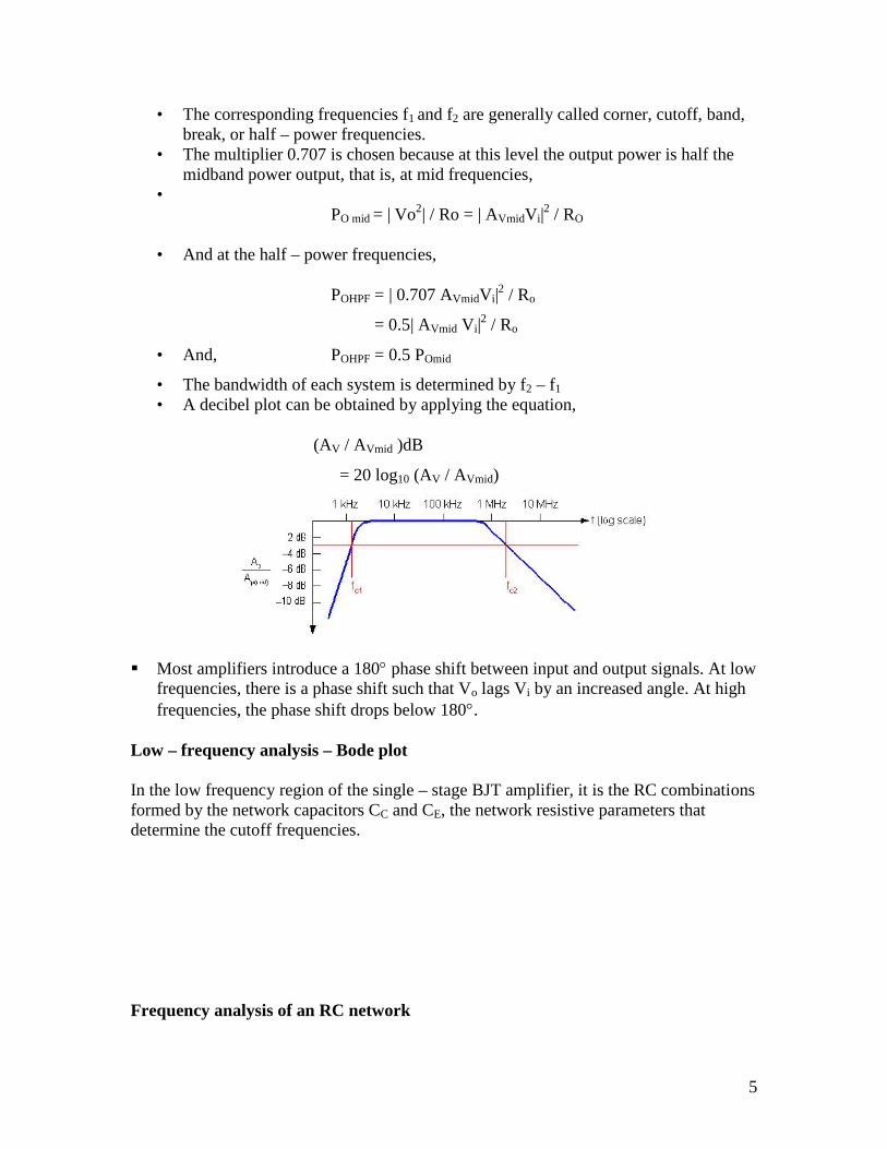
• In the frequency response, there is a band of frequencies in which the magnitudeof the gain is either equal or relatively close to the midband value.
• To fix the frequency boundaries of relatively high gain, 0.707AVmid is chosen tobe the gain at the cutoff levels.
5
• The corresponding frequencies f1 and f2 are generally called corner, cutoff, band,break, or half – power frequencies.
• The multiplier 0.707 is chosen because at this level the output power is half themidband power output, that is, at mid frequencies,
•PO mid = | Vo2| / Ro = | AVmidVi|
2 / RO
• And at the half – power frequencies,
POHPF = | 0.707 AVmidVi|2 / Ro
= 0.5| AVmid Vi|2 / Ro
• And, POHPF = 0.5 POmid
• The bandwidth of each system is determined by f2 – f1
• A decibel plot can be obtained by applying the equation,
(AV / AVmid )dB
= 20 log10 (AV / AVmid)
Most amplifiers introduce a 180 phase shift between input and output signals. At lowfrequencies, there is a phase shift such that Vo lags Vi by an increased angle. At highfrequencies, the phase shift drops below 180.
Low – frequency analysis – Bode plot
In the low frequency region of the single – stage BJT amplifier, it is the RC combinationsformed by the network capacitors CC and CE, the network resistive parameters thatdetermine the cutoff frequencies.
Frequency analysis of an RC network

6
• Analysis of the above circuit indicates that,
XC = 1/2fC 0
• Thus, Vo = Vi at high frequencies.
• At f = 0 Hz, XC = , Vo = 0V.
• Between the two extremes, the ratio, AV = Vo / Vi will vary.As frequency increases, the capacitive reactance decreases and more of the inputvoltage appears across the output terminals.
The output and input voltages are related by the voltage – divider rule:
Vo = RVi / ( R – jXC)
the magnitude of Vo = RVi / R2 + XC2
• For the special case where XC = R,
Vo =RVi / R2 = (1/2) Vi
AV = Vo / Vi = (1/2) = 0.707
• The frequency at which this occurs is determined from,
XC = 1/2f1C = R
where, f1 = 1/ 2RC
• Gain equation is written as,
AV = Vo / Vi
= R / (R – jXC) = 1/ ( 1 – j(1/CR)
= 1 / [ 1 – j(f1 / f)]
• In the magnitude and phase form,
AV = Vo / Vi
= [1 / 1 + (f1/f)2 ] tan-1 (f1 / f)
• In the logarithmic form, the gain in dB is
7
AV = Vo / Vi = [1 / 1 + (f1/f)2 ]
= 20 log 10 [1 / 1 + (f1/f)2 ]
= - 20 log 10 [ 1 + (f1/f)2]
= - 10 log10 [1 + (f1/f)2]
• For frequencies where f << f1 or (f1/ f)2 the equation can be approximated by
AV (dB) = - 10 log10 [ (f1 / f)2]
= - 20 log10 [ (f1 / f)] at f << f1
• At f = f1 ;
f1 / f = 1 and
– 20 log101 = 0 dB
• At f = ½ f1;
f1 / f = 2
– 20 log102 = - 6 dB
• At f = ¼ f1;
f1 / f = 4
– 20 log102 = - 12 dB
• At f = 1/10 f1;
f1 / f = 10
– 20 log1010 = - 20dB
• The above points can be plotted which forms the Bode – plot.
• Note that, these results in a straight line when plotted in a logarithmic scale.Although the above calculation shows at f = f1, gain is 3dB, we know that f1 isthat frequency at which the gain falls by 3dB. Taking this point, the plot differsfrom the straight line and gradually approaches to 0dB by f = 10f1.
Observations from the above calculations:
• When there is an octave change in frequency from f1 / 2 to f1, there existscorresponding change in gain by 6dB.
• When there is an decade change in frequency from f1 / 10 to f1, there existscorresponding change in gain by 20 dB.
8
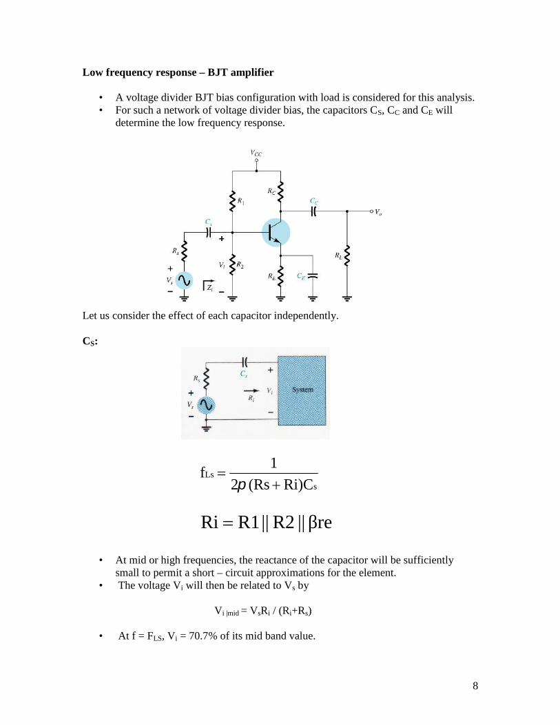
Low frequency response – BJT amplifier
• A voltage divider BJT bias configuration with load is considered for this analysis.• For such a network of voltage divider bias, the capacitors CS, CC and CE will
determine the low frequency response.
Let us consider the effect of each capacitor independently.
CS:
• At mid or high frequencies, the reactance of the capacitor will be sufficientlysmall to permit a short – circuit approximations for the element.
• The voltage Vi will then be related to Vs by
Vi |mid = VsRi / (Ri+Rs)
• At f = FLS, Vi = 70.7% of its mid band value.
sLs
Ri)C(Rs2
1f
βre||R2||R1Ri

9
• The voltage Vi applied to the input of the active device can be calculated using thevoltage divider rule:
Vi = RiVs / ( Ri+ Rs – jXCs)Effect of CC:
• Since the coupling capacitor is normally connected between the output of theactive device and applied load, the RC configuration that determines the lowcutoff frequency due to CC appears as in the figure given below.
•
• Ro = Rc|| ro
Effect of CE:
)CcRRo(π2
1f
LLC
EeLE
CRπ2
1f )r
βsR
(||RR eEe
R2||R1||RssR

10
• The effect of CE on the gain is best described in a quantitative manner by recallingthat the gain for the amplifier without bypassing the emitter resistor is given by:
AV = - RC / ( re + RE)• Maximum gain is obviously available where RE is 0.• At low frequencies, with the bypass capacitor CE in its “open circuit” equivalent
state, all of RE appears in the gain equation above, resulting in minimum gain.• As the frequency increases, the reactance of the capacitor CE will decrease,
reducing the parallel impedance of RE and CE until the resistor RE is effectivelyshorted out by CE.
• The result is a maximum or midband gain determined by AV = - RC / re.• The input and output coupling capacitors, emitter bypass capacitor will affect only
the low frequency response.• At the mid band frequency level, the short circuit equivalents for these capacitors
can be inserted.• Although each will affect the gain in a similar frequency range, the highest low
frequency cutoff determined by each of the three capacitors will have the greatestimpact.
Problem:
Determine the lower cutoff freq. for the network shown using the followingparameters:
Cs = 10μF, CE = 20μF, Cc = 1μF
Rs = 1kΩ, R1= 40kΩ, R2 = 10kΩ,
RE = 2kΩ, RC = 4kΩ, RL = 2.2kΩ,
β = 100, ro = ∞Ω, Vcc = 20V
• Solution:

11
a. To determine re for the dc conditions, let us check whether RE > 10R2
Here, RE = 200k, 10R2 = 100k. The condition is satisfied. Thus approximate
analysis can be carried out to find IE and thus re.
VB = R2VCC / ( R1+R2) = 4V
VE = VB – 0.7 = 3.3V
IE = 3.3V / 2k = 1.65mA
re = 26mV / 1.65mA = 15.76
Mid band gain:
AV = Vo / Vi = -RC||RL / re = - 90
• Input impedance
Zi = R1 || R2|| re = 1.32K
• Cut off frequency due to input coupling capacitor ( fLs)
fLs = 1/ [2(Rs +Ri)CC1 = 6.86Hz.
fLc = 1 / [2(RC + RL) CC
= 1 / [ 6.28 (4k + 2.2k)1uF]
= 25.68 Hz
Effect of CE:
RS = RS||R1||R2 = 0.889
Re = RE || (RS/ + re) = 24.35
fLe = 1/2 ReCE = 327 Hz
fLe = 327 Hz
fLC = 25.68Hz
fLs = 6.86Hz
In this case, fLe is the lower cutoff frequency.
• In the high frequency region, the capacitive elements of importance are the inter-electrode ( between terminals) capacitances internal to the active device and thewiring capacitance between leads of the network.
• The large capacitors of the network that controlled the low frequency response areall replaced by their short circuit equivalent due to their very low reactance level.
• For inverting amplifiers, the input and output capacitance is increased by acapacitance level sensitive to the inter-electrode capacitance between the inputand output terminals of the device and the gain of the amplifier.
12
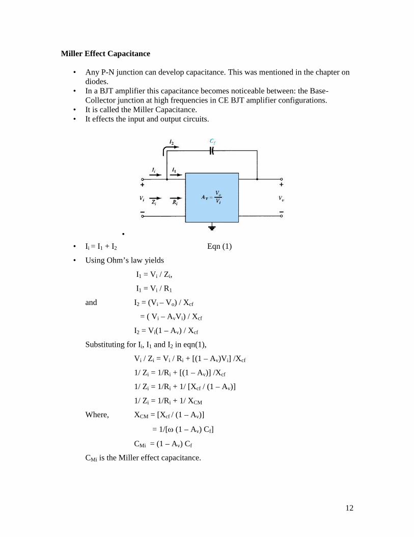
Miller Effect Capacitance
• Any P-N junction can develop capacitance. This was mentioned in the chapter ondiodes.
• In a BJT amplifier this capacitance becomes noticeable between: the Base-Collector junction at high frequencies in CE BJT amplifier configurations.
• It is called the Miller Capacitance.• It effects the input and output circuits.
•• Ii = I1 + I2 Eqn (1)
• Using Ohm’s law yields
I1 = Vi / Zi,
I1 = Vi / R1
and I2 = (Vi – Vo) / Xcf
= ( Vi – AvVi) / Xcf
I2 = Vi(1 – Av) / Xcf
Substituting for Ii, I1 and I2 in eqn(1),
Vi / Zi = Vi / Ri + [(1 – Av)Vi] /Xcf
1/ Zi = 1/Ri + [(1 – Av)] /Xcf
1/ Zi = 1/Ri + 1/ [Xcf / (1 – Av)]
1/ Zi = 1/Ri + 1/ XCM
Where, XCM = [Xcf / (1 – Av)]
= 1/[ (1 – Av) Cf]
CMi = (1 – Av) Cf
CMi is the Miller effect capacitance.

13
• For any inverting amplifier, the input capacitance will be increased by a Millereffect capacitance sensitive to the gain of the amplifier and the inter-electrode( parasitic) capacitance between the input and output terminals of the activedevice.
Miller Output Capacitance (CMo)
Applying KCL at the output node results in:
Io = I1+I2
I1 = Vo/Ro
and I2 = (Vo – Vi) / XCf
The resistance Ro is usually sufficiently large to permit ignoring the first term of theequation, thus
Io (Vo – Vi) / XCf
Substituting Vi = Vo / AV,
Io = (Vo – Vo/Av) / XCf
= Vo ( 1 – 1/AV) / XCf
Io / Vo = (1 – 1/AV) / XCf
Vo / Io = XCf / (1 – 1/AV)
= 1 / Cf (1 – 1/AV)
= 1/ CMo
CMo = ( 1 – 1/AV)Cf
fMo CC
14
CMo Cf [ |AV| >>1]
If the gain (Av) is considerably greater than 1:
High frequency response – BJT Amplifier
• At the high – frequency end, there are two factors that define the – 3dB cutoff point:– The network capacitance ( parasitic and introduced) and– the frequency dependence of hfe()
Network parameters
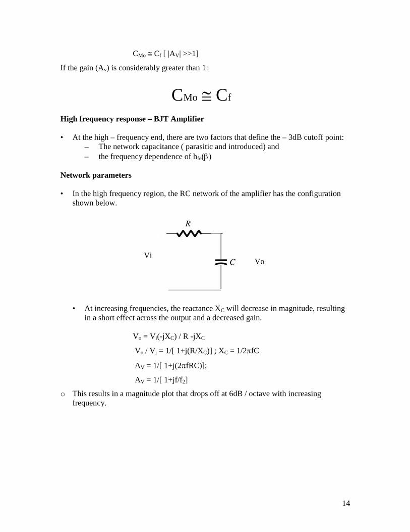
• In the high frequency region, the RC network of the amplifier has the configurationshown below.
• At increasing frequencies, the reactance XC will decrease in magnitude, resultingin a short effect across the output and a decreased gain.
Vo = Vi(-jXC) / R -jXC
Vo / Vi = 1/[ 1+j(R/XC)] ; XC = 1/2fC
AV = 1/[ 1+j(2fRC)];
AV = 1/[ 1+jf/f2]
o This results in a magnitude plot that drops off at 6dB / octave with increasingfrequency.
fMo CC
ViVo
15
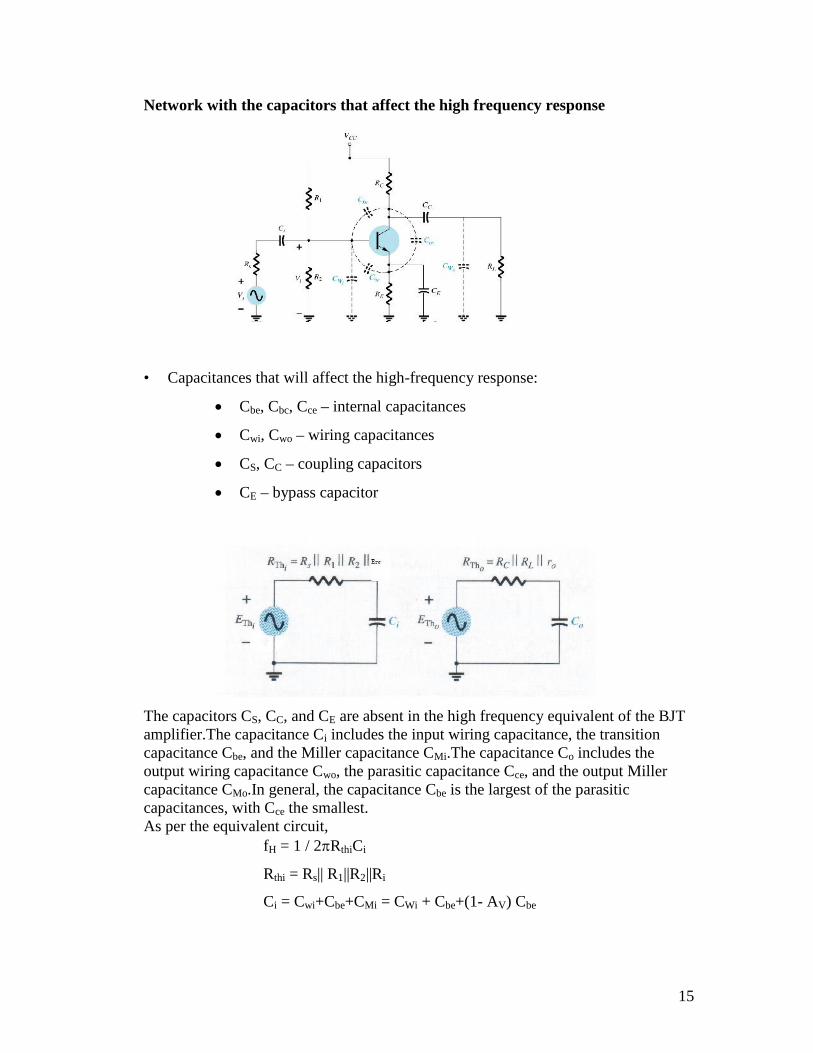
Network with the capacitors that affect the high frequency response
• Capacitances that will affect the high-frequency response:
Cbe, Cbc, Cce – internal capacitances
Cwi, Cwo – wiring capacitances
CS, CC – coupling capacitors
CE – bypass capacitor
The capacitors CS, CC, and CE are absent in the high frequency equivalent of the BJTamplifier.The capacitance Ci includes the input wiring capacitance, the transitioncapacitance Cbe, and the Miller capacitance CMi.The capacitance Co includes theoutput wiring capacitance Cwo, the parasitic capacitance Cce, and the output Millercapacitance CMo.In general, the capacitance Cbe is the largest of the parasiticcapacitances, with Cce the smallest.As per the equivalent circuit,
fH = 1 / 2RthiCi
Rthi = Rs|| R1||R2||Ri
Ci = Cwi+Cbe+CMi = CWi + Cbe+(1- AV) Cbe
16
At very high frequencies, the effect of Ci is to reduce the total impedance of theparallel combination of R1, R2, Ri, and Ci.The result is a reduced level of voltageacross Ci, a reduction in Ib and the gain of the system.For the output network,
fHo = 1/(2RThoCo)
RTho = RC||RL||ro
Co = Cwo+Cce+CMo
At very high frequencies, the capacitive reactance of Co will decrease andconsequently reduce the total impedance of the output parallel branches.The net result is that Vo will also decline toward zero as the reactance Xc becomessmaller.The frequencies fHi and fHo will each define a -6dB/octave asymtote.If the parasitic capacitors were the only elements to determine the high – cutofffrequency, the lowest frequency would be the determining factor.However, thedecrease in hfe(or ) with frequency must also be considered as to whether its breakfrequency is lower than fHi or fHo.
hfe (or ) variation
• The variation of hfe( or ) with frequency will approach the following relationship
hfe = hfe mid / [1+(f/f)]
• f is that frequency at which hfe of the transistor falls by 3dB with respect to itsmid band value.
• The quantity f is determined by a set of parameters employed in the hybrid model.
• In the hybrid model, rb includes the• base contact resistance
• base bulk resistance
• base spreading resistance

17
Hybrid model
• The resistance ru(rbc) is a result of the fact that the base current is somewhatsensitive to the collector – to – base voltage.
• Since the base – to – emitter voltage is linearly related to the base current throughOhm’s law and the output voltage is equal to the difference between the base thebase – to – emitter voltage and collector – to – base voltage, we can say that thebase current is sensitive to the changes in output voltage.
• Thus,
f = 1/[2r(C+Cu)]
r = re = hfe mid re
• Therefore,
f = 1/[2 hfemid re(C+Cu)]
OR
f = 1/[2 mid re(C+Cu)]
• The above equation shows that, f is a function of the bias configuration.
• As the frequency of operation increases, hfe will drop off from its mid band valuewith a 6dB / octave slope.
• Common base configuration displays improved high frequency characteristicsover the common – emitter configuration.
• Miller effect capacitance is absent in the Common base configuration due to noninverting characteristics.
• A quantity called the gain – bandwidth product is defined for the transistor by thecondition,
| hfemid / [1+j(f/f)| = 1
• So that,
|hfe|dB = 20 log10 | hfemid / [1+j(f/f)|
= 20 log101 = 0 dB
• The frequency at which |hfe|dB = 0 dB is indicated by fT.

18
| hfemid / [1+j(f/f)| = 1
hfemid / 1+ (fT/f)2 hfemid / (fT/f) =1
( by considering fT>>f)
• Thus, fT = hfemid f OR fT = mid f
• But, f = 1/[2 mid re(C+Cu)]
fT = (mid) 1/[2 mid re(C+Cu)]
fT = 1/[2 re(C+Cu)]
Problem:
For the amplifier with voltage divider bias, the following parameters are given:
RS = 1k , R1 = 40k, R2 = 10k, Rc = 4k, RL = 10k
Cs = 10F, Cc = 1 F, CE= 20 F
= 100, ro = , VCC = 10
C = 36pF, Cu = 4pF, Cce=1pF, Cwi=6pF, Cwo=8pF
a. Determine fHi and fHo
b. Find f and fT
Solution:
To find re, DC analysis has to be performed to find IE.
VB = R2VCC / R1+R2 = 2V
VE = 2 – 0.7 = 1.3V
IE = 1.3/1.2K = 1.083mA
re = 26mV / 1.083mA
re = 24.01,
re = 2.4k
Ri = RS||R1||R2||re
Ri = 1.85k
AV = Vo/Vi = - (Rc ||RL) / re
AV = - 119
RThi = Rs||R1||R2||Ri
19
RThi = 0.6k
To determine fHi and fHo:
fHi = 1/[2RThiCi] ;
Ci = Cwi+Cbe+(1 – AV)Cbc
= 6pF + 36pF + (1 – (-119)) 4pF
Ci = 522pF
fHi = 1/2RThiCi
fHi = 508.16kHz
RTho = Rc||RL
RTho = 2.86k
Co = Cwo+Cce+C Mo
= 8pF+1pF+(1 – (1/-119))4pF
Co = 13.03pF
fHo = 1/2RThoCo
fHo = 8.542MHz
f = 1/[2 mid re(C+Cu)]
f = 1.66MHz
fT = f
fT = 165.72MHz
Summary – Frequency response of BJT Amplifiers
• Logarithm of a number gives the power to which the base must be brought toobtain the same number
• Since the decibel rating of any equipment is a comparison between levels, areference level must be selected for each area of application.
• For Audio system, reference level is 1mW• The dB gain of a cascaded systems is the sum of dB gains of each stage.• It is the capacitive elements of a network that determine the bandwidth of a
system.• The larger capacitive elements of the design determine the lower cutoff
frequencies.• Smaller parasitic capacitors determine the high cutoff frequencies.• The frequencies at which the gain drops to 70.7% of the mid band value are called
– cutoff, corner, band, break or half power frequencies.• The narrower the bandwidth, the smaller is the range of frequencies that will
permit a transfer of power to the load that is atleast 50% of the midband level.

20
• A change in frequency by a factor of 2, is equivalent to one octave which resultsin a 6dB change in gain.
• For a 10:1 change in frequency is equivalent to one decade results in a 20dBchange in gain.
• For any inverting amplifier, the input capacitance will be increased by a Millereffect capacitance determined by the gain of the amplifier and the inter electrode( parasitic) capacitance between the input and output terminals of the activedevice.
CMi = (1 – AV)Cf
• Also, CMo Cf (if AV >>1)
• A 3dB drop in will occur at a frequency defined by f, that is sensitive to the DCoperating conditions of the transistor.
• This variation in defines the upper cutoff frequency of the design.
Problems:
1. The total decibel gain of a 3 stage system is 120dB. Determine the dB gain ofeach stage, if the second stage has twice the decibel gain of the first and the thirdhas 2.7 times decibel gain of the first. Also, determine the voltage gain of the eachstage.
• Given: GdBT = 120dB
We have GdBT = GdB1+GdB2+GdB3
Given, GdB2 = 2GdB1
GdB3 = 2.7GdB1
Therefore, 120dB = 5.7GdB1
GdB1 = 21.05,
GdB2 = 42.10
GdB3 =56.84
We have GdB = 10 log[Vo / Vi]
Vo / Vi = antilog ( GdB/10)
G1 = 127.35
G2 = 16.21k
G3 = 483.05k
2. If the applied ac power to a system is 5W at 100mV and the output power is 48W,determine
a. The power gain in decibels

21
b. The output voltagec. The voltage gain in decibels, if the output impedance is 40k.d. The input impedance
Given: Pi = 5W.Vi = 100mV, Po = 48w Ro = 40k
a. GdB =10 log [48/ 5] = 69.82
b. Po = Vo2 /Ro,
Vo = PoRo = 1385.64V
c. Voltage gain in dB = 20 log [1385.64/100m] = 82.83
d. Ri = Vi2 / Pi = 2k
General steps to solve a given problem:
Normally, the amplifier circuit with all the values of biasing resistors, value of andvalues inter electrode capacitances ( Cbe, Cbc and Cce) will be given.It is required to calculate: fLS, fLC and fLE
Also, fHi, fHo, f and fT
• Step1: Perform DC analysis and find the value of IE, and re
– Find the value of Ri ( Zi) using the value of re
– Find the value of AVmid
• Step 2: Find fLS using the formula 1/2(Ri+RS)CS
• Step 3: Find fLC using the formula 1/2(RC+RL)CC
• Step 4: Determine the value of fLE using the formula 1/2ReCE
where, Re = RE || [(RS)/ + re]
RS = RS||R1||R2
• Step 5: Determine fHi using the formula 1/2RThiCi
where RThi = R1||R2||RS||re
Ci = Cwi + Cbe + (1-AV)Cbc
• Step 6: Determine fHo using the formula 1/2RThoCo
where RTho = RC||RL||ro
Co = Cwo + Cce+ C bc
• Step 7: Determine f using the formula 1/[2 mid re(C+Cu)]
22
• Step 8: Determine fT using the formula fT = mid f
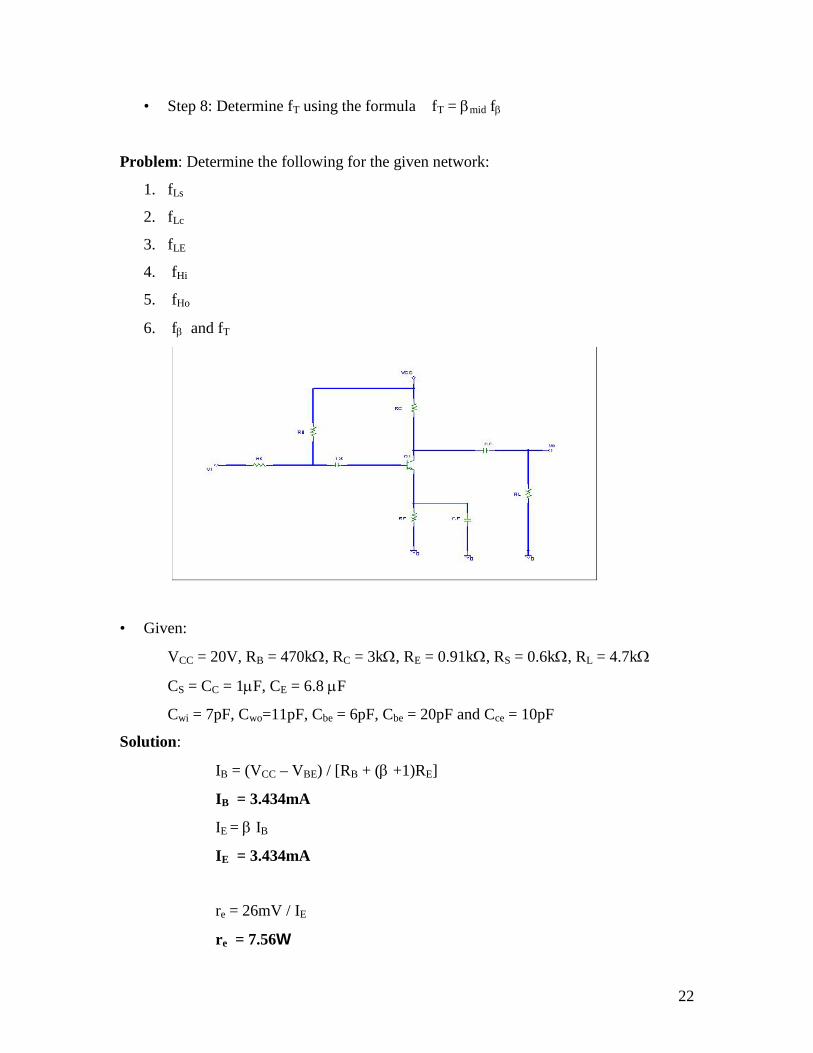
Problem: Determine the following for the given network:
1. fLs
2. fLc
3. fLE
4. fHi
5. fHo
6. f and fT
• Given:
VCC = 20V, RB = 470k, RC = 3k, RE = 0.91k, RS = 0.6k, RL = 4.7k
CS = CC = 1F, CE = 6.8 F
Cwi = 7pF, Cwo=11pF, Cbe = 6pF, Cbe = 20pF and Cce = 10pF
Solution:
IB = (VCC – VBE) / [RB + ( +1)RE]
IB = 3.434mA
IE = IB
IE = 3.434mA
re = 26mV / IE
re = 7.56

23
AV = - (RC||RL) / re
AV = -242.2
Zi = RB|| re
Zi = 754.78
fLS = 1/2(Ri+RS)CS
fLS = 117.47Hz
fLC = 1/2(RC+RL)CC
fLC = 20.66 Hz
fLE = 1/2ReCE ;
where, Re = [(RS /)+ re] || RE
RS = RB || RS
fLE = 1.752kHz
Ci = Cwi + Cbe + (1 – AV) Cbc
Ci = 1.48nF
RThi = RS || RB|| re
RThi = 334.27
fHi = 1 / 2(1.48nF)(334.37)
fHi = 321.70 KHz
Co = CWo + Cce + (1 – 1/AV) Cbc
Co = 27.02pF
RTho = RC || RL
RTho = 1.83K
fHo = 1 / 2(27.02p)(1.83k)
fHo = 3.21MHz
f = 1 / 2 (100) (7.56)( 20p + 6p)
f = 8.09MHz
fT = f
fT = 803MHz

24
Equations - Logarithms
1. a = bx, x = logba
2. GdB = 10 log P2 / P1
3. GdB = 20 log V2 / V1
Equations – Low frequency response
1. AV = 1 / [1 – j(f1/f)],
where, f1 = 1/2RC
Equations – BJT low frequency response
1. fLs = 1 / [2(RS+Ri)CS] ,
where, Ri = R1||R2||re
2. fLC = 1 /[2(Ro+RL)CC],
where, Ro = RC||ro
3. fLE = 1 / 2ReCE,
where, Re = RE || ( RS/ +re) and RS = RS||R1||R2
Miller effect Capacitance
CMi = (1 – AV)Cf,
CMO = ( 1 – 1/AV)Cf
BJT High frequency response:
1. AV = 1/ [1 + j(f/f2)]
2. fHi = 1 / 2RThiCi,
where, RThi = RS||R1||R2||Ri, Ci = CWi+Cbe+ CMi
3. fHO = 1/ 2RThoCo,
where, RTho = RC||RL||ro
Co = CWo+Cce+ CMo
4. f = 1/[2 mid re(C+Cu)]
5. fT = f