Embed Size (px)
Citation preview
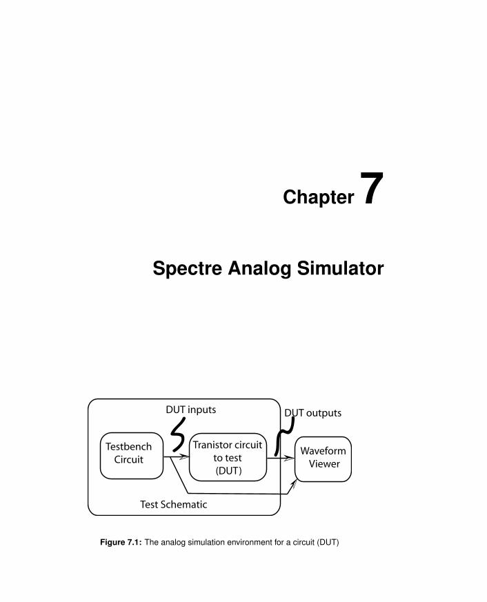
Chapter 7
Spectre Analog Simulator
Tranistor circuitto test (DUT)
Test Schematic
Waveform Viewer
DUT inputs DUT outputs
TestbenchCircuit
Figure 7.1: The analog simulation environment for a circuit (DUT)
106 CHAPTER 7: Spectre Analog Simulator
(Copyright c©2005, 2010, Cadence Design Systems, Inc. All rights reserved worldwide. Reprinted with permission.)
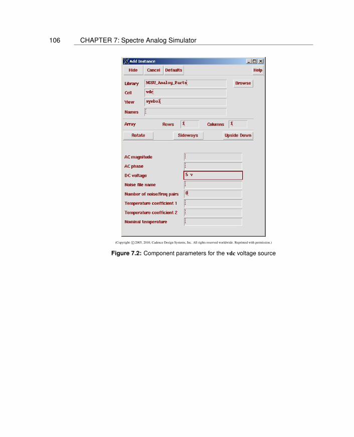
Figure 7.2: Component parameters for the vdc voltage source

107
(Copyright c©2005, 2010, Cadence Design Systems, Inc. All rights reserved worldwide. Reprinted with permission.)
Figure 7.3: Component parameters for the vpulse voltage source

108 CHAPTER 7: Spectre Analog Simulator
(Copyright c©2005, 2010, Cadence Design Systems, Inc. All rights reserved worldwide. Reprinted with permission.)
Figure 7.4: Schematic for the nand-test DUT/testbench circuit

109
(Copyright c©2005, 2010, Cadence Design Systems, Inc. All rights reserved worldwide. Reprinted with permission.)
Figure 7.5: Virtuoso Analog Environment control window
(Copyright c©2005, 2010, Cadence Design Systems, Inc. All rights reserved worldwide. Reprinted with permission.)
Figure 7.6: Choosing Analyses dialog box

110 CHAPTER 7: Spectre Analog Simulator
(Copyright c©2005, 2010, Cadence Design Systems, Inc. All rights reserved worldwide. Reprinted with permission.)
Figure 7.7: Spectre log window for the NAND simulation

111
(Copyright c©2005, 2010, Cadence Design Systems, Inc. All rights reserved worldwide. Reprinted with permission.)
Figure 7.8: Initial waveform output window

112 CHAPTER 7: Spectre Analog Simulator
(Copyright c©2005, 2010, Cadence Design Systems, Inc. All rights reserved worldwide. Reprinted with permission.)
Figure 7.9: Waveform output window in strip mode

113
(Copyright c©2005, 2010, Cadence Design Systems, Inc. All rights reserved worldwide. Reprinted with permission.)
Figure 7.10: Waveform output window: zoomed view
114 CHAPTER 7: Spectre Analog Simulator
(Copyright c©2005, 2010, Cadence Design Systems, Inc. All rights reserved worldwide. Reprinted with permission.)
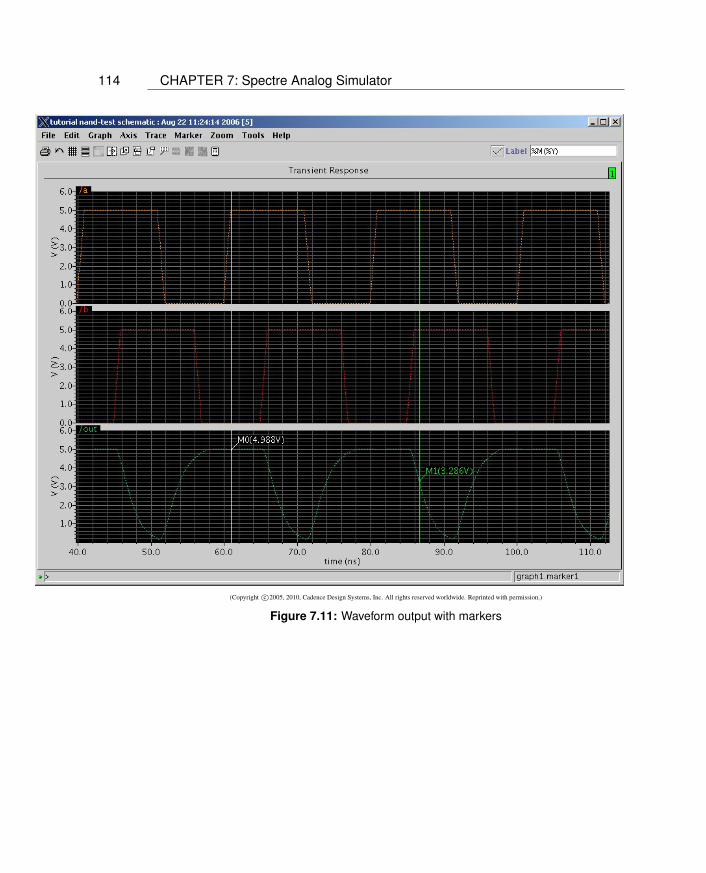
Figure 7.11: Waveform output with markers
115
(Copyright c©2005, 2010, Cadence Design Systems, Inc. All rights reserved worldwide. Reprinted with permission.)
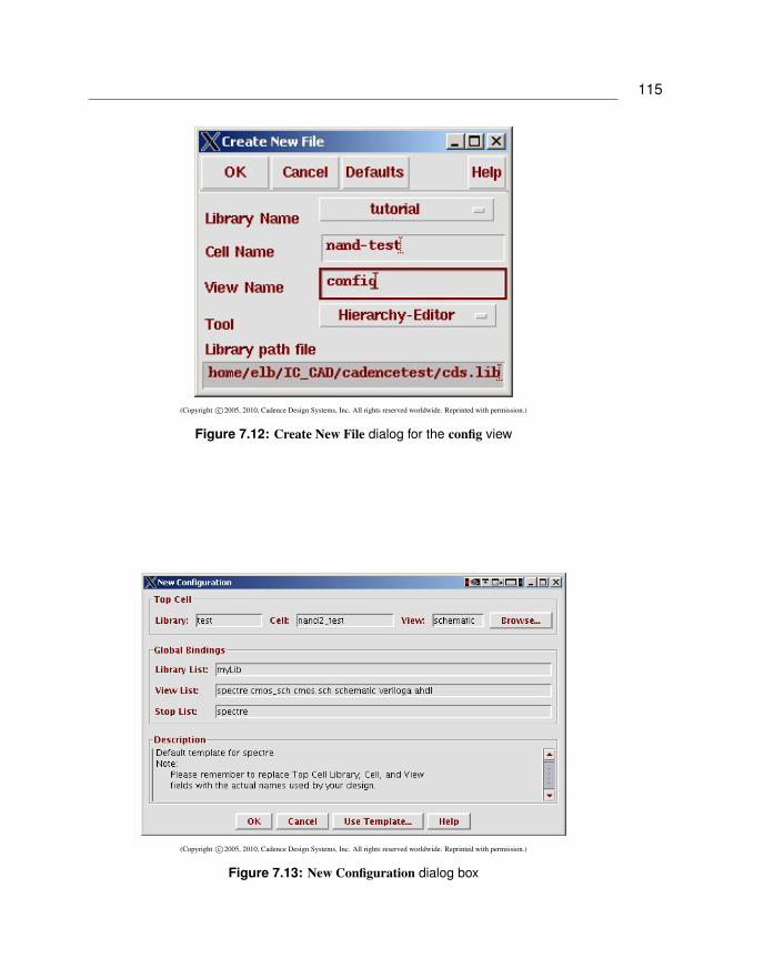
Figure 7.12: Create New File dialog for the config view
(Copyright c©2005, 2010, Cadence Design Systems, Inc. All rights reserved worldwide. Reprinted with permission.)
Figure 7.13: New Configuration dialog box

116 CHAPTER 7: Spectre Analog Simulator
(Copyright c©2005, 2010, Cadence Design Systems, Inc. All rights reserved worldwide. Reprinted with permission.)
Figure 7.14: Hierarchy Editor view for nand-test (table view)

117
(Copyright c©2005, 2010, Cadence Design Systems, Inc. All rights reserved worldwide. Reprinted with permission.)
Figure 7.15: Hierarchy Editor view for nand-test (tree view)

118 CHAPTER 7: Spectre Analog Simulator
(Copyright c©2005, 2010, Cadence Design Systems, Inc. All rights reserved worldwide. Reprinted with permission.)
Figure 7.16: Test schematic for the mixed-mode NAND (DUT) simulation

119
(Copyright c©2005, 2010, Cadence Design Systems, Inc. All rights reserved worldwide. Reprinted with permission.)
Figure 7.17: Mixed-mode config view for mixed-nand

120 CHAPTER 7: Spectre Analog Simulator
(Copyright c©2005, 2010, Cadence Design Systems, Inc. All rights reserved worldwide. Reprinted with permission.)
Figure 7.18: Interface library dialog box
(Copyright c©2005, 2010, Cadence Design Systems, Inc. All rights reserved worldwide. Reprinted with permission.)
Figure 7.19: d2a interface element parameters

121
(Copyright c©2005, 2010, Cadence Design Systems, Inc. All rights reserved worldwide. Reprinted with permission.)
Figure 7.20: a2d interface element parameters

122 CHAPTER 7: Spectre Analog Simulator
(Copyright c©2005, 2010, Cadence Design Systems, Inc. All rights reserved worldwide. Reprinted with permission.)
Figure 7.21: Mixed-mode config view with analog/Verilog partitioning

123
(Copyright c©2005, 2010, Cadence Design Systems, Inc. All rights reserved worldwide. Reprinted with permission.)
Figure 7.22: The mixed-test schematic showing analog/digital partitioning

124 CHAPTER 7: Spectre Analog Simulator
// Verimix stimulus file.// Default verimix stimulus.
initialbegin
a = 1’b0;b = 1’b0;
#10 $display("ab = %b%b, out = %b", a, b, dout);if (dout != 1) $display("Error - that’s wrong!");
a=1;#10 $display("ab = %b%b, out = %b", a, b, dout);if (dout != 1) $display("Error - that’s wrong!");
b=1;#10 $display("ab = %b%b, out = %b", a, b, dout);if (dout != 0) $display("Error - that’s wrong!");
a=0;#10 $display("ab = %b%b, out = %b", a, b, dout);if (dout != 1) $display("Error - that’s wrong!");
end
Figure 7.23: The digital testbench for the mixed-nand simulation

125
(Copyright c©2005, 2010, Cadence Design Systems, Inc. All rights reserved worldwide. Reprinted with permission.)
Figure 7.24: Results of the mixed-mode simulation of mixed-test

126 CHAPTER 7: Spectre Analog Simulator
(Copyright c©2005, 2010, Cadence Design Systems, Inc. All rights reserved worldwide. Reprinted with permission.)
Figure 7.25: Rearranged results of the mixed-mode simulation

127
Switching from DC to transient.VERILOG time 0 (units of 100ps) corresponds to spectre time 0.
Message! At the end of DC initialization the logic valuesof the following ports are X (unknown):
net16net18
[Mixed_Sig]"IE.verimix", 4: ...
ab = 00, out = 1ab = 10, out = 1ab = 11, out = 0ab = 01, out = 1Verilog/spectre Interface: 165 messages sent, 167 messages received.0 simulation events(use +profile or +listcounts option to count) + 29 accelerated eventsCPU time: 0.0 secs to compile + 0.0 secs to link + 3.6 secs in simulationEnd of Tool: VERILOG-XL 05.81.001-p Aug 23, 2006 10:58:39
Figure 7.26: $display output from the mixed-test simulation
// Verimix stimulus file.// Default verimix stimulus.
integer file; // declare the file descriptor firstinitialbegin
file = $fopen("/home/elb/IC_CAD/cadencetest/testout.txt");a = 1’b0;b = 1’b0;
$fdisplay(file, "Starting mixed-test simulation of NAND");$fdisplay(file, "using digital inputs to an analog simulation");
#10 $fdisplay(file, "ab = %b%b, out = %b", a, b, dout);if (dout != 1) $fdisplay(file, "Error - that’s wrong!");
a=1;#10 $fdisplay(file, "ab = %b%b, out = %b", a, b, dout);if (dout != 1) $fdisplay(file, "Error - that’s wrong!");
b=1;#10 $fdisplay(file, "ab = %b%b, out = %b", a, b, dout);if (dout != 0) $fdisplay(file, "Error - that’s wrong!");
a=0;#10 $fdisplay(file, "ab = %b%b, out = %b", a, b, dout);if (dout != 1) $fdisplay(file, "Error - that’s wrong!");
end
Figure 7.27: mixed-test testbench file with file I/O

128 CHAPTER 7: Spectre Analog Simulator
Starting mixed-test simulation of NANDusing digital inputs to an analog simulationab = 00, out = 1ab = 10, out = 1ab = 11, out = 0ab = 01, out = 1
Figure 7.28: mixed-test testbench file with file I/O
Figure 7.29: Simple circuit for DC analysis (schematic view)

129
(Copyright c©2005, 2010, Cadence Design Systems, Inc. All rights reserved worldwide. Reprinted with permission.)
Figure 7.30: Component parameter selection dialog box for DC analysis

130 CHAPTER 7: Spectre Analog Simulator
(Copyright c©2005, 2010, Cadence Design Systems, Inc. All rights reserved worldwide. Reprinted with permission.)
Figure 7.31: DC analysis dialog box

131
(Copyright c©2005, 2010, Cadence Design Systems, Inc. All rights reserved worldwide. Reprinted with permission.)
Figure 7.32: Analog Environment dialog box for DC analysis

132 CHAPTER 7: Spectre Analog Simulator
(Copyright c©2005, 2010, Cadence Design Systems, Inc. All rights reserved worldwide. Reprinted with permission.)
Figure 7.33: DC analysis output waveform for a single set of parameters

133
(Copyright c©2005, 2010, Cadence Design Systems, Inc. All rights reserved worldwide. Reprinted with permission.)
Figure 7.34: Dialog to set variable parameters for parametric simulation

134 CHAPTER 7: Spectre Analog Simulator
(Copyright c©2005, 2010, Cadence Design Systems, Inc. All rights reserved worldwide. Reprinted with permission.)
Figure 7.35: Output of parametric DC simulation with five curves

135
Figure 7.36: Test schematic for power measurements of a NAND gate

136 CHAPTER 7: Spectre Analog Simulator
Figure 7.37: Analog simulation output from NAND gate simulation using Spectre
137
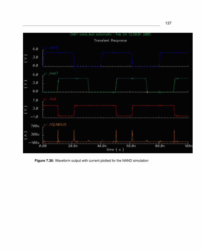
Figure 7.38: Waveform output with current plotted for the NAND simulation

138 CHAPTER 7: Spectre Analog Simulator
(Copyright c©2005, 2010, Cadence Design Systems, Inc. All rights reserved worldwide. Reprinted with permission.)
Figure 7.39: Dialog box for the Spectre Analog Environment calculator