Embed Size (px)
Citation preview
ISSUE NO. 34 VOL. XXXIV THE INDIAN INSTITUTE OF METALS 26-06-2010 3
Chapter NewsExecutive Committee MeetingThe first E C Meeting of the year 2010-11 was held on 29th May 2010 in the office of IIM DelhiChapter. The name of Shri L Pugazhenthy and Mr. J. Mazumdar were decided for the advisorycommittee to the EC. The name of the third member is yet to be decided.
The technical and publication committee was formed under the chairmanship of Shri S C Suriwith S/Shri G. I. S. Chauha, R. K. Vijayvargia, D. K. Likhi, Dr. A. K. Srivastava, Neeraj Gupta,Manoranjan Ram and Dr. (Mrs.) Malti Goel as memebrs of this committee. The formation ofvarious other committess is in progress.
Various suggestions were received and deliberated by members such as more technicalactivities, plant visits and technical talks. It was also suggested that Delhi Chapter may inviteneighbourhood chapters for parcipating in such activities.
Metallurgical Principles in Secondary Steel MakingS C Suri
Life Fellow, IIM & ChairmanTechnical & Publication Committee
1.0 IntroductionSteel quality demands are becoming increasingly stringent. These demands are beyondthe normal steel making operations. This requirement is true for specialty steel products.This has resulted in the advent of various secondary steel making processes.
Primary steel making is employed in the steel making furnace. Further refining and controland alloy additions are undertaken in the secondary steel making processes.
The paper reviews the principles of various secondary steel making processes beingemployed for production of specialty steels which require very stringent qualityparameters.
2.0 Secondary Steel Making ProcessesHistorically Vacuum Degassing (VD) process came in the decades of 1950-60. The initialobjective was to lower hydrogen content of liquid steel in order to prevent cracks in largeforging quality ingots. Later on the objective also included lowering of nitrogen andoxygen contents.
Purging with inert gas (Argon or Nitrogen) in the ladle using porus plug camesubsequently. Its primary objective was stirring with consequent homogenization oftemperature and composition of the melt. It offered the advantage of floating of oxideinclusions resulting in cleaner steels.
It is possible to lower carbon content to a very low value in stainless steel by treatment ofthe melt with oxygen under vacuum or along with Argon stream.
This led to development of process such as vacuum oxygen decarburization (VOD) andArgon Oxygen Decarburization (AOD).
Synthetic slag treatment and powder injection process of molten steel in ladle werestarted in late 60’s and early 70’s with the objective of controlling sulphur content of steel
ISSUE NO. 34 VOL. XXXIV THE INDIAN INSTITUTE OF METALS 26-06-2010 4
to a low level that are demanded for many applications.
This led to the development of what is known as Injection Metallurgy. Injection of powdersof calcium bearing reagents typically calcium silicide was also found to prevent nozzleclogging by Al2O3.
In traditional pit side practice without ladle metallurgical operations, the temperaturedrop of molten steel from furnace to mould is around 20-30 Degree Centigrade. Anadditional temperature drop of 20-40 degree centigrade occurs during ladle transfer andteeming.
Continuous casting uses pouring of liquid steel through tundish causing further drop of 10-20 degree centigrade. Therefore provision for heating and temperature adjustment duringsecondary steel making are very desirable. This has led to development of specialfurnaces such as Vacuum Arc Degassing (VAD) Ladle Furnace (LF) and ASEA-SKF Ladlefurnace. These are very versatile units capable of performing vacuum operations.
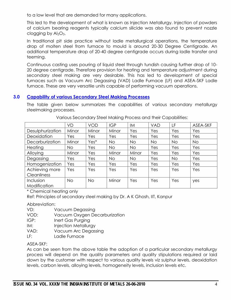
3.0 Capability of various Secondary Steel Making ProcessesThe table given below summarizes the capabilities of various secondary metallurgysteelmaking processes.
Various Secondary Steel Making Process and their Capabilities:
VD VOD IGP IM VAD LF ASEA-SKFDesulphurization Minor Minor Minor Yes Yes Yes YesDeoxidation Yes Yes Yes Yes Yes Yes YesDecarburization Minor Yes* No No No No NoHeating No Yes No No Yes Yes YesAlloying Minor Yes Minor Minor Yes Yes YesDegassing Yes Yes No No Yes No YesHomogenization Yes Yes Yes Yes Yes Yes YesAchieving moreCleanliness
Yes Yes Yes Yes Yes Yes Yes
InclusionModification
No No Minor Yes Yes Yes yes
* Chemical heating onlyRef: Principles of secondary steel making by Dr. A K Ghosh, IIT, Kanpur
Abbreviation:VD: Vacuum DegassingVOD: Vacuum Oxygen DecarburizationIGP: Inert Gas PurgingIM: Injection MetallurgyVAD: Vacuum Arc DegassingLF: Ladle Furnace
ASEA-SKF:As can be seen from the above table the adoption of a particular secondary metallurgyprocess will depend on the quality parameters and quality stipulations required or laiddown by the customer with respect to various quality levels viz sulphur levels, deoxidationlevels, carbon levels, alloying levels, homogeneity levels, inclusion levels etc.
ISSUE NO. 34 VOL. XXXIV THE INDIAN INSTITUTE OF METALS 26-06-2010 5
4.0 ConclusionsWith the increasing requirement of stringent quality stipulations and increasing demand ofspecialty steels, primary steel making in the furnace and secondary steel making in theladle have become a distinct feature of specialty steel production. Alloy and specialtysteel producers now invariably have the secondary steel making facilities for production ofquality grades meeting stringent quality demands.
CARBON FOOTPRINTK.L. Mehrotra
EX.CMDManganese Ore (India) Limited Nagpur
Vice Chairman, IIM-DC
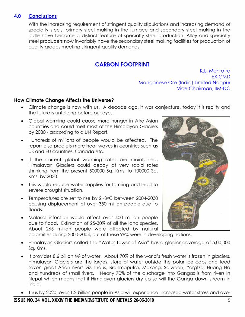
How Climate Change Affects the Universe? Climate change is now with us. A decade ago, it was conjecture, today it is reality and
the future is unfolding before our eyes.
Global warming could cause more hunger in Afro-Asiancountries and could melt most of the Himalayan Glaciersby 2030 - according to a UN Report.
Hundreds of millions of people would be affected. Thereport also predicts more heat waves in countries such asUS and EU countries, Canada etc.
If the current global warming rates are maintained,Himalayan Glaciers could decay at very rapid ratesshrinking from the present 500000 Sq. Kms. to 100000 Sq.Kms. by 2030.
This would reduce water supplies for farming and lead tosevere drought situation.
Temperatures are set to rise by 2~3oC between 2004-2030causing displacement of over 350 million people due tofloods.
Malarial infection would affect over 400 million peopledue to flood. Extinction of 25-30% of all the land species.About 265 million people were affected by naturalcalamities during 2000-2004, out of these 98% were in developing nations.
Himalayan Glaciers called the “Water Tower of Asia” has a glacier coverage of 5,00,000Sq. Kms.
It provides 8.6 billion M3 of water. About 70% of the world’s fresh water is frozen in glaciers.Himalayan Glaciers are the largest store of water outside the polar ice caps and feedseven great Asian rivers viz. Indus, Brahmaputra, Mekong, Salween, Yargtze, Huang Hoand hundreds of small rivers. Nearly 70% of the discharge into Gangas is from rivers inNepal which means that if Himalayan glaciers dry up so will the Ganga down stream inIndia.
Thus by 2020, over 1.2 billion people in Asia will experience increased water stress and over
ISSUE NO. 34 VOL. XXXIV THE INDIAN INSTITUTE OF METALS 26-06-2010 6
2.0 billion by 2030. The per capita water availability in India would drop from 1900 M3 to1000 M3 by 2025.
Cereal yield in Asia could drop by upto 30% by 2050 causing hunger.
Even modest rise in sea level will cause flooding and economic disruptions in denselypopulated areas.
Cholera/Malaria could increase, thanks to flooding and wider habitat range formosquitoes.
Some 30% Asian coral reef which sustain a large percentage of marine life are expectedto be lost in next 30 years due to climatic changes.
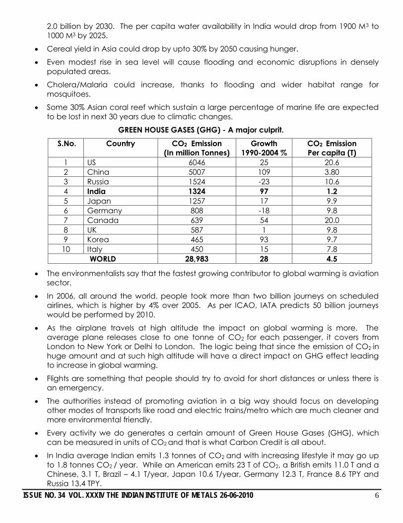
GREEN HOUSE GASES (GHG) - A major culprit.
S.No. Country CO2 Emission(In million Tonnes)
Growth1990-2004 %
CO2 EmissionPer capita (T)
1 US 6046 25 20.62 China 5007 109 3.803 Russia 1524 -23 10.64 India 1324 97 1.25 Japan 1257 17 9.96 Germany 808 -18 9.87 Canada 639 54 20.08 UK 587 1 9.89 Korea 465 93 9.710 Italy 450 15 7.8
WORLD 28,983 28 4.5
The environmentalists say that the fastest growing contributor to global warming is aviationsector.
In 2006, all around the world, people took more than two billion journeys on scheduledairlines, which is higher by 4% over 2005. As per ICAO, IATA predicts 50 billion journeyswould be performed by 2010.
As the airplane travels at high altitude the impact on global warming is more. Theaverage plane releases close to one tonne of CO2 for each passenger, it covers fromLondon to New York or Delhi to London. The logic being that since the emission of CO2 inhuge amount and at such high altitude will have a direct impact on GHG effect leadingto increase in global warming.
Flights are something that people should try to avoid for short distances or unless there isan emergency.
The authorities instead of promoting aviation in a big way should focus on developingother modes of transports like road and electric trains/metro which are much cleaner andmore environmental friendly.
Every activity we do generates a certain amount of Green House Gases (GHG), whichcan be measured in units of CO2 and that is what Carbon Credit is all about.
In India average Indian emits 1.3 tonnes of CO2 and with increasing lifestyle it may go upto 1.8 tonnes CO2 / year. While an American emits 23 T of CO2, a British emits 11.0 T and aChinese, 3.1 T, Brazil – 4.1 T/year, Japan 10.6 T/year, Germany 12.3 T, France 8.6 TPY andRussia 13.4 TPY.
ISSUE NO. 34 VOL. XXXIV THE INDIAN INSTITUTE OF METALS 26-06-2010 7
In India, the population who earns Rs. 30,000/- per month emits 5.0 TPY, between Rs.15000-30000/- - 3.1 TPY and below Rs.5000/- per month is 1.0 TPY.
If the fridge is placed away from heat / Sun, 150 Kg. of CO2 /year can be reduced more soever, energy efficient and CFL free fridge is very essential to use.
While shopping, usage of reusable bag rather than plastic / PP bags can prevent 8 Kg peryear of CO2 emission.
While brushing the teeth, if the habit of keeping the water tap open throughout, isstopped 3 Kgs. CO2 / year emission can be reduced.
55% of world carbon emission is produced by 15% of population in US, Canada, EUcountries etc.
There are three basic things which one can make a beginning.1. Reduction in usage of the planet, which we inhabit.2. Reusing of the items we use in daily life.3. Recycling of items, which may produce certain byproducts, viz paper recycling,
aluminium can recycling, pet recycling and metal scrap recycling.
If one would like to see the size of his / her Carbon Foot Print in other words, how muchtonnage of CO2 is emitted through their life style every month / year. Let’s make abeginning.
Reduce electricity consumption and switch to CFL bulbs in houses / offices in place ofincandescent bulbs / tubelights. This helps to save ½ a ton of CO2 in a year. 10,000 MWpower/per year would be saved if energy efficient CFL’s were used to light up homes inIndia.
Reduce a Petrol / Diesel by using fuel efficient car with higher mileage say 16 Kms/Ltr.,which would emit 40 T of CO2 in its lifetime say 10 years (4 T CO2 /year). We may also useBiodiesel / biofuel, admixture to reduce CO2 emissions. 660 Kg of carbon emission can bereduced if fuel is improved in car/bus engines etc.
Do not take print out, unless need arises and be conservative in use of paper. 24 grownup trees are required to be cut to produce 1 ton of paper, which has a direct impact onabsorbing CO2. One big tree absorbs 20 Kgs. of CO2 / year.
Reduce Air journey. Do it only in if it is unavoidable. Aircraft emits 12.5 kg of CO2 / perperson/100 Kms. all journey at high altitude. Thus a return journey Delhi/Mumbai or Delhi /Kolkata emits 0.33 T of CO2 per person.
As well said, for any climate change entire humanity is involved and all of us areconcerned. The GHG / CO2 emission can be attributed in two ways. Direct emission ofCO2 is due to usage of car / scooter, heavy vehicles, airplanes etc. Indirect CO2
emissions is like electricity through coal fired thermal plant, which we use, cooking gas,water supply, eating habits, shopping, etc.
CARBON TRADING: Money from CLEAN AIRWhat’s Carbon Trading?
The idea of a trade in Certified Emission Reduction of CO2 (CER) took place after signingof KYOTO PROTOCOL of UN Framework Convention of Climate Change (UNFCC).
It mandates GHG emission caps on industrialized developed nations which have ratified it
ISSUE NO. 34 VOL. XXXIV THE INDIAN INSTITUTE OF METALS 26-06-2010 8
but also allows them to buy greener nations GHG emission levels, which means a CER canbe earned by reducing emissions through eco-friendly projects. Thus a developed nationcan buy a CER from a developing country that doesn’t face a cap.
India/China are the sellers under CDM (Clean Development Mechanism) protocol. CDMallows company projects in developing countries to trade in CERs with countries that havea cap. One CER is equivalent to a reduction of one tonne of CO2.
Clean money for dirty air, that’s the promise of an emerging trade in Carbon Credit.
The value of Carbon Trading was around US 30 billion in 2006 as per the estimate ofInternational Emission Trading Association.
Till Nov. 2007, 288 CDM projects have been registered in India out of 839 CDM projectsregistered with UNFCC, giving a global share of 33%.
The CER is sold at a price negotiated between buyer and seller. Currently, Indian sellersare able to realize 12-15 Euros on an average per CER.
Hence, the CER is offered with a guarantee of delivery by the regulator. Since its launch,in April, 2005, the EU’s contract has been close to 1.3 billion tonne CO2 (CER) traded with amarket value of 24 billion euros.
Therefore carbon credits bought by a Company are a tradable permit that provides away to reduce GHG emissions by giving them a monetary value. A credit gives the ownerthe right to emit one ton of CO2.
Typically companies that invest in windmill, bio-diesel, co-generation etc., are the onesthat can generate Carbon Credits for selling to the developed nations.
Barely a day goes by without talk of climate change, the scientific report have shown, it ishappening and that human activity is responsible. If we are to move beyond talk, weneed urgent solutions. The renewable energy, carbon capture and bio-fuels are amongthe main source to mitigate climate change.
HRTEM, STEM and EELS: advance techniques for materials characterizationDr. Avanish K. Srivastava
Scientist, Electron Microscopy, Division of Materials CharacterizationCentre for Nanoscale Science, National Physical Laboratory, New Delhi
Analytical techniques capable of characterizing the nanostructure of materials are critical forcontinued growth in nano- science and devices. These techniques are highly sophisticated,sensitive and accurate for carrying out detailed investigations of the materials in terms of theircrystallographic structure, lattice imaging, phase identification, variety of defects, particle sizeand shape analysis etc. Among these, electron microscopy (SEM, TEM, HRTEM, STEM) has madesignificant advancement in the last seven decades in realizing both theory and instrumentationand has become an indispensable tool in nanomaterials characterization even at sub-nanoscale. Under a defined set of working specifications, the efficiency of the microscope isdetermined by the accelerating voltage, magnification and its resolving power. Electronmicroscopy equipped with spectroscopic measurements like energy dispersive spectroscopy(EDS) and electron energy loss spectroscopy (EELS) are beneficial in analyzing inclusions,dopants and their chemical mapping. The coupled mode of image-spectrum has been realizedas a powerful tool for determining structure – property correlation at interfaces and grain
ISSUE NO. 34 VOL. XXXIV THE INDIAN INSTITUTE OF METALS 26-06-2010 9
boundaries, local stoichiometry, impurity segregation and electronic structure pertaining toatomic states and refined electronic energy shells. Here, we demonstrate several aspects ofthese analytical techniques in dealing with various types of nanostructured materials includingsemi-conducting oxides, thin films, nanowires, different structures of nanoclusters, and cross-sectional high resolution imaging and chemistry of materials.
In a conventional transmission electron microscope (TEM), a thin specimen interacts with anelectron beam of uniform current density. The acceleration voltage of routine instrument is 100kV to 200 kV to provide better transmission and resolution and in High Voltage ElectronMicroscopy (HVEM), the acceleration voltage can be used up to 500kV-3MV. Inside the columnof the microscope, electrons are emitted in the electron gun by thermionic, schokkty or fieldemission. Field emission gun (FEG) is used when high gun brightness and coherence are needed.Electrons interact strongly with atoms by elastic and inelastic scattering. The specimen musttherefore be very thin, typically of the order of 5 to100 nm, depending on the density andelemental composition of the object and the resolution desired. The effort for the last few yearsto increase resolution have been concentrated on using a field emission gun to reduce theenergy spread ∆E from1 to 2 eV of the thermionic gun to 0.3 to 0.6 eV with FEG and thus theresolution can be improved. Specimen preparation techniques like; electropolishing and ionbeam etching in materials science and ultramicrotomy of stained and embedded tissues orcryofixation in the bio tissues, are another important aspects in the field of TEM and associatedtechniques while preparing the variety of specimens.
The significance of High Resolution Transmission Electron Microscopy (HRTEM) is that it provideshigh resolution images that contain information up to 0.1 to 0.2 nm and also operates with smallelectron probes in various microanalytical modes with a spatial resolution of 0.2 to 100 nm. Theacceleration voltage normally employed to operate HRTEM works between 200 kV to 300 kV.HRTEM is extremely useful to study and interpret the crystal structures, phase identifications,phase transformations, epitaxial growth, lattice imaging, crystallization, particle shape, particlesize, surface finish, interface structures, defects, dislocations, voids, twins, stacking faults,inclusions, precipitates and more recently several parameters pertaining to nanostructuredmaterials.
Moreover the TEM/HRTEM with Scanning Transmission Electron Microscope (STEM) mode has anadvantage that in the STEM instrument, the contrast can be enhanced by collecting severalsignals simultaneously and displaying differences and/or ratios of these by analog or digitalprocessing. In particular, single atoms on a thin substrate can be imaged with a higher contrastthan in the conventional TEM bright-or-dark field modes. An incoherent dark field mode allows ahigh resolution image of the crystal lattice to be formed, the contrast increases with increasingatomic number. The irradiation of the specimen area can be reduced to a minimum in order todecrease radiation damage. In brief, the principle of high resolution TEM (HRTEM) and scanningtransmission electron microscope (STEM) can be explained on the basis that in phase contrastimaging (HRTRM), a parallel beam irradiates the specimen, and the image is formed byinterference between many beams (i.e. direct and diffracted beams). In other case, in atomicnumber Z – contrast imaging process (STEM), a finely - focused beam with convergent angel ofnearly 10 mrad. is used for atomic resolution Z- contrast imaging. High Angle Annular Dark Field(HAADF) STEM images are formed by rastering the probe at specimen surface while the intensityof elastically scattered electrons at large angles is sequentially measured by a couple of annularscintillators. Such images are called dark field images since only scattered electrons contributeto the contrast of the image. The intensity detected is proportional to (a) number of analyzedatoms and (b) fractional power of the atomic number of given atoms.
Apart from EDS/WDS as attachment to main SEM and TEM as microanalysis tool, it is significant to
ISSUE NO. 34 VOL. XXXIV THE INDIAN INSTITUTE OF METALS 26-06-2010 10
highlight the importance of Electron Energy Loss – Spectroscopy (EELS) as an attachment withTEM and/or STEM. The basics of electron energy – loss spectroscopy (EELS) are understood as astandard method in analyzing the nano-structural observations at a very high precision. A typicalEELS spectrum consists of three main energy range, viz. (i) the smallest energy losses that aretypically of the order of 1-100 meV, arises from the excitation of phonons. As the resolution of atypical energy filter is about 1 eV, such losses may not be resolved in a microscope and aretherefore included in the zero – loss peak in which the electrons appear to be scatteredelastically, (ii) at intermediate energies (typically 1 to 50 eV) the energy losses are the primarily toa complicated mixture of single electron excitations and collective excitations (plasmons). The
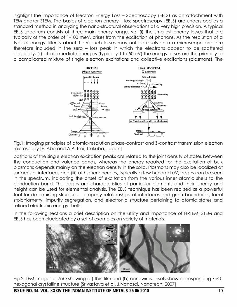
Fig.1: Imaging principles of atomic-resolution phase-contrast and Z-contrast transmission electronmicroscopy [E. Abe and A.P. Tsai, Tsukuba, Japan]
positions of the single electron excitation peaks are related to the joint density of states betweenthe conduction and valence bands, whereas the energy required for the excitation of bulkplasmons depends mainly on the electron density in the solid. Plasmons may also be localized atsurfaces or interfaces and (iii) at higher energies, typically a few hundred eV, edges can be seenin the spectrum, indicating the onset of excitation from the various inner atomic shells to theconduction band. The edges are characteristics of particular elements and their energy andheight can be used for elemental analysis. The EELS technique has been realized as a powerfultool for determining structure – property relationships at interfaces and grain boundaries, localstoichiometry, impurity segregation, and electronic structure pertaining to atomic states andrefined electronic energy shells.
In the following sections a brief description on the utility and importance of HRTEM, STEM andEELS has been elucidated by a set of examples on variety of materials.
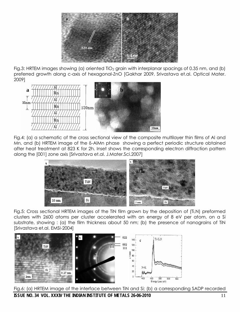
Fig.2: TEM images of ZnO showing (a) thin film and (b) nanowires. Insets show corresponding ZnO-hexagonal crystalline structure [Srivastava et.al. J.Nanosci. Nanotech. 2007]
ISSUE NO. 34 VOL. XXXIV THE INDIAN INSTITUTE OF METALS 26-06-2010 11
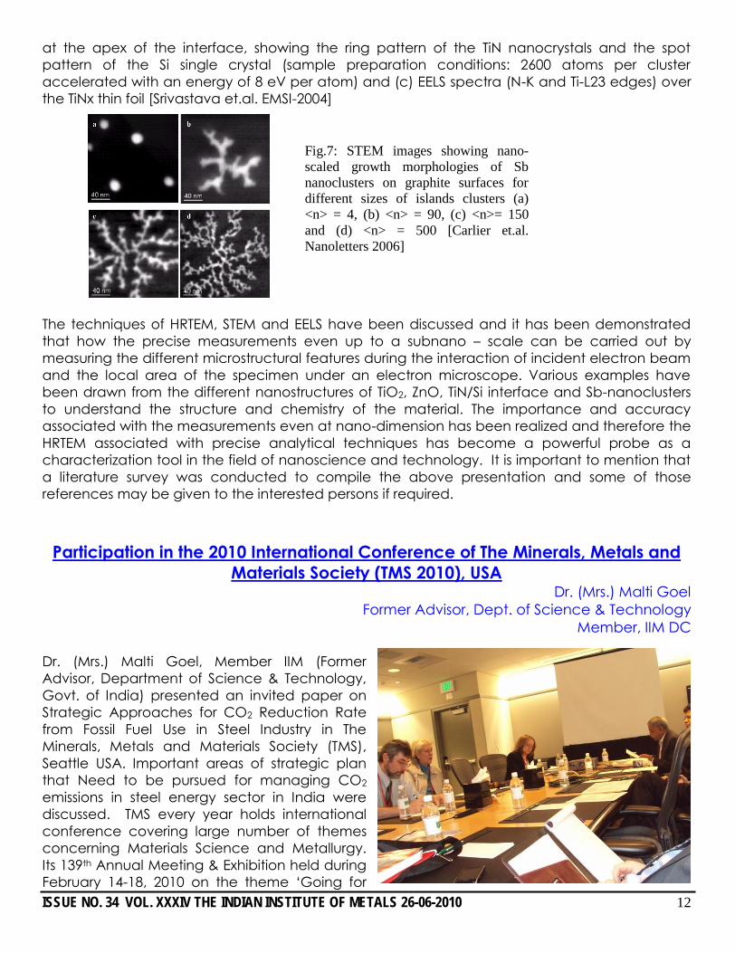
Fig.3: HRTEM images showing (a) oriented TiO2 grain with interplanar spacings of 0.35 nm, and (b)preferred growth along c-axis of hexagonal-ZnO [Gakhar 2009, Srivastava et.al. Optical Mater.2009]
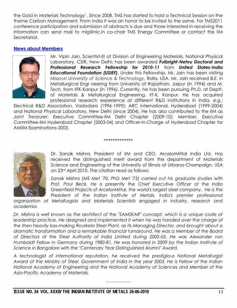
Fig.4: (a) a schematic of the cross sectional view of the composite multilayer thin films of Al andMn, and (b) HRTEM image of the δ-AlMn phase showing a perfect periodic structure obtainedafter heat treatment at 823 K for 2h. Inset shows the corresponding electron diffraction patternalong the [001] zone axis [Srivastava et.al. J.Mater.Sci.2007]
Fig.5: Cross sectional HRTEM images of the TiN film grown by the deposition of (Ti,N) preformedclusters with 2600 atoms per cluster accelerated with an energy of 8 eV per atom, on a Sisubstrate, showing : (a) the film thickness about 50 nm; (b) the presence of nanograins of TiN[Srivastava et.al. EMSI-2004]
Fig.6: (a) HRTEM image of the interface between TiN and Si; (b) a corresponding SADP recorded
a b
ISSUE NO. 34 VOL. XXXIV THE INDIAN INSTITUTE OF METALS 26-06-2010 12
at the apex of the interface, showing the ring pattern of the TiN nanocrystals and the spotpattern of the Si single crystal (sample preparation conditions: 2600 atoms per clusteraccelerated with an energy of 8 eV per atom) and (c) EELS spectra (N-K and Ti-L23 edges) overthe TiNx thin foil [Srivastava et.al. EMSI-2004]
The techniques of HRTEM, STEM and EELS have been discussed and it has been demonstratedthat how the precise measurements even up to a subnano – scale can be carried out bymeasuring the different microstructural features during the interaction of incident electron beamand the local area of the specimen under an electron microscope. Various examples havebeen drawn from the different nanostructures of TiO2, ZnO, TiN/Si interface and Sb-nanoclustersto understand the structure and chemistry of the material. The importance and accuracyassociated with the measurements even at nano-dimension has been realized and therefore theHRTEM associated with precise analytical techniques has become a powerful probe as acharacterization tool in the field of nanoscience and technology. It is important to mention thata literature survey was conducted to compile the above presentation and some of thosereferences may be given to the interested persons if required.
Participation in the 2010 International Conference of The Minerals, Metals andMaterials Society (TMS 2010), USA
Dr. (Mrs.) Malti GoelFormer Advisor, Dept. of Science & Technology
Member, IIM DC
Dr. (Mrs.) Malti Goel, Member IIM (FormerAdvisor, Department of Science & Technology,Govt. of India) presented an invited paper onStrategic Approaches for CO2 Reduction Ratefrom Fossil Fuel Use in Steel Industry in TheMinerals, Metals and Materials Society (TMS),Seattle USA. Important areas of strategic planthat Need to be pursued for managing CO2
emissions in steel energy sector in India werediscussed. TMS every year holds internationalconference covering large number of themesconcerning Materials Science and Metallurgy.Its 139th Annual Meeting & Exhibition held duringFebruary 14-18, 2010 on the theme ‘Going for
Fig.7: STEM images showing nano-scaled growth morphologies of Sbnanoclusters on graphite surfaces fordifferent sizes of islands clusters (a)<n> = 4, (b) <n> = 90, (c) <n>= 150and (d) <n> = 500 [Carlier et.al.Nanoletters 2006]
ISSUE NO. 34 VOL. XXXIV THE INDIAN INSTITUTE OF METALS 26-06-2010 13
the Gold in Materials Technology’. Since 2008, TMS has started to hold a Technical Session on thetheme Carbon Management. From India it was an honor to be invited to the same. For TMS2011conference participation and submission of abstracts is due and those interested in receiving theinformation can send mail to [email protected] co-chair TMS Energy Committee or contact the IIMSecretariat.
News about MembersMr. Vipin Jain, Scientist-EI at Division of Engineering Materials, National PhysicalLaboratory, CSIR, New Delhi; has been awarded Fulbright-Nehru Doctoral andProfessional Research Fellowship for 2010-11 from United States-IndiaEducational Foundation (USIEF). Under this Fellowship, Mr. Jain has been visitingMissouri University of Science & Technology, Rolla, USA. Mr. Jain received B.E. inMetallurgical Engi neering from University of Rajasthan, Jaipur (in 1994) and M.Tech. from IITK-Kanpur (in 1996). Currently, he has been pursuing Ph.D. at Deptt.of Materials & Metallurgical Engineering, IIT-K, Kanpur. He has acquiredprofessional research experience at different R&D institutions in India, e.g.;
Electrical R&D Association, Vadodara (1996-1999); ARC International, Hyderabad (1999-2004)and National Physical Laboratory, New Delhi (since 2004). He has also contributed to the IIM asJoint Treasurer, Executive Committee-IIM Delhi Chapter (2009-10); Member, ExecutiveCommittee-IIM Hyderabad Chapter (2003-04) and Officer-In-Charge of Hyderabad Chapter forAMIIM Examinations-2003.
*************
Dr. Sanak Mishra, President of IIM and CEO, ArcelorMittal India Ltd. Hasreceived the distinguished merit award from the department of MaterialsScience and Engineering of the University of Illinois at Urbana-Champaign, USAon 23rd April 2010. The citation read as follows:
Sanak Mishra (MS Met '70, PhD Met '73) carried out his graduate studies withProf. Paul Beck. He is presently the Chief Executive Officer of the IndiaGreenfield Projects of ArcelorMittal, the world's largest steel company. He is thePresident of the Indian Institute of Metals, India's premier professional
organization of Metallurgists and Materials Scientists engaged in industry, research andacademia.
Dr. Mishra is well known as the architect of the "SAMSKAR" concept, which is a unique code ofleadership practice. He designed and implemented it when he was handed over the charge ofthe then heavily loss-making Rourkela Steel Plant, as its Managing Director, and brought about adramatic transformation and a remarkable financial turnaround. He was a Member of the Boardof Directors of the Steel Authority of India Limited during 2002-05. He was Alexander vonHumboldt Fellow in Germany during 1980-81. He was honored in 2009 by the Indian Institute ofScience in Bangalore with the "Centenary Year Distinguished Alumni" Award.
A technologist of international reputation, he received the prestigious National MetallurgistAward of the Ministry of Steel, Government of India in the year 2003. He is Fellow of the IndianNational Academy of Engineering and the National Academy of Sciences and Member of theAsia-Pacific Academy of Materials.
……………..
ISSUE NO. 34 VOL. XXXIV THE INDIAN INSTITUTE OF METALS 26-06-2010 14
Mr. L. Pugazhenthy has been inducted as a Member, Research AdvisoryCouncil, Shri Maharshi Research Institute of Vedic Technology (SRIVT),Hyderabad. Other members of the council are (1) Dr. Baldev Raj, Director,IGCAR, (2) Dr. J S Yadav, Director, Indian Institute of Chemical Technology,(3) Prof. M Surappa, Director, IIT, Punjab, (4) Dr. Mohan Rao, Director,Centre for Cellular & Molecular Biology etc. SRIVT strives to ensure that thefruits of Vedic sciences and technologies are made available for thematerials as well spiritual prosperity of mankind. As one of the researchprojects, recently SRIVT has developed nano particles of Iron, Copper, Leadand Aluminium through the herbal route.
National NewsScientists Create Element 117London: Physicists have finally created the nuclear missing link on the list of observed elements – thesuper-heavy element 117, which is made of atoms containing 117 protons that is roughly 40 per centheavier than lead. A team from the US and Russia produced the elusive element 117 by fusingtogether atoms of calcium and another rare, heavy element known as berkelium, filling in the finalgap on the list of observed elements up to 118. Like all super-heavy atoms, elements 177 is unstable,lasting only fractions of a second before self-destructing in a cascade of lighter elements andparticles. After smashing calcium atoms into a target of berkelium in a particle accelerator at theJoint Institute for Nuclear Research in Dubna, Russia, the team deduced fleeting existence ofelement 117 by studying the daughter particles emitted as the atom decayed. Despite the atom’sshort life-time, element 117 lives longer than many lighter elements.
Courtesy: Mr. L. Pugazhenthy, ED-ILZDA & Ex. President, IIM
Check the metalHealth knows metallosis, a rare complication caused by metal implantSixty-year old Priya Gill has been complaining of knee ache sometime. Even after popping pain killersor applying analgesic gels regularly, the ache has refused to subside. Priya consults an orthopaedicwho tells her she might have metallosis. Some 10 years ago, Priya broke her knee which was fixedwith the help of a metal implant. Her doctor now suspects that the ache is due to the presence ofthe metal particles in the surrounding tissues. Or it could be that the metal particles of the implanthave loosened over time. The solution lies in Priya either getting the metal particles removed throughsurgery or get the implant replaced by a new improved version. Says Dr. Suneel Kumar, head ofdepartment, Orthopaedics, BLK Memorial Hospital, New Delhi, This is a rare complication but it doeshappen to some patients. The quality of the metal used in the implant or its specific design can leadto metallosis. Usually, a combination of metals is used in implants, the main components being highgrade stainless steel and titanium. He says whether the metal particles need to be removed isdecided after checking the patient. Each case is different. If the pain continues, we generally preferto remove it to ease the pain. Mind you, the metal particles do not cause infection. They cause onlypain.
Better ImplantsThere are no specific tests to confirm metallosis but Dr. Kumar says, “An X-ray can easily spot theproblem”. Knowledge of metallurgy, he points out, is improving every passing day which hassucceeded in making the implants for better than what they were a decade ago. Now, we get topof the design implants from abroad. Even the local implants are not bad. Apart from acute pain,which usually starts as constant dull ache, the common symptoms of metallosis are tenderness andswelling of the area.
(Contributed by Ms. Sangeetha Barooah Pisharoty, The Hindu)Courtesy: Mr. L. Pugazhenthy


![[XLS] · Web viewCHETAN JINDAL ANIL VIJAYVARGIA MOH. WAZID KHAN NARENDRA KUMAR GANPAT GANPATI CONNECT VIKRAM GIL GHANSHYAM RANKAWAT FALGUN MITTAL GOPAL LAL CHOUDHARY RAMESH](https://img.pdfslide.us/doc/110x75/5aaea7dd7f8b9a59478c5817/xls-viewchetan-jindal-anil-vijayvargia-moh-wazid-khan-narendra-kumar-ganpat-ganpati.jpg)