Embed Size (px)
Citation preview

VLSI Physical Design: From Graph Partitioning to Timing Closure Chapter 8: Timing Closure 1
©K
LM
H
Lie
nig
Chapter 8 – Timing Closure
8.1 Introduction
8.2 Timing Analysis and Performance Constraints
8.2.1 Static Timing Analysis
8.2.2 Delay Budgeting with the Zero-Slack Algorithm
8.3 Timing-Driven Placement
8.3.1 Net-Based Techniques
8.3.2 Embedding STA into Linear Programs for Placement
8.4 Timing-Driven Routing
8.4.1 The Bounded-Radius, Bounded-Cost Algorithm
8.4.2 Prim-Dijkstra Tradeoff
8.4.3 Minimization of Source-to-Sink Delay
8.5 Physical Synthesis
8.5.1 Gate Sizing
8.5.2 Buffering
8.5.3 Netlist Restructuring
8.6 Performance-Driven Design Flow
8.7 Conclusions

VLSI Physical Design: From Graph Partitioning to Timing Closure Chapter 8: Timing Closure 2
©K
LM
H
Lie
nig
ENTITY test is
port a: in bit;
end ENTITY test;
DRC
LVS
ERC
Circuit Design
Functional Design
and Logic Design
Physical Design
Physical Verification
and Signoff
Fabrication
System Specification
Architectural Design
Chip
Packaging and Testing
Chip Planning
Placement
Signal Routing
Partitioning
Timing Closure
Clock Tree Synthesis
8.1 Introduction

VLSI Physical Design: From Graph Partitioning to Timing Closure Chapter 8: Timing Closure 3
©K
LM
H
Lie
nig
• IC layout must satisfy geometric constraints and timing constraints
− Setup (long-path) constraints
− Hold (short-path) constraints
• Chip designers must complete timing closure
− Optimization process that meets timing constraints
− Integrates point optimizations discussed in previous chapters, e.g.,
placement and routing, with specialized methods to improve circuit performance
8.1 Introduction

VLSI Physical Design: From Graph Partitioning to Timing Closure Chapter 8: Timing Closure 4
©K
LM
H
Lie
nig
Components of timing closure covered in this lecture:
• Timing-driven placement (Sec. 8.3) minimizes signal delays
when assigning locations to circuit elements
• Timing-driven routing (Sec. 8.4) minimizes signal delays
when selecting routing topologies and specific routes
• Physical synthesis (Sec. 8.5) improves timing by changing the netlist.
− Sizing transistors or gates: increasing the width:length ratio of transistors
to decrease the delay or increase the drive strength of a gate
− Inserting buffers into nets to decrease propagation delays
− Restructuring the circuit along its critical paths
• Performance-driven physical design flow (Sec. 8.6)
8.1 Introduction

VLSI Physical Design: From Graph Partitioning to Timing Closure Chapter 8: Timing Closure 5
©K
LM
H
Lie
nig
• Timing optimization engines must estimate circuit delays quickly and accurately
to improve circuit timing
• Timing optimizers adjust propagation delays through circuit components,
with the primary goal of satisfying timing constraints, including
− Setup (long-path) constraints, which specify the amount of time a data input signal
should be stable (steady) before the clock edge for each storage element
(e.g., flip-flop or latch)
− Hold-time (short-path) constraints, which specify the amount of time a data input
signal should be stable after the clock edge at each storage element
8.1 Introduction
skewsetupcombDelaycycle tttt ++≥ skewholdcombDelay ttt +≥

VLSI Physical Design: From Graph Partitioning to Timing Closure Chapter 8: Timing Closure 6
©K
LM
H
Lie
nig
• Timing closure is the process of satisfying timing constraints
through layout optimizations and netlist modifications
• Industry jargon: “the design has closed timing”
8.1 Introduction

VLSI Physical Design: From Graph Partitioning to Timing Closure Chapter 8: Timing Closure 7
©K
LM
H
Lie
nig
8.1 Introduction
8.2 Timing Analysis and Performance Constraints
8.2.1 Static Timing Analysis
8.2.2 Delay Budgeting with the Zero-Slack Algorithm
8.3 Timing-Driven Placement
8.3.1 Net-Based Techniques
8.3.2 Embedding STA into Linear Programs for Placement
8.4 Timing-Driven Routing
8.4.1 The Bounded-Radius, Bounded-Cost Algorithm
8.4.2 Prim-Dijkstra Tradeoff
8.4.3 Minimization of Source-to-Sink Delay
8.5 Physical Synthesis
8.5.1 Gate Sizing
8.5.2 Buffering
8.5.3 Netlist Restructuring
8.6 Performance-Driven Design Flow
8.7 Conclusions
8.2 Timing Analysis and Performance Constraints
VLSI Physical Design: From Graph Partitioning to Timing Closure Chapter 8: Timing Closure 8
©K
LM
H
Lie
nig
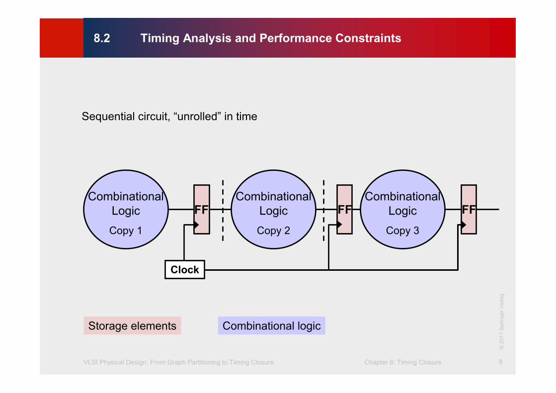
Sequential circuit, “unrolled” in time
Clock
FFCombinational
Logic
Copy 1
FFCombinational
Logic
Copy 3
FFCombinational
Logic
Copy 2
Storage elements Combinational logic
8.2 Timing Analysis and Performance Constraints
©201
1 S
pring
er
Verlag

VLSI Physical Design: From Graph Partitioning to Timing Closure Chapter 8: Timing Closure 9
©K
LM
H
Lie
nig
• Main delay concerns in sequential circuits
− Gate delays are due to gate transitions
− Wire delays are due to signal propagation along wires
− Clock skew is due to the difference in time the sequential elements activate
• Need to quickly estimate sequential circuit timing
− Perform static timing analysis (STA)
− Assume clock skew is negligible, postpone until after clock network synthesis
8.2 Timing Analysis and Performance Constraints
VLSI Physical Design: From Graph Partitioning to Timing Closure Chapter 8: Timing Closure 10
©K
LM
H
Lie
nig
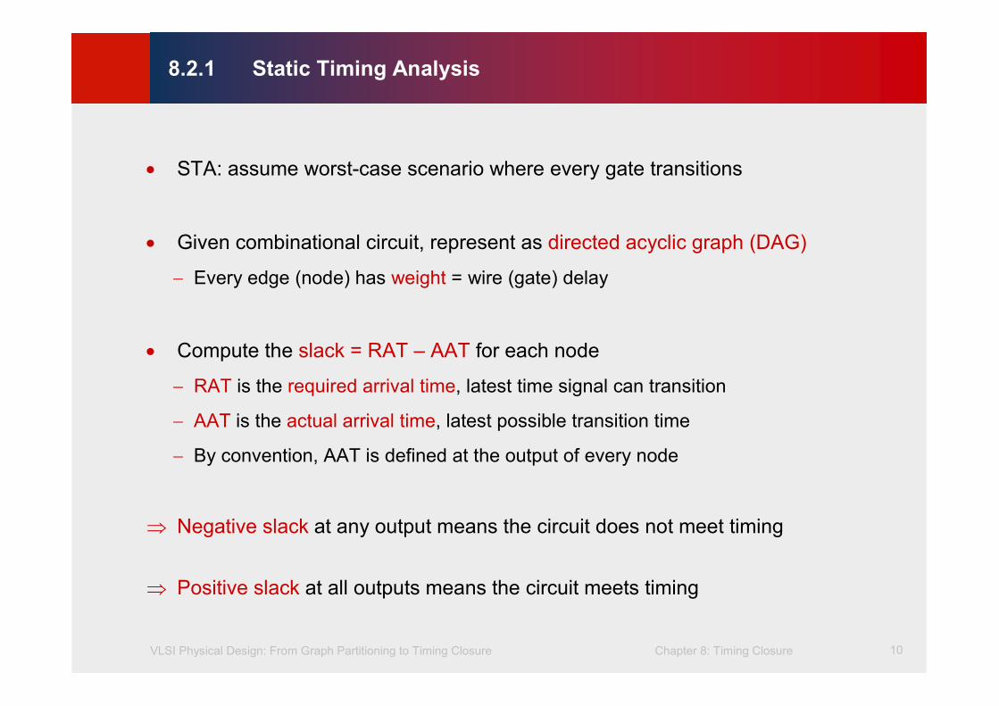
• STA: assume worst-case scenario where every gate transitions
• Given combinational circuit, represent as directed acyclic graph (DAG)
− Every edge (node) has weight = wire (gate) delay
• Compute the slack = RAT – AAT for each node
− RAT is the required arrival time, latest time signal can transition
− AAT is the actual arrival time, latest possible transition time
− By convention, AAT is defined at the output of every node
⇒ Negative slack at any output means the circuit does not meet timing
⇒ Positive slack at all outputs means the circuit meets timing
8.2.1 Static Timing Analysis

VLSI Physical Design: From Graph Partitioning to Timing Closure Chapter 8: Timing Closure 11
©K
LM
H
Lie
nig
Combinational circuit as DAG
(0.15)
(0.1) (0.3)
(0.2)
b
a
c
fy (2)
w (2)
(0.1)
(0.2)
(0.1)
(0.25)x (1)z (2)
(0.15)
(0.1)
(0.1)
(0.1) (0.2)
(0.25)
(0.2)(0)
(0)
(0.6) (0.3)
x (1)
y (2)
z (2)
w (2) f (0)
a (0)
b (0)
c (0)
s
8.2.1 Static Timing Analysis
©201
1 S
pring
er
Verlag

VLSI Physical Design: From Graph Partitioning to Timing Closure Chapter 8: Timing Closure 12
©K
LM
H
Lie
nig
Compute AATs at each node:
where FI(v) is the fanin nodes, and t(u,v) is the delay between u and v
A 0.6
A 5.85A 5.65A 0 A 1.1A 0
A 0
A 3.4
A 3.2
( )),()(max)()(
vutuAATvAATvFIu
+=∈
8.2.1 Static Timing Analysis
©201
1 S
pring
er
Verlag
(AATs of inputs are given)
(0.15)
(0.1)
(0.1)
(0.1) (0.2)
(0.25)
(0.2)(0)
(0)
(0.6) (0.3)
x (1)
y (2)
z (2)
w (2) f (0)
a (0)
b (0)
c (0)
s

VLSI Physical Design: From Graph Partitioning to Timing Closure Chapter 8: Timing Closure 13
©K
LM
H
Lie
nig
Compute RATs at each node:
where FO(v) are the fanout nodes, and t(u,v) is the delay between u and v
( )),()(max)()(
vutuRATvRATvFOu
−=∈
(0.15)
(0.1)
(0.1)
(0.1) (0.2)
(0.25)
(0.2)(0)
(0)
(0.6) (0.3)
x (1)
y (2)
z (2)
w (2) f (0)
a (0)
b (0)
c (0)
s
R 0.95
R 0.95
R 5.5
R 3.1
R 5.3R -0.35 R 0.75
R 3.05
R -0.35
8.2.1 Static Timing Analysis
©201
1 S
pring
er
Verlag
(RATs of outputs are given)

VLSI Physical Design: From Graph Partitioning to Timing Closure Chapter 8: Timing Closure 14
©K
LM
H
Lie
nig
Compute slacks at each node:
)()()( vAATvRATvslack −=
(0.15)
(0.1)
(0.1)
(0.1) (0.2)
(0.25)
(0.2)(0)
(0)
(0.6) (0.3)
x (1)
y (2)
z (2)
w (2) f (0)
a (0)
b (0)
c (0)
s
A 0R 0.95S 0.95
A 0R -0.35S -0.35
A 0R -0.35S -0.35
A 0.6R 0.95S 0.35
A 1.1R 0.75S -0.35
A 3.4R 3.05S -0.35
A 3.2R 3.1S -0.1
A 5.65R 5.3S -0.35
A 5.85R 5.5S -0.35
8.2.1 Static Timing Analysis
©201
1 S
pring
er
Verlag

VLSI Physical Design: From Graph Partitioning to Timing Closure Chapter 8: Timing Closure 15
©K
LM
H
Lie
nig
• Establish timing budgets for nets
− Gate and wire delays must be optimized during timing driven layout design
− Wire delays depend on wire lengths
− Wire lengths are not known until after placement and routing
• Delay budgeting with the zero-slack algorithm
− Let vi be the logic gates
− Let ei be the nets
− Let DELAY(v) and DELAY(e) be the delay of the gate and net, respectively
− Define the timing budget of a gate TB(v) = DELAY(v) + DELAY(e)
8.2.2 Delay Budgeting with the Zero-Slack Algorithm

VLSI Physical Design: From Graph Partitioning to Timing Closure Chapter 8: Timing Closure 16
©K
LM
H
Lie
nig
Input: timing graph G(V,E)
Output: timing budgets TB for each v ∈ V
1. do
2. (AAT,RAT,slack) = STA(G)
3. foreach (vi ∈ V)
4. TB[vi] = DELAY(vi) + DELAY(ei)
5. slackmin = ∞
6. foreach (v ∈ V)
7. if ((slack[v] < slackmin) and (slack[v] > 0))
8. slackmin = slack[v]
9. vmin = v
10. if (slackmin≠∞)
11. path = vmin
12. ADD_TO_FRONT(path,BACKWARD_PATH(vmin,G))
13. ADD_TO_BACK(path,FORWARD_PATH(vmin,G))
14. s = slackmin / |path|
15. for (i = 1 to |path|)
16. node = path[i] // evenly distribute
17. TB[node] = TB[node] + s // slack along path
18. while (slackmin≠∞)
8.2.2 Delay Budgeting with the Zero-Slack Algorithm

VLSI Physical Design: From Graph Partitioning to Timing Closure Chapter 8: Timing Closure 17
©K
LM
H
Lie
nig
Forward Path Search (FORWARD_PATH(vmin
,G))
Input: node vmin with minimum slack slackmin, timing graph G
Output: maximal downstream path path from vmin such that no node v ∈ V affects
the slack of path
1. path = vmin
2. do
3. flag = false
4. node = LAST_ELEMENT(path)
5. foreach (fanout node fo of node)
6. if ((RAT[fo] == RAT[node] + TB[fo]) and (AAT[fo] == AAT[node] + TB[fo]))
7. ADD_TO_BACK(path,fo)
8. flag = true
9. break
10. while (flag == true)
11. REMOVE_FIRST_ELEMENT(path) // remove vmin
8.2.2 Delay Budgeting with the Zero-Slack Algorithm

VLSI Physical Design: From Graph Partitioning to Timing Closure Chapter 8: Timing Closure 18
©K
LM
H
Lie
nig
Backward Path Search (BACKWARD_PATH(vmin
,G))
Input: node vmin with minimum slack slackmin, timing graph G
Output: maximal upstream path path from vmin such that no node v ∈ V affects the
slack of path
1. path = vmin
2. do
3. flag = false
4. node = FIRST_ELEMENT(path)
5. foreach (fanin node fi of node)
6. if ((RAT[fi] == RAT[node] – TB[fi]) and (AAT[fi] == AAT[node] – TB[fi]))
7. ADD_TO_FRONT(path,fi)
8. flag = true
9. break
10. while (flag == true)
11. REMOVE_LAST_ELEMENT(path) // remove vmin
8.2.2 Delay Budgeting with the Zero-Slack Algorithm

VLSI Physical Design: From Graph Partitioning to Timing Closure Chapter 8: Timing Closure 19
©K
LM
H
Lie
nig
8.1 Introduction
8.2 Timing Analysis and Performance Constraints
8.2.1 Static Timing Analysis
8.2.2 Delay Budgeting with the Zero-Slack Algorithm
8.3 Timing-Driven Placement
8.3.1 Net-Based Techniques
8.3.2 Embedding STA into Linear Programs for Placement
8.4 Timing-Driven Routing
8.4.1 The Bounded-Radius, Bounded-Cost Algorithm
8.4.2 Prim-Dijkstra Tradeoff
8.4.3 Minimization of Source-to-Sink Delay
8.5 Physical Synthesis
8.5.1 Gate Sizing
8.5.2 Buffering
8.5.3 Netlist Restructuring
8.6 Performance-Driven Design Flow
8.7 Conclusions
8.3 Timing-Driven Placement

VLSI Physical Design: From Graph Partitioning to Timing Closure Chapter 8: Timing Closure 20
©K
LM
H
Lie
nig
• Timing-driven placement optimizes circuit delay
• Let T be the set of all timing endpoints
• Circuit delay is measured by worst negative slack (WNS)
• Or total negative slack (TNS)
• Classifications: net-based, path-based, integrated
( ))τ(minτ
slackWNSΤ∈
=
∑<Τ∈
=0)τ(,τ
)τ(
slack
slackTNS
8.3 Timing-Driven Placement

VLSI Physical Design: From Graph Partitioning to Timing Closure Chapter 8: Timing Closure 21
©K
LM
H
Lie
nig
• Net weights are added to each net – placer optimizes weighted wirelength
• Static net weights: computed before placement (never changes)
− Discrete net weights: where ω1 > 0, ω2 > 0, and ω2 > ω1
− Continuous net weights: where t is the longest path delay
and α is a criticality exponent
− Based on net sensitivity to TNS and slack
≤
>=
0 if ω
0 if ω
2
1
slack
slackw
α
1
−=t
slackw
TNSw
SLACKwtargeto sβsslackslackww ⋅+⋅−+= )(α
8.3.1 Net-Based Techniques

VLSI Physical Design: From Graph Partitioning to Timing Closure Chapter 8: Timing Closure 22
©K
LM
H
Lie
nig
• Dynamic net weights: (re)computed during placement
− Estimate slack at every iteration:
where ∆L is the change in wirelength
− Update net criticality:
− Update net weight:
• Variations include updating every j iterations, different relations
between criticality and net weight
Lsslackslack DELAYLkk ∆⋅−= −1
( )
+
=
−
−
1
1
υ2
1
1υ2
1
υ
k
k
k
if among the top 3% of critical nets
otherwise
( )kkk ww υ11 +⋅= −
8.3.1 Net-Based Techniques
VLSI Physical Design: From Graph Partitioning to Timing Closure Chapter 8: Timing Closure 23
©K
LM
H
Lie
nig
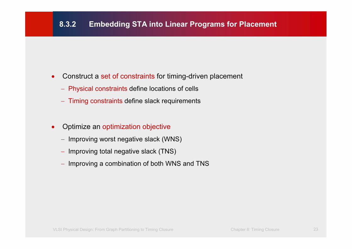
• Construct a set of constraints for timing-driven placement
− Physical constraints define locations of cells
− Timing constraints define slack requirements
• Optimize an optimization objective
− Improving worst negative slack (WNS)
− Improving total negative slack (TNS)
− Improving a combination of both WNS and TNS
8.3.2 Embedding STA into Linear Programs for Placement
VLSI Physical Design: From Graph Partitioning to Timing Closure Chapter 8: Timing Closure 24
©K
LM
H
Lie
nig
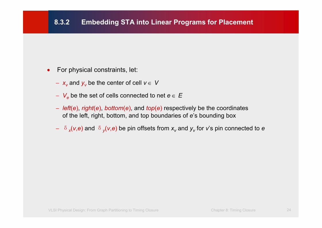
• For physical constraints, let:
− xv and yv be the center of cell v ∈ V
− Ve be the set of cells connected to net e ∈ E
− left(e), right(e), bottom(e), and top(e) respectively be the coordinates
of the left, right, bottom, and top boundaries of e’s bounding box
− δx(v,e) and δy(v,e) be pin offsets from xv and yv for v’s pin connected to e
8.3.2 Embedding STA into Linear Programs for Placement

VLSI Physical Design: From Graph Partitioning to Timing Closure Chapter 8: Timing Closure 25
©K
LM
H
Lie
nig
• Then, for all v ∈ Ve:
• Define e’s half-perimeter wirelength (HPWL):
),(δ)(
),(δ)(
),(δ)(
),(δ)(
evyetop
evyebottom
evxeright
evxeleft
yv
yv
xv
xv
+≥
+≤
+≥
+≤
)()()()()( ebottometopelefterighteL −+−=
8.3.2 Embedding STA into Linear Programs for Placement

VLSI Physical Design: From Graph Partitioning to Timing Closure Chapter 8: Timing Closure 26
©K
LM
H
Lie
nig
• For timing constraints, let
− tGATE(vi,vo) be the gate delay from an input pin vi to the output pin vo for cell v
− tNET(e,uo,vi) be net e’s delay from cell u’s output pin uo to cell v’s input pin vi
− AAT(vj) be the arrival time on pin j of cell v
8.3.2 Embedding STA into Linear Programs for Placement

VLSI Physical Design: From Graph Partitioning to Timing Closure Chapter 8: Timing Closure 27
©K
LM
H
Lie
nig
• For every input pin vi of cell v :
• For every output pin vo of cell v :
• For every pin τp in a sequential cellτ:
• Ensure that every slack(τp) ≤ 0
),()()( ioNEToi vutuAATvAAT +=
),()()( oiGATEio vvtvAATvAAT +≥
)τ()τ()τ( ppp AATRATslack −≤
8.3.2 Embedding STA into Linear Programs for Placement

VLSI Physical Design: From Graph Partitioning to Timing Closure Chapter 8: Timing Closure 28
©K
LM
H
Lie
nig
• Optimize for total negative slack:
• Optimize for worst negative slack:
• Optimize for both TNS and WNS:
∑Τ∈∈ τ),τ(τ
)τ(:max
Pins
p
p
slack
WNS:max
∑∈
⋅−Ee
WNSeL α)(:min
8.3.2 Embedding STA into Linear Programs for Placement

VLSI Physical Design: From Graph Partitioning to Timing Closure Chapter 8: Timing Closure 29
©K
LM
H
Lie
nig
8.1 Introduction
8.2 Timing Analysis and Performance Constraints
8.2.1 Static Timing Analysis
8.2.2 Delay Budgeting with the Zero-Slack Algorithm
8.3 Timing-Driven Placement
8.3.1 Net-Based Techniques
8.3.2 Embedding STA into Linear Programs for Placement
8.4 Timing-Driven Routing
8.4.1 The Bounded-Radius, Bounded-Cost Algorithm
8.4.2 Prim-Dijkstra Tradeoff
8.4.3 Minimization of Source-to-Sink Delay
8.5 Physical Synthesis
8.5.1 Gate Sizing
8.5.2 Buffering
8.5.3 Netlist Restructuring
8.6 Performance-Driven Design Flow
8.7 Conclusions
8.4 Timing-Driven Routing

VLSI Physical Design: From Graph Partitioning to Timing Closure Chapter 8: Timing Closure 30
©K
LM
H
Lie
nig
• Timing-driven routing seeks to minimize:
− Maximum sink delay: delay from the source to any sink in a net
− Total wirelength: routed length of the net
• For a signal net net, let
− s0 be the source node
− sinks = {s1, … ,sn} be the sinks
− G = (V,E) be a corresponding weighted graph where:
− V = {v0,v1, … ,vn} represents the source and sink nodes of net, and
− the weight of an edge e(vi,vj) ∈ E represents the routing cost between vi and vj
8.4 Timing-Driven Routing

VLSI Physical Design: From Graph Partitioning to Timing Closure Chapter 8: Timing Closure 31
©K
LM
H
Lie
nig
• For any spanning tree T over G, let:
− radius(T) be the length of the longest source-sink path in T
− cost(T) be the total edge weight of T
• Trade off between “shallow” and “light” trees
• “Shallow” trees have minimum radius
− Shortest-paths tree
− Constructed by Dijkstra’s Algorithm
• “Light” trees have minimum cost
− Minimum spanning tree (MST)
− Constructed by Prim’s Algorithm
8.4 Timing-Driven Routing

VLSI Physical Design: From Graph Partitioning to Timing Closure Chapter 8: Timing Closure 32
©K
LM
H
Lie
nig
radius(T) = 8
cost(T) = 20
“Shallow”
s0
6
5
7
2
s0
3
5
2
3
radius(T) = 13
cost(T) = 13
“Light”
s0
6
5
2
3
radius(T) = 11
cost(T) = 16
Tradeoff between
shallow and light
8.4 Timing-Driven Routing
©201
1 S
pring
er
Verlag

VLSI Physical Design: From Graph Partitioning to Timing Closure Chapter 8: Timing Closure 33
©K
LM
H
Lie
nig
• Trades off radius for cost by setting upper bounds on both
• In the bounded-radius, bounded-cost (BRBC) algorithm, let:
− TS be the shortest-paths tree
− TM be the minimum spanning tree
• TBRBC is the tree constructed with parameter ε that satisfies:
• When ε = 0, TBRBC has minimum radius
• When ε = ∞, TBRBC has minimum cost
)()ε1()( SBRBC TradiusTradius ⋅+≤and
)(ε
21)( MBRBC TcostTcost ⋅
+≤
8.4.1 The Bounded-Radius, Bounded-Cost Algorithm

VLSI Physical Design: From Graph Partitioning to Timing Closure Chapter 8: Timing Closure 34
©K
LM
H
Lie
nig
• Prim-Dijkstra Tradeoff based on Prim’s algorithm and Dijkstra’s algorithm
• From the set of sinks S, iteratively add sink s based on different cost function
− Prim’s algorithm cost function:
− Dijkstra’s algorithm cost function:
− Prim-Dijkstra Tradeoff cost function:
• γ is a constant between 0 and 1
),( ji sscost
),(),( 0 jii sscostsscost +
),(),(γ 0 jii sscostsscost +⋅
8.4.2 Prim-Dijkstra Tradeoff

VLSI Physical Design: From Graph Partitioning to Timing Closure Chapter 8: Timing Closure 35
©K
LM
H
Lie
nig
s0
78
9
7
4
s0
78
9
11
4
radius(T) = 19
cost(T) = 35
γ = 0.25
radius(T) = 15
cost(T) = 39
γ = 0.75
8.4.2 Prim-Dijkstra Tradeoff
©201
1 S
pring
er
Verlag

VLSI Physical Design: From Graph Partitioning to Timing Closure Chapter 8: Timing Closure 36
©K
LM
H
Lie
nig
• Iteratively forms a tree by adding sinks, and optimizes for critical sink(s)
• In the critical-sink routing tree (CSRT) problem, minimize:
where α(i) are sink criticalities for sinks si, and t(s0,si) is the delay from s0 to si
∑=
⋅n
i
issti
1
0 ),()(α
8.4.3 Minimization of Source-to-Sink Delay

VLSI Physical Design: From Graph Partitioning to Timing Closure Chapter 8: Timing Closure 37
©K
LM
H
Lie
nig
• In the critical-sink Steiner tree problem, construct a
minimum-cost Steiner tree T for all sinks except for the most critical sink sc
• Add in the critical sink by:
− H0: a single wire from sc to s0
− H1: the shortest possible wire that can join sc to T, so long as the path
from s0 to sc is the shortest possible total length
− HBest: try all shortest connections from sc to edges in T and from sc to s0.
Perform timing analysis on each of these trees and pick the one
with the lowest delay at sc
8.4.3 Minimization of Source-to-Sink Delay

VLSI Physical Design: From Graph Partitioning to Timing Closure Chapter 8: Timing Closure 38
©K
LM
H
Lie
nig
8.1 Introduction
8.2 Timing Analysis and Performance Constraints
8.2.1 Static Timing Analysis
8.2.2 Delay Budgeting with the Zero-Slack Algorithm
8.3 Timing-Driven Placement
8.3.1 Net-Based Techniques
8.3.2 Embedding STA into Linear Programs for Placement
8.4 Timing-Driven Routing
8.4.1 The Bounded-Radius, Bounded-Cost Algorithm
8.4.2 Prim-Dijkstra Tradeoff
8.4.3 Minimization of Source-to-Sink Delay
8.5 Physical Synthesis
8.5.1 Gate Sizing
8.5.2 Buffering
8.5.3 Netlist Restructuring
8.6 Performance-Driven Design Flow
8.7 Conclusions
8.5 Physical Synthesis

VLSI Physical Design: From Graph Partitioning to Timing Closure Chapter 8: Timing Closure 39
©K
LM
H
Lie
nig
• Physical synthesis is a collection of timing optimizations to fix negative slack
• Consists of creating timing budgets and performing timing corrections
• Timing budgets include:
− allocating target delays along paths or nets
− often during placement and routing stages
− can also be during timing correction operations
• Timing corrections include:
− gate sizing
− buffer insertion
− netlist restructuring
8.5 Physical Synthesis

VLSI Physical Design: From Graph Partitioning to Timing Closure Chapter 8: Timing Closure 40
©K
LM
H
Lie
nig
• Let a gate v have 3 sizes A, B, C, where:
• Gate with a larger size has lower output resistance
• When load capacitances are large:
• Gate with a smaller size has higher output resistance
• When load capacitances are small:
)()()( ABC vtvtvt <<
)()()( ABC vsizevsizevsize >>
)()()( ABC vtvtvt >>
8.5.1 Gate Sizing

VLSI Physical Design: From Graph Partitioning to Timing Closure Chapter 8: Timing Closure 41
©K
LM
H
Lie
nig
24
5
10
15
20
25
0.5
30
35
40
Dela
y (
ps)
Load Capacitance (fF)
1.0 1.5 2.0 2.5 3.0
40
35
30
25
20
15
1821 24
27
30
33
23 26 2728
C
B
A
8.5.1 Gate Sizing
• Let a gate v have 3 sizes A, B, C, where: )()()( ABC vsizevsizevsize >>
©201
1 S
pring
er
Verlag

VLSI Physical Design: From Graph Partitioning to Timing Closure Chapter 8: Timing Closure 42
©K
LM
H
Lie
nig
b
ad
e
f
C(d) = 1.5
C(e) = 1.0
C(f) = 0.5
v
b
ad
e
f
C(d) = 1.5
C(e) = 1.0
C(f) = 0.5
t(vA) = 40
vA b
ad
e
f
C(d) = 1.5
C(e) = 1.0
C(f) = 0.5
t(vC) = 28
vC
8.5.1 Gate Sizing
VLSI Physical Design: From Graph Partitioning to Timing Closure Chapter 8: Timing Closure 43
©K
LM
H
Lie
nig
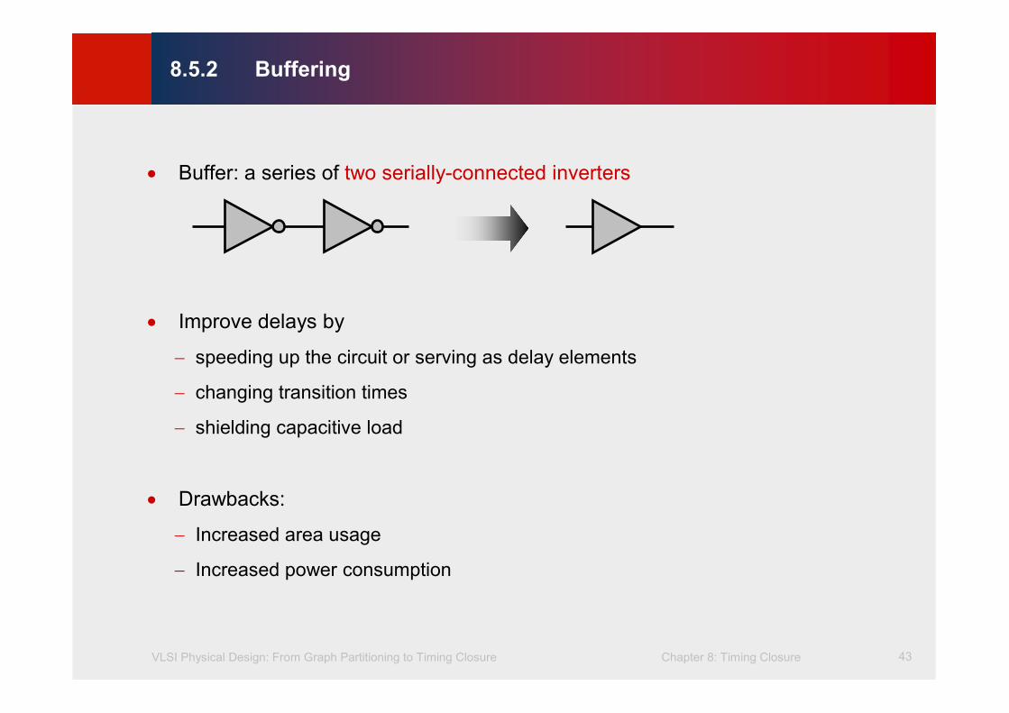
• Buffer: a series of two serially-connected inverters
• Improve delays by
− speeding up the circuit or serving as delay elements
− changing transition times
− shielding capacitive load
• Drawbacks:
− Increased area usage
− Increased power consumption
8.5.2 Buffering

VLSI Physical Design: From Graph Partitioning to Timing Closure Chapter 8: Timing Closure 44
©K
LM
H
Lie
nig
d
e
f
g
h
C(e) = 1
C(d) = 1
C(f) = 1
C(g) = 1
C(h) = 1
b
avB b
a
d
e
f
g
h
C(e) = 1
C(d) = 1
C(f) = 1
C(g) = 1
C(h) = 1
vBy
C(vB) = 5 fF
t(vB) = 45 ps
C(vB) = 3 fF
t(vB) = 33 ps
C(y) = 3 fF
t(y) = t(vB) + t(y) = 66 ps
8.5.2 Buffering

VLSI Physical Design: From Graph Partitioning to Timing Closure Chapter 8: Timing Closure 45
©K
LM
H
Lie
nig
• Netlist restructuring only changes existing gates, does not change functionality
• Changes include
− Cloning: duplicating gates
− Redesign of fanin or fanout tree: changing the topology of gates
− Swapping communicative pins: changing the connections
− Gate decomposition: e.g., changing AND-OR to NAND-NAND
− Boolean restructuring: e.g., applying Boolean laws to change circuit gates
• Can also do reverse transformations of above, e.g., downsizing, merging
8.5.3 Netlist Restructuring

VLSI Physical Design: From Graph Partitioning to Timing Closure Chapter 8: Timing Closure 46
©K
LM
H
Lie
nig
• Cloning can reduce fanout capacitance
• and reduce downstream capacitance
d
e
f
g
h
C(e) = 1
C(d) = 1
C(f) = 1
C(g) = 1
C(h) = 1
b
a b
a d
e
f
g
h
vB
vA
vB
C(e) = 1
C(d) = 1
C(f) = 1
C(g) = 1
C(h) = 1
d
e
f
g
h
b
ab
ad
e
f
…
v
v
…g
h
v’ …
8.5.3 Netlist Restructuring
©201
1 S
pring
er
Verlag

VLSI Physical Design: From Graph Partitioning to Timing Closure Chapter 8: Timing Closure 47
©K
LM
H
Lie
nig
Redesigning the fanin tree can change AATs
(1)
(1)
(1)
a <4>
b <3>
c <1>
d <0>
f <6>
(1)
(1)
(1)a <4>
b <3>
c <1>
d <0>
f <5>
8.5.3 Netlist Restructuring
©201
1 S
pring
er
Verlag

VLSI Physical Design: From Graph Partitioning to Timing Closure Chapter 8: Timing Closure 48
©K
LM
H
Lie
nig
Redesigning fanout trees can change delays on specific paths
path1
path2
(1)
y1 (1)
y2 (1)
(1)
path1
path2
y2 (1)
(1)(1)
8.5.3 Netlist Restructuring
©201
1 S
pring
er
Verlag

VLSI Physical Design: From Graph Partitioning to Timing Closure Chapter 8: Timing Closure 49
©K
LM
H
Lie
nig
Swapping communicative pins can change the final delay
(1)(1)
(2)
(1)
a <0>
b <1>
c <2>
f <5>(1)(1)
(2)
(1)
a <0>
b <1>
c <2>f <3>
8.5.3 Netlist Restructuring
©201
1 S
pring
er
Verlag

VLSI Physical Design: From Graph Partitioning to Timing Closure Chapter 8: Timing Closure 50
©K
LM
H
Lie
nig
Gate decomposition can change the general structure of the circuit
8.5.3 Netlist Restructuring
©201
1 S
pring
er
Verlag

VLSI Physical Design: From Graph Partitioning to Timing Closure Chapter 8: Timing Closure 51
©K
LM
H
Lie
nig
8.5.3 Netlist Restructuring
Boolean restructuring uses laws or properties,
e.g., distributive law, to change circuit topology
(a + b)(a + c) = a + bc
(1)a <4>
b <1>
c <2>(1)
(1)
(1)
(1)
x <6>
y <6>
x(a,b,c) = (a + b)(a + c)
y(a,b,c) = (a + c)(b + c)
(1)
(1)
(1)
(1)
x <5>
y <6>
a <4>
b <1>
c <2>
x(a,b,c) = a + bc
y(a,b,c) = ab + c
©201
1 S
pring
er
Verlag

VLSI Physical Design: From Graph Partitioning to Timing Closure Chapter 8: Timing Closure 52
©K
LM
H
Lie
nig
8.1 Introduction
8.2 Timing Analysis and Performance Constraints
8.2.1 Static Timing Analysis
8.2.2 Delay Budgeting with the Zero-Slack Algorithm
8.3 Timing-Driven Placement
8.3.1 Net-Based Techniques
8.3.2 Embedding STA into Linear Programs for Placement
8.4 Timing-Driven Routing
8.4.1 The Bounded-Radius, Bounded-Cost Algorithm
8.4.2 Prim-Dijkstra Tradeoff
8.4.3 Minimization of Source-to-Sink Delay
8.5 Physical Synthesis
8.5.1 Gate Sizing
8.5.2 Buffering
8.5.3 Netlist Restructuring
8.6 Performance-Driven Design Flow
8.7 Conclusions
8.6 Performance-Driven Design Flow

VLSI Physical Design: From Graph Partitioning to Timing Closure Chapter 8: Timing Closure 53
©K
LM
H
Lie
nig
8.6 Performance-Driven Design Flow
Baseline Physical Design Flow
1. Floorplanning, I/O placement, power planning
2. Logic synthesis and technology mapping
3. Global placement and sequential element legalization
4. Clock network synthesis
5. Global routing and layer assignment
6. Congestion-driven detailed placement and legalization
7. Detailed routing
8. Manufacturing, electrical verification, and mask generation

VLSI Physical Design: From Graph Partitioning to Timing Closure Chapter 8: Timing Closure 54
©K
LM
H
Lie
nig
8.6 Performance-Driven Design Flow
Main Applications
CPUMemory
Baseband DSPPHY
SecurityBasebandMAC/Control
Embedded
Controller for
Dataplane
Processing
Protocol
Processing
Analog Processing
Audio
Codec
Audio
Pre/Post-
processing
Video
Pre/Post-
processing
Control + DSP
Video
Codec DSPAnalog-to-Digital and
Digital-to-Analog Converter
Floorplanning Example
©201
1 S
pring
er
Verlag

VLSI Physical Design: From Graph Partitioning to Timing Closure Chapter 8: Timing Closure 55
©K
LM
H
Lie
nig
8.6 Performance-Driven Design Flow
Global Placement Example
©201
1 S
pring
er
Verlag

VLSI Physical Design: From Graph Partitioning to Timing Closure Chapter 8: Timing Closure 56
©K
LM
H
Lie
nig
8.6 Performance-Driven Design Flow
Clock Network Synthesis Example
©201
1 S
pring
er
Verlag

VLSI Physical Design: From Graph Partitioning to Timing Closure Chapter 8: Timing Closure 57
©K
LM
H
Lie
nig
8.6 Performance-Driven Design Flow
Global Routing Congestion Example
©201
1 S
pring
er
Verlag

VLSI Physical Design: From Graph Partitioning to Timing Closure Chapter 8: Timing Closure 58
©K
LM
H
Lie
nig
8.6 Performance-Driven Design Flow
Logic Synthesis and
Technology MappingPower Planning
I/O Placement
Chip Planning
Performance-Driven Block Shaping, Sizing
and Placement
Single Global Net Routes
and Buffering
fails
passes
RTLTiming Estimation
With Optional Net Weights
Trial Synthesis and
Floorplanning
Performance-Driven
Block-Level
Delay Budgeting
Block-level or Top-level Global Placement
Chip Planning and Logic Design
(see full flow chart in Figure 8.26)
©201
1 S
pring
er
Verlag

VLSI Physical Design: From Graph Partitioning to Timing Closure Chapter 8: Timing Closure 59
©K
LM
H
Lie
nig
8.6 Performance-Driven Design Flow
Delay Estimation
Using Buffers
Buffer Insertion
Virtual Buffering
Layer AssignmentOR
fails
Obstacle-Avoiding Single
Global Net TopologiesPhysical Buffering
passes with
fixable violations
Static
Timing Analysis
Global Placement
With Optional Net Weights
Block-level or Top-level Global Placement
Physical Synthesis
(see full flow chart in Figure 8.26)
©201
1 S
pring
er
Verlag

VLSI Physical Design: From Graph Partitioning to Timing Closure Chapter 8: Timing Closure 60
©K
LM
H
Lie
nig
8.6 Performance-Driven Design Flow
Timing-Driven
Restructuring
Gate Sizing
Timing Correction
fails
Boolean Restructuring
and Pin Swapping
Redesign of Fanin
and Fanout Trees
Static
Timing Analysis
passesRouting
AND
Physical Synthesis
(see full flow chart in Figure 8.26)
©201
1 S
pring
er
Verlag
VLSI Physical Design: From Graph Partitioning to Timing Closure Chapter 8: Timing Closure 61
©K
LM
H
Lie
nig
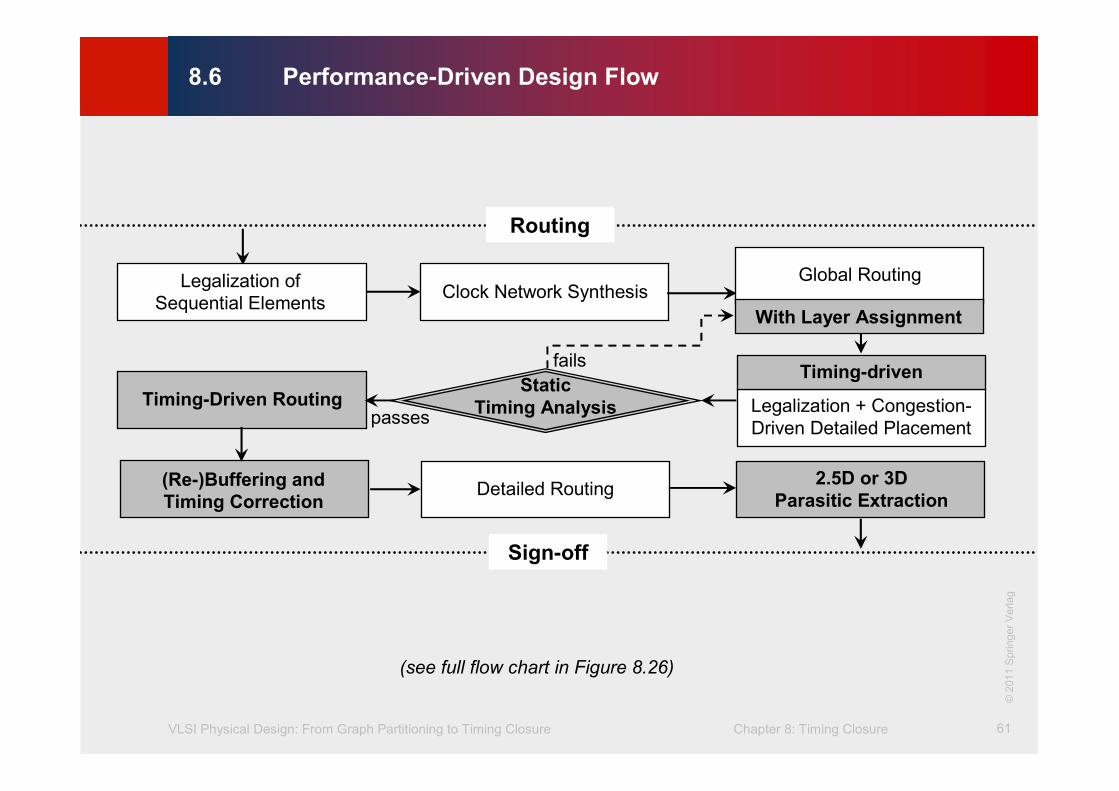
8.6 Performance-Driven Design Flow
Clock Network Synthesis
Timing-driven
Legalization + Congestion-
Driven Detailed Placement
Static
Timing AnalysisTiming-Driven Routing
(Re-)Buffering and
Timing CorrectionDetailed Routing
Global Routing
With Layer Assignment
Routing
Sign-off
fails
passes
Legalization of
Sequential Elements
2.5D or 3D
Parasitic Extraction
(see full flow chart in Figure 8.26)
©201
1 S
pring
er
Verlag

VLSI Physical Design: From Graph Partitioning to Timing Closure Chapter 8: Timing Closure 62
©K
LM
H
Lie
nig
8.6 Performance-Driven Design Flow
Mask Generation
Design Rule Checking
Layout vs. Schematic
Antenna Effects
Electrical Rule Checking
Sign-off
Manufacturability,
Electrical, Reliability
Verification
Static Timing Analysis
ECO Placement and Routing
fails
fails
passes
passes
(see full flow chart in Figure 8.26)
©201
1 S
pring
er
Verlag

VLSI Physical Design: From Graph Partitioning to Timing Closure Chapter 8: Timing Closure 63
©K
LM
H
Lie
nig
Summary of Chapter 8 – Timing Constraints and Timing Analysis
• Circuit delay is measured on signal paths
− From primary inputs to sequential elements; from sequentials to primary outputs
− From sequentials to sequentials
• Components of path delay
− Gate delays: over-estimated by worst-case transition per gate
(to ensure fast Static Timing Analysis)
− Wire delays: depend on wire length and (for nets with >2 pins) topology
• Timing constraints
− Actual arrival times (AATs) at primary inputs and output pins of sequentials
− Required arrival times (RATs) at primary outputs and input pins of sequentials
• Static timing analysis
− Two linear-time traversals compute AATs and RATs for each gate (and net)
− At each timing point: slack = RAT-AAT
− Negative slack = timing violation; critical nets/gates are those with negative slack
• Time budgeting: divides prescribed circuit delay into net delay bounds

VLSI Physical Design: From Graph Partitioning to Timing Closure Chapter 8: Timing Closure 64
©K
LM
H
Lie
nig
Summary of Chapter 8 – Timing-Driven Placement
• Gate/cell locations affect wire lengths, which affect net delays
• Timing-driven placement optimizes gate/cell locations to improve timing
− Interacts with timing analysis to identify critical nets, then biases placement opt.
− Must keep total wirelength low too, otherwise routing will fail
− Timing optimization may increase routing congestion
• Placement by net weighting
− The least invasive technique for timing-driven placement
− Performs tentative placement, then changes net weights based on timing analysis
• Placement by net budgeting
− Allocates delay bounds for each net; translates delay bounds into length bounds
− Performs placement subject to length constraints for individual nets
• Placement based on linear programming
− Placement is cast as a system of equations and inequalities
− Timing analysis and optimization are incorporated using additional inequalities

VLSI Physical Design: From Graph Partitioning to Timing Closure Chapter 8: Timing Closure 65
©K
LM
H
Lie
nig
Summary of Chapter 8 – Timing-Driven Routing
• Timing-driven routing has several aspects
− Individual nets: trading longer wires for shorter source-to-sink paths
− Coupling capacitance and signal integrity: parallel wires act as capacitors
and can slow-down/speed-up signal transitions
− Full-netlist optimization: prioritize the nets that should be optimized first
• Individual net optimization
− One extreme: route each source-to-sink path independently (high wirelength)
− Another extreme: use a Minimum Spanning Tree (low wirenegth, high delay)
− Tunable tradeoff: a hybrid of Prim and Dijkstra algorithms
• Coupling capacitance and signal integrity
− Parallel wires are only worth attention when they transition at the same time
− Identify critical nets, push neighboring wires further away to limit crosstalk
• Full-netlist optimization
− Run trial routing, then run timing analysis to identify critical nets
− Then adjust accordingly, repeat until convergence

VLSI Physical Design: From Graph Partitioning to Timing Closure Chapter 8: Timing Closure 66
©K
LM
H
Lie
nig
Summary of Chapter 8 – Physical Synthesis
• Traditionally, place-and-route have been performed after the netlist is known
• However, fixing gate sizes and net topologies early
does not account for placement-aware timing analysis
− Gate locations and net routes are not available
• Physical synthesis uses information from trial placement to modify the netlist
• Net buffering: splits a net into smaller (approx. equal length) segments
− A long net has high capacitance, the driver may be too weak
• Gate/buffer sizing: increases driver strength & physical size of a gate
− Large gates have higher input pin capacitance, but smaller driver resistance
− Larger gates can drive larger fanouts, longer nets; faster trasitions
− Large gates require more space, larger upstream drivers
• Gate cloning: splits large fanouts
− Cloned gates can be placed separately, unlike with a single larger gate